
 Open Access Article
 This Open Access Article is licensed under a Creative Commons Attribution-Non Commercial 3.0 Unported Licence
Near-UV light emitting diode with on-chip photocatalysts for purification applications†
Young-Chul
Leem
ab,
NoSoung
Myoung
a,
Sang-Hyun
Hong
bc,
Sehee
Jeong
a,
Okkyun
Seo
d,
Seong-Ju
Park
*be,
Sang-Youp
Yim
 *a and
Joon Heon
Kim
*a
*a and
Joon Heon
Kim
*a
aAdvanced Photonics Research Institute, Gwangju Institute of Science and Technology, Gwangju 61005, Korea. E-mail: syim@gist.ac.kr; joonhkim@gist.ac.kr
bSchool of Materials Science and Engineering, Gwangju Institute of Science and Technology, Gwangju 61005, Korea
cGIST Central Research Facilities, Gwangju Institute of Science and Technology, Gwangju 61005, Korea
dCenter for Synchrotron Radiation Research, Japan Synchrotron Radiation Research Institute (JASRI), 1-1-1, Kouto, Sayo, Hyogo 679-5198, Japan
eSchool of Energy Engineering, Korea Institute of Energy Technology, Naju, Jeonnam 58217, Korea. E-mail: sjpark@kentech.ac.kr
First published on 3rd August 2022
Abstract
A new design for light-emitting diodes (LEDs) with on-chip photocatalysts is presented for purification applications. An array of disk-shaped TiO2, with a diameter of several hundred nanometers, combined with SiO2 pedestals was fabricated directly on the surface of an InGaN-based near-ultraviolet (UV) LED using a dry etching process. The high refractive-index contrast at the boundary and the circular shape can effectively confine the near-UV light generated from the LED through multiple internal reflections inside the TiO2 nanodisks. Such a feature results in the enhancement of light absorption by the photocatalytic TiO2. The degradation of the organic dye malachite green was monitored as a model photocatalytic reaction. The proposed structure of LEDs with TiO2/SiO2 nanodisk/pedestal array exhibited a photocatalytic activity that was three times higher than the activity of LEDs with a TiO2 planar layer. The integration of photocatalytic materials with near-UV LEDs in a single system is promising for various purification applications, such as sterilization and disinfection.
Introduction
The demands of the lighting industry for new techniques have led to the development of devices with additional functions beyond high-efficiency lighting sources. Among them, light emitting diodes (LEDs) emitting ultraviolet (UV) light have emerged as one of the most promising technologies because they can be used for a variety of applications, such as polymer curing, insect induction, excitation of fluorescence, phototherapy, medical imaging, sterilization, and disinfection.1–3 Currently, the main application of UV lighting is polymer curing, which mostly requires near-UV light in the wavelength range of 365–400 nm. Near-UV LEDs, in particular InGaN-based LEDs, are a promising alternative for mercury-vapor lamps owing to their advantages, such as high energy efficiency, high sustainability, and environmental friendliness.1Other important applications of UV light are sterilization and disinfection, mostly requiring deep-UV light in the wavelength range of 250–280 nm.4,5 AlGaN-based deep-UV LEDs can emit UV light in this wavelength range, but their use in industrial applications is limited. They present relatively low optical output owing to the strong absorption of UV light in the p-GaN layer resulting in low external quantum efficiency (∼7%). They also exhibit low injection efficiency and vulnerability of internal quantum efficiency to threading dislocations.6–9 Furthermore, the widespread use of deep-UV light is restricted as the exposure of the human body to deep-UV radiation, even for a very short time, can cause severe health issues, such as keratoconjunctivitis or erythema. For example, the threshold energy for symptoms of photokeratitis is only 3.0 mJ cm−2 at a wavelength of 270 nm, whereas near-UV light of much higher energy is required to induce the same effect (4.7 × 10⁴ mJ cm−2 at a wavelength of 380 nm).10 Therefore, the safe use of LEDs is a factor as important as their optical performance for sterilizing/disinfecting applications and should be further examined.
For sterilization/disinfection applications, light can also be used indirectly to excite photocatalytic materials to generate highly reactive radicals, which can decompose toxic chemicals or biomaterials instead of light itself.11,12 Among the various photocatalysts, TiO2 is one of the most widely investigated compounds owing to its novel properties, such as non-toxicity, environmental-friendliness, biocompatibility, low-cost, and corrosion resistance.13–15 Under near-UV illumination, TiO2 can provide bactericidal action, water purification, and disinfection owing to its photocatalytic effect.16–20 Therefore, a combination of TiO2 and near-UV LED with an appropriate geometry for inducing high photocatalytic efficiency is a promising strategy for purification applications.
In general, the absorption of UV photons by TiO2 can induce an electron transition from the valence to the conduction band, accompanied by the creation of holes in the valence band. When excited carriers migrate to the surface of TiO2 photocatalysts they can generate various reactive species, such as hydroxyl (OH) and hydroperoxyl (HO2) radicals. These reactive species can initiate secondary reactions that decompose nearby organic materials leading to sterilization and purification.13,18 Therefore, to enhance photocatalytic activity, light absorption by TiO2, resulting in the generation of electron–hole pairs, should be increased. Meanwhile, the surface-to-volume ratio of the TiO2 structure should be increased to facilitate the diffusion of the generated electrons and holes to the surface before they recombine inside TiO2.14 Therefore, to develop near-UV LEDs with excellent purifying characteristics, it is necessary to construct an optimal photocatalytic LED structure.
To enhance the surface-to-volume ratio of the TiO2 structure on LEDs, an array of zero-dimensional TiO2 nanostructures is preferable to a continuous two-dimensional TiO2 film structure. For example, when the disk diameter is four times the disk thickness, a zero-dimensional TiO2 nanodisk array can provide a surface-to-volume ratio two times higher than that of a two-dimensional TiO2 film (ESI†).
To enhance light absorption by TiO2, the light path length inside TiO2 should be extended by effectively confining the light generated from the active layer of the LED inside the TiO2 materials before its escape. However, previous studies on LEDs with various innovative shapes, such as textured surfaces, photonic crystals, and hierarchical structures, have mostly focused on improving light extraction rather than light trapping.21–23
The high refractive index of TiO2 (n ≈ 3.1) in the near-UV wavelength24 is intrinsically advantageous; high-refractive-index materials surrounded by materials with a low refractive index, such as water (n = 1.3) and air (n = 1), can concentrate the light inside the material by preventing it from escaping for large incidence angle owing to the total internal reflection (TIR) at the boundary. In this regard, the introduction of a disk-shaped TiO2 array onto a near-UV LED can be advantageous; the circular configuration of high-refractive-index materials effectively circulates the obliquely incident light via TIR at its side boundary before its escape, resulting in an extended light path length inside each TiO2 nanodisk.25,26 This increased UV absorption of TiO2 enhances its photocatalytic activity for sterilization and purification.
Herein, we demonstrate the enhanced photocatalytic degradation of organic dyes by a TiO2 nanodisk combined with a flip-chip-structured near-UV LED. The flip-chip structure, in which photons generated in active layers are emitted from the bottom side of the sapphire substrate, is a promising architecture for high-efficiency LEDs owing to its excellent heat dissipation capability, uniform current spreading, and elimination of light propagation hindrance due to bonding pads.27 To fabricate a novel structure combining the TiO2 nanodisk and the flip-chip near-UV LED, a self-assembled silica microsphere monolayer was used as an etching mask to produce the TiO2 nanodisk array from the TiO2 film on the sapphire surface of the near-UV LED.23,28 Moreover, we fabricated a TiO2 nanodisk array with SiO2 pedestals on the sapphire surface of the near-UV LED. Since the refractive index of SiO2 (n = 1.47) is smaller than that of sapphire (n = 1.8),29 the enhanced refractive index contrast at the bottom of the TiO2 nanodisk can further enhance the light-trapping efficiency of the material.
The TiO2 nanodisk array with SiO2 pedestals on the near-UV LED showed approximately three-fold higher activity in the photocatalytic degradation of malachite green (MG) than the flat TiO2 layer on the same LED. The TiO2 nanodisk array without SiO2 pedestals presented 2.2 times higher activity than the flat TiO2 layer. The optical absorption properties of these structures were experimentally studied using UV-visible (UV-vis) absorption spectroscopy and confocal scanning electroluminescence microscopy (CSEM). Theoretical studies were conducted via finite-difference time-domain (FDTD) electromagnetic simulation. All of these confirmed the effectiveness of the use of the TiO2 nanodisk array, especially with SiO2 pedestals, on the near-UV LED structure for photocatalytic applications.
Experimental
Fabrication of near-UV InGaN-based LEDs
Near-UV LEDs, with a dominant emission peak near 370 nm (Fig. S1†), were grown on a c-plane sapphire substrate via metal–organic chemical vapor deposition (MOCVD). After the growth of a 2.5 μm-thick undoped GaN buffer layer, a 2 μm-thick Si-doped n-GaN layer was grown at 1010 °C. Five pairs of InGaN/GaN multiple quantum wells (MQWs) were then grown, followed by a 110 nm-thick p-type GaN layer and a 25 nm-thick p-type AlGaN layer. To fabricate the flip-chip structured LEDs, the p-GaN and MQW layers were partially etched using inductively coupled plasma (ICP) etching until the n-GaN layer was exposed, and Cr/Au-based n-pad electrodes were deposited via electron beam evaporation. LEDs of 300 μm × 300 μm size were fabricated by depositing an Ag-based p-pad electrode on the p-GaN layer via electron beam evaporation (Fig. 1, inset). | ||
| Fig. 1 Schematic of the fabrication steps of the TiO2/SiO2 nanodisk/pedestal array on the near-UV LED: Dip-coating for self-assembling the silica spheres (1 μm in diameter) on the TiO2 layer; dry etching of the TiO2/SiO2 layer using the close-packed silica sphere monolayer as an etching mask; removal of the residual silica spheres using an adhesive tape; metallization to form p- and n-electrode metals. Inset illustrates the cross-sectional view of the final structure with the TiO2/SiO2 nanodisk/pedestal array on the near-UV LED. | ||
Fabrication of TiO2/SiO2 nanodisk structures
Fig. 1 presents the manufacturing process of the disk-shaped TiO2 photocatalytic layer with SiO2 pedestals on the surface of a sapphire substrate, which is the opposite side of the GaN-based epitaxial layers of the flip-chip near-UV LED. First, a 200 nm-thick SiO2 layer was grown on a sapphire substrate via plasma-enhanced chemical vapor deposition, and then a 200 nm-thick TiO2 layer was deposited through electron beam evaporation. The amorphous TiO2 thin film was annealed at 450 °C for 3 h in atmospheric pressure to convert TiO2 to the anatase phase, which is known to provide the highest photocatalytic activity among the TiO2 crystal structures. The surface of the TiO2 thin film was pretreated with oxygen plasma for 5 min to reduce its surface energy and facilitate the dip-coating process of the two-dimensional (2D) colloidal layer. A hexagonal close-packed (HCP) 2D colloidal crystal composed of 1 μm diameter silica spheres was deposited on the surface via dip-coating using 15 wt% of a silica colloidal suspension in ethanol.23 Next, ICP etching, using the HCP silica monolayer as an etching mask, was conducted to form a hexagonal array of the disk-shaped TiO2/SiO2 layer with a diameter of 750 nm. After ICP etching, the residual silica spheres on the TiO2/SiO2 nanodisk array were gently removed by attaching and peeling the adhesive tape.Optical measurements using UV-vis absorption spectroscopy and CSEM
The UV-vis absorption spectra of the TiO2 nanodisk and the TiO2/SiO2 nanodisk/pedestal arrays fabricated on the sapphire substrate were measured in the transmission geometry using a PerkinElmer Lambda 900 UV/vis/NIR spectrophotometer. CSEM measurements were performed using a modified commercial confocal scanning microscope (WITec GmbH). The electroluminescence (EL) light was collected from the samples using a microscope objective (×100, NA 0.9) and delivered to the detector (photomultiplier tube, PMT) via a multimode optical fiber (φcore = 50 μm) for EL mapping. During the experiments, an injection current of 20 mA from a Keithley 2450 current source was applied to the LED. The spatial EL distribution for the 5 × 5 μm2 region was obtained in 10 nm steps using a piezoelectric (PZT) nano-positioning stage.Three-dimensional FDTD simulation
FDTD simulation was performed using a commercially available software (Lumerical FDTD Solutions) to investigate light propagation through the hierarchical surface structures of the LEDs. A point dipole source polarized along the y axis was located in the center of the MQWs to simulate light generated from the LED as transverse electric (TE) polarization was predominantly observed in InGaN/GaN MQW LEDs.30–32 The point dipole source was assumed to emit monochromatic light with a wavelength of 370 nm. The simplified LED structure for the FDTD simulation was composed of a 100 nm-thick Ag mirror, 110 nm-thick p-GaN layer, 100 nm-thick InGaN/GaN MQW layer, 2 μm-thick n-GaN layer, 2.5 μm-thick undoped GaN layer, and 750 nm-diameter TiO2/SiO2 nanodisk. The model structure of the LED was surrounded by a perfectly matched layer (PML).33Evaluation of the photocatalytic purifying activity
The photocatalytic purifying activity of the fabricated near-UV LEDs with TiO2 nanodisks was evaluated by investigating the photocatalytic degradation of MG in water at room temperature.34 A cylindrical cell with an inner diameter of 8 mm was built on top of the photocatalytic structure of the LED and was filled with a 100 μL aqueous MG solution with a concentration of 0.1 g L−1 (Fig. S2†). After waiting for 1 h in the dark to establish an adsorption/desorption equilibrium of MG on the photocatalytic layer, the near-UV LED was turned-on at an injection current of 20 mA to illuminate the photocatalytic layer on the LED surface by the near-UV LED light at a peak wavelength of 370 nm. During the photocatalytic degradation of MG in the aqueous solution, the reaction cell was covered with a glass to prevent the evaporation of the solution. The degradation rate of the MG solution was determined by the change in its concentration. To calculate the MG concentration, the absorbance of the solution was monitored in 30 min intervals using an optical microscope equipped with a collimated external LED light source with a nominal wavelength of 617 nm, which is close to the absorption peak of MG (Fig. S3†).Results and discussion
Fig. 2a and b present the scanning electron microscope (SEM) images and a photograph (inset) of the homogeneous formation of the HCP 2D colloidal crystal of silica microspheres covering a large area on the TiO2/SiO2 layer grown on a sapphire substrate with a diameter of 2 inches. The photograph of the silica sphere monolayer shows green iridescence owing to the constructive interference of visible light by the ordered colloidal crystal, which is similar to the photonic crystal. The top-view SEM images of the HCP 2D colloidal crystal clearly show the long-range ordering of silica spheres. The inset of Fig. 2b represents a cross-sectional SEM image of the residual silica spheres together with the etched TiO2/SiO2 layer after the ICP etching.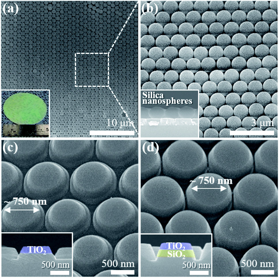 | ||
| Fig. 2 (a) Two-dimensional colloidal crystal on a TiO2/SiO2 layer grown on a 2 inch-diameter sapphire substrate. (b) Top-view SEM image of the 2D hexagonal crystal of silica spheres with a diameter of 1 μm before ICP etching. Inset is the cross-sectional SEM image of the residual silica spheres on the TiO2/SiO2 nanodisk/pedestal array after ICP etching. SEM images with a 45°-inclined angle view of (c) pristine TiO2 nanodisk array and (d) TiO2/SiO2 nanodisk/pedestal array. Insets are the corresponding cross-sectional SEM images of nanodisks. | ||
As the ICP etching progressed, the pristine TiO2 nanodisk array on the sapphire substrate formed below the silica sphere layers with a concomitant reduction in the size of each silica sphere (Fig. 2). By changing the ICP etching time, the diameter of nanodisks can be controlled (Fig. S4†). Fig. 2c and d show the bird's-eye view SEM images of the TiO2 nanodisks and the TiO2 nanodisks with SiO2 pedestals with a diameter of 750 nm, respectively. These nanodisks were used for following experiments.
The current–voltage (I–V) characteristics of the near-UV LEDs with different structures (planar TiO2 film, TiO2 nanodisk array, and TiO2/SiO2 nanodisk/pedestal array) show similar forward voltages of 3.46–3.48 V, as shown in Fig. S5.† The identical I–V characteristic curves of the LEDs with the four different surface structures indicate that the fabrication process of TiO2 nanodisks, including ICP etching and annealing to convert TiO2 from the amorphous to the anatase phase, does not affect the electrical properties of the LEDs.
To investigate the crystal properties of the TiO2 nanodisks, we performed X-ray diffraction (XRD) measurements using the 5D GIST beamline of the Pohang Light Source (PLS) in Korea. The X-ray energy was set at 10 keV (1.24 Å) using a double-bounced Si (111) monochromator (ESI, Fig. S6†). The XRD profiles of the TiO2 films with and without the annealing process at 450 °C for the substrate's normal direction are shown in Fig. 3. The XRD profiles of these two structures commonly show a predominant sapphire (0006) diffraction peak at 33.27°. The XRD profile of the annealed TiO2 film clearly showed peaks corresponding to the anatase phase of the TiO2 crystal planes of (101), (004), (200), (105), (211), (213), (220), and (215) with lattice constants of a = b = 3.78 Å and c = 9.49 Å (JCPDS PDF #00-064-0863). The TiO2 film without annealing showed no significant peaks related to the TiO2 crystal phase.
 | ||
| Fig. 3 XRD patterns of the TiO2 film on the sapphire substrate with and without annealing at 450 °C for 3 h. | ||
To investigate the optical properties of the TiO2 and TiO2/SiO2 nanodisk structures, their absorption spectra were compared with those of the film structures using a UV-vis absorption spectrometer (Fig. 4). As the wavelength decreased, the absorption rapidly increased from approximately 390 nm for both the planar TiO2 and TiO2/SiO2 films. This value corresponds to the band gap energy of 3.2 eV, which is a characteristic of TiO2.14 However, the absorbance in the wavelength range of 365–400 nm corresponding to the near-UV light from the InGaN LED is much weaker compared to that at shorter wavelengths. Therefore, to enhance the photocatalytic efficiency of the InGaN LED, it is necessary to increase the absorption by extending the light path length through alterations in the structure of the TiO2 layer.
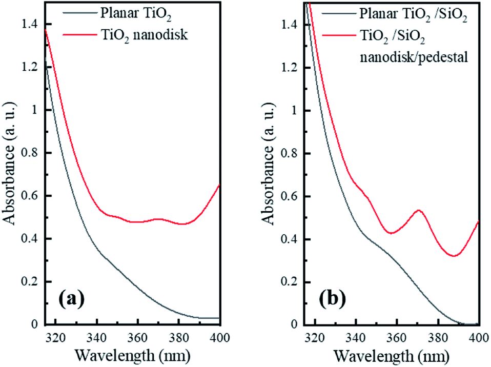 | ||
| Fig. 4 UV-vis absorption spectra of (a) pristine TiO2 nanodisks and (b) TiO2 nanodisks on SiO2 pedestals compared to their planar films. | ||
As shown in Fig. 4, the TiO2 and TiO2/SiO2 nanodisk array structures presented much higher absorbance values than the planar TiO2 and TiO2/SiO2 films in the wavelength range of the near-UV light (365–400 nm) from the InGaN LED. The increased absorbance of the nanodisk array can be attributed to the increased scattering as well as the extended path length of the light inside the TiO2 nanodisks through TIR. In contrast to the planar layer, the nanodisk array can significantly scatter incident light, and part of the obliquely scattered light can be re-absorbed by the nearby nanodisks. Once the light is injected into the TiO2 nanodisk, the high refractive index contrast between TiO2 (n = 3.1 for 370 nm)24 and air (n = 1) at the TiO2/air boundary can be advantageous in reducing the light escaping from the side edge as well as the top plane of the nanodisk via TIR. In addition, the circular shape of the TiO2 nanodisk is beneficial for circulating light inside the structure through multiple internal reflections at its circumference.
Fig. 5 shows the photocatalytic degradation of MG as a function of the LED operating time for various TiO2-based surface configurations, such as the planar TiO2 film, TiO2 nanodisk array, and TiO2/SiO2 nanodisk/pedestal array. The time-dependent change of the MG concentration shows a typical single-exponential decay curve whose rate is different for various TiO2 structures. To compare the degradation rate of each structure, the ln-linear plot of the MG concentration versus time was fitted to the following equation:
ln![[thin space (1/6-em)]](https://www.rsc.org/images/entities/char_2009.gif) C − lnC0 = −kt C − lnC0 = −kt | (1) |
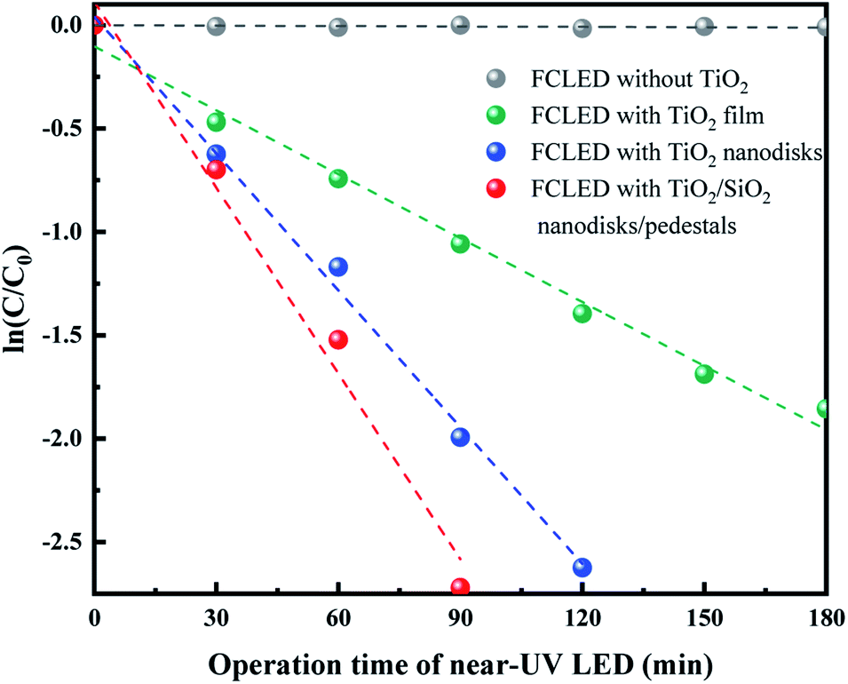 | ||
| Fig. 5 Photocatalytic degradation of MG as a function of the operation time of LEDs for the planar TiO2 film, TiO2 nanodisk array, and TiO2/SiO2 nanodisk/pedestal array. Each dashed line presents the linear fitting for the measured data. | ||
In the absence of TiO2, the MG concentration did not change, which confirms that the near-UV light at approximately 370 nm cannot directly degrade MG molecules under the experimental conditions. When the near-UV light illuminated TiO2, MG was drastically degraded, with the degradation rate being different for different TiO2 structures. The measured degradation rates of the LEDs with the planar TiO2 film, TiO2 nanodisk array, and TiO2/SiO2 nanodisk/pedestal array were 0.010, 0.022, and 0.030 min−1, respectively. The TiO2/SiO2 nanodisk/pedestal array exhibited three and 1.4 times higher photocatalytic activity than the planar TiO2 layer and the TiO2 nanodisk array without SiO2 pedestals, respectively. The higher photocatalytic activity of the TiO2/SiO2 nanodisk/pedestal array compared to that of other structures should be related to the more confinement and absorption of near-UV light inside TiO2.
The optical properties of the nanodisk structures were examined by performing three-dimensional FDTD simulations at 370 nm (the peak wavelength of our InGaN-based near-UV LED), for the TiO2 and TiO2/SiO2 nanodisks (Fig. 6). Fig. 6a–d show the electric field distribution in the TiO2 and TiO2/SiO2 nanodisk structures when light from the LED is obliquely incident on the TiO2 nanodisks. The very high intensity inside the TiO2 nanodisk compared to that outside it clearly shows the effective confinement of light inside the TiO2 nanodisk. In addition, the formation of strong modes around the circumference is clear in the TiO2/SiO2 nanodisk/pedestal structure (Fig. 6c), while the modes are slightly weaker in the TiO2 nanodisk without the SiO2 pedestal structure (Fig. 6a).
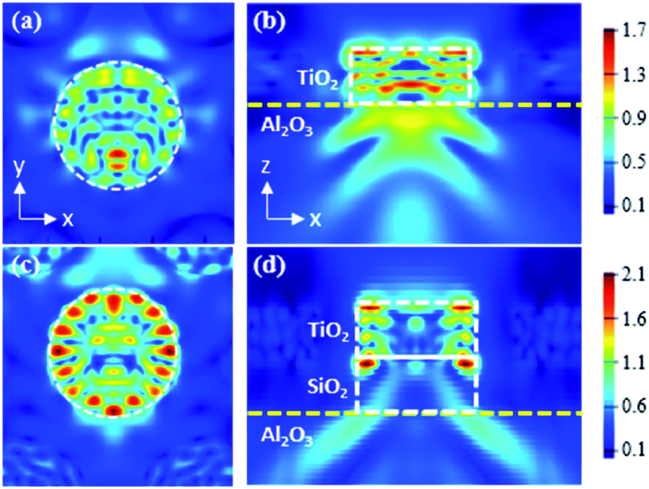 | ||
| Fig. 6 Simulated electric field distribution in the x–y plane and the cross-sectional (x–z) plane of (a and b) pristine TiO2 nanodisk and (c and d) TiO2/SiO2 nanodisk/pedestal. Dashed lines indicate the position of the nanodisk. | ||
The modes along the circumference indicate that the light inside the TiO2 nanodisk can be repetitively reflected at its circular boundary without significant escape. During multiple internal reflections, light can be greatly absorbed by TiO2 to enhance a photocatalytic effect. The escape of light from the top plane of the TiO2 nanodisk was not significant, mostly because of the high refractive index contrast at the TiO2/air boundary (3.1/1.0). For this refractive index contrast, all the incident light from the TiO2 side at an incident angle larger than the TIR critical angle of 19° should be totally reflected.
The TIR effect on the confinement of light worked in a similar way for the bottom plane of the TiO2 nanodisk. However, the confinement effect of light inside TiO2 at the bottom plane should be weaker than that of the top plane owing to the smaller refractive index contrast at the TiO2/sapphire boundary (3.1/1.8), for which the TIR critical angle is 35°. In this regard, the use of a SiO2 layer (n = 1.47) between TiO2 and sapphire, whose refractive index is smaller than that of sapphire (n = 1.8), can further reduce the lower-direction escape of light from the TiO2 nanodisk at the bottom side. Such a layer can increase the refractive index contrast at the bottom plane of the TiO2 nanodisk (TIR angle = 28°), although the coupling efficiency from the LED to the TiO2 nanodisk can be concomitantly decreased.
Furthermore, the double height of the TiO2/SiO2 nanodisk/pedestal structure compared to that of the TiO2 nanodisk can be advantageous for the re-absorption of the light escaping from the side edge of the nanodisk by the neighboring nanodisks. All these factors contribute to the enhanced photocatalytic activity of the TiO2/SiO2 nanodisk/pedestal structure.
The intensity of the light escaping from the TiO2 nanodisk and TiO2/SiO2 nanodisk/pedestal arrays was experimentally measured via CSEM (Fig. 7) to compare the light confinement effects. As expected, the intensity of the light that escaped from the circular edge of the TiO2 nanodisk was much lower than that escaping from the central part of the top plane of the nanodisk. During multiple reflections of light between the bottom and top disk planes of the TiO2 nanodisk, the vertically incident light on its surface, mostly at the central part of the plane, can be partially transmitted. This possibly occurs owing to the low incident angle, despite the high refractive index contrast between TiO2 and air. However, the reflectance at the TiO2/air boundary is approximately 26% even under normal incidence conditions, which implies that a substantial amount of light can be reflected back to the inside of the structure, even for a very small incident angle. For larger incident angles, the reflectance can be significantly increased. A comparison of Fig. 7a and b shows that the intensity of the light escaping from the TiO2/SiO2 nanodisk/pedestal array was weaker than that of the TiO2 nanodisk array for the same injection current. This finding indicates that the TiO2/SiO2 nanodisk/pedestal array is more effective in confining the LED light in their nanostructures than the TiO2 nanodisk array, as expected.
 | ||
| Fig. 7 Experimental CSEM images of (a) TiO2 nanodisk array and (b) TiO2/SiO2 nanodisk/pedestal array on the near-UV LED at an injection current of 20 mA. Circular dashed lines indicate the position of nanodisks. | ||
Conclusions
In summary, we demonstrated a new type of light source for photocatalytic purification applications by directly fabricating anatase-phase TiO2 nanostructures on the surface of an InGaN-based near-UV LED. A TiO2 nanodisk array with SiO2 pedestals has been proposed as an effective structure for maximizing the light-trapping efficiency and surface-to-volume ratio of the TiO2 layer. The high refractive index contrast and the circular shape of the boundary, which were advantageous for multiple reflections, resulted in strong optical confinement. This increased the effective absorption of the near-UV light by TiO2, resulting in a high photocatalytic activity. The photocatalytic activity of this structure in degrading MG was approximately three times higher than that of the planar TiO2 film when combined with the near-UV LED. In conclusion, it is expected that this study can provide a guideline for the design of integrated photocatalytic materials and LEDs in a single system for various purification applications, such as sterilization and disinfection.Author contributions
Young-Chul Leem: conceptualization, methodology, investigation, formal analysis, writing – original draft. NoSoung Myoung: investigation. Sang-Hyun Hong: software. Sehee Jeong: investigation. Okkyun Seo: investigation. Seong-Ju Park: conceptualization, resources, writing – review & editing. Sang-Youp Yim: conceptualization, formal analysis, writing – review & editing. Joon Heon Kim: conceptualization, methodology, supervision, writing – review & editing.Conflicts of interest
There are no conflicts to declare.Acknowledgements
This research was supported by the National Research Foundation of Korea (NRF) grant funded by the MSIT of Korea government (NRF-2021R1A2C1008787, NRF-2020R1F1A1076964) and by GIST Research Institute (GRI) grant funded by the GIST in 2022.References
- Y. Muramoto, M. Kimura and S. Nouda, Semicond. Sci. Technol., 2014, 29, 084004 CrossRef CAS.
- K. Song, M. Mohseni and F. Taghipour, Water Res., 2016, 94, 341–349 CrossRef CAS PubMed.
- N. G. Yeh, C. H. Wu and T. C. Cheng, Renewable Sustainable Energy Rev., 2010, 14, 2161–2166 CrossRef CAS.
- T. Bintsis, E. Litopoulou-Tzanetaki and R. K. Robinson, J. Sci. Food Agric., 2000, 80, 637–645 CrossRef CAS PubMed.
- J. Chen, S. Loeb and J. H. Kim, Environ. Sci.: Water Res. Technol., 2017, 3, 188–202 RSC.
- D. Y. Kim, J. H. Park, J. W. Lee, S. Hwang, S. J. Oh, J. Kim, C. Sone, E. F. Schubert and J. K. Kim, Light: Sci. Appl., 2015, 4, e263 CrossRef CAS.
- H. Hirayama, N. Maeda, S. Fujikawa, S. Toyoda and N. Kamata, Jpn. J. Appl. Phys., 2014, 53, 100209 CrossRef.
- K. Ban, J. I. Yamamoto, K. Takeda, K. Ide, M. Iwaya, T. Takeuchi, S. Kamiyama, I. Akasaki and H. Amano, Appl. Phys. Express, 2011, 4, 052101 CrossRef.
- Y. Kuo, C. Y. Su, C. Hsieh, W. Y. Chang, C. A. Huang, Y. W. Kiang and C. C. Yang, Opt. Lett., 2015, 40, 4229–4232 CrossRef CAS PubMed.
- Ultraviolet Radiation Guide, Navy Environmental Health Center, Norfolk, Virginia, 1992 Search PubMed.
- J. M. Herrmann, Catal. Today, 1999, 53, 115–129 CrossRef CAS.
- M. R. Hoffmann, S. T. Martin, W. Choi and D. W. Bahnemann, Chem. Rev., 1995, 95, 69–96 CrossRef CAS.
- J. Schneider, M. Matsuoka, M. Takeuchi, J. Zhang, Y. Horiuchi, M. Anpo and D. W. Bahnemann, Chem. Rev., 2014, 114, 9919–9986 CrossRef CAS PubMed.
- K. Nakata and A. Fujishima, J. Photochem. Photobiol., C, 2012, 13, 169–189 CrossRef CAS.
- K. P. Gopinath, N. V. Madhav, A. Krishnan, R. Malolan and G. Rangarajan, J. Environ. Manage., 2020, 270, 110906 CrossRef CAS PubMed.
- D. Gumy, C. Morais, P. Bowen, C. Pulgarin, S. Giraldo, R. Hajdu and J. Kiwi, Appl. Catal., B, 2006, 63, 76–84 CrossRef CAS.
- M. Cho, H. Chung, W. Choi and J. Yoon, Water Res., 2004, 38, 1069–1077 CrossRef CAS PubMed.
- A. Fujishima, T. N. Rao and D. A. Tryk, J. Photochem. Photobiol., C, 2000, 1, 1–21 CrossRef CAS.
- D. Bertagna Silva, G. Buttiglieri and S. Babić, Environ. Sci. Pollut. Res., 2021, 28, 103–120 CrossRef CAS PubMed.
- T. S. Natarajan, M. Thomas, K. Natarajan, H. C. Bajaj and R. J. Tayade, Chem. Eng. J., 2011, 169, 126–134 CrossRef CAS.
- J. J. Wierer Jr, A. David and M. M. Megens, Nat. Photonics, 2009, 3, 163–169 CrossRef.
- W. C. H. Choy, W. K. Chan and Y. Yuan, Adv. Mater., 2014, 26, 5368–5399 CrossRef CAS PubMed.
- Y. C. Leem, J. S. Park, J. H. Kim, N. Myoung, S. Y. Yim, S. Jeong, W. Lim, S. T. Kim and S. J. Park, Small, 2016, 12, 161–168 CrossRef CAS PubMed.
- A. Bendavid and P. J. Martin, J. Aust. Ceram. Soc., 2014, 50, 86–101 CAS.
- S. Yang, Y. Wang and H. D. Sun, Adv. Opt. Mater., 2015, 3, 1136–1162 CrossRef CAS.
- J. Park, S. K. Ozdemir, F. Monifi, T. Chadha, S. H. Huang, P. Biswas and L. Yang, Adv. Opt. Mater., 2014, 2, 711–717 CrossRef CAS.
- J. J. Wierer, D. A. Steigerwald, M. R. Krames, J. J. O'Shea, M. J. Ludowise, G. Christenson, Y. C. Shen, C. Lowery, P. S. Martin, S. Subramanya, W. Götz, N. F. Gardner, R. S. Kern and S. A. Stockman, Appl. Phys. Lett., 2001, 78, 3379–3381 CrossRef CAS.
- L. Han, T. A. Piedimonte and H. Zhao, Opt. Mater. Express, 2013, 3, 1093–1100 CrossRef.
- M. J. Dodge, Handbook of Laser Science and Technology, Volume IV, Optical Materials: Part 2, CRC Press, Boca Raton, 1986 Search PubMed.
- K. B. Nam, J. Li, M. L. Nakarmi, J. Y. Lin and H. X. Jiang, Appl. Phys. Lett., 2004, 84, 5264–5266 CrossRef CAS.
- A. David, C. Meier, R. Sharma, F. S. Diana, S. P. Denbaars, E. Hu, S. Nakamura, C. Weisbuch and H. Benisty, Appl. Phys. Lett., 2005, 87, 101107 CrossRef.
- J. Shakya, K. Knabe, K. H. Kim, J. Li, J. Y. Lin and H. X. Jiang, Appl. Phys. Lett., 2005, 86, 091107 CrossRef.
- J. P. Berenger, J. Comput. Phys., 1994, 114, 185–200 CrossRef.
- K. Natarajan, T. S. Natarajan, H. C. Bajaj and R. J. Tayade, Chem. Eng. J., 2011, 178, 40–49 CrossRef CAS.
Footnote |
| † Electronic supplementary information (ESI) available. See https://doi.org/10.1039/d2na00305h |
| This journal is © The Royal Society of Chemistry 2022 |