
 Open Access Article
 This Open Access Article is licensed under a Creative Commons Attribution-Non Commercial 3.0 Unported Licence
Monolayer NaW2O2Br6: a gate tunable near-infrared hyperbolic plasmonic surface†
Enhui
Huang‡
a,
Hui
Xiang‡
 b,
Han
Jiao
a,
Xia
Zhou
a,
Jinli
Du
a,
Wenying
Zhong
*a and
Bo
Xu
*a
b,
Han
Jiao
a,
Xia
Zhou
a,
Jinli
Du
a,
Wenying
Zhong
*a and
Bo
Xu
*a
aSchool of Science and Key Laboratory of Biomedical Functional Materials, China Pharmaceutical University, Nanjing 211198, P. R. China. E-mail: wyzhong@cpu.edu.cn; xubo@cpu.edu.cn
bSchool of Mathematics and Physics, Hubei Polytechnic University, Huangshi, 435003, P. R. China
First published on 5th July 2022
Abstract
Electrically tunable hyperbolic polaritons in two dimensional (2D) materials can offer unexplored opportunities in integrating photonics and nano-optoelectronics into a single chip. Here, we suggest that monolayer NaW2O2Br6 can host electrically tunable hyperbolic plasmon polaritons for infrared light via first-principles calculations. 2D monolayer NaW2O2Br6 exhibits an extremely anisotropic metallic property: conducting for one direction but almost insulating for the other direction, which could be considered as a 2D analogue of metal/dielectric multilayers, a typical structure for hyperbolic metamaterials. More interestingly, we also demonstrate that the hyperbolic properties in the near-infrared range, including the hyperbolic windows, figure of merit, and propagation directions of plasmon beams, can be effectively modulated by carrier doping at the order of 1013 cm−2, which even can be accessed by solid-gated field effect transistors. Thus, it is anticipated that monolayer NaW2O2Br6 has a great potential in constructing field programmable polariton nanodevices for emerging and diverse photonic applications.
Introduction
Because of the extraordinary ability to control light down to the atomic length-scale, two dimensional (2D) materials hosting hyperbolic polaritons have emerged as one of the most attractive research interests in the past few years.1–3 In particular, several 2D materials, such as BN,4–6 MoO3,7–10 and V2O5,11 have been demonstrated to possess hyperbolic phonon polaritons (PhPs) with excellent properties, such as long lifetimes, low loss and strong field confinement, and offer as yet unexplored opportunities for photonic and optoelectronic devices. However, hyperbolic PhPs, the hybrid excitation of light and lattice vibration, usually are hard to control and tune by electric fields, indicating that it still remains a challenge to integrate hyperbolic PhPs into nanophotonic and optoelectronic circuits.Compared to PhPs, plasmon polaritons (PPs)12,13 show great potential in gate control devices, because of the dependence of plasma frequency (ωp) on the carrier density: ωp2 = ne2/ε0m*, in which n is the carrier density, and m* is the effective mass of the carrier. Graphene,14 a special 2D metal with no intrinsic carrier, is a perfect carrier tunable plasmonic material. Periodic graphene strips15,16 are suggested to exhibit tunable hyperbolic PPs in the THz region due to the adjustable Fermi levels upon the gate voltages. WTe2, an anisotropic semimetal, was demonstrated to be a natural hyperbolic plasmonic surface in the far-IR range.17,18 2D in-plane anisotropic semiconductors, such as black phosphorus19,20 and TiS3,21 are theoretically proposed to exhibit natural tunable hyperbolic plasmonic behaviors for near infrared (NIR) light by carrier doping. However, these proposed hyperbolic PPs in the NIR range can be realized only when the carrier densities reach 1014 cm−2. Recently, anisotropic 2D metals, such as boron,22,23 MoOCl2,24 and CuB3,25 are indicated as natural hyperbolic surfaces due to their anisotropic metallic properties. Attributed to their high intrinsic carrier densities, up to 1015 cm−2, outstanding hyperbolic PPs, such as low losses and wide hyperbolic windows, can even work in the visible light range. But just because of the high intrinsic carrier concentrations, these hyperbolic PPs in 2D metals usually are not sensitive to the gate voltages. To modulate these plasmonic properties by carriers, the tunable carrier density should be up to 1014 cm−2 at least. As we see, despite the potential of these hyperbolic PPs for on-chip photonic devices, candidates with electrically tunable hyperbolic PPs are still rare, especially in the short wave range, attributed to the high required carrier density, up to 1014 cm−2. Thus, from an integration perspective, it is urgent to explore electrically tunable hyperbolic PPs.
Herein, based on first-principles calculations, we found that monolayer NaW2O2Br6 is a potential candidate for electrically tunable hyperbolic PPs for NIR light. Monolayer NaW2O2Br6 could be regarded as a 2D analogue of metal/dielectric multilayers owing to its extremely anisotropic metallic property, conducting for one direction but almost insulating for the other direction. It results in monolayer NaW2O2Br6 with natural hyperbolic PPs for infrared light. Due to low intrinsic carrier concentration, only about 2.5 × 1014 cm−2, the hyperbolic PPs in the NIR range are suggested to be tunable even by solid-gated field effect transistors (FETs), which shows great advantages in integrated optical devices.
Results
Anisotropic crystal structure of monolayer NaW2O2Br6
Orthorhombic NaW2O2Br6 was experimentally reported as a layered material with mixed valence tungsten.26 The optimized crystal structure of monolayer NaW2O2Br6 is displayed in Fig. 1a with a large unit cell size of about 40 Å2 (a = 3.82 Å, and b = 10.54 Å). Detailed structure information is supplied in the ESI (Table S1†). As we see, monolayer NaW2O2Br6 exhibits an extremely anisotropic crystal structure. The W atoms are sixfold coordinated by two O atoms and four Br atoms to form [WO2Br4] octahedra, which are condensed to pairs via a common Br2 edge and condensed via the oxygen ligands to form 1D [W2O2Br6]− anionic chains along the x direction. These 1D chains are interconnected by the Na+ cations to form a 2D structure. By counting the electron number, we found that there is one electron per unit cell, resulting in a carrier concentration of 2.5 × 1014 cm−2, about one order less than those in traditional 2D metals, such as boron22,23 and TaS2.27 By the carrier density mapping in Fig. 1b, we see that a one-dimensional electron gas (1DEG) is confined primarily in the [W2O2Br6] chains and separated by Na+ cations. As can be seen from the line plot in Fig. 1c, the width of the 1DEG is about 0.5–0.6 nm. The inhomogeneous carrier distribution in monolayer NaW2O2Br6 indicates an extremely anisotropic metallic behavior: conducting along the x direction, but almost insulating along the y direction. It looks like a natural 2D metal/dielectric multilayer (Fig. 1d), which is a typical structure to design hyperbolic metamaterials.28 Thus, monolayer NaW2O2Br6 may be a natural candidate to host hyperbolic PPs. Moreover, the periodicity of a metal/dielectric multilayer in monolayer NaW2O2Br6 is only about 1 nm, about one order less than those in traditional metal/dielectric multilayered hyperbolic metamaterials.28 Such hyperbolic PPs in natural materials have significant advantages for potential applications. Apparently, they not only can avoid complex fabrication processes for hyperbolic devices. Compared to metamaterials, natural materials have much larger Brillouin zones, which can overcome the limitation of wave vectors attributed to the size of the Brillouin zone.10,28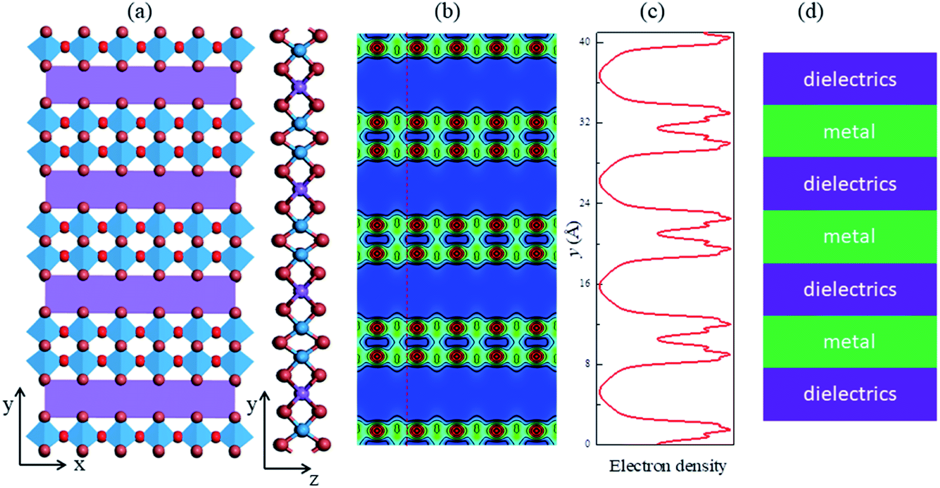 | ||
| Fig. 1 Anisotropic structure of monolayer NaW2O2Br6. (a) Top and side views of crystal structure of monolayer NaW2O2Br6. Blue, brown, red and purple balls represent W, Br, O, and Na atoms, respectively. W atoms are coordinated by two O atoms and four Br atoms to form WO2Br4 octahedra. (b) Real space electron density distribution of monolayer NaW2O2Br6. (c) The line plot electron density distribution of the red dashed line in (b). (d) Such electron distribution can be regarded as a natural metal/dielectric multilayer, a typical hyperbolic metamaterial system. | ||
Anisotropic electronic and optical properties of monolayer NaW2O2Br6
Before investigating the hyperbolic properties in monolayer NaW2O2Br6, we first performed density functional theory (DFT) calculations (see Methods) for its electronic properties. Fig. 2a displays the calculated orbital projected band structure for monolayer NaW2O2Br6, obtained from HSE hybrid density functional calculations. dxz and dxy orbitals of W dominate the low energy states around the Fermi level, with little hybridization with Br-4p orbitals. Based on the band structure, monolayer NaW2O2Br6 is an extremely anisotropic metal. Usually, the anisotropy of a metal is expressed by different dispersions for different directions. For monolayer NaW2O2Br6, it is quite different. As shown in Fig. 2a, for the x direction (Γ to X and Y to S paths), two well dispersed bands, contributed by dxz and dxy orbitals, respectively, cross the Fermi level. But for the y direction (Γ to Y and X to S paths), no band crosses the Fermi level, and it looks like a semiconductor with rather flat conduction and valence bands. Both the highest occupied band and the lowest unoccupied band are mainly composed of the dxz orbital. These extremely anisotropic electronic properties are consistent with our previous analysis by the charge density that monolayer NaW2O2Br6 is like a 2D metal/dielectric multilayer.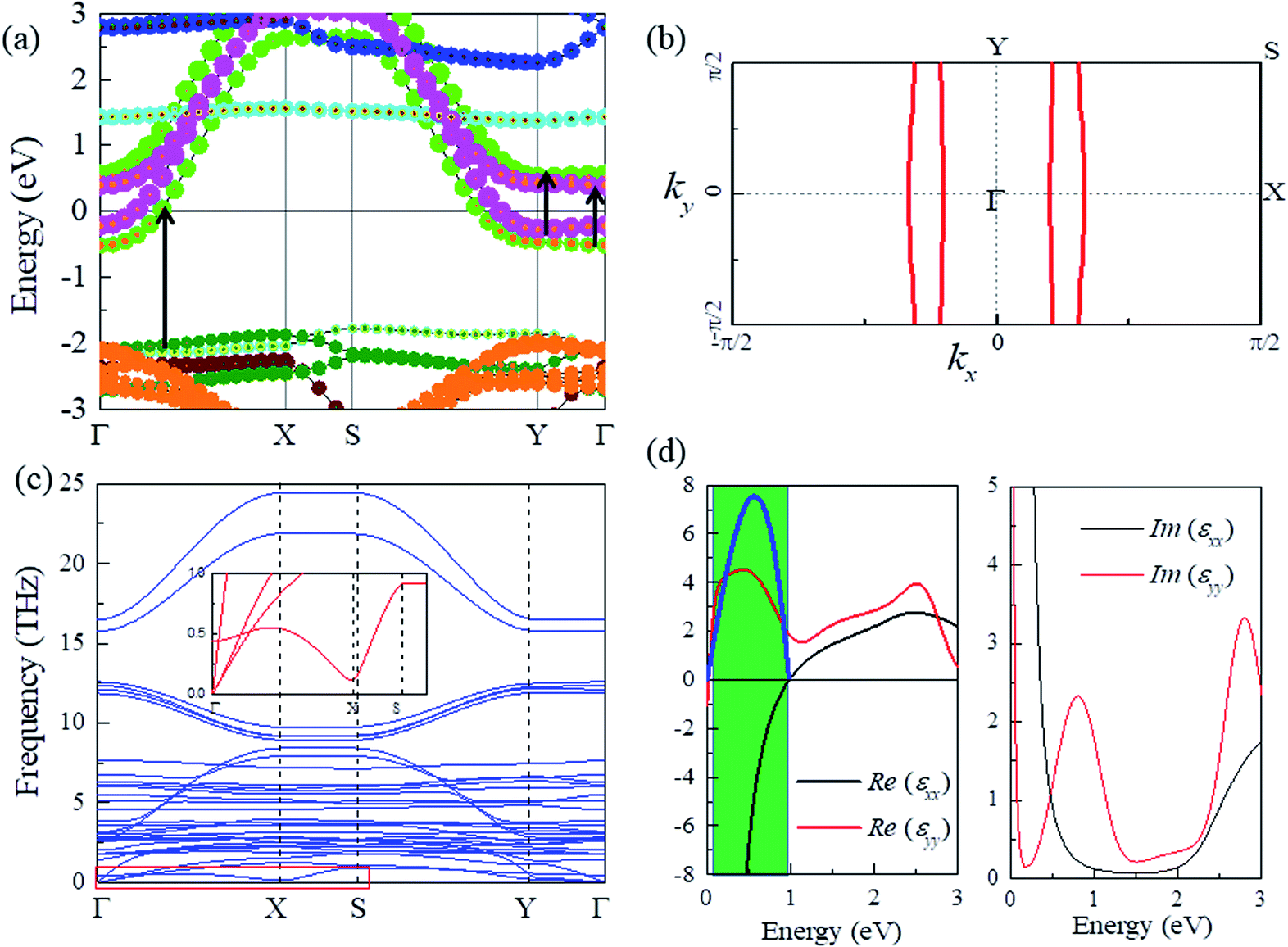 | ||
| Fig. 2 Extremely anisotropic electronic properties and hyperbolic PPs. (a) Orbital projected band structure for monolayer NaW2O2Br6. Green, blue, cyan, and purple dots represent dxy, dyz, dz2 and dxz orbitals of W atoms, respectively. Orange, wine and olive dots (b) represent px, py and pz orbitals of Br atoms, respectively. (c) The phonon dispersion of monolayer NaW2O2Br6. The inset (red line) is the magnification of phonon dispersion around the X point. (d) The real and imaginary parts of dielectric functions along x and y directions, respectively. Between 0.03 and 0.98 eV, it is hyperbolic for Re(εyy) is positive, whereas Re(εxx) is negative. The blue line in (d) is the FoM in the hyperbolic range. | ||
To further demonstrate this extremely anisotropic metallic property, we plot the Fermi surface (FS) for monolayer NaW2O2Br6 in Fig. 2b. Notably, it displays an extremely anisotropic character: there are two sets of almost parallel lines along the ky direction. As a result, no band crosses the Fermi level along the y direction. Materials with such extremely anisotropic FSs usually are unstable at low temperature, which may induce metal-insulator transitions due to Peierls transition.29,30 But for practical photonic applications, it is important to have the devices work at room temperature. At room temperature, it would be an anisotropic metal as we calculated. Phonon dispersion shows no imaginary frequency, indicating that this extremely anisotropic metallic state could be dynamically stable (Fig. 2c). Meanwhile, we also calculated the cleavage energy by separating a NaW2O2Br6 monolayer from neighboring five layers. The corresponding cleavage energy is 0.26 J m−2 (supplied in the ESI, Fig. S1†), which is quite small, indicating that the exfoliation of the NaW2O2Br6 monolayer from its bulk phase is expected to be highly feasible. So, here we directly consider this anisotropic metallic state for monolayer NaW2O2Br6, even there might be phase changes at low temperature.
Monolayer NaW2O2Br6: a hyperbolic plasmonic surface
Usually, anisotropic metallic properties could result in anisotropic plasmonic properties. The optical properties of metals are usually dominated by intraband transitions in low energy regions, which can be expressed by the Drude model:31 | (1) |
 | (2) |
 is the group velocity, and fnk is the quasiparticle distribution function. As we see, the plasma frequency is contributed by vnkα for every k point at the FS. According to the FS in Fig. 2b, it is almost independent of ky, indicating a nearly zero ωpyy, but a finite ωpxx. So, monolayer NaW2O2Br6 could be a natural candidate to host hyperbolic PPs. Confirmed by our DFT calculations, the ωpxx and ωpyy are calculated to be 1.52 and 0.12 eV, respectively. We also considered the contributions from interband transitions for monolayer NaW2O2Br6 (Fig. S2†). In Fig. 2d, a hyperbolic window, from 0.03 to 0.98 eV, is observed (γ ∼ 50 meV), in which Re(εyy) is positive, whereas Re(εxx) is negative. The influence of γ on hyperbolic properties is also evaluated by other values (γ = 0.1 and 0.02 eV) (Fig. S3†). The results show that they have a negative influence on the hyperbolic properties, especially the hyperbolic window. The hyperbolic window is very broad, ranging from far-infrared (FIR) (40 μm) to NIR light (1.3 μm). Such a broad hyperbolic window is mainly due to the large difference between ωpxx and ωpyy. We notice that such a broad hyperbolic window is never reported in traditional artificial metal/dielectric multilayers. Meanwhile, no interband transition occurs in the hyperbolic region for the x direction, indicating the negligible optical losses. To directly compare and quantify the losses of various hyperbolic surfaces, the figure of merit (FoM) is commonly used, defined as28
 | (3) |
Carrier tunable hyperbolic properties in monolayer NaW2O2Br6
Based on the electronic structure (Fig. 2a), monolayer NaW2O2Br6 is an anisotropic metal. Usually, the properties of metals, including the plasmonic properties, do not respond to the carrier doping, due to their high intrinsic carrier concentrations.33 MoOCl2 (ref. 24) and CuB3 (ref. 25) could display hyperbolic properties even in the UV range, due to their larger plasmonic frequencies. However, to tune their hyperbolic properties, the carrier density should be up to 1014 cm−2, which is hard to realize in experiment. Luckily, the intrinsic carrier concentration in monolayer NaW2O2Br6 is only about 2.5 × 1014 cm−2, about one order less than that in these 2D metals, which even can be recognized as an anisotropic semiconductor with an electron doping concentration of 2.5 × 1014 cm−2. Attributed to such low intrinsic electron concentration, the plasmonic properties in monolayer NaW2O2Br6 could be modified by carriers with the density at the order of 1013 cm−2. Such required carrier density is about one order less than those for 2D metals and semiconductors, which shows great potential in real applications. To reveal this, we investigate these hyperbolic PPs in monolayer NaW2O2Br6 upon carrier doping.The carrier doped electronic structures of monolayer NaW2O2Br6 are displayed in Fig. 3a. The doping carrier density ranges from −2.5 × 1013 cm−2 (hole) to 8.75 × 1013 cm−2 (electron). As we see, among this doping range, the Fermi level is gradually shifted without changing the shape of FSs (Fig. 3b). Electron doping will move the Fermi level upwards, and it is opposite for hole doping. We also found that the plasma frequency, ωpxx, shows a good dependence on carrier concentration with the relation of ωp2 = ne2/ε0m* (Fig. 3c). The bands crossing the Fermi level exhibit well-defined dispersions on kx2, suggesting that the carrier mass is independent of carrier concentration. In this doping range, the FSs show a similar dependence on ky, indicating almost unchanged ωpyy. Thus, we can expect a predictable tunable hyperbolic behavior: carrier doping can gradually shift the upper limit of the hyperbolic region: electrons blueshift it, and holes redshift it, while the lower limit is almost independent of the carrier. As confirmed by the dielectric functions in Fig. 4a and b, the hyperbolic window can be changed from (0.03, 0.98) eV without doping to (0, 1.27) eV for electron doping of 8.75 × 1013 cm−2, and also to (0.05, 0.88) eV for hole doping of 2.5 × 1013 cm−2. It means that in the range of (0.88, 1.27) eV, whether hyperbolic or elliptic, it depends on carrier concentration.
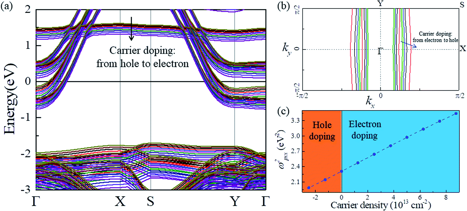 | ||
| Fig. 3 Carrier tunable electronic properties of monolayer NaW2O2Br6. (a) Band structures under carrier doping from −2.5 × 1013 cm−2 (hole) to 8.75 × 1013 cm−2 (electron). (b) The Fermi surfaces with the carrier doping concentration of −2.5 (red), 0 (black), 2.5 (blue), 5.0 (green), and 7.5 (olive) × 1013 cm−2, respectively. (c) The dependence of ωp2 on carrier doping concentration. | ||
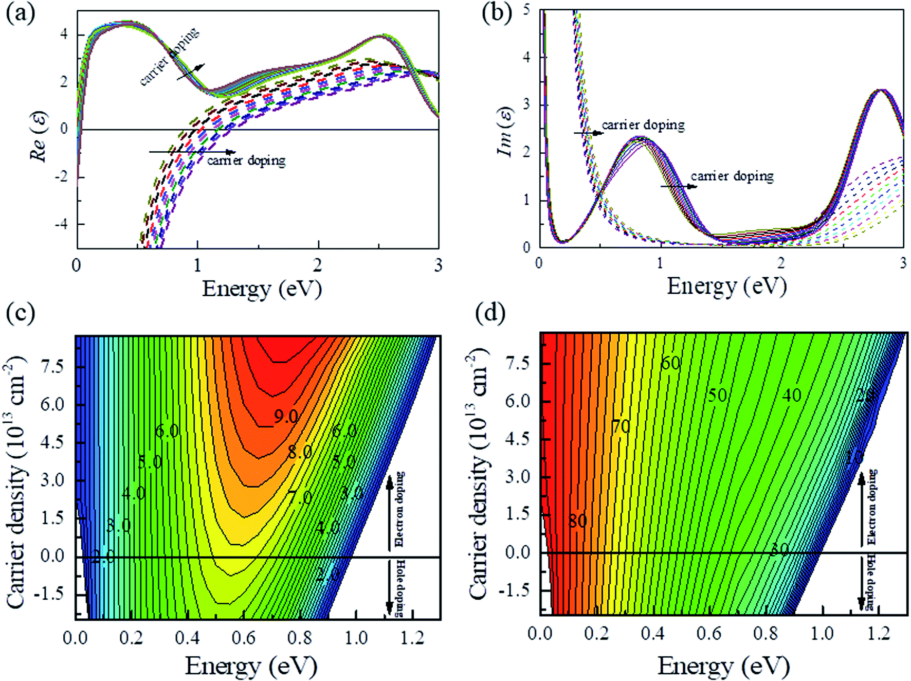 | ||
| Fig. 4 Tunable hyperbolic properties of monolayer NaW2O2Br6 upon carrier density. (a and b) The real and imaginary parts of dielectric functions of monolayer NaW2O2Br6 upon carrier doping, respectively. The arrows indicate the carrier doping from holes to electrons. (c and d) The counter mapping of FoM and propagation direction (respect to the y axis) of the plasmon beams upon carrier doping, respectively. | ||
For hyperbolic optical devices, except the hyperbolic windows, other properties are also very important for applications, such as FoM and the propagation direction of the plasmon beams. The FoM upon the carrier density of monolayer NaW2O2Br6 is plotted in Fig. 4c. The color region is hyperbolic, while the other region is elliptic. We found that the highest FoM can be enhanced and gradually blueshifted with the electron doping. The best FoM is about 7.3 at 0.56 eV without doping, and it increases to about 9.9 at 0.75 eV with an electron doping concentration of 8.75 × 1013 cm−2. Interestingly, although it is hyperbolic from FIR to NIR, the tunability upon carrier density is different. As shown in Fig. 4c, below about 0.4 eV, the FoM is not sensitive to carrier concentration. In the range between 0.4 and 0.88 eV, increasing the electron density would significantly improve the FoM. Above 0.88 eV, the topological transition between elliptic and hyperbolic can occur, and the FoM can also be dramatically enhanced. As we see, it is elliptic at 0.9 eV with a hole doping concentration of 2.5 × 1013 cm−2. It changes to hyperbolic with the FoM quickly increasing to 9.0 at an electron doping concentration of 8.75 × 1013 cm−2. Thus, although the hyperbolic window can cover almost the whole IR light, only NIR light can be tuned by carrier density, not FIR and MIR light.
Similar tunable behavior is also found for the direction of the plasmon beams. In the hyperbolic range, the plasmon beams are significantly more localized than the elliptic case, because plasmons with all momenta carry energy along the direction of the hyperbola asymptotes defined by18
 | (4) |
Usually, the direction of the plasmon beams is also defined by the direction of asymptotes. Fig. 4d displays the propagation directions of plasmon beams by the angle between the y axis and plasmon beams. As we see, the propagation directions of MIR and FIR lights are mainly restrained along the x direction, and they show little dependence on carrier density. For NIR light above 0.4 eV, its propagation directions can be controlled by carrier density. For example, the angle can be rotated from 40° to 54° for the light of 0.6 eV, when the doped carrier concentration changes from holes of 2.5 × 1013 cm−2 to electrons of 8.75 × 1013 cm−2. Above 0.9 eV, the propagation directions of plasmon beams can also be tuned when the topology transition between elliptic and hyperbolic occurs. This indicates that carrier concentration not only can control the hyperbolic window and their FoMs, but also can control the propagation behaviors.
These tunable hyperbolic properties are due to the extremely anisotropic electronic properties in monolayer NaW2O2Br6. Interestingly, we also found that the tunable behavior upon carrier concentration is also extremely anisotropic. By the dielectric properties, including Im(ε) and Re(ε), shown in Fig. 4a and b, the absorption peaks around 0.9 eV and 2.7 eV for the y direction are nearly independent of the carrier concentration. The absorption peak around 0.9 eV is due to the interband transitions from the dxz (dxy) orbital below the Fermi level to the dxy (dxz) orbital above the Fermi level, as illustrated in Fig. 2a. Shifting the Fermi level by carrier concentration has a negligible effect on this transition. It is similar for the absorption peaks around 2.7 eV. But in the x direction, the optical transitions from the dxz (dxy) orbital below the Fermi level to the dxy (dxz) orbital are optically forbidden. The absorption starting from 2.0 eV for the x direction is due to the interband transition from bands around −2 eV to the bands above the Fermi level. This interband transition is carrier dependent in a mechanism like the Burstein–Moss effect. Such extremely anisotropic properties, especially the anisotropic tunable behavior, are never reported in other materials, endowing monolayer NaW2O2Br6 with particular potential in electrically controlling directional optical devices.
Tunable hyperbolic PPs by solid-gated FETs
From the perspective of potential applications, the ability to integrate hyperbolic PhPs into nanophotonic and optoelectronic circuits is highly desirable. Based on the first-principles calculations, a carrier density at the order of 1013 cm−2 can effectively modulate the hyperbolic performance in monolayer NaW2O2Br6, including the hyperbolic window, FoM and the propagation direction of plasmon beams. Such carrier density usually can be easily realized in electric double layer transistors (EDLTs)34,35 by using polymer electrolytes or ionic liquids as gated dielectrics. But EDLTs are not feasible for integrating these hyperbolic properties into nano-optoelectronic devices. Luckily, it is reported that such carrier density could also be approached in some well-fabricated solid-gated FETs,36,37 which makes a possibility for the design of gate tunable hyperbolic photonic devices. Thus, we propose a gate tunable hyperbolic device based on solid-gated FETs with monolayer NaW2O2Br6 as the channel. The schematic device is shown in Fig. 5, where the bottom gate supplies the electric field to control the propagation behaviors of NIR light in monolayer NaW2O2Br6. According to the calculations, when a NIR light propagates in monolayer NaW2O2Br6, the propagation direction, the FoM, and even the topology (elliptic and hyperbolic) of NIR light can be controlled by the gate voltage, depending on the light wavelength. The ability to integrate with FETs enables electrical control of optical signals in monolayer NaW2O2Br6, which has significant implications on integrating photonics and nano-optoelectronics into a single chip and also other novel optoelectronic devices. For example, hyperbolic PPs can support the plasmonic spin-Hall effect.38 In the range of (0.88, 1.27) eV, it is hyperbolic or elliptic depending on the carrier density, i.e., the gate voltage. It means that the plasmonic spin-Hall effect for NIR light can be switched by the gate voltage in monolayer NaW2O2Br6.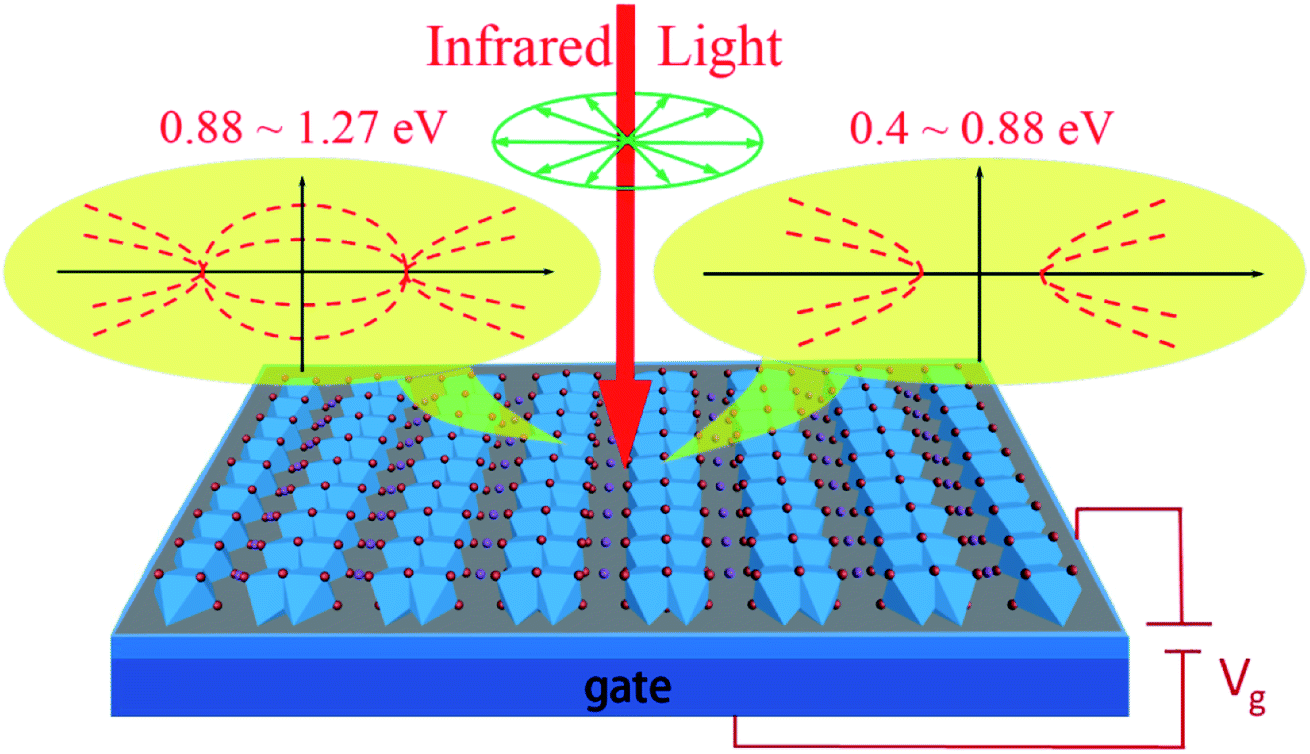 | ||
| Fig. 5 Schematic diagram of the gate tunable NIR hyperbolic device by FETs. When a NIR incident light illuminated on monolayer NaW2O2Br6, the propagation behaviors of NIR light in monolayer NaW2O2Br6, including the propagation direction, the FoM, and even the topology (depending on the wavelength of NIR light), can be manipulated by the gate voltage. | ||
As we discussed above, the hyperbolic PPs in monolayer NaW2O2Br6 are mainly due to the extremely anisotropic electronic properties. Except the electronic properties, the tunability in optical properties upon carrier density is also extremely anisotropic, indicating that other properties in monolayer NaW2O2Br6, such as mechanic, transport, and thermal properties, could also be extremely anisotropic. For example, the thermal conductivity as known is contributed by both phonons and electrons. In monolayer NaW2O2Br6, it is conducting for the y direction but almost insulating for the x direction, suggesting the extremely anisotropic thermal conductivity from electron contribution. Such extremely anisotropic properties in monolayer NaW2O2Br6 would also open opportunities for novel functional anisotropic devices.
In conclusion, we propose that monolayer NaW2O2Br6 is a natural candidate for infrared hyperbolic PPs with extraordinary properties, such as broad hyperbolic window and considerable FoM, because of its extremely anisotropic structural and metallic properties. Owing to the low intrinsic carrier concentration, hyperbolic PPs in monolayer NaW2O2Br6 for NIR light can be manipulated by the gate voltage in solid-gated FETs, which provides great potential for application in integrating tunable polaritons into nano-optoelectronic devices. We anticipate our work will promote more experimental and theoretical efforts on the realization of integrable hyperbolic PPs based on 2D materials.
Methods
Electronic calculation for monolayer NaW2O2Br6
The electronic and dielectric properties of monolayer NaW2O2Br6 are calculated by the Vienna ab initio Simulation Package (VASP)39,40 based on density functional theory (DFT). The electronic structures are described by using the generalized gradient approximation (GGA) based Perdew–Burke–Ernzerhof (GGA-PBE) exchange–correlation functional41 with the projector augmented wave (PAW).42 The cutoff energy used for the plane-wave basis set is 450 eV for monolayer NaW2O2Br6. The structures are relaxed until the atomic forces are less than 0.01 eV per Å per atom and total energies are converged to 10−5 eV. Vacuum layers of 15 Å are inserted between the periodically repeated slabs along the c-axis to avoid interactions among them caused by the periodic boundary conditions for both. The PBE exchange–correlation functional usually underestimates both band gaps of semiconductors and interband transition energies in metals. We applied a hybrid functional (HSE06)43 to compute the electronic structures of monolayer NaW2O2Br6, which generally yields more reliable band energies. Finer k-point samplings of 80 × 30 × 1 are used to calculate FSs.Dielectric calculation for monolayer NaW2O2Br6
We apply the independent particle approximation to describe the dielectric function from electronic band structure calculations. The dielectric function ε(ω) = ε1(ω) + iε2(ω) (where ε1 is the real part, and ε2 is the imaginary part) of metals in the low-frequency region is contributed by two important processes, interband (εinter(ω)) and intraband (εintra(ω)) transitions.The imaginary part of the dielectric function contributed by interband transition is calculated by44
 | (5) |
The dielectric function for intraband transitions, εintra(ω), is known as the dielectric function of a free electron gas. The contribution by intraband transitions, εintra(ω), is obtained by Drude expression for a given plasma frequency ωp and damping constant (γ):31
 | (6) |
 | (7) |
Dense k-point samplings of 100 × 40 × 1 are applied to calculate the dielectric properties of monolayer NaW2O2Br6. The total dielectric function is the sum of the dielectric functions for inter- and intraband transitions: ε(ω) = εinter(ω) + εintra(ω).
Conflicts of interest
The authors declare no competing interests.Acknowledgements
B. X. acknowledges the support from “Double First-Class” University project of China Pharmaceutical University (CPU2018GFY25).References
- D. N. Basov, M. M. Fogler and F. J. G. de Abajo, Polaritons in van der Waals materials, Science, 2016, 354, 1992 CrossRef PubMed.
- T. Low, A. Chaves, J. D. Caldwell, A. Kumar, N. X. Fang, P. Avouris, T. F. Heinz, F. Guinea, L. Martin-Moreno and F. Koppens, Polaritons in layered two-dimensional materials, Nat. Mater., 2017, 16, 182–194 CrossRef CAS PubMed.
- Q. Zhang, G. W. Hu, W. L. Ma, P. N. Li, A. Krasnok, R. Hillenbrand, A. Alu and C. W. Qiu, Interface nano-optics with van der Waals polaritons, Nature, 2021, 597, 187–195 CrossRef CAS PubMed.
- A. Woessner, M. B. Lundeberg, Y. Gao, A. Principi, P. Alonso-Gonzaolez, M. Carrega, K. Watanabe, T. Taniguchi, G. Vignale, M. Polini, J. Hone, R. Hillenbrand and F. H. L. Koppens, Highly confined low-loss plasmons in graphene-boron nitride heterostructures, Nat. Mater., 2015, 14, 421–425 CrossRef CAS PubMed.
- P. N. Li, I. Dolado, F. J. Alfaro-Mozaz, F. Casanova, L. E. Hueso, S. Liu, J. H. Edgar, A. Y. Nikitin, S. Velez and R. Hillenbrand, Infrared hyperbolic metasurface based on nanostructured van der Waals materials, Science, 2018, 359, 892–896 CrossRef CAS PubMed.
- S. Dai, Z. Fei, Q. Ma, A. S. Rodin, M. Wagner, A. S. McLeod, M. K. Liu, W. Gannett, W. Regan, K. Watanabe, T. Taniguchi, M. Thiemens, G. Dominguez, A. H. Castro Neto, A. Zettl, F. Keilmann, P. Jarillo-Herrero, M. M. Fogler and D. N. Basov, Tunable Phonon Polaritons in Atomically Thin van der Waals Crystals of Boron Nitride, Science, 2014, 343, 1125–1129 CrossRef CAS PubMed.
- W. L. Ma, P. Alonso-Gonzalez, S. J. Li, A. Y. Nikitin, J. Yuan, J. Martin-Sanchez, J. Taboada-Gutierrez, I. Amenabar, P. N. Li, S. Velez, C. Tollan, Z. G. Dai, Y. P. Zhang, S. Sriram, K. Kalantar-Zadeh, S. T. Lee, R. Hillenbrand and Q. L. Bao, In-plane anisotropic and ultra-low-loss polaritons in a natural van der Waals crystal, Nature, 2018, 562, 557–562 CrossRef CAS PubMed.
- G. W. Hu, Q. D. Ou, G. Y. Si, Y. J. Wu, J. Wu, Z. G. Dai, A. Krasnok, Y. Mazor, Q. Zhang, Q. L. Bao, C. W. Qiu and A. Alu, Topological polaritons and photonic magic angles in twisted alpha-MoO3 bilayers, Nature, 2020, 582, 209–213 CrossRef CAS PubMed.
- Z. B. Zheng, N. S. Xu, S. L. Oscurato, M. Tamagnone, F. S. Sun, Y. Z. Jiang, Y. L. Ke, J. N. Chen, W. C. Huang, W. L. Wilson, A. Ambrosio, S. Z. Deng and H. J. Chen, A mid-infrared biaxial hyperbolic van der Waals crystal, Sci. Adv., 2019, 5, eaav8690 CrossRef CAS PubMed.
- Q. Zhang, Q. D. Ou, G. W. Hu, J. Y. Liu, Z. G. Dai, M. S. Fuhrer, Q. L. Bao and C. W. Qiu, Hybridized hyperbolic surface phonon polaritons at alpha-MoO3 and polar dielectric interfaces, Nano Lett., 2021, 21, 3112–3119 CrossRef CAS PubMed.
- J. Taboada-Gutierrez, G. Alvarez-Perez, J. H. Duan, W. L. Ma, K. Crowley, I. Prieto, A. Bylinkin, M. Autore, H. Volkova, K. Kimura, T. Kimura, M. H. Berger, S. J. Li, Q. L. Bao, X. P. A. Gao, I. Errea, A. Y. Nikitin, R. Hillenbrand, J. Martin-Sanchez and P. Alonso-Gonzalez, Broad spectral tuning of ultra-low-loss polaritons in a van der Waals crystal by intercalation, Nat. Mater., 2020, 19, 964–968 CrossRef CAS PubMed.
- A. N. Grigorenko, M. Polini and K. S. Novoselov, Graphene plasmonics, Nat. Photonics, 2012, 6, 749–758 CrossRef CAS.
- Z. Fei, A. S. Rodin, G. O. Andreev, W. Bao, A. S. McLeod, M. Wagner, L. M. Zhang, Z. Zhao, M. Thiemens, G. Dominguez, M. M. Fogler, A. H. Castro Neto, C. N. Lau, F. Keilmann and D. N. Basov, Gate-tuning of graphene plasmons revealed by infrared nano-imaging, Nature, 2012, 487, 82–85 CrossRef CAS PubMed.
- G. X. Ni, A. S. McLeod, Z. Sun, L. Wang, L. Xiong, K. W. Post, S. S. Sunku, B. Y. Jiang, J. Hone, C. R. Dean, M. M. Fogler and D. N. Basov, Fundamental limits to graphene plasmonics, Nature, 2018, 557, 530–533 CrossRef CAS PubMed.
- J. S. Gomez-Diaz and A. Alu, Flatland optics with hyperbolic metasurfaces, ACS Photonics, 2016, 3, 2211–2224 CrossRef CAS.
- J. S. Gomez-Diaz, M. Tymchenko and A. Alu, Hyperbolic plasmons and topological transitions over uniaxial metasurfaces, Phys. Rev. Lett., 2015, 114, 233901 CrossRef PubMed.
- C. Wang, S. Y. Huang, Q. X. Xing, Y. G. Xie, C. Y. Song, F. J. Wang and H. G. Yan, Van der Waals thin films of WTe2 for natural hyperbolic plasmonic surfaces, Nat. Commun., 2020, 11, 1158 CrossRef CAS PubMed.
- Z. Torbatian, D. Novko and R. Asgari, Tunable Low-Loss Hyperbolic Plasmon Polaritons in a Td-WTe2 Single Layer, Phys. Rev. Appl., 2020, 14, 044014 CrossRef CAS.
- A. Nemilentsau, T. Low and G. Hanson, Anisotropic 2D materials for tunable hyperbolic plasmonics, Phys. Rev. Lett., 2016, 116, 066804 CrossRef PubMed.
- E. Veen, A. Nemilentsau, A. Kumar, R. Roldan, M. I. Katsnelson, T. Low and S. J. Yuan, Tuning two-dimensional hyperbolic plasmons in black phosphorus, Phys. Rev. Appl., 2019, 12, 014011 CrossRef.
- J. A. Silva-Guillen, E. Canadell, F. Guinea and R. Roldan, Strain tuning of the anisotropy in the optoelectronic properties of TiS3, ACS Photonics, 2018, 5, 3231–3237 CrossRef CAS.
- Y. F. Huang, S. N. Shirodkar and B. I. Yakobson, Two-dimensional boron polymorphs for visible range plasmonics: A first-principles exploration, J. Am. Chem. Soc., 2017, 139, 17181–17185 CrossRef CAS PubMed.
- C. Lian, S. Q. Hu, J. Zhang, C. Cheng, Z. Yuan, S. W. Gao and S. Meng, Integrated plasmonics: broadband dirac plasmons in borophene, Phys. Rev. Lett., 2020, 125, 116802 CrossRef CAS PubMed.
- J. Z. Zhao, W. K. Wu, J. J. Zhu, Y. H. Lu, B. Xiang and S. Y. A. Yang, Highly anisotropic two-dimensional metal in monolayer MoOCl2, Phys. Rev. B: Condens. Matter Mater. Phys., 2020, 102, 245419 CrossRef CAS.
- W. H. Geng, H. Gao, C. Ding, L. Sun, X. K. Ma, Y. Y. Li and M. W. Zhao, Highly-anisotropic plasmons in two-dimensional hyperbolic copper borides, Opt. Express, 2022, 30, 5596–5607 CrossRef CAS PubMed.
- Y. Q. Zheng, K. Peters and H. G. von Schnering, The mixed valence tungsten(IV,V) compound Na[W2O2Br6], Z. Anorg. Allg. Chem., 1998, 624, 1415–1418 CrossRef CAS.
- K. Andersen and K. S. Thygesen, Plasmons in metallic monolayer and bilayer transition metal dichalcogenides, Phys. Rev. B: Condens. Matter Mater. Phys., 2013, 88, 155128 CrossRef.
- A. Poddubny, I. Iorsh, P. Belov and Y. Kivshar, Hyperbolic metamaterials, Nat. Photonics, 2013, 7, 948–957 CrossRef CAS.
- D. Hirai, M. Bremholm, J. M. Allred, J. Krizan, L. M. Schoop, Q. Huang, J. Tao and R. J. Cava, Spontaneous formation of zigzag chains at the metal-insulator transition in the beta-pyrochlore CsW2O6, Phys. Rev. Lett., 2013, 110, 166402 CrossRef PubMed.
- K. N. Zhang, X. Y. Liu, H. X. Zhang, K. Deng, M. Z. Yan, W. Yao, M. T. Zheng, E. F. Schwier, K. Shimada, J. D. Denlinger, Y. Wu, W. H. Duan and S. Y. Zhou, Evidence for a quasi-one-dimensional charge density wave in cuTe by angle-resolved photoemission spectroscopy, Phys. Rev. Lett., 2018, 121, 206402 CrossRef CAS PubMed.
- S. A. Maier, Plasmonics, Fundamentals and Applications, Springer, 2007, vol. 26, p. 224 Search PubMed.
- K. H. Lee and K. J. Chang, First-principles study of the optical properties and the dielectric response of Al, Phys. Rev. B: Condens. Matter Mater. Phys., 1994, 49, 2362–2367 CrossRef CAS PubMed.
- R. A. Maniyara, D. Rodrigo, R. Yu, J. Canet-Ferrer, D. S. R. Ghosh, R. Yongsunthon, D. E. Baker, A. Rezikyan, F. J. G. de Abajo and V. Pruneri, Tunable plasmons in ultrathin metal films, Nat. Photonics, 2019, 13, 328–333 CrossRef CAS.
- D. Braga, I. G. Lezama, H. Berger and A. F. Morpurgo, Quantitative determination of the band gap of WS2 with ambipolar ionic liquid-gated transistors, Nano Lett., 2012, 12, 5218–5223 CrossRef CAS PubMed.
- D. K. Efetov and P. Kim, Controlling electron-phonon interactions in graphene at ultrahigh carrier densities, Phys. Rev. Lett., 2010, 105, 256805 CrossRef PubMed.
- Y. J. Zhang, J. T. Ye, Y. Matsuhashi and Y. Iwasa, Ambipolar MoS2 Thin Flake Transistors, Nano Lett., 2012, 12, 1136–1140 CrossRef CAS PubMed.
- K. F. Mak, K. L. He, C. Lee, G. H. Lee, J. Hone, T. F. Heinz and J. Shan, Ambipolar MoS2 thin flake transistors, Nat. Mater., 2013, 12, 207–211 CrossRef CAS PubMed.
- A. A. High, R. C. Devlin, A. Dibos, M. Polking, D. S. Wild, J. Perczel, N. P. de Leon, M. D. Lukin and H. Park, Visible-frequency hyperbolic metasurface, Nature, 2015, 522, 192–196 CrossRef CAS PubMed.
- G. Kresse and J. Hafner, Ab initio molecular dynamics for open-shell transition metals, Phys. Rev. B: Condens. Matter Mater. Phys., 1993, 48, 13115 CrossRef CAS PubMed.
- G. Kresse and J. Furthmuller, Efficient iterative schemes for ab initio total-energy calculations using a plane-wave basis set, Phys. Rev. B: Condens. Matter Mater. Phys., 1996, 54, 11169 CrossRef CAS PubMed.
- J. P. Perdew, K. Burke and M. Ernzerhof, Generalized gradient approximation made simple, Phys. Rev. Lett., 1996, 77, 3865 CrossRef CAS PubMed.
- P. E. Blochl, Projector augmented-wave method, Phys. Rev. B: Condens. Matter Mater. Phys., 1994, 50, 17953 CrossRef PubMed.
- J. Heyd, G. E. Scuseria and M. Ernzerhof, Hybrid functionals based on a screened Coulomb potential, J. Chem. Phys., 2003, 118, 8207–8215 CrossRef CAS.
- M. Gajdos, K. Hummer, G. Kresse, J. Furthmuller and F. Bechstedt, Linear optical properties in the projector-augmented wave methodology, Phys. Rev. B: Condens. Matter Mater. Phys., 2006, 73, 045112 CrossRef.
Footnotes |
| † Electronic supplementary information (ESI) available. See https://doi.org/10.1039/d2na00292b |
| ‡ These authors contributed equally: Enhui Huang, and Hui Xiang. |
| This journal is © The Royal Society of Chemistry 2022 |