
 Open Access Article
 This Open Access Article is licensed under a Creative Commons Attribution-Non Commercial 3.0 Unported Licence
Nanoscale heat transport analysis by scanning thermal microscopy: from calibration to high-resolution measurements†
Liliana
Vera-Londono
 a,
Alejandra
Ruiz-Clavijo
a,
Jaime Andrés
Pérez-Taborda
ab and
Marisol
Martín-González
*a
a,
Alejandra
Ruiz-Clavijo
a,
Jaime Andrés
Pérez-Taborda
ab and
Marisol
Martín-González
*a
aInstituto de Micro y Nanotecnología, IMN-CNM, CSIC (CEI UAM+CSIC) Isaac Newton, 8, Tres Cantos, E-28760, Madrid, Spain. E-mail: marisol.martin@csic.es
bUniversidad Nacional de Colombia Sede De La Paz, Escuela de Pregrados-Dirección Académica – Vicerrectoría, Grupo de Nanoestructuras y Física Aplicada (NANOUPAR), Km 9 vía Valledupar La Paz, La Paz 202010, Colombia
First published on 22nd June 2022
Abstract
Scanning thermal microscopy (SThM) is a powerful technique for thermal characterization. However, one of the most challenging aspects of thermal characterization is obtaining quantitative information on thermal conductivity with nanoscale lateral resolution. We used this technique with the cross-point calibration method to obtain the thermal contact resistance, Rc, and thermal exchange radius, b, using thermo-resistive Pd/Si3N4 probes. The cross-point curves correlate the dependence of Rc and b with the sample's thermal conductivity. We implemented a 3ω-SThM method in which reference samples with known thermal conductivity were used in the calibration and validation process to guarantee optimal working conditions. We achieved values of Rc = 0.94 × 10⁶ ± 0.02 K W−1 and b = 2.41 × 10⁻⁷ ± 0.02 m for samples with a low thermal conductivity (between 0.19 and 1.48 W m−1 K−1). These results show a large improvement in spatial resolution over previously reported data for the Wollaston probes (where b ∼ 2.8 μm). Furthermore, the contact resistance with the Pd/Si3N4 is ∼20× larger than reported for a Wollaston wire probe (with 0.45 × 10⁵ K W−1). These thermal parameters were used to determine the unknown thermal conductivity of thermoelectric films of Ag2Se, Ag2−xSe, Cu2Se (smooth vs. rough surface), and Bi2Te3, obtaining, in units of W m−1 K−1, the values of 0.63 ± 0.07, 0.69 ± 0.15, 0.79 ± 0.03, 0.82 ± 0.04, and 0.93 ± 0.12, respectively. To the best of our knowledge, this is the first time these microfabricated probes have been calibrated using the cross-point method to perform quantitative thermal analysis with nanoscale resolution. Moreover, this work shows high-resolution thermal images of the V1ω and V3ω signals, which can offer relevant information on the material's heat dissipation.
1. Introduction
Scientific and technological breakthroughs in nanomaterials research and manufacturing engineering are often directly linked to advances in characterization techniques.1 Characterizing the material's properties makes it possible to establish a connection between physical properties, size's material changes, confinement effects, or variation of the chemical composition, among others.2–5 It has facilitated the development of new applications in solid-state thermal management, energy storage, thermoelectricity, electronics, and photonics systems.6–11Specifically, when the size of the material is reduced from 3D (bulk-type) to 2D (thin film, bilayers, and monolayers), 1D (nanotubes and nanowires), or 0D (quantum dots and nanoparticles),12,13 the heat transport across the structure could deviate from classical Fourier's law. Size's material reduction can induce particle confinement, which involves an increment of the phonon scattering events, that may provoke a reduction in the material's thermal conductivity (κ). This reduction of κ is of utmost importance in many applications. For example, in the case of thermoelectricity, the efficiency (zT) of the materials is inversely proportional to κ, since zT = S2σTκ−1, where S is the Seebeck coefficient, σ is the electrical conductivity, and T is the absolute temperature. However, the heat transport measurements in nanoscale structures, such as micro and nanocomposites, nanomeshes, nanowires, or nanotubes, are always challenging.14–17 Spatially resolved techniques that enable obtaining thermal information of the material with a resolution at the micro and nanoscale are highly desired. Different techniques have been reported in the literature to determine the thermal conductivity of bulk and nanostructured materials. The most popular ones are Raman spectroscopy,18 laser flash (LF),19 or time-domain thermoreflectance (TDTR).20 Nevertheless, the techniques mentioned above do not have enough thermal resolution or require a preparation that might cause sample damage. Alternatively, a technique for determining thermal conductivity and overcoming the above limitations is the scanning thermal microscopy (SThM).21 This technique uses a thermal probe to obtain a thermal map of the sample surface.22–24
While different SThM measuring methods can be used, we will mainly focus on the 3ω-SThM mode. This method works with thermo-resistive probes, whose electrical resistance depends on the probe's temperature. An alternating voltage or current (AC) is applied to a thermal probe, and the flow of current through the probe will induce self-heating at the tip because of the Joule effect. When this tip scans in contact mode the surface of a sample with different thermal conductivities, the heat exchange between the sample and the probe causes temperature variations in the tip. Fluctuations in the first harmonic signal (1ω) induce resistance changes that will be observed as a second harmonic frequency (2ω), producing a voltage variation in the third harmonic frequency (3ω). Voltage changes at frequencies of 1ω, V1ω, and 3ω, V3ω, are measured by a Wheatstone bridge and a lock-in system, similarly to ref. 25 The total heat flow across the system is:
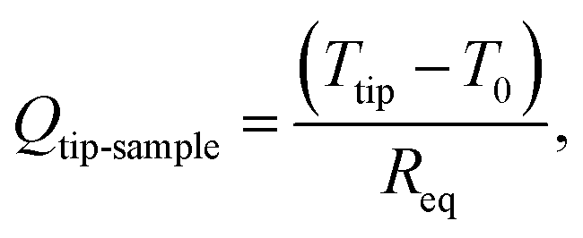 | (1) |
| Req = Rc + Rs, | (2) |
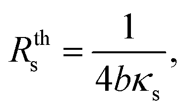 | (3) |
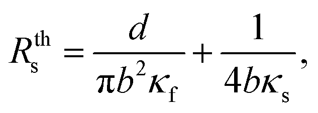 | (4) |
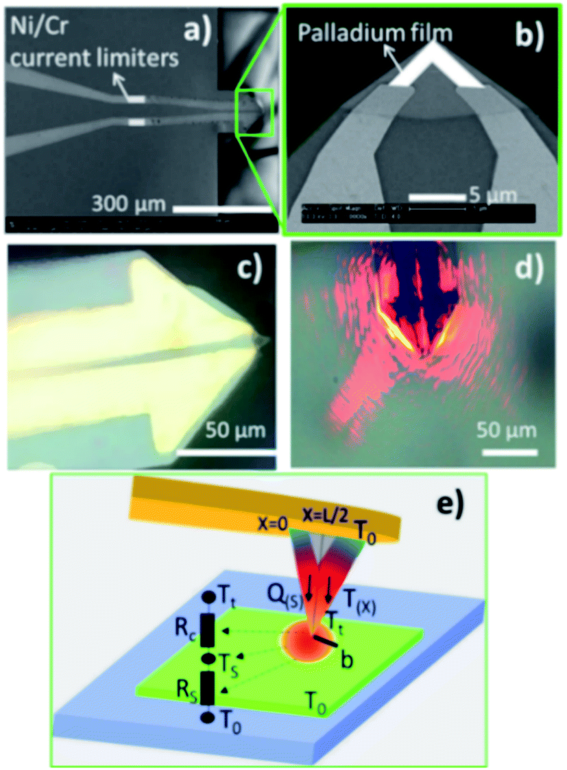 | ||
| Fig. 1 (a) SEM micrographs of the microfabricated thermal probe used in this experiment and (b) zoom-in of the tip apex, where the palladium film coating the tip is observed. Optical images of the probe to the atomic force microscopy (AFM) station with the laser off in (c) and laser on in (d). The diagram of the thermal resistance network and the thermal interaction between probe and sample are shown in (e). | ||
This work shows a calibration method with Pd/Si3N4 probes to get the contact resistance Rc analytically as a function of the thermal radius “b” from a set of well-known thermal conductivity samples. This method is called cross-point calibration and typically works for a set of samples with specific thermal conductivity ranges, as reported by Wilson et al. in ref. 27. Based on his work27 but using microfabricated probes instead of Wollaston wire, we determine Rc and b accurately through cross-point calibration. One of the most important aspects that should be highlighted in this paper is the advantage of our method to obtain the high-resolution SThM images of different types of samples. We used reference samples with known κ to calibrate the probe-sample interaction and cross-checked the results with test samples to ensure reliable measurements. Furthermore, we determine κ in selected samples from some of the most representative families in thermoelectric (TE) materials, such as films of silicon-germanium, bismuth telluride, and silver and copper selenides. These films are semiconductors materials of great interest to be used from room temperature to high temperature in different TE applications and microelectronic devices. Measurements were performed with 3ω-SThM for samples with low thermal conductivity between 0.19 W m−1 K−1 and 1.48 W m−1 K−1. This paper presents an experimental configuration with a modified lab-made Wheatstone bridge to acquire high-quality SThM images utilizing the cross-point method with the microfabricated probes. This method allows us to determine κ in nanostructured samples with different features. We are confident that these results can contribute to the qualitative and quantitative thermal transport analysis of materials at the micro and nanoscale.
2. Experiment details
2.1 Experimental set-up
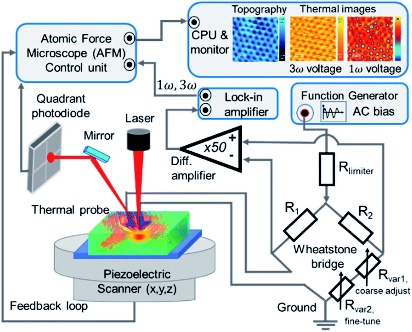
The SThM measurements were performed using a Nanotec Electronica® atomic force microscope (AFM) to approach and scan the sample surface with a Pd/Si3N4 probe—model VITA-DM-GLA-1 from Bruker®. One of the fundamental characteristics of this type of probe, is that it has a coating film of palladium (Pd) at the tip. The Pd film is a thermo-resistive element that acts as a heater and thermometer during the measurements. It is called the active mode of SThM measurements. Furthermore, as explained in the introduction, this probe is heated up by an alternating voltage (AC), which offers advantages over direct current (DC) like reducing the heat loss in the probe. The probe is connected to a balanced Wheatstone bridge circuit. The probe is in contact with the sample surface, where different thermal parameters control the heat exchange from the heated probe to the sample. These are the sample's thermal conductivity, the thermal contact area, and the temperature variations at the probe and sample. The experimental setup configuration keeps constant the last two parameters. Therefore, the sample's thermal conductivity is the only parameter that causes heat flow changes. However, if the sample's thermal conductivity varies, the probe's temperature varies too, which leads to a probe's resistance changes. Consequently, a voltage difference appears in the balanced bridge, initially adjusted to have zero potential difference between two output points. Then, the feedback loop detects the voltage shift in the balanced bridge to restore the probe's temperature or resistance, depending on whether it operates at constant temperature or constant current. In this experiment, we use SThM working in active mode, also called conductivity contrast mode (CCM), at a constant current.22,28A lab-made Wheatstone bridge was employed to control the supply voltage as a current source and to detect slight voltage changes. Furthermore, we obtained thermal images with improvements in contrast and resolution by optimizing the bridge design and the electronic circuit connection. See details of this Wheatstone bridge in ESI (Fig. S.I.1 and S.I.2†). An ultra-high-frequency lock-in amplifier, UHFLI 600 MHz from Zurich Instruments®, operated with the control software LabOne, is used to perform the feedback loop. It collects the slight fluctuations of the voltage output in the bridge after passing by a pre-amplifier system, model 5113 low noise voltage preamplifier from AMETEK Scientific Instruments®. The probe was mounted in the AFM in a specially lab-designed cantilever holder, as shown in Fig. S.I.4.d in ESI.† The harmonic signal outputs from the lock-in system were connected to the AFM control unit. The acquired signals correspond to the generated harmonic voltages across the probe, the first, the second, and the third harmonics voltages, which are V1ω, V2ω, and V3ω, respectively. The topographic and thermal images of the sample were obtained simultaneously in the AFM. The images were processed using the WSxM software.29 The representative scheme of the experimental setup is shown in Fig. 2.
 | ||
| Fig. 2 Scheme of the experimental setup of 3ω-SThM, where the V3ω and V1ω were acquired. | ||
In addition to the characterization of the thermal conductivity carried out by SThM, different techniques were used to characterize the structural and physical–chemical properties of the samples. X-ray photoelectron spectroscopy (XPS) is used to determine the elemental composition and binding energies of silver selenide films.30 The XPS spectra were recorded at room temperature for the sample without heat treatment and after annealing at 200 °C. These measurements were done with a SPECS 100/150, with a polychromatic Al Kα radiation (photon energy = 1486.6 eV) in a 2-DLine detector energy pass of 50 eV and an electron take-off angle of 120°. High-resolution measurements were performed at 0.02 eV per step in each element of Ag and Se. The resolution, under these conditions, was 0.8 eV. The spectra were adjusted based on the carbon binding energy of C 1s = 284.6 eV. The CASA-XPS software of SEPCS was used to analyze the spectra. The difference of quantic levels in the 3d5/2 and 3d3/2 for the Ag and 3p3/2 and 3p1/2 for the Se was of ΔAg(3d5/2 − 3d3/2) = 6.0 eV and ΔSe(3p3/2 − 3p1/2) = 5.5 eV, respectively. The Ag2Se samples were analyzed with a scanning electron microscope (SEM) with electron-dispersive X-ray (EDX). In addition, all the samples were analyzed with SEM VERIOS 460 from FEI.
2.2 Heat transfer model
The authors in ref. 22 have already discussed the thermal transport model to extract the thermal conductivity with thermistor probes. This heat transfer model is based on a transient fin equation. The transient effects are typical in the classical 3ω method using the hot strip, as reported by Cahill et al. in ref. 31. However, due to the probe's size, the authors in ref. 32 did not observe transient behaviour. Instead, a stationary regime with appropriated boundary conditions could be assumed. Puyoo et al.33 reported a thermal model that includes the probe behaviour under ambient conditions in both out-of-contact and in-contact with the sample. The probe's cross-sectional area corresponding to the metallic Pd film (the heating element) was separated for the model. They identified the parameters dependent on the probe type that influenced the thermal model. Therefore, as the Pd/Si3N4 probe is heated with an AC signal, the current is defined as I(t) = I0![[thin space (1/6-em)]](https://www.rsc.org/images/entities/char_2009.gif) cos(ωt). The rise of the temperature amplitude due to Joule heating is proportional to the 3ω voltage of the tip as:
cos(ωt). The rise of the temperature amplitude due to Joule heating is proportional to the 3ω voltage of the tip as: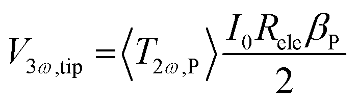 | (5) |
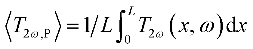 (where L is the tip length), I0 is the electrical current amplitude applied to the probe, Rele is the electrical resistance of the probe at the operating temperature, and βP is the probe temperature coefficient of the resistance. Then the power is defined as P = Iω2Rele, and the corresponding heat equation solved in the Fourier space is formulated in eqn (S.I.1) in ESI† As was described by Zhang et al.,34 the average temperature variation of the probe, ΔTprobe, in eqn (5) divided by the total power, P = VRMS × IRMS, gives the thermal probe resistance Rp. The thermal sample resistance (Req = Rc + Rs) can be calculated by fitting the heat flux of probe-to-sample from eqn (S.I.2†) to match the Rp in an appropriate ΔTprobe. The average temperature variation along the probe is obtained by solving the heat eqn (S.I.1)† giving a temperature profile. The heat transfer from the tip to the sample is characterized by a hot disc (b) with constant temperature distribution for uniform samples. The parameters Rc and b are constants and are independent of the sample's thermal conductivity within a specific range of conductivities. Therefore, the probe temperature is assumed to be constant in the region covering L/2 − b ≤ x ≤ L/2 (i.e., from the center of the tip to the L/2, where L is the total length of the v-shaped tip),33 providing the tip temperature. The heat transfer model is programmed in MATLAB®. The thermal, electrical, and geometrical parameters displayed in equations from (1) to (5) and equations from (S.I.1) to (S.I.4),† were fixed in the code routine. The model includes characteristics of the Pd/Si3N4 probes to fit the experimental data, like their geometry and shape and their thermal and electrical conductivity values for the palladium film. Additionally, it includes parameters for probe-sample configuration when out of contact and in contact modes, as the convective coefficient and the cut-off frequencies. The model also needs constants related to the used instrumentation, i.e., signal phases and gains from the signal generator, the preamplifier, and the amplifier system. See Table 1 with the main input parameters of the model and Section S.I.1† for more details on the heat transfer model.
| Components | Parameter Name | Symbol | Vacuum conditions | Atmospheric conditions | Value obtained |
|---|---|---|---|---|---|
| Pd/Si3N4 geometrical characteristics | Probe Si3N4 length | l p | (6.4–8.5) μm | Manufacturer specification/modelling | |
| Tip length Pd/Si3N4 | l t | (0.7–1.5) μm | Manufacturer specification/modelling | ||
| Probe thickness Si3N4 | t | (0.3–1) μm | Manufacturer specification/modelling | ||
| Section tip | s t | (lt × t) μm2 | Manufacturer specification/modelling | ||
| Perimeter Si3N4 + Pd | Per | 2·(lt + t) μm | Manufacturer specification/modelling | ||
| Pd/Si3N4 electrical properties | Electrical resistance of the probe | R p | (340–380) Ω | Measured | |
| Electrical resistance of Pd | R tip | (140–180) Ω | Manufacturer specification/modelling | ||
| Current amplitude of the probe | I p | (0.8–1.2) mA | Measured | ||
| Current limiter of NiCr to V3ω | G l | (0.01–0.04) V | (0.004–0.0069) V | Modelling | |
| Cut-off frequency | ω c | (800–1450) rad s−1 | (1500–3450) rad s−1 | Literature/modelling33 | |
| Pd/Si3N4 thermal properties | Thermal conductivity of Si3N4 | λ probe | (8.5–15) W m−1 K−1 | Manufacturer specification/modelling (depending on the probe thickness) | |
| Thermal diffusivity of Si3N4 | α probe | (1.2–2.2) μm2 s−1 | Manufacturer specification/modelling (depending on the probe thickness) | ||
| Pd temperature coefficient of resistance | TCRp | (1.1–1.3) e−3 K−1 | Literature/modelling33 | ||
| Heat transfer convection coefficient | h air | 0 | (13000–25000) W m−2 K−1 |
Literature/modelling35,36 | |
| Generator (distortion) | Modulus | V d | 0.00001 V | Modelling | |
| Phase | φ d | 5.0 rad | Modelling | ||
Although some of the parameters used to fit the experimental curves were previously measured or provided by the manufacturer, certain constants and values may be adjusted in the code (e.g., the convective heat coefficient, the preamplifier noise, voltage limiter). Also, determining the true contact area of the model can be more complex. Different contributions to the heat transfer should be considered, such as the transport due to air and the influence of water meniscus;37 but these mechanisms have been insignificant in this case. The conductance through water meniscus (Gwt), has already been calculated by Wilson A. in ref. 36 for microfabricated palladium probes Gwt, Pd ≈ 5.5 × 10⁻⁷ W K−1, which compared with solid–solid conduction is much lower. The contribution of radiative heat transfer (Grad) using the nominal probe geometry for Pd probes was also analyzed by Wilson A., finding conduction of Grad, Pd = 1.4 × 10⁻¹⁰ W K−1. The thermal radiation effects are negligible due to the small amplitude of AC temperature, as was pointed out by Borca-Tasciuc in ref. 26.
Regarding the temperature distribution in the tip, it has been widely discussed by Tovee et al. in ref. 38 and by Spiece et al. in ref. 39, that uniform distribution can be assumed in the case of a self-heated probe and for low thermal conductivity materials. As pointed out in ref. 38 and 39, when the tip is heated by the sample (passive mode) or is in contact with high thermal conductivity samples, the temperature drops occur at the very end of the tip. In these cases, the temperature distribution along the tip cannot be assumed as uniform. The analysis of high thermal conductivity samples with the current method would need modifications from the analytical and experimental points of view. Therefore, if the interest were to study a high thermal conductivity sample, this measurement probably will require new boundary conditions of the probe's temperature in the model and a vacuum system during sample measurements. That would be necessary to avoid miscalculations or distortion in the measurements due to the high heat transfer rates. However, these aspects are beyond the scope of this paper.
2.3. Calibration procedure and determination of thermal conductivity of different samples
 | (6) |
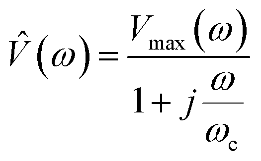
![[V with combining circumflex]](https://www.rsc.org/images/entities/i_char_0056_0302.gif) is the frequency dependency of the thermal signal, ωc = R−1 × C−1 is the cut-off frequency and Vmax is the amplitude of the 3ω signal. It is worth mentioning the importance of the cut-off frequency. The transfer function in eqn (6) has two operation modes in the frequency domain. Isothermal for frequencies <2ωc and adiabatic for frequencies >2ω. The ωc frequency is used as a reference to choose an appropriate excitation frequency ωe to heat the probe. Hence, the samples are scanned with the heated probe within the isothermal region if ωe< ωc. If the selected frequency is within the bandwidth of the probe response, the signal will be independent of the angular frequency and without thermal attenuation. In this region, the thermal response is not affected by changes in the heat capacity, as explained in ref. 33. After this first calibration of the probe (out of contact mode), we perform the second calibration with the probe-sample thermal interaction in contact mode. In this case, the sample must have a well-known thermal conductivity. This is done in atmospheric conditions by scanning the sample surface at one fixed electrical excitation frequency fe of 957 Hz, i.e., at angular frequency ωe(2πfe) of 6013 rad s−1. Since the probe behaves as a low-pass filter, it is known that its amplitude response will be reduced by 3 dB or attenuated by a factor of 70% after a cut-off frequency. The cut-off frequency determined for the Pd/Si3N4 probe was 16336 rad s−1. The excitation frequency is also conditioning the scan velocity to acquire the thermal signal. Puyoo et al. in ref. 25, reported that the time spent at each point when scanning with similar conditions is 5 ms. Compared with the 50 ms that can spend the Wollaston wires in each point, if the scan pixels are 256 × 256, the image acquisition with a microfabricated probe can take 6 minutes instead of the 60 minutes that takes the Wollaston wire probe. Here, with Pd/Si3N4 probes, image acquisition times vary between 6 to 22 minutes, depending on the points selection (i.e., 256 or 512). The velocity or lines per second (l per s) could be the highest at 0.98 l per s or the lowest value at 0.05 l per s, and the scan speed is linked to the image acquisition time. Thus, obtaining thermal and topographic images for one sample area (in the order of μm) may take over 25 minutes. The sweeping velocity was between 0.2 to 0.9 l per s, depending on the sample features and the scan size. Based on the parameters fitted to the probe's voltage response vs. excitation frequencies, the sigmoidal curves of V3ω response as a function of equivalent thermal resistance Req can be obtained (see Fig. 3b and d). Therefore, after scan a sample surface, the 3ω voltage of the sample can be correlated with Req of these curves. As explained in the introduction, if Req is known as well as Rc, b, then, sample's thermal conductivity can be determined (eqn (3) and (4)).
is the frequency dependency of the thermal signal, ωc = R−1 × C−1 is the cut-off frequency and Vmax is the amplitude of the 3ω signal. It is worth mentioning the importance of the cut-off frequency. The transfer function in eqn (6) has two operation modes in the frequency domain. Isothermal for frequencies <2ωc and adiabatic for frequencies >2ω. The ωc frequency is used as a reference to choose an appropriate excitation frequency ωe to heat the probe. Hence, the samples are scanned with the heated probe within the isothermal region if ωe< ωc. If the selected frequency is within the bandwidth of the probe response, the signal will be independent of the angular frequency and without thermal attenuation. In this region, the thermal response is not affected by changes in the heat capacity, as explained in ref. 33. After this first calibration of the probe (out of contact mode), we perform the second calibration with the probe-sample thermal interaction in contact mode. In this case, the sample must have a well-known thermal conductivity. This is done in atmospheric conditions by scanning the sample surface at one fixed electrical excitation frequency fe of 957 Hz, i.e., at angular frequency ωe(2πfe) of 6013 rad s−1. Since the probe behaves as a low-pass filter, it is known that its amplitude response will be reduced by 3 dB or attenuated by a factor of 70% after a cut-off frequency. The cut-off frequency determined for the Pd/Si3N4 probe was 16336 rad s−1. The excitation frequency is also conditioning the scan velocity to acquire the thermal signal. Puyoo et al. in ref. 25, reported that the time spent at each point when scanning with similar conditions is 5 ms. Compared with the 50 ms that can spend the Wollaston wires in each point, if the scan pixels are 256 × 256, the image acquisition with a microfabricated probe can take 6 minutes instead of the 60 minutes that takes the Wollaston wire probe. Here, with Pd/Si3N4 probes, image acquisition times vary between 6 to 22 minutes, depending on the points selection (i.e., 256 or 512). The velocity or lines per second (l per s) could be the highest at 0.98 l per s or the lowest value at 0.05 l per s, and the scan speed is linked to the image acquisition time. Thus, obtaining thermal and topographic images for one sample area (in the order of μm) may take over 25 minutes. The sweeping velocity was between 0.2 to 0.9 l per s, depending on the sample features and the scan size. Based on the parameters fitted to the probe's voltage response vs. excitation frequencies, the sigmoidal curves of V3ω response as a function of equivalent thermal resistance Req can be obtained (see Fig. 3b and d). Therefore, after scan a sample surface, the 3ω voltage of the sample can be correlated with Req of these curves. As explained in the introduction, if Req is known as well as Rc, b, then, sample's thermal conductivity can be determined (eqn (3) and (4)).
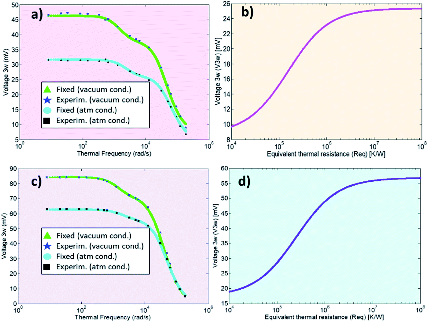 | ||
| Fig. 3 Calibration curves of the thermal response for two SThM probes from the same batch. In (a) and (c), the calibration curves in the vacuum and atmospheric conditions are plotted. In (b) and (d) are plotted the V3ωvs. Req, obtained with the heat transfer model. The curves in (a) and (b) corresponds to the first calibrated probe and (c) and (d) to the second calibrated probe. | ||
The calibration process was performed in two thermal probes using a different supply of voltage Vin in each one. In the first probe (Fig. 3a and 3b), a Vin of 4 Vpp was applied (Vrms of 2.8 V). As a result, the effective voltage measured after limiter resistance in the first probe was 1.17 V, and the current across the circuit was determined for one of the probe legs as 0.8 mA. In the second probe (Fig. 3c and 3d), a Vin of 6 Vpp was applied (Vrms of 4.24 V). After the limiter resistance in the second probe, the effective voltage was measured as 1.75 V, and the current was 1.2 mA. See ESI† for details of these values.
 | ||
| Fig. 4 In (a) the cross-point obtained with the first calibrated probe, supplied with a voltage of 2.8 V and a current of 0.8 mA. In (b) the cross-point obtained with the second probe, the supply voltage of 4.24 V, and the calculated current of 1.2 mA. Calibration samples used in each case are indicated for each graph. | ||
In our calibration procedure, a set of 10 samples with well-known thermal conductivity values were scanned and used as reference samples for two purposes. First, five samples, called calibration samples, were scanned to determine Rc and b with the cross-point method (SThM images in Fig. 5). Second, we used these parameters in the model to determine the thermal conductivity of another set of five samples, called test samples, to determine the accuracy of this method (SThM images in Fig. 6). The thermal conductivity results of the test samples were compared with the expected value of literature or cross-checked with other thermometry measurements. The set of calibration samples was composed of polycarbonate (κ = 0.20 W m−1 K−1), polyaniline with 5% graphene nano-platelets (PANI-5% GNP, κ = 0.49 W m−1 K−1), tellurium film (Te, κ = 0.77 W m−1 K−1), bismuth telluride film (Bi2Te3, κ = 0.97 W m−1 K−1), and borosilicate glass (κ = 1.1 W m−1 K−1). The set of test samples was composed of Kapton® polyimide film (Kapton, κ = 0.19 W m−1 K−1), high-density polyethylene (HDP, κ = 0.46 W m−1 K−1), PANI 7% GNP (κ = 0.65 W m−1 K−1), silicon germanium film (SiGe, κ = 1.2 W m−1 K−1) and machinable glass-ceramic (MACOR, κ = 1.5 W m−1 K−1). The thermal conductivity of polycarbonate, Kapton, HDP, and MACOR were reported from the literature and the manufacturer, while the thermal data of the samples of PANI 5% GNP, PANI 7% GNP, Te film, Bi2Te3 film, SiGe film, and borosilicate glass, were previously measured by photoacoustic (PA) and 3ω hot probe with Wollaston wire.27 The results of the test samples are in good agreement with the previously reported values (see Table 2).
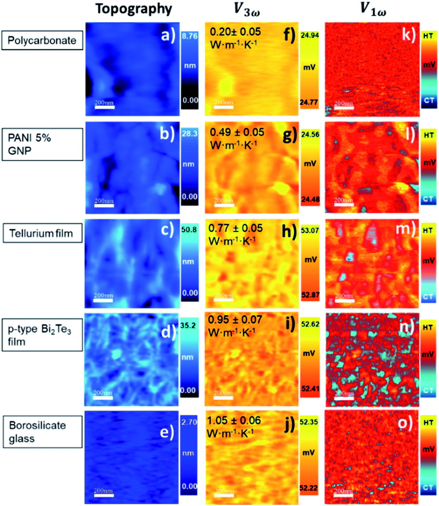 | ||
| Fig. 5 SThM images of the calibration samples. The topographic images are from (a) to (e). The corresponding voltage responses images: V3ω images are from (f) to (j), while V1ω images are from (k) to (o). The inset values in V3ω images are the thermal conductivity values fixed in the thermal model to obtain the cross-point curve. The scale bar is 200 nm in all the images. | ||
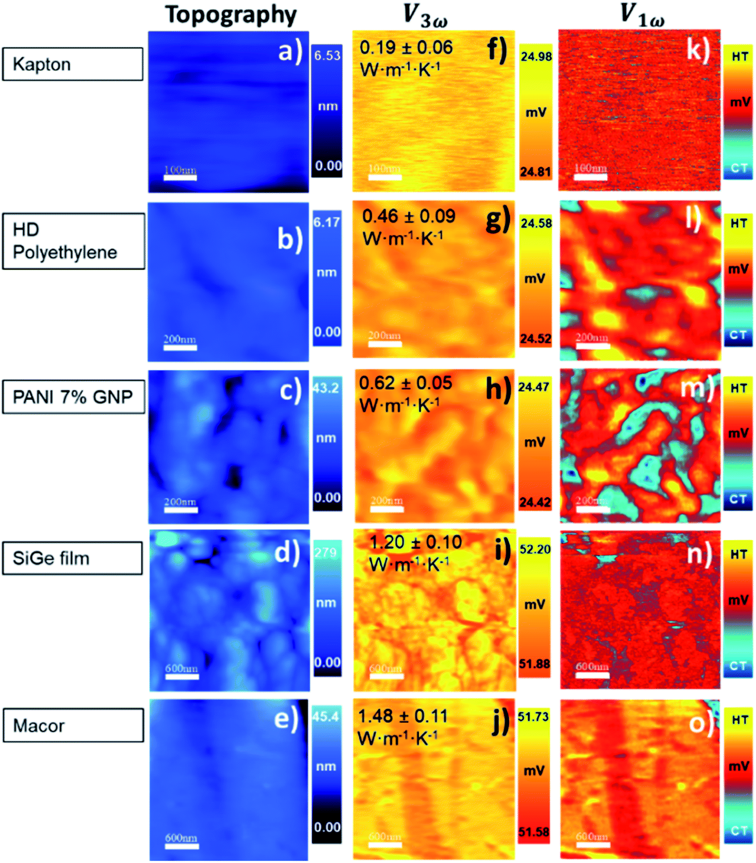 | ||
| Fig. 6 SThM images of the test samples. The topographic images are from (a) to (e). The images of voltage response: V3ω from (f) to (j), V1ω from (k) to (o). The inset thermal conductivity values were determined after measurements. The scale bar in each sample: Kapton images have 100 nm, HD polyethylene and PANI 7% GNP have 200 nm, SiGe and Macor have 600 nm. | ||
| References samples/expected thermal conductivity value κexp (W m−1 K−1) | Thickness (μm) | V 3ω × 10−3 (V) | R eq × 106 (K W−1) | b × 10−7 (m) | R c × 106 (K W−1) | R s × 106 (K W−1) | Thermal conductivity κs (W m−1 K−1) |
|---|---|---|---|---|---|---|---|
| *CAL1 calibration sample for cross-point of SThM probe 1, where Rc is (1.60 × 10⁶ ± 0.03) K W−1 and b is (3.85 × 10⁻⁷ ± 0.02) m. *CAL2 calibration sample for cross-point of SThM probe 2, where Rc is (0.94 × 10⁶ ± 0.02) K W−1 and b is (2.41 × 10⁻⁷ ± 0.02) m. | |||||||
| Kapton/(0.12–0.47) | Bulk | 24.86 | 5.02 | 3.85 | 1.60 | 3.42 | 0.19 ± 0.06 |
| Polycarbonate*CAL1/(0.19–0.22) | Bulk | 24.84*CAL1 | 4.85 | 3.85 | 1.60 | 3.25 | 0.20 ± 0.05 |
| High-density polyethylene/(0.45–0.52) | Bulk | 24.55 | 3.01 | 3.85 | 1.60 | 1.41 | 0.46 ± 0.09 |
| PANI 5% GNP*CAL1/(0.47–0.49) | Bulk | 24.53*CAL1 | 2.93 | 3.85 | 1.60 | 1.33 | 0.49 ± 0.05 |
| PANI 7% GNP/(0.65–0.68) | Bulk | 24.44 | 2.65 | 3.85 | 1.60 | 1.05 | 0.62 ± 0.05 |
| Tellurium film*CAL2/(κexp = 0.78–0.79) | 2.74 | 52.95*CAL2 | 2.29 | 2.41 | 0.94 | 1.35 | 0.77 ± 0.05 |
|
2.8 | 52.51*CAL2 | 2.03 | 2.41 | 0.94 | 1.09 | 0.95 ± 0.07 |
| Borosilicate glass*CAL1–CAL2/(1.08–1.10) | Bulk | 24.27*CAL1 | 2.19 | 3.85 | 1.60 | 0.59 | 1.10 ± 0.06 |
| 52.31*CAL2 | 1.93 | 2.41 | 0.94 | 0.98 | 1.05 ± 0.10 | ||
| SiGe film/(1.22–1.23) | 1.5 | 52.02 | 1.80 | 2.41 | 0.94 | 0.86 | 1.20 ± 0.10 |
| Macor/(1.40–1.50) | Bulk | 51.62 | 1.64 | 2.41 | 0.94 | 0.70 | 1.48 ± 0.11 |
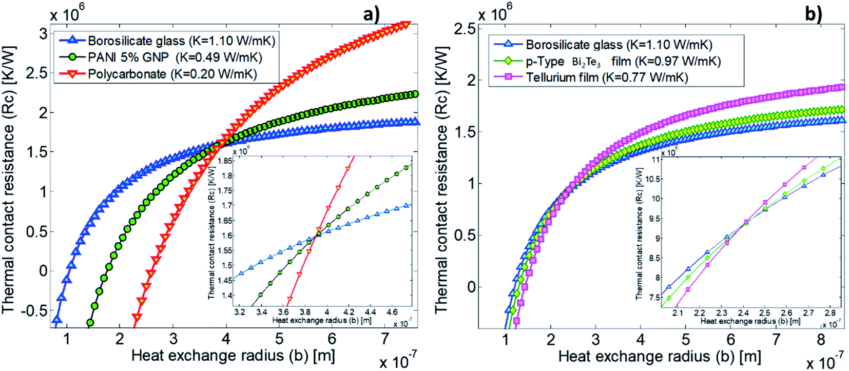
The cross point obtained for the first calibrated Pd/Si3N4 probe (feeding voltage Vrms = 2.8 V) is shown in Fig. 4a. The scanned calibration samples were polycarbonate, PANI 5% GNP, and borosilicate glass, with well-defined thermal conductivities of 0.20 W m−1 K−1, 0.49 W m−1 K−1, and 1.10 W m−1 K−1, respectively. These curves intersect at a value of 1.6 × 10⁶ K W−1 for Rc and 3.85 × 10⁻⁷ m for b. Fig. 4b shows the cross-point obtained for the second Pd/Si3N4 calibrated probe (feeding voltage Vrms = 4.24 V). The scanned calibration samples were Te film, Bi2Te3 film, and borosilicate glass, with well-known thermal conductivities of 0.77 W m−1 K−1, 0.97 W m−1 K−1, and 1.10 W m−1 K−1, respectively. The curves intersect at a value of 0.94 × 10⁶ K W−1 for Rc and 2.41 × 10⁻⁷ m for b. See these data in Table 2.
The topographic and thermal images obtained after scanning the calibration samples are shown in Fig. 5. The thermal images correspond to the V1ω and V3ω signals. They were acquired simultaneously with topographic images. The value inset in the V3ω thermal image is the known thermal conductivity fixed in the model. Topographic and thermal images of test samples are found in Fig. 6, and the inset value in V3ω thermal images is the measured value. The error is the deviation of the values when different thermal voltages in the images were analyzed. The dispersion of voltage values was less than one mV (see Section S.I.5†).
The samples were cleaned and/or polished before scanning with the thermal probe. The borosilicate glass was cleaned by applying acetone to a cotton swab. PANI and the films made of Te, Bi2Te3, and SiGe were polished using fine (1600) grit sandpaper, following the procedure in ref. 27. Some of these samples are commercial as polycarbonate, glass, and Kapton. The films were fabricated in our group. All the reference samples are bulk or film thick. For example, SiGe film has 1.5 μm of thickness. It was prepared by metal-induced crystallization sputtering and growth on a glass substrate. Te is a thick film with 2.74 μm of thickness and was produced by electrodeposition.
A first scan of the reference samples was done in the AFM with a silicon tip to explore the surface and ensure a smooth and cleaned area. Regarding the AFM scan parameters with the thermal probe, it is important to consider that the applied set point voltage should warrant a constant force probe to the sample. It has been reported that probe-sample applied force is highly dependent on the hardness properties,40 whether the material is metallic, ceramic, plastic, or composite. However, since exists a significant risk of crashing or losing the photodiode signal during the probe to sample approaching, this parameter should be selected with extreme care during the experiment. The setpoint was also chosen based on the roughness characteristics of each sample to prevent critical tip damage. Hence, a first approximation was made with the setpoint voltage values suggested by the AFM control unit. Then, when the approach was nearly completed, the probe withdrew and approached again to apply a similar set point in all the samples with similar hardness characteristics. As a result, the tip was approached and retracted several times before achieving the perfect alignment in probe-sample contact, meaning that no overpressure was applied to the samples. The selected setpoint varied between 0.07 V to 0.5 V. The ambient conditions in the laboratory during probe calibration and measurements of samples were: 25 °C, the temperature, and 30% relative humidity.
These results reflect some interesting conclusions. First, although the thermal exchange radius has varied between 100 nm and 400 nm, it should be emphasized that these values are much smaller than those obtained with a Wollaston wire using similar samples. The cross-point value obtained with the Wollaston probes in ref. 27 was around 0.45 × 10⁵ K W−1 for Rc and 2.8 × 10⁻⁶ m for b. Therefore, the intersected curves obtained with the hot probe method led to a higher heat exchange radius for the low thermal conductivity range, according to the tip's curvature radius in Wollaston probes (more than 2 μm). Using microfabricated probes, the heat exchange radius obtained with the cross-point method can be one order of magnitude lower than the one obtained for Wollaston probes. This can be expected for these types of probes. The second conclusion is that Rc increases by nearly two orders of magnitude relative to the Wollaston probe. The higher thermal contact resistance value of the Pd/Si3N4 probe compared with the Wollaston probe is consistent with the literature values. Values of Rc of 4.06 × 10⁶ K W−1 and 0.83 × 10⁶ K W−1 were reported by Puyoo et al.33 and Ge et al.,41 respectively, with microfabricated probes; while an Rc of 1.3 × 10⁵ K W−1 was reported by Thiery et al. with a Wollaston probe.42 A possible explanation for this difference could be related to the heat transfer process through solid–solid (Gss), water meniscus (Gw), and air surrounding (Gair) in the probe-sample interaction. Because the microfabricated probes have a sharper tip, the solid–solid contact area is smaller than the Wollaston probe, increasing the thermal contact resistance. This difference is linked to the probe itself and must be identified for each tip.
2.4. Thermal conductivity analysis of samples with unknown thermal conductivity
Once the calibration procedure is completed, we can use the 3ω-SThM technique to obtain the thermal measurements with confident results. The acquisition of high-resolution thermal images provides qualitative and quantitative information on sample thermal properties at the nanoscale level with quite an accuracy. One of the main advantages is that these measures can be done at atmospheric pressure with lab-made instrumentation. Due to the probe-sample configuration in the implemented technique, the measuring direction is perpendicular to the sample surface. Thus, we performed thermal conductivity measurements with our 3ω-SThM implemented technique out-of-plane from the sample surface. In crystalline materials, the direction of the growth plane could coincide with the direction of the measured plane, depending on the growth conditions of the sample. Therefore, anisotropic properties in the material may be considered. Consequently, the thermal conductivity is expected to be different in the in-plane direction than the value out-of-plane direction. Conversely, if the material is isotropic, the thermal conductivity parameter should be the same if measured parallel or perpendicular to the plane (independent of direction).Two scans were performed in each one of the samples, the first one at a velocity of 0.98 l per s (lines per second) to explore the thermal and topographic features. Then, a second scan with an optimized velocity was carried out to obtain the thermal information in the most satisfactory conditions, thus reducing the spike noise or artefacts during the scan. As a result, the scan velocity was elected between 0.2–0.98 l per s. We made at least three thermal scans in the same area to ensure data repeatability, and this process was repeated at different locations. This allowed detection of 1% to 5% variability in the thermal information depending on sample homogeneity and composition.
This implemented method allows us to obtain local map information on heat dissipation in different structures grown in our group by electrodeposition or sputtering technique. In this section, the unknown thermal conductivity of different samples (that can be assumed to have bulk-like thickness) is determined using eqn (3) under the semi-infinite medium assumption. In samples with two or more materials, it is necessary to apply the effective medium theory to identify individual material properties.43 One example is composite materials, e.g., porous structures or nanowires embedded in a matrix.2,24,44 In that case, we will provide an effective thermal conductivity value, as shown in Table 3 (see ESI† for more details).
| Samples with unknown thermal conductivity value κexpected (W m−1 K−1) | Thickness λ (μm) | V 3ω × 10−3 (V) | R eq × 106 (K W−1) | b × 10−7 (m) | R c × 106 (K W−1) | R s × 106 (K W−1) | Thermal conductivity κs (W m−1 K−1) |
|---|---|---|---|---|---|---|---|
| a *C1/C2 first-row cross-point 1 and second-row cross-point 2; κc is the composite thermal conductivity. In these cases, the κs (the first value) is the thermal conductivity obtained after applying the effective medium theory. | |||||||
| Si0.8Ge0.2 nanomeshed porous ∅p = 20 nm/(0.55 ± 0.10)*C1/C2 | ∼0.5 | 24.48 | 2.77 | 3.85 | 1.60 | 1.17 | 0.57 ± 0.15 |
| κ c = 0.55 ± 0.11 | |||||||
| 53.59 | 2.79 | 2.41 | 0.94 | 1.85 | 0.58 ± 0.12 | ||
| κ c = 0.56 ± 0.08 | |||||||
| Si0.8Ge0.2 nanomeshed porous ∅p = 137 nm/(0.93 ± 0.15)*C1/C2 | ∼0.5 | 24.33 | 2.35 | 3.85 | 1.60 | 0.75 | 0.91 ± 0.16 |
| κ c = 0.87 ± 0.13 | |||||||
| 52.60 | 2.08 | 2.41 | 0.94 | 1.13 | 0.95 ± 0.13 | ||
| κ c = 0.91 ± 0.10 | |||||||
| Si0.8Ge0.2 nanomeshed porous ∅p = 294 nm/(1.54 ± 0.27)*C1/C2 | ∼0.5 | 24.35 | 2.40 | 3.85 | 1.60 | 0.79 | 1.15 ± 0.18 |
| κ c = 0.81 ± 0.16 | |||||||
| 52.43 | 1.99 | 2.41 | 0.94 | 1.05 | 1.40 ± 0.13 | ||
| κ c = 0.99 ± 0.10 | |||||||
| AAO 24 nm*C2/(1.04 ± 1.36) | 53 | 52.18 | 1.87 | 2.41 | 0.94 | 0.92 | 1.29 ± 0.10 |
| κ c = 1.12 ± 0.07 | |||||||
| Ag2Se*C2/(0.64 ± 0.10) | 0.95 | 53.36 | 2.59 | 2.41 | 0.94 | 1.64 | 0.63 ± 0.07 |
| Ag2−xSe*C2/(0.5–1.5) | 0.95 | 53.17 | 2.44 | 2.41 | 0.94 | 1.50 | 0.69 ± 0.15 |
| Cu2Se (smooth)*C2/(0.80 ± 0.10) | 0.85 | 52.89 | 2.25 | 2.41 | 0.94 | 1.31 | 0.79 ± 0.03 |
| Cu2Se (rough)*C2/(0.80 ± 0.10) | 0.85 | 52.82 | 2.21 | 2.41 | 0.94 | 1.27 | 0.82 ± 0.04 |
|
∼2 | 52.56 | 2.06 | 2.41 | 0.94 | 1.12 | 0.93 ± 0.12 |
We determine the thermal conductivity of different thermoelectric films. These samples exhibit variations such as porous structure, material compositional changes, the effect of roughness and smooth of the surfaces, grain size reduction, and the different grain shape. First, we present the measurements of the alloy silicon–germanium Si0.8Ge0.2 nano-meshed. In these films, the effect of porous structure on thermal conductivity was studied. In addition, we measure chalcogenide materials films: silver selenide (Ag2Se), copper selenide (Cu2Se), and bismuth telluride (Bi2Te3). We study the thermal conductivity changes associated with phase transition changes in the case of Ag2Se films, the roughness influence in Cu2Se (in a free-standing film), and the grain size and crystalline size reduction in a film with a branch structure of Bi2Te3. These sample features were carefully chosen to compare how the morphological and compositional differences can affect their thermal properties. The aim is to prove the power of this implemented technique by measuring fabricated samples in our group with the best thermoelectric properties and different characteristics between them. These results can contribute to understanding the heat transport mechanism in materials structured at micro and nanoscales. Also, this technique can offer very high-resolution images for local determination of impurities, conductivity changes, or sample damages at these scales.
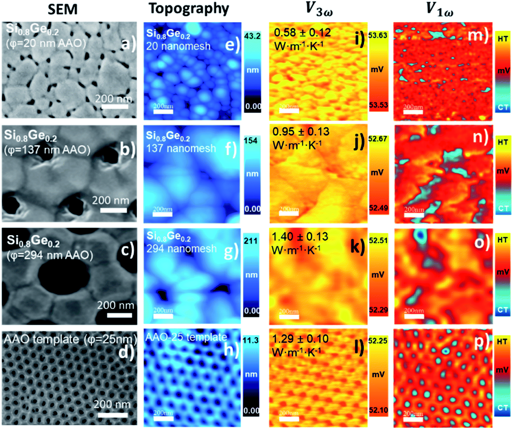 | ||
| Fig. 7 Images of the nano-porous structures of Si0.8Ge0.2 films in the first three rows and one template of AAO in the last row. SEM micrographs from (a) to (d). Topographic images from (e) to (h). The inset numbers in these images are the pore diameter value obtained through SEM images. Thermal images with the voltage response of V3ω from (i) to (l) and from (m) to (p) the voltage response of V1ω. The thermal conductivity values obtained with this SThM technique are inset in the images of V3ω. The scale bar in all the images corresponds to 200 nm. | ||
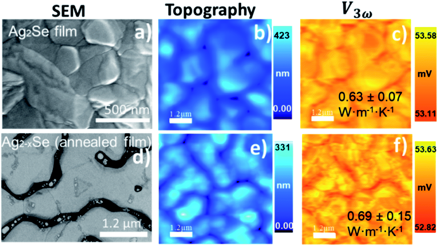 | ||
| Fig. 8 Ag2Se before annealing in the first row (a to c) and images of the same film after heating at 437 K in the second row (d to f). The scale bar (white line) in SEM micrograph in (a) has 500 nm. The scale bar in SEM micrograph in (d), topographic images in (b) and (e), and V3ω thermal images in (c) and (f), represent 1.2 μm. | ||
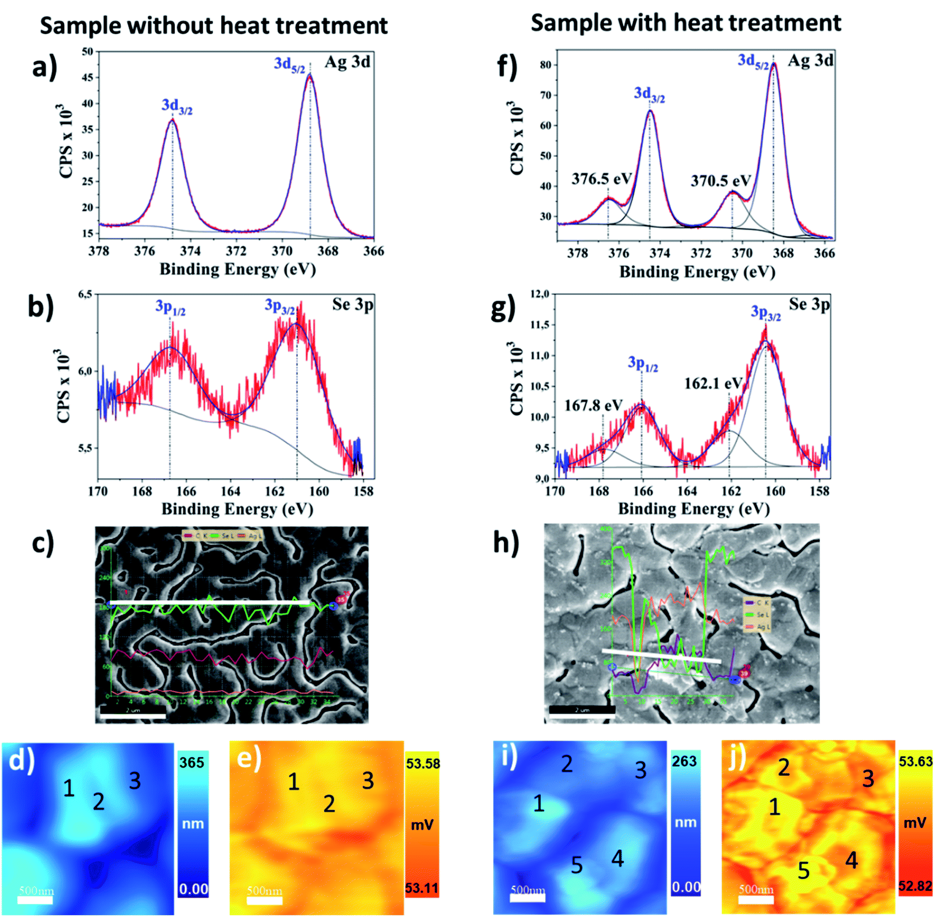 | ||
| Fig. 9 Measurements in the silver selenide films, the sample without heat treatment (left-hand side) and the sample with heat treatment (right-hand side), with analysis of XPS (a, b, f and g), EDX (c and h), and SThM (d, e, i and j). High-resolution room temperature XPS spectra for stoichiometric Ag2Se film are obtained for Ag 3d in (a) and Se 3p in (b), and after sample annealed in (f) and (g), respectively. In (c) EDX micrograph of the sample without heat treatment shows that the content of Ag/Se has no significant variations along with the line profile (white line). In (h), the heated sample presents silver-rich clusters along with the EDX line profile. The topographic images are shown in (d) and (i), and the V3ω thermal images are found in (e) and (j). The inset numbers in SThM images correspond to a local analysis in different sample regions. | ||
Specifically, for the silver selenide films, further studies were conducted to investigate the possible segregation of the Ag after the heating processes. The high-resolution XPS spectra show one binding energy (BE) with the peak Ag 3d5/2 = 368.8 ± 0.2 eV (Fig. 9a) typical of Ag alloys atomically bonded to Se with the peak Se 3p3/2 = 160.7 eV ± 0.2 eV (Fig. 9b). After a heating process in this film (at 437 K), the annealed Ag2−xSe film presented additional peaks, the Ag 3d5/2 = 370.5 eV (Fig. 9f) and the Se 3p3/2 = 162.1 eV (Fig. 9g), which can be associated with a process of material segregation due to the heating. EDX micrograph in Fig. 9c has no difference in Ag/Se content since the Ag (green curve) and Se (orange curve) are constant along with the line profile (white line). However, the EDX micrograph of the heated sample shows material segregation that is silver-rich. In Fig. 9h, the line profile analysis of a silver-rich cluster has the Ag content increased when Se decreased. The inset numbers in the SThM images of Fig. 9 represent different regions that were locally analyzed. In the topographic image (Fig. 9d) of the analyzed regions (1), (2), and (3) for the sample without annealing, a slight height difference is observed. Nevertheless, homogenous voltage distribution in the 3ω image (Fig. 9e) is obtained. In this case, the average value of thermal conductivity was 0.63 ± 0.02 W m−1 K−1. The thermally treated film was locally analyzed in regions (1), (2), (3), (4), and (5), with differences in the topography (Fig. 9i) and in the 3ω voltage (Fig. 9j). The thermal conductivity results in each region are: 0.58 ± 0.04 W m−1 K−1 (1), 0.64 ± 0.06 W m−1 K−1 (2), 0.72 ± 0.03 W m−1 K−1 (3), 0.71 ± 0.06 W m−1 K−1 (4), and 0.55 ± 0.06 W m−1 K−1 (5). The thermal conductivity analysis shows differences that can be related to the silver segregation observed by XPS and EDX analysis (see discussion of these results in Section 2.5).
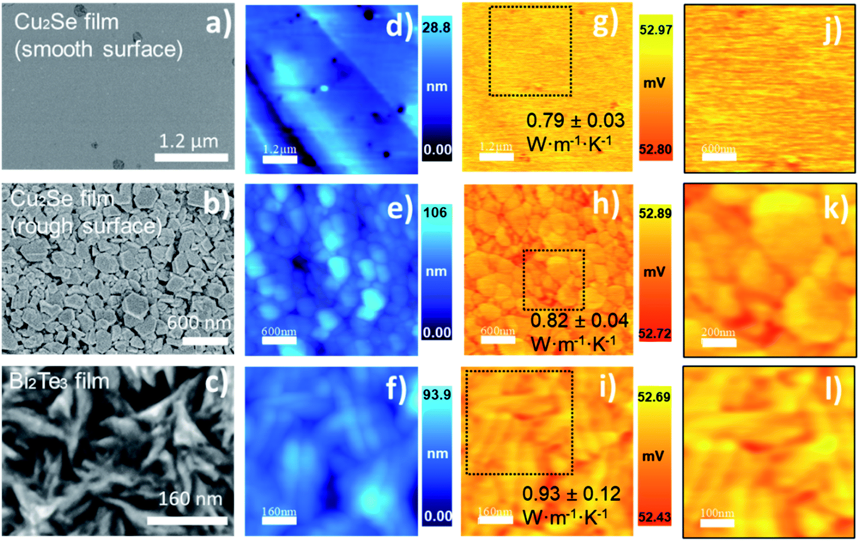 | ||
| Fig. 10 Cu2Se, and Bi2Te3 thermoelectric films. SEM micrographs from (a) to (c) and the topographical images from d) to f). The SThM thermal images V3ω from (g) to (i) with their respective zoomed regions from (j) to (l). The topographical and thermal images have a scale bar of 1.2 μm, 600 nm and 160 nm, for Cu2Se, Cu2Se rough surface and Bi2Te3 film, respectively. | ||
Finally, to prove the high resolution of our implemented technique, we studied the effect of grain size reduction in Bi2Te3 material. Currently, this is one of the most important thermoelectric materials. The images in the last row of Fig. 10, correspond to Bi2Te3 thermoelectric film grown by electrodeposition.46 It is observable the branching structure of this sample by SEM micrograph (Fig. 10c), topography image (Fig. 10f), and thermal images (Fig. 10i and l). Although some changes are observed in V3ω, these can be attributed to the geometric features (interconnected branches). However, regardless of the topographical features, the analysis of the thermal images gives, on average, a uniform distribution of the thermal conductivity, given the slight variation of the thermal image.
2.5. Validation and discussion of measurements in thermoelectric films
We measured the nanostructures of Si0.8Ge0.2 which are nano-meshed films obtained by replication of the nano-porous structure from anodic aluminum oxide (AAO) membranes. The interest in this type of structure lies in the potential to increase their TE efficiency. However, they represent a challenge from the characterization point of view because air confinement effects or substrate contribution can affect the thermal measurements. After the measurements, we can highlight, on the one hand, that decreasing the porous size allows for a decrease the thermal conductivity. Here, the porous and grain boundaries play an essential role in the phonon scattering to decrease the thermal conductivity. On the other hand, as was observed in the most significant porous size, the microfabricated probe could lose physical contact with the sample surface. Therefore, it should be carefully analyzed in future measures to obtain more reliable results, such as a combination of contact and non-contact thermal models. We apply the effective medium theory (see S.I.5†) and corroborate the results with previously reported values in ref. 16. In this case, we obtained a deviation up to 14% in the thermal conductivity of the film with a porous size of 294 nm. The films with porous of 19 nm and 137 nm have a thermal conductivity quite in agreement with reported values.16Other relevant thermoelectric materials are the chalcogenides family. We study the transport properties of nanostructured samples of silver selenide, copper selenide and bismuth telluride. The obtained thermal conductivity values for these chalcogenides' materials are compared with the reported values in the literature, measured along the c-axis, and perpendicular to this. These results are discussed in this section. We used the Wiedemann–Franz (WF) law to determine roughly the impact of the electronic contribution (κe) to the total measured thermal conductivity in this set of samples. We estimate a lattice thermal conductivity of ∼0.22 W m−1 K−1 and ∼0.13 W m−1 K−1 for Ag2Se and Ag2−xSe, respectively, and of ∼0.2 W m−1 K−1 for the Cu2Se films. Finally, we estimated a phonon contribution to the thermal conductivity of 0.62 W m−1 K−1 for the bismuth telluride samples.
Regarding the selenide samples, it is important to consider that they present ionic conduction, i.e., copper or silver ions moving in the selenium like in a liquid.47 This means that thermal conductivity can be decreased by the scattering mechanism at the time that electrical conductivity is transported by ions. This can be understood as the increment of phonon scattering due to nano-structuration effects that cause a reduction in the thermal conductivity because the lattice thermal conductivity (κl) is reduced, and therefore, the total thermal conductivity in films is reduced too (κ = κl + κe).
The silver selenide, Ag2Se, n-type semiconductor, has reached a thermoelectric efficiency near one (zT ∼ 1) at room temperature.48 This opens the possibility for this semiconductor to be implemented in different TE devices, operating at low temperatures. Ag2Se exhibits superionic conduction at the phase transition temperature. Upper this critical temperature (∼406 K), the Ag2Se is reordered in a cubic phase. The thermal transport will vary around this temperature due to changes in the electronic conduction, as well as changes in the electrical conduction due to a metallic performance in the sample. The thermal conductivity in the Ag2Se bulk sample was reported to be double the value at room temperature in the phase transition temperature; it varied from 1.5 W m−1 K−1 to 3 W m−1 K−1, respectively.48 The value of 1.2 W m−1 K−1 for the Ag2Se in bulk has been recently reported in ref. 49. These values reported for this bulk material are near one order of magnitude higher than the reported for silver selenide in nanostructures by Ding Y. et al. in 2019, of 0.48 W m−1 K−1, ref. 50. Perez-Taborda J. A., et al., reported a value for Ag2Se thin films of 0.64 W m−1 K−1 at room temperature in pulsed hybrid reactive magnetron sputtering (PHRMS).30 As the critical temperature can be easily reached during the fabrication process or in the material implementation, it must be studied the thermal conductivity performance in Ag2Se nanostructures at room temperature and when these samples are close to this phase transition temperature. Therefore, this analysis was made before and after annealing the Ag2Se sample at 437 K.
The thermal results in silver selenide samples can be correlated with compositional features in the material through XPS and EDX measurements. In Fig. 9a and b, the high XPS resolution at room temperature of the measured Ag2Se sample shows only one binding energy (BE) for Ag 3d5/2 and Se 3p3/2 in Ag 3d and Se 3p, respectively. This means that there is only an oxidation state for the Ag and Se, which is compatible with Ag2Se stoichiometry (with an oxidation state of Ag1+ and Se2−) as detected by XRD. The Ag 3d5/2 = 368.8 ± 0.2 eV is typical of Ag1+.51 The binding energy Se 3p3/2 = 160.7 ± 0.2 eV shows a Se–Ag interaction type with selenium oxidation states between Se2− and Se0 (binding energy of Se2− < Se0), which is in agreement with the literature reports.51–53 After the heat treatment up to temperatures of 437 K, the high XPS resolution at room temperature shows additional peaks with BE of Ag 3d5/2 in 368.5 eV and 370.5 eV. The Ag 3d5/2 = 368.5 eV has a higher BE than in the case of the pure metal, indicating the formation of another Ag compound different from the previous one, Fig. 9f. Similarly, it can be observed in Fig. 9g, the BE of Se 3p shows two peaks for Se 3p3/2 at 160.4 eV and 162.1 eV, which represents two types of selenium in the sample, different from the selenium before heating. This XPS measurement indicates that the initial Ag2Se films are divided into two phases, one Ag2−xSe and a new silver-rich phase in which some selenium is still present, indicating that the clusters are not only silver but a silver selenide very silver-rich.
In this work, our reported values for Ag2Se films grown by PHRMS lie within the range of 0.63 W m−1 K−1 to 0.69 W m−1 K−1. These results indicate that thermal conductivity has risen in the case of the sample with annealing treatment. It was probably due to the silver-rich clusters detected by SEM-EDX and the compositional changes analyzed with XPS. We also simulated the heat transport in a silver selenide film with COMSOL Multiphysics. These simulation values were consistent with the experimentally measured thermal conductivities for the corresponding silver selenides samples without heat treatment (see S.I.6†). However, further analysis should be addressed to understand why some regions exhibit a low thermal conductivity value, as in the case of region number 5 in Fig. 9j.
Copper selenide, Cu2Se, a p-type semiconductor, exhibits superionic conduction at the phase transition temperature (∼410 K) and a zT = 1.8 at 973.15 K has been reported.54 However, at high temperatures, some stability problems in its ionic conduction had been reported.55 Therefore, we are interested in his performance around room temperature. We are studying the effect that a roughness surface can add to the thermal conductivity measurements in a free-standing sample. This analysis aims to elucidate if this factor can be significant to the thermal measurements or if, on the contrary, this parameter can be neglected in these measurements. Thermal conductivity values for bulk Cu2Se as high as 2.7 W m−1 K−1 have been reported in ref. 56. However, the value determined for bulk Cu2Se reported by Liu et al. achieved the lowest value of 1 W m−1 K−1 in ref. 47. These values in bulk samples have been reduced with nano-structuration. Gahtori, B., et al. in ref. 56, reported thermal conductivity of 0.75 W m−1 K−1 in nano Cu2Se. And the films of copper selenide growth by PHRMS in a work published by Perez-Taborda J. A., et al.,45 showed a reduction of thermal conductivity to 0.80 W m−1 K−1. Although the samples measured in our experiment were grown by PHRMS,45 in this case, we are measuring a sample that was prepared as a free-standing film, allowing us to measure both sides of the same sample to compare the results. In our experiment, the free-standing Cu2Se film, has thermal conductivities values of 0.79 W m−1 K−1 and 0.82 W m−1 K−1 for the smoothed and the rough surface, respectively. These values are between the error of the technique and are in good agreement with the ones published.45,56
In the case of n-type bismuth telluride, Bi2Te3, the values are spread in a range between 3.3 W m−1 K−1 to 0.34 W m−1 K−1, depending on whether it is bulk,57,58 or thin films.46,59–61 Since this is an anisotropic material, our experimental measurement of thermal conductivity in Bi2Te3 was obtained perpendicular to the c-axis; this film was highly oriented in the [1 1 0] direction (see S.I.8†). Comparing only the values obtained for films, one can observe that thermal conductivity perpendicular to the c-axis is expected to be higher than the thermal conductivity value determined along the c-axis. This can be understood through the strong covalent bonds that are present perpendicular to the c-axis.2,46 The contribution of the boundaries to the phonon scattering has been reported to reduce the thermal conductivity as in ref. 60. Therefore, the increase of grain boundaries and reduction of crystallite size and grain size causes a reduction in the thermal conductivity value, reaching an average value of 0.93 W m−1 K−1 in this work.
2.6. Final remarks
The discussion of these data can be extended to analyze different samples with similar transport properties and within a low thermal conductivity range (<3 W K−1 m−1). Other characteristics of the sample's material can vary. They can be insulators or semiconductors, amorphous or crystalline, but desirably, as flat as possible to avoid tip damage during the scan. The measurement results presented in this work are a good indicator that, by analyzing samples with a similar value of thermal conductivity (in the range of low values), it is possible to determine this physical sample property with high accuracy and high resolution, using multiple data points and thermal mapping.Generally, experimental thermal characterization techniques at the microscale face different challenges (e.g. need for a transducer in optical measurements, limited spatial resolution, etc.). However, many of these issues can be overcome with the SThM technique, which can determine almost instantaneously—after proper calibration and standardization of the measurements-the thermal performance of a material in a device configuration or microchip. Furthermore, this method offers the possibility to scan many locations in the sample surface with scan areas about 10 μm2 to 0.1 cm2 (100 nm × 100 nm or 10 μm × 10 μm), and with scan pixels of 256 × 256 or 512 × 512 points. This increases the statistical data points for the analysis, allowing to improve the accuracy of the calculations. The field of application of this technique is wide because one of the main characteristics is that the thermal conductivity can be obtained directly from the measurements and not by indirect measures, for example, through thermal diffusivity. This technique can be used to determine the thermal information by quantitative analysis and allows for the acquisition of valuable qualitative information through the thermal maps. These thermal maps offer information on the heat dissipation on the surface, observing its homogeneities and heterogeneities. For example, it could significantly impact the thermal analysis of semiconductor–insulator-based flexible films and devices for TE applications62 and the thermal conductivity analysis in organic/inorganic hybrid film transistors and sensors.63 Also, to assess the hot spots in photovoltaic–thermoelectric coupling devices with thermal interface materials64 or to evaluate the heat dissipation in microchips for coolers microdevices.65 Or, as another relevant example, the SThM technique has contributed recently to sense for the first time the temperature of hot spots produced by filaments in resistive random access memory devices (RRAM), a long-lasting challenge for electrical engineering community,66 to cite some.
3. Conclusions
In this work, we have determined the thermal contact resistance and the thermal exchange radius of the Pd/Si3N4 probes using the 3ω-SThM method and the cross-point calibration method. This calibration was performed in the low thermal conductivity range (between 0.19 ± 0.06 and 1.48 ± 0.11 W m−1 K−1). This method resulted in values of Rc = (0.94 × 10⁶ ± 0.02) K W−1 and b = (2.41 × 10⁻⁷ ± 0.02) m. The SThM probes show a significant improvement in these thermal parameters compared to other contemporaneous probes, like Wollaston probes, which using similar calibration samples obtained a thermal contact resistance Rc = 0.45 × 10⁵ K W−1 and the spatial resolution b = 2.8 × 10⁻⁶ m. During calibration, we highlighted the importance of considering stable electrical circuit connections, heat transfer mechanisms in the tip–probe interaction, software input data with known and unknown parameters, and measuring parameters to enable optimal data acquisition of the 1ω and 3ω signals. We confirmed that this method could be used for thermal analysis at the nanoscale by successfully determining the thermal conductivity of previously measured samples. As a result of our experimental setup, a high signal-to-noise ratio overcomes the issues of sensitivity to slight thermal conductivity variations and improves the thermal contrast images.We took advantage of the calibrated SThM probes to determine the thermal conductivity of Ag2Se, Ag2−xSe, Cu2Se (smooth surface), Cu2Se (rough surface), and Bi2Te3, which resulted in thermal conductivities—in units of W m−1 K−1, with values of 0.63 ± 0.07, 0.69 ± 0.15, 0.79 ± 0.03, 0.82 ± 0.04, and 0.93 ± 0.12, respectively. Beyond this, high-resolution thermal maps can also show thermal heterogeneities at the nanoscale. As an example, the thermal map of Ag2−xSe showed regions with different thermal properties allowing us to correlate it with different material phases. Overall, we can conclude that we have successfully calibrated Pd/Si3N4 probes to obtain thermal data from the 3ω-SThM signals, thus providing a way for quantitative analysis with nanoscale resolution.
Conflicts of interest
There are no conflicts to declare.Acknowledgements
We want to acknowledge the MINECO project PID2020-118430GB-100 for financial support. The authors acknowledge also the service from SEM for the MiNa Laboratory at IMN, and their funding CM (project SpaceTec, S2013/ICE2822), MINECO (Project CSIC13-4E-1794), and EU (FEDER, FSE).References
- J. Lu, T. Wu and K. Amine, Nat. Energy, 2017, 2, 1–13 CrossRef.
- M. M. Rojo, B. Abad, C. V. Manzano, P. Torres, X. Cartoixà, F. Alvarez and M. M. Gonzalez, Nanoscale, 2017, 9, 6741–6747 RSC.
- E. de Lucas-Gil, J. n. J. Reinosa, K. Neuhaus, L. Vera-Londono, M. Martín-González, J. F. Fernández and F. Rubio-Marcos, ACS Appl. Mater. Interfaces, 2017, 9, 26219–26225 CrossRef CAS PubMed.
- P. M. Resende, R. Sanz, O. Caballero-Calero and M. Martín-González, Adv. Opt. Mater., 2018, 6, 1800408 CrossRef.
- A. Ruiz-Clavijo, S. Ruiz-Gomez, O. Caballero-Calero, L. Perez and M. Martin-Gonzalez, Phys. Status Solidi RRL, 2019, 1900263 CrossRef CAS.
- T. Swoboda, K. Klinar, A. S. Yalamarthy, A. Kitanovski and M. Muñoz Rojo, Adv. Electron. Mater., 2020, 2000625 Search PubMed.
- Y. Xiang, X. Li, Y. Cheng, X. Sun and Y. Yang, Mater. Today, 2020, 36, 139–157 CrossRef CAS.
- J. Nan, X. Guo, J. Xiao, X. Li, W. Chen, W. Wu, H. Liu, Y. Wang, M. Wu and G. Wang, Small, 2019, 1902085 Search PubMed.
- A. E. Ostfeld, A. M. Gaikwad, Y. Khan and A. C. Arias, Sci. Rep., 2016, 6, 26122 CrossRef CAS PubMed.
- D. Beretta, N. Neophytou, J. M. Hodges, M. G. Kanatzidis, D. Narducci, M. Martin-Gonzalez, M. Beekman, B. Balke, G. Cerretti and W. Tremel, Mater. Sci. Eng., R, 2019, 138, 100501 CrossRef.
- Q. Shi, B. Dong, T. He, Z. Sun, J. Zhu, Z. Zhang and C. Lee, InfoMat, 2020, 2, 1131–1162 CrossRef.
- A. A. Balandin, Nat. Mater., 2011, 10, 569–581 CrossRef CAS PubMed.
- M. Bacon, S. J. Bradley and T. Nann, Part. Part. Syst. Charact., 2014, 31, 415–428 CrossRef CAS.
- M. Rull-Bravo, A. Moure, J. Fernandez and M. Martín-González, RSC Adv., 2015, 5, 41653–41667 RSC.
- J.-K. Yu, S. Mitrovic, D. Tham, J. Varghese and J. R. Heath, Nat. Nanotechnol., 2010, 5, 718–721 CrossRef CAS PubMed.
- J. A. Perez-Taborda, M. M. Rojo, J. Maiz, N. Neophytou and M. Martin-Gonzalez, Sci. Rep., 2016, 6, 32778 CrossRef CAS PubMed.
- P. Liu, Z. Fan, A. Mikhalchan, T. Q. Tran, D. Jewell, H. M. Duong and A. M. Marconnet, ACS Appl. Mater. Interfaces, 2016, 8, 17461–17471 CrossRef CAS PubMed.
- R. Wang, T. Wang, H. Zobeiri, P. Yuan, C. Deng, Y. Yue, S. Xu and X. Wang, Nanoscale, 2018, 10, 23087–23102 RSC.
- M. Ruoho, K. Valset, T. Finstad and I. Tittonen, Nanotechnology, 2015, 26, 195706 CrossRef PubMed.
- J. Liu, J. Zhu, M. Tian, X. Gu, A. Schmidt and R. Yang, Rev. Sci. Instrum., 2013, 84, 034902 CrossRef PubMed.
- A. Majumdar, J. Carrejo and J. Lai, Appl. Phys. Lett., 1993, 62, 2501–2503 CrossRef CAS.
- L. Vera-Londono, O. Caballero-Calero, J. A. Pérez-Taborda and M. Martín-González, in Coatings and Thin-Film Technologies, IntechOpen, 2018 Search PubMed.
- Y. Zhang, W. Zhu, F. Hui, M. Lanza, T. Borca-Tasciuc and M. Muñoz Rojo, Adv. Funct. Mater., 2020, 30, 1900892 CrossRef CAS.
- L. Vera-Londono, A. Ruiz-Clavijo, O. Caballero-Calero and M. Martín-González, Nanoscale Adv., 2020, 2, 4591 RSC.
- E. Puyoo, S. Grauby, J.-M. Rampnoux, E. Rouvière and S. Dilhaire, Rev. Sci. Instrum., 2010, 81, 073701 CrossRef PubMed.
- T. Borca-Tasciuc, Annu. Rev. Heat Transfer, 2013, 16, 211–258 CrossRef.
- A. A. Wilson, M. M. Rojo, B. Abad, J. A. Perez, J. Maiz, J. Schomacker, M. Martín-Gonzalez, D.-A. Borca-Tasciuc and T. Borca-Tasciuc, Nanoscale, 2015, 7, 15404–15412 RSC.
- R. J. Pylkki, P. J. Moyer and P. E. West, Jpn. J. Appl. Phys., 1994, 33, 3785 CrossRef CAS.
- I. Horcas, R. Fernández, J. Gomez-Rodriguez, J. Colchero, J. Gómez-Herrero and A. Baro, Rev. Sci. Instrum., 2007, 78, 013705 CrossRef CAS PubMed.
- J. A. Perez-Taborda, O. Caballero-Calero, L. Vera-Londono, F. Briones and M. Martin-Gonzalez, Adv. Energy Mater., 2018, 8, 1702024 CrossRef.
- D. G. Cahill, Rev. Sci. Instrum., 1990, 61, 802–808 CrossRef CAS.
- S. Lefèvre and S. Volz, Rev. Sci. Instrum., 2005, 76, 033701 CrossRef.
- E. Puyoo, S. Grauby, J.-M. Rampnoux, E. Rouvière and S. Dilhaire, J. Appl. Phys., 2011, 109, 024302 CrossRef.
- Y. Zhang, C. L. Hapenciuc, E. E. Castillo, T. Borca-Tasciuc, R. J. Mehta, C. Karthik and G. Ramanath, Appl. Phys. Lett., 2010, 96, 062107 CrossRef.
- L. Thiery, E. Gavignet and B. Cretin, Rev. Sci. Instrum., 2009, 80, 034901 CrossRef PubMed.
- A. A. Wilson, PhD thesis, Analysis of non-contact and contact probe-to-sample thermal exchange for quantitative measurements of thin film and nanostructure thermal conductivity by the scanning hot probe method, Rensselaer Polytechnic Institute, 2017.
- S. Gomès, A. Assy and P. O. Chapuis, Phys. Status Solidi A, 2015, 212, 477–494 CrossRef.
- P. Tovee, M. Pumarol, D. Zeze, K. Kjoller and O. Kolosov, J. Appl. Phys., 2012, 112, 114317 CrossRef.
- J. Spiece, C. Evangeli, K. Lulla, A. Robson, B. Robinson and O. Kolosov, J. Appl. Phys., 2018, 124, 015101 CrossRef.
- Y. Li, N. Mehra, T. Ji and J. Zhu, Nanoscale Horiz., 2018, 3, 505–516 RSC.
- Y. Ge, Y. Zhang, J. A. Booth, J. M. R. Weaver and P. S. Dobson, Nanotechnology, 2016, 27, 1–14 CrossRef PubMed.
- L. Thiery, S. Toullier, D. Teyssieux and D. Briand, J. Heat Transfer, 2008, 130, 091601 CrossRef.
- A. I. Persson, Y. K. Koh, D. G. Cahill, L. Samuelson and H. Linke, Nano Lett., 2009, 9, 4484–4488 CrossRef CAS PubMed.
- M. M. Rojo, J. Martín, S. Grauby, T. Borca-Tasciuc, S. Dilhaire and M. Martin-Gonzalez, Nanoscale, 2014, 6, 7858–7865 RSC.
- J. A. Perez-Taborda, L. Vera, O. Caballero-Calero, E. O. Lopez, J. J. Romero, D. G. Stroppa, F. Briones and M. Martin-Gonzalez, Adv. Mater. Technol., 2017, 2, 1700012 CrossRef.
- C. V. Manzano, B. Abad, M. M. Rojo, Y. R. Koh, S. L. Hodson, A. M. L. Martinez, X. Xu, A. Shakouri, T. D. Sands and T. Borca-Tasciuc, Sci. Rep., 2016, 6, 19129 CrossRef CAS PubMed.
- H. Liu, X. Shi, F. Xu, L. Zhang, W. Zhang, L. Chen, Q. Li, C. Uher, T. Day and G. J. Snyder, Nat. Mater., 2012, 11, 422–425 CrossRef CAS PubMed.
- T. Day, F. Drymiotis, T. Zhang, D. Rhodes, X. Shi, L. Chen and G. J. Snyder, J. Mater. Chem. C, 2013, 1, 7568–7573 RSC.
- P. Jood, R. Chetty and M. Ohta, J. Mater. Chem. A, 2020, 8, 13024–13037 RSC.
- Y. Ding, Y. Qiu, K. Cai, Q. Yao, S. Chen, L. Chen and J. He, Nat. Commun., 2019, 10, 1–7 CrossRef PubMed.
- J. Chastain and R. C. King Jr, Handbook of X-ray photoelectron spectroscopy, Perkin-Elmer Corporation, 1992, vol. 40, p. 221 Search PubMed.
- N. Shevchik, M. Cardona and J. Tejeda, Phys. Rev. B: Solid State, 1973, 8, 2833 CrossRef CAS.
- S. Zembutsu, Appl. Phys. Lett., 1981, 39, 969–971 CrossRef CAS.
- L.-l. Zhao, X.-l. Wang, J.-y. Wang, Z.-x. Cheng, S.-x. Dou, J. Wang and L.-q. Liu, Sci. Rep., 2015, 5, 1–6 Search PubMed.
- G. Dennler, R. Chmielowski, S. Jacob, F. Capet, P. Roussel, S. Zastrow, K. Nielsch, I. Opahle and G. K. Madsen, Adv. Energy Mater., 2014, 4, 1301581 CrossRef.
- B. Gahtori, S. Bathula, K. Tyagi, M. Jayasimhadri, A. Srivastava, S. Singh, R. Budhani and A. Dhar, Nano Energy, 2015, 13, 36–46 CrossRef CAS.
- H. Goldsmid, Proc. Phys. Soc. B, 1956, 69, 203 CrossRef.
- J. Fleurial, L. Gailliard, R. Triboulet, H. Scherrer and S. Scherrer, J. Phys. Chem. Solids, 1988, 49, 1237–1247 CrossRef CAS.
- H. Obara, S. Higomo, M. Ohta, A. Yamamoto, K. Ueno and T. Iida, Jpn. J. Appl. Phys., 2009, 48, 085506 CrossRef.
- T. Kurokawa, R. Mori, O. Norimasa, T. Chiba, R. Eguchi and M. Takashiri, Vacuum, 2020, 179, 109535 CrossRef CAS.
- L. Goncalves, C. Couto, P. Alpuim, A. G. Rolo, F. Völklein and J. Correia, Thin Solid Films, 2010, 518, 2816–2821 CrossRef CAS.
- Y. Wang, M. Hong, W.-D. Liu, X.-L. Shi, S.-D. Xu, Q. Sun, H. Gao, S. Lu, J. Zou and Z.-G. Chen, Chem. Eng. J., 2020, 397, 125360 CrossRef CAS.
- L. Janasz, M. Borkowski, P. W. Blom, T. Marszalek and W. Pisula, Adv. Funct. Mater., 2022, 32, 2105456 CrossRef CAS.
- J. Zhang, H. Zhai, Z. Wu, Y. Wang, H. Xie and M. Zhang, Energy Rep., 2020, 6, 116–122 CrossRef.
- Z.-G. Chen and W.-D. Liu, J. Mater. Sci. Technol., 2022, 121, 256–262 CrossRef.
- S. Deshmukh, M. Muñoz Rojo, E. Yalon, S. Vaziri, C. Koroglu, R. Islam, R. A. Iglesias, K. Saraswat and E. Pop, Sci. Adv., 2022, 8, eabk1514 CrossRef PubMed.
Footnote |
| † Electronic supplementary information (ESI) available. See https://doi.org/10.1039/d2na00287f |
| This journal is © The Royal Society of Chemistry 2022 |