
 Open Access Article
 This Open Access Article is licensed under a Creative Commons Attribution-Non Commercial 3.0 Unported Licence
Reliable preparation and regeneration of well-defined single-atom tips through laser annealing†
Tzu-Chieh
Yen
a,
Wun-Cin
Huang
 a,
Chun-Yueh
Lin
a,
Ming-Chang
Chen
*b,
Kung-Hsuan
Lin
*a and
Ing-Shouh
Hwang
*a
a,
Chun-Yueh
Lin
a,
Ming-Chang
Chen
*b,
Kung-Hsuan
Lin
*a and
Ing-Shouh
Hwang
*a
aInstitute of Physics, Academia Sinica, Nankang, Taipei, Taiwan. E-mail: linkh@sinica.edu.tw; ishwang@phys.sinica.edu.tw
bInstitute of Photonics Technologies, National Tsing Hua University, Hsinchu, Taiwan. E-mail: mingchang@mx.nthu.edu.tw
First published on 15th August 2022
Abstract
Single-atom tips (SATs) have crucial scientific and technological applications, such as in scanning probe microscopy and charged particle beam technology. We reported a reliable method of preparing and regenerating noble metal-covered W(111) SATs through laser annealing at approximately 1000 K under ultrahigh vacuum. The field emission patterns obtained during laser heating revealed the self-assembly process of a pyramidal tip. The SATs can be regenerated through laser annealing tens of times with little change in sharpness, indicating a long lifetime. Various pyramidal SATs can be generated and regenerated using visible-light, near-infrared, mode-locked, and continuous-wave lasers at different polarizations relative to the tip axis. The generation of well-defined pyramidal SATs through laser annealing can facilitate various applications of SATs.
1 Introduction
A single-atom tip (SAT) is a sharp metal tip ending in a single atom. It can be used to achieve atomic resolution in scanning tunneling microscopy (STM) and atomic force microscopy (AFM). It can also be used as electron and ion sources.1 Electron beams field emitted from a SAT have full spatial coherence,2,3 which is ideal for techniques based on the phase coherence of electron beams, such as electron interference, electron holography, and coherent electron diffractive imaging. Because of the extremely small emitting area and opening angle, the electron and ion beams field emitted from an SAT exhibit high brightness;4–6 the beams can be focused to a small point to achieve high beam intensity.Various research groups have developed methods for producing SATs.7–9 However, most SATs have never been practically applied because they have short lifetimes, and their preparation methods are tedious and unreliable. In 2001, Fu et al. was inspired by the adsorbate-induced faceting process discovered by Madey and coworkers for Pd, Pt, Au, Ir, and Rh films grown on a W(111) surface,10–13 and they successfully prepared the first Pd-covered W(111) SAT by evaporating a Pd monolayer on a clean tungsten tip surface and then annealing the tip in an ultrahigh vacuum (UHV).14 Field ion microscopy (FIM) atom-by-atom analysis revealed that this type of SAT is a three-sided W(111) nanopyramid covered with a physical monolayer of noble-metal atoms.6,14 First-principles calculations have shown the high stability of the pyramidal structure and the very high binding energy of the topmost noble-metal atom.15 Because faceting is a thermodynamic process, the SAT can be regenerated through simple annealing, even if it is destroyed or contaminated. The atomic stacking remains the same after each regeneration: completely ordered, unlike the random structure of traditional SATs. Kuo et al. presented an electroplating method for both the preparation of a clean W tip surface and the deposition of a noble metal film in an electrochemical cell.4,6 Pd-, Pt-, Ir-, Rh-, and Au-covered W(111) SATs were successfully produced after the noble metal-plated tips were annealed under vacuum; these pyramidal tips have the same stacking structure as that of the Pd-covered W(111) SAT prepared by Fu et al.4,6,14 and could be regenerated at least several tens of times after destruction through repeated field evaporations.6 The relationship between the field emission (FE) pattern and corresponding FIM image of the SAT has been established.4,6 The electron beam field emitted from the SAT exhibits a Gaussian intensity profile with a full divergence angle of 2–6°.4–6 The key advantage of noble metal-covered W(111) SATs is their well-defined apex structure, which is thermally and chemically stable. Thus, SATs can be reliably prepared and regenerated under vacuum and have a long operation lifetime.6 In addition, the pyramidal tip maintains a fixed orientation along W(111), which is beneficial for the alignment of field-emitted electron and ion beams with a lens column.
The last step in the preparation of a SAT is the annealing of a noble metal-covered W(111) tip at approximately 1000 K under UHV.4,6,14 In previous studies, the tip was heated by passing an electric current through a V- or arc-shaped heating loop in which the tip was spot welded to the support loop. The heating loop consisted of a thin metal filament with high resistivity, such as a tungsten or molybdenum wire. This is a common method for annealing a field emitter, but the method is not suitable for some applications. A major concern is mechanical vibrations, which are not favorable for applications such as STM and AFM or for high-performance electron and ion sources. The vibrations are caused by the low rigidity (or low spring constant) of the mechanical structure in the heating loop. Another concern is that some structures, designs, and materials used in tip assembly cannot tolerate annealing at approximately 1000 K.
The laser heating of FE tips has been explored.16–24 Dreschler et al. noted an increase in the total current in an FE tip irradiated with incandescent light; the increase was attributed to the thermal effect.16 Kormendi et al. reported that illumination from a pulsed infrared laser might considerably heat a FE tip, resulting in a change in the total energy distribution of field-emitted electrons.18 Lee et al. investigated the effect of the shank profile on the heating of a field emitter by using a continuous wave (CW) laser.19,20 Since 2006, numerous studies have investigated electron FE driven by ultrafast laser pulses;25–36 laser-induced photoemission, which provides pulsing emission triggered by laser pulses, and thermally enhanced FE, which provides constant (DC) emission, have been developed.29,31,33,35 The laser irradiation of a sharp tungsten tip in combination with a strong DC electric field can lead to surface modification and the development of a nanoprotrusion on the tip.32 For the first time, this study used laser annealing to reliably generate and regenerate well-defined SATs and to overcome concerns regarding vibration and heating damage associated with heating loops.
2 Experimental
Preparation of a noble-metal covered W(111) tip: A single crystal W(111) wire (diameter of 0.005′′, Applied Physics Technologies, USA) was electrochemically polished to a needle shape with a radius of 20–100 nm (ref. 37) in KOH solution, and the tip was electroplated with a thin layer of a noble metal film (processed by ALES Tech, Taiwan). The emitter was then ready for transfer into a UHV chamber for tip annealing to form an SAT.UHV system
SATs were prepared and characterized in the UHV chamber with a base pressure of 1.3 × 10⁻¹⁰ torr. Fig. 1 presents the schematic of our setup. A laser beam was focused using a lens (focal length of 10 cm) to a spot of approximately 10 μm at the apex of an emitter inside the UHV chamber. The tip was negatively biased to a high voltage, at which electrons were field-emitted from the tip apex, and the FE pattern was recorded using a delay-line detector (DLD). The emitter was mounted on a three-axis piezo-driven nanopositioner (Unisoku, Japan) with a travel distance of 5 mm in each direction. The nanopositioner enabled the precise positioning of the tip relative to the focused laser spot. An electrically grounded extractor was used in only some parts of the experiments. | ||
| Fig. 1 Schematic of the experimental setup. | ||
Lasers
Two lasers were used separately for laser annealing. The first was an Yb fiber mode-locked laser (mRadian Femto Sources Co., Ltd, 1020 nm, 110 fs, 50 MHz, 1.5 W). Second-harmonic pulses (wavelength of 510 nm) were generated by passing the output of the femtosecond Yb fiber laser through a β barium borate crystal. The second was a CW solid-state laser (Spectra-Physics Excelsior, 532 nm, 300 mW). A combination of a half-wave plate and polarizer (not displayed in Fig. 1) was used as an attenuator to adjust the output laser power. Another half-wave plate was placed in front of the lens to adjust the polarization vector.Delay-line detector (DLD)
We used a DLD (DLD8080, Surface Concept) for electron detection, with a spatial resolution of approximately 65 μm and a temporal resolution of approximately 230 ps. It consists of a microchannel plate stack and a detector anode, which consists of two grids of meandering wire rotated by 90°. The position of each charged particle is determined by the arrival time of signals at either end of the wires.38 The charged particle arrival time was determined with reference to an external start signal delivered by the laser pulses, enabling the measurement of the electrons' time of flight. The DLD measured each electron arriving at the detector (as long as only one electron arrived in the 5.5-ns detection time), and the electrons arriving during the exposure time were counted. The electron count at each time point can be considered instantaneous current.3 Results and discussion
The FE pattern of the noble metal-plated W(111) tip after transfer to the UHV chamber indicated that the tip apex initially had an irregular stacking structure that differed for each tip (Fig. 2a). When the local laser power on the tip apex exceeded a specific value, the FE pattern started to change over time, indicating structural rearrangement at the tip apex. After laser heating for some time (1–10 min), three spots frequently appeared in the FE pattern (Fig. 2b), suggesting the initial formation of a truncated nanopyramid with a triangular flat-top (111) surface (inset of Fig. 2b). After further laser heating for several minutes, a single round FE spot spanning an angle of approximately 3° in full width at half maximum (FWHM) was observed (Fig. 2c), indicating the formation of a SAT.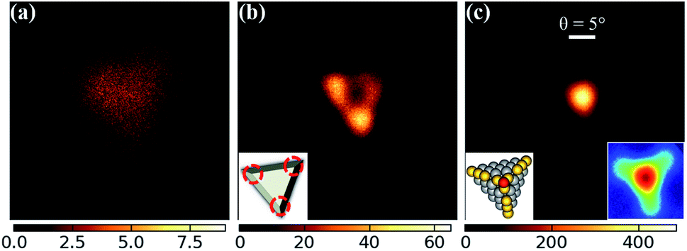 | ||
| Fig. 2 Generation of noble metal-covered W(111) SATs through laser annealing. (a) FE pattern of an Ir-plated W(111) tip before heating, recorded at −900 V. The intensity scale is displayed at the bottom. (b) FE pattern indicating the initial formation of a truncated nanopyramid at the tip apex after illumination of the tip with a femtosecond laser beam (average power P = 180 mW, 1020 nm; polarized parallel to the tip axis) for approximately 10 min. The FE pattern was recorded at a smaller tip bias of −800 V after the laser was switched off. Inset: truncated pyramid. The three spots in the FE pattern were due to field emission from the three corners (circled in red) of the top (111) surface. (c) FE pattern indicating the formation of an SAT with one narrow emission spot after laser annealing for another 5 min.; the pattern was recorded at −600 V without laser illumination. Lower right inset: FE pattern of the SAT on a log-intensity scale. Lower left inset: atomic stacking of a nanopyramid ending in a single atom. Although the three atomic ridges defining the pyramid (shown in yellow) also contribute to field emission, the main beam is highly concentrated and has high contrast. | ||
Fig. 3 presents the evolution of the FE pattern during typical tip heating with a focused laser beam and the self-assembly process of a pyramidal SAT. The process began with a three-spotted FE pattern corresponding to the formation of a truncated pyramid (Fig. 3a). The intensity in the center of the three spots gradually increased, and the FE pattern became triangular (Fig. 3b), indicating the build-up of a taller pyramid with a smaller top area. The build-up process continued, and the center emission spot intensified over time (Fig. 3c and d); the FE pattern also revealed weak emission from the three atomic ridges defining the three-sided {211} pyramid. Eventually, a strong emission spot of approximately 3° (FWHM) appeared, indicating the formation of an SAT (Fig. 3e).
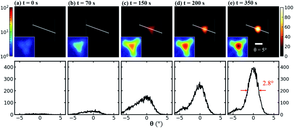 | ||
| Fig. 3 Formation of a pyramidal SAT during laser annealing in a UHV. Top row: FE patterns of an Ir-covered W(111) tip during the laser heating process at various time points. The intensity scale for all FE patterns is displayed on the right. All FE patterns were recorded at a tip bias of −850 V. A femtosecond laser beam (1020 nm; 165 mW, polarized parallel to the axis of the tip) was used for heating. Insets: The FE patterns outlined in the white box are replotted on a log-intensity scale; the intensity scale is displayed on the left. Bottom row: corresponding intensity (linear) profiles along the white line on the top row. The values were calculated by summing the intensity over four pixels in the direction perpendicular to the line. | ||
The appropriate tip temperature to prepare an SAT through laser annealing should be determined; we examined the FE current as a function of the applied tip bias at various laser powers (Fig. 4). The emission current increased when a field-emission tip was irradiated by an ultrafast laser beam. This can be attributed to either multiphoton emission or thermally enhanced FE. The total emission intensity (current) versus time measured using the DLD can be used to identify multiphoton emission, which occurs in burst time,23,24 and the thermally enhanced FE, which exhibits a DC current.30,32Fig. 4a presents an example. A small DC current was observed when no laser illumination occurred at a tip bias of −780 V (shown in black). With laser illumination at a power of 83 mW (shown in red), the DC current increased because of the increase in tip temperature and periodic pulsed signals (due to transient multiphoton emission) separated by 20 ns, corresponding to a laser repetition rate of 50 MHz.
 | ||
| Fig. 4 Derivation of tip temperature during laser illumination. All measurements were performed on the same SAT under the same laser focusing conditions. The SAT was prepared through annealing at a laser power of 165 mW. (a) Electron emission intensity versus flight time measured using a DLD on an Ir-covered W(111) SAT at a tip bias of −780 V without (black) and with (red) irradiation from a femtosecond laser beam (power P = 83 mW, λ = 1020 nm, polarized parallel to the axis of the tip). The increase in the emission current can be ascribed to the thermally enhanced emission (the DC part) and multiphoton field emission (the burst part). (b) The DC part of the emission current versus tip voltage acquired at various laser powers. The black dashed line corresponds to a fit of eqn (1) to measurements without laser illumination (TRT = 300 K), and free parameters were obtained from fitting. The colored dashed lines are the fits of eqn (1) at temperatures of 375, 415, 510, and 645 K. (c) Tip temperature versus average laser power on the basis of fitting in (b). The solid line is a linear fit to the data points. Extrapolation of the fitting line indicates a temperature of approximately 1000 K at a laser power of 165 mW (red square). | ||
The DC current increased with the increase in the applied tip voltage and laser power (i.e., tip temperature); this relationship was used to estimate the tip temperature on the basis of Fowler–Nordheim (F–N) emission (Fig. 4b).39 The FE current density can be calculated as follows:40
 | (1) |
We also discovered that the polarization of laser beams affects the tip temperature (Fig. 5). We defined the relative DC current as the ratio of the DC current under illumination to that without laser illumination. The relative DC values were always more than 1 (Fig. 5a), indicating the presence of a tip-heating effect for all polarization orientations. The DC current was the lowest at parallel polarization (ϕ = 0°) and the highest at perpendicular polarization (ϕ = 90°), which is consistent with the results of other studies.18,19 The tip temperature can be estimated through fitting of the DC part of the emission current versus the tip bias with F–N theory (Fig. 5b). The fitting indicates that the tip temperatures were 780 and 930 K for parallel polarization (red) and perpendicular polarization (blue), respectively. Studies have indicated that the temperature increase for laser illumination of perpendicular polarization is approximately 30% greater than that for parallel polarization,19,20 which is consistent with our measurements. This is because perpendicular polarization matches the excitation condition of plasmonic waves, leading to higher absorbed energy for heating.41 This study indicated that perpendicular polarization is more effective for laser heating of a tip, and a lower laser power is required to reach a desired tip temperature.
 | ||
| Fig. 5 Effects of laser polarization on tip temperature. The measurements were performed on an Ir-covered W(111) SAT at an average laser power of 130 mW. (a) DC part of the electron emission current versus the polarization orientation measured at a tip bias of −870 V. Inset: electric field polarization of the laser beam relative to the tip orientation. (b) DC part of the emission current versus tip voltage without laser illumination (black), with parallel polarization (red), and with perpendicular polarization (blue). The black dashed line corresponds to a fit of F–N theory to measurements at room temperature (300 K). The red and blue dashed lines are fits of F–N theory to measurements at temperatures of 930 and 780 K, respectively. | ||
The structure of a noble metal-covered W(111) SAT might change in a UHV because of the adsorption of residual gas or damage from improper conditions. With laser annealing, a well-defined SAT can be regenerated; regeneration usually requires a few seconds to several minutes, depending on the degree of tip damage and the local laser power. Fig. 6 presents our analysis of an Ir-covered W(111) SAT, which was used in the laser-induced electron emission experiments for 49 days. The SAT might have been damaged accidentally when the laser power at the tip apex was too high. In addition, gas adsorption occasionally occurred at the tip apex. More than 36 laser regenerations were performed. The F–N plots and FE patterns were used to determine the change in the tip sharpness. Fig. 6 displays the FE currents of the regenerated SATs as a function of applied voltage on the 1st, 18th, and 49th days. The data points acquired can be fit to straight lines with similar slopes. Studies have used the slope in F–N plots to determine the sharpness of a FE tip.42–44 Our study indicated that the regenerated SATs changed only slightly over the course of 49 days. The two insets of Fig. 6 present FE patterns with similar intensities acquired on the 1st and 49th days; the voltage on the 1st day was −760 V and it increased slightly to −770 V on the 49th day. These results suggest that a noble metal–covered W(111) SAT can be regenerated hundreds of times through laser annealing, indicating a long lifetime. The SATs also tend to become blunt more quickly when regenerated using a heating loop.6 An advantage of the laser annealing method is that the FE pattern can be monitored in real time during tip heating; thus, minimal heating is applied to regenerate an SAT. For the method involving annealing with a heating loop, the FE pattern can be observed only after annealing to approximately 1000 K for 3–5 min. Although the noble metal–covered W(111) SAT has higher stability than other tip structures, the SAT may change during heating at approximately 1000 K. If no FE pattern of an SAT is observed, the tip requires further annealing.
 | ||
| Fig. 6 F–N plots for SATs regenerated on different days. The plots are based on measurements of the FE currents as a function of tip voltage. The slopes for the best-fit lines on the 1st, 18th, and 49th days are −0.0244, −0.0248 and −0.0256 [μm V−1], respectively. The similarity in the slope indicates that the tip geometry did not change much after 49 days of intensive experimentation. Insets: The FE patterns recorded on the 1st and 49th days corresponding to the data points indicated by the arrows exhibit similar intensity. | ||
We used laser annealing to prepare and regenerate SATs at various laser wavelengths and polarizations, and pyramidal SATs with tips of different radii were generated using pulsed and CW lasers. Fig. S2† presents the regeneration of an Ir-covered W(111) SAT with a femtosecond laser beam with a short wavelength (510 nm, laser power of 150 mW, parallel polarization). Fig. S3† presents the regeneration of a Au-covered W(111) SAT with a CW laser and perpendicular polarization. Pyramidal SATs can be reliably prepared and regenerated in a UHV, indicating the versatility of laser annealing. We noted that in addition to laser power and polarization, the tip temperature was sensitive to focusing conditions such as the focusing spot size and the position of the center relative to the tip apex. The tip apex melted when the tip temperature was too high; the SAT could still be regenerated in most cases but with a blunt tip. However, some SATs could not be regenerated when electric arcing destroyed the tip or when the tip made physical contact with an object; with caution, these accidents can be avoided.
The preparation of well-defined SATs through laser annealing is useful in numerous fields. STM typically requires an SAT to achieve atomic resolution, but atomically sharp tips usually have a unique electronic structure that strongly deviates from the constant density of states (versus energy around the Fermi level) assumed in theoretical modeling.8,45–48 If a well-defined SAT is used, the tip's electronic structure can be characterized and used in the deconvolution of surface electronic structures from scanning tunneling spectroscopy measurements, which would not be possible with the typical SATs used in STM. In STM, the tip is firmly attached to a rigid solid structure to achieve high mechanical stability. The heating loop used in the conventional preparation of noble metal-covered W(111) SATs is incompatible with STM because of its poor mechanical stability; thus, laser annealing provides a convenient method to prepare or regenerate well-defined SATs in STM. SATs are also desirable for UHV-AFM involving a qPlus sensor,49 for which a short tip is glued to the free end of one prong of a quartz tuning fork with epoxy; the sensor cannot tolerate high-temperature heating. To achieve atomic resolution in AFM, the tip should be atomically sharp, which is difficult to achieve. The noble metal-covered W(111) SAT prepared through laser annealing can be an excellent probe for UHV-AFM.
They can also be emitters for electron beams. Conventional emitters mounted on a heating loop have source sizes that are beyond the atomic scale, even if SATs are used. With laser annealing, the tip can be mounted on a firm structure, as in STM, to create an atomically sized source. In addition, the lifetime of SATs is longer than that of state-of-the-art electron sources. In normal use (without illumination from a high-power laser), SATs can typically be maintained for 2–3 weeks under vacuum conditions of 1–3 × 10⁻¹⁰ torr and for months under optimal vacuum conditions. The tip can be regenerated hundreds of times through laser annealing, and a lifetime of at least several years can be expected. Our study also indicated that SATs can be excellent emitters for ultrafast electrons; more details will be presented elsewhere.
SATs are also excellent emitters for gas field ion sources (GFISs).6,50,51 Laser annealing offers advantages in the design of GFIS guns. The emitters of GFISs are usually used at cryogenic temperatures to create high gas ion currents. Adequate thermal conduction between the cryostat and tip is essential, but this causes problems if a heating loop with a thin wire is used. A short heating loop can conduct heat effectively, but the tip would be more difficult to heat to prepare or regenerate SATs. Laser annealing heats only the tip apex; the heating loop can be removed for efficient thermal conduction between the tip and cryostat. Mechanical stability can also be increased, and gun design can be simplified.
4 Conclusions
We demonstrated that laser annealing in a UHV can reliably and effectively prepare and regenerate noble metal–covered W(111) SATs that have well-defined atomic stacking at the apex, and these SATs are thermally and chemically stable. The tip temperature for preparation and regeneration of SATs was determined to be approximately 1000 K. SATs were generated and regenerated at various laser wavelengths (visible or near infrared), with pulsed and CW lasers, and under different polarization conditions. Polarization perpendicular to the long axis of the tip heats the tip more effectively than parallel polarization does. Laser annealing facilitates the generation and regeneration of SATs, thereby enabling the use of SATs in various applications.Author contributions
Tzu-Chieh Yen: methodology, investigation, formal analysis, software, writing – original draft. Wun-Cin Huang: investigation, validation. Chun-Yueh Lin: methodology, resources. Ming-Chang Chen: conceptualization, methodology, supervision, resources, writing – review & editing. Kung-Hsuan Lin: conceptualization, methodology, supervision, resources, writing – review & editing. Ing-Shouh Hwang: conceptualization, methodology, supervision, funding acquisition, writing – original draft.Conflicts of interest
There are no conflicts to declare.Acknowledgements
This research was supported by Academia Sinica [AS-TP-108-M02 (I.-S. Hwang)] and the Ministry of Science and Technology [MOST 110-2112-M-001-060 (K.-H. Lin); MOST 110-2628-M-007-002 and MOST 111-2811-M-007-012 (M.-C. Chen)] of Taiwan. We would like to thank Dr C.-C. Lee in mRadian Femto Sources Co., Ltd for his help in building the Yb-fiber femtosecond laser.References
- H.-W. Fink, Phys. Scr., 1988, 38, 260–263 CrossRef CAS.
- C.-C. Chang, H.-S. Kuo, I.-S. Hwang and T. T. Tsong, Nanotechnology, 2009, 20, 115401 CrossRef PubMed.
- I.-S. Hwang, H.-S. Kuo, C.-C. Chang and T. Tsong, J. Electrochem. Soc., 2009, 157, 7–12 CrossRef.
- H.-S. Kuo, I.-S. Hwang, T.-Y. Fu, J.-Y. Wu, C.-C. Chang and T. T. Tsong, Nano Lett., 2004, 4, 2379–2382 CrossRef CAS.
- T. Ishikawa, T. Urata, B. Cho, E. Rokuta, C. Oshima, Y. Terui, H. Saito, A. Yonezawa and T. T. Tsong, Appl. Phys. Lett., 2007, 90, 143120 CrossRef.
- H.-S. Kuo, I.-S. Hwang, T.-Y. Fu, Y.-C. Lin, C.-C. Chang and T. T. Tsong, Jap. J. Appl. Phys., 2006, 45, 8972–8983 CrossRef CAS.
- H.-W. Fink, IBM J. Res. Dev., 1986, 30, 460–465 CAS.
- V. T. Binh, S. T. Purcell, N. Garcia and J. Doglioni, Phys. Rev. Lett., 1992, 69, 2527–2530 CrossRef.
- V. T. Binh and N. García, Ultramicroscopy, 1992, 42–44, 80–90 CrossRef.
- K.-J. Song, R. A. Demmin, C. Dong, E. Garfunkel and T. E. Madey, Surf. Sci., 1990, 227, L79–L85 CrossRef CAS.
- K. J. Song, C. Z. Dong and T. E. Madey, Langmuir, 1991, 7, 3019–3026 CrossRef CAS.
- T. E. Madey, J. Guan, C.-H. Nien, C.-Z. Dong, H.-S. Tao and R. A. Campbell, Surf. Rev. Lett., 1996, 03, 1315–1328 CrossRef CAS.
- T. Madey, C.-H. Nien, K. Pelhos, J. Kolodziej, I. Abdelrehim and H.-S. Tao, Surf. Sci., 1999, 438, 191–206 CrossRef CAS.
- T.-Y. Fu, L.-C. Cheng, C.-H. Nien and T. T. Tsong, Phys. Rev. B: Condens. Matter Mater. Phys., 2001, 64, 113401 CrossRef.
- H. T. Jeng, H.-S. Kuo, I.-S. Hwang and T. T. Tsong, Phys. Rev. B: Condens. Matter Mater. Phys., 2010, 81, 155424 CrossRef.
- M. Deschler, Z. Agnew. Phys., 1961, 13, 445 Search PubMed.
- C. M. Verber and A. H. Adelman, Appl. Phys. Lett., 1963, 2, 220–222 CrossRef CAS.
- F. F. Kormendi, J. Phys. E: Sci. Instrum., 1974, 7, 1004–1006 CrossRef.
- M. J. G. Lee, R. Reifenberger, E. S. Robins and H. G. Lindenmayr, J. Appl. Phys., 1980, 51, 4996–5006 CrossRef CAS.
- K. W. Hadley, P. J. Donders and M. J. G. Lee, J. Appl. Phys., 1985, 57, 2617–2625 CrossRef.
- Y. Gao and R. Reifenberger, J. Vac. Sci. Technol., A, 1986, 4, 1289–1293 CrossRef CAS.
- M. J. G. Lee and E. S. Robins, J. Appl. Phys., 1989, 65, 1699–1706 CrossRef CAS.
- M. Brugat and M. J. Hagmann, Ultramicroscopy, 1999, 79, 181–188 CrossRef CAS.
- H. Yanagisawa, V. Zadin, K. Kunze, C. Hafner, A. Aabloo, D. E. Kim, M. F. Kling, F. Djurabekova, J. Osterwalder and W. Wuensch, APL Photonics, 2016, 1, 091305 CrossRef.
- B. Rethfeld, A. Kaiser, M. Vicanek and G. Simon, Phys. Rev. B: Condens. Matter Mater. Phys., 2002, 65, 214303 CrossRef.
- P. Hommelhoff, C. Kealhofer and M. A. Kasevich, Phys. Rev. Lett., 2006, 97, 247402 CrossRef PubMed.
- P. Hommelhoff, Y. Sortais, A. Aghajani-Talesh and M. A. Kasevich, Phys. Rev. Lett., 2006, 96, 077401 CrossRef.
- C. Ropers, D. R. Solli, C. P. Schulz, C. Lienau and T. Elsaesser, Phys. Rev. Lett., 2007, 98, 043907 CrossRef CAS PubMed.
- B. Gault, A. Vella, F. Vurpillot, A. Menand, D. Blavette and B. Deconihout, Ultramicroscopy, 2007, 107, 713–719 CrossRef CAS PubMed.
- B. Barwick, C. Corder, J. Strohaber, N. Chandler-Smith, C. Uiterwaal and H. Batelaan, New J. Phys., 2007, 9, 142 CrossRef.
- E. R. Jones, W. C. Huang, G. Basnet, B. N. Flanders and H. Batelaan, Appl. Phys. Lett., 2018, 112, 263104 CrossRef.
- H. Yanagisawa, et al. , APL Photonics, 2016, 1, 091305 CrossRef.
- C. Kealhofer, S. M. Foreman, S. Gerlich and M. A. Kasevich, Phys. Rev. B: Condens. Matter Mater. Phys., 2012, 86, 035405 CrossRef.
- D. Ehberger, J. Hammer, M. Eisele, M. Krüger, J. Noe, A. Högele and P. Hommelhoff, Phys. Rev. Lett., 2015, 114, 227601 CrossRef PubMed.
- T. Wang, J. Guo, J. Shao, D. Wang, A. Chen and M. Jin, Phys. Plasmas, 2015, 22, 033106 CrossRef.
- M. Müller, V. Kravtsov, A. Paarmann, M. B. Raschke and R. Ernstorfer, ACS Photonics, 2016, 3, 611–619 CrossRef.
- W.-T. Chang, I.-S. Hwang, M.-T. Chang, C.-Y. Lin, W.-H. Hsu and J.-L. Hou, Rev. Sci. Instrum., 2012, 83, 083704 CrossRef PubMed.
- A. Oelsner, O. Schmidt, M. Schicketanz, M. Klais, G. Schönhense, V. Mergel, O. Jagutzki and H. Schmidt-Böcking, Rev. Sci. Instrum., 2001, 72, 3968–3974 CrossRef CAS.
- R. H. Fowler and L. Nordheim, Proc. R. Soc. London, Ser. A, 1928, 119, 173–181 CAS.
- K. Jensen, Introduction to the Physics of Electron Emission, John Wiley & Sons Ltd, 2018, pp. 127–133 Search PubMed.
- J. B. Herzog, M. W. Knight and D. Natelson, Nano Lett., 2014, 14, 499–503 CrossRef CAS PubMed.
- A.-S. Lucier, H. Mortensen, Y. Sun and P. Grütter, Phys. Rev. B: Condens. Matter Mater. Phys., 2005, 72, 235420 CrossRef.
- R. J. Behm, N. García and H. Rohrer, Scanning tunneling microscopy and related methods, Springer Science & Business Media, 2013, vol. 184, p. 409 Search PubMed.
- J. Meyer, S. Stranick, J. Wang and P. Weiss, Ultramicroscopy, 1992, 42, 1538–1541 CrossRef.
- J. P. Pelz, Phys. Rev. B: Condens. Matter Mater. Phys., 1991, 43, 6746–6749 CrossRef.
- C. J. Chen and W. F. Smith, Am. J. Phys., 1994, 62, 573–574 CrossRef.
- Y. Gohda and S. Watanabe, Phys. Rev. Lett., 2001, 87, 177601 CrossRef CAS PubMed.
- H.-T. Jeng, H.-S. Kuo, I.-S. Hwang and T. T. Tsong, Phys. Rev. B: Condens. Matter Mater. Phys., 2010, 81, 155424 CrossRef.
- F. J. Giessibl, Rev. Mod. Phys., 2003, 75, 949–983 CrossRef CAS.
- H.-S. Kuo, I.-S. Hwang, T.-Y. Fu, Y.-H. Lu, C.-Y. Lin and T. T. Tsong, Appl. Phys. Lett., 2008, 92, 063106 CrossRef.
- W.-C. Lai, C.-Y. Lin, W.-T. Chang, P.-C. Li, T.-Y. Fu, C.-S. Chang, T. T. Tsong and I.-S. Hwang, Nanotechnology, 2017, 28, 255301 CrossRef.
Footnote |
| † Electronic supplementary information (ESI) available. See https://doi.org/10.1039/d2na00267a |
| This journal is © The Royal Society of Chemistry 2022 |