
 Open Access Article
 This Open Access Article is licensed under a Creative Commons Attribution-Non Commercial 3.0 Unported Licence
Flexible and transparent electrodes imprinted from metal nanostructures: morphology and opto-electronic performance†
Lukas F.
Engel
 b,
Lola
González-García
*b and
Tobias
Kraus
*ab
b,
Lola
González-García
*b and
Tobias
Kraus
*ab
aColloid and Interface Chemistry, Saarland University, Campus D2 2, 66123 Saarbrücken, Germany. Tel: +49 (0)681-9300-389
bINM – Leibniz Institute for New Materials, Campus D2 2, 66123 Saarbrücken, Germany. E-mail: tobias.kraus@leibniz-inm.de; lola.garcia@leibniz-inm.de; Tel: +49 (0)681-9300-269
First published on 5th July 2022
Abstract
We directed the self-assembly of nanoscale colloids via direct nanoimprint lithography to create flexible transparent electrodes (FTEs) with metal line widths below 3 μm in a roll-to-roll-compatible process. Gold nanowires and nanospheres with oleylamine shells were imprinted with soft silicone stamps, arranged into grids of parallel lines, and converted into metal lines in a plasma process. We studied the hierarchical structure and opto-electronic performance of the resulting grids as a function of particle geometry and concentration. The performance in terms of optical transmittance was dominated by the line width. Analysis of cross-sections indicated that plasma sintering only partially removed the insulating ligands and formed lines with thin conductive shells and a non-conductive core. We provide evidence that the self-assembly of high-aspect nanowires can compensate for defects of the stamp and substrate irregularities during imprinting, while spheres cannot. The wire-based electrodes thus outperformed the sphere-based electrodes at ratios of optical transmittance to sheet resistance of up to ≈ 0.9% Ωsq−1, while spheres only reached ≈ 0.55% Ωsq−1.
1 Introduction
Solar cells, light-emitting diodes, and other devices that convert between photons and excitons require transparent conductive electrodes. They are often based on thin films of noble metals, indium tin oxide, semiconductor polymers or hybrids, networks of graphene or carbon nanotubes, metal nanowires, or metal grids.1,2 All of them can be used to create flexible transparent electrodes (FTEs) on thin, flexible and transparent polymer substrates, with performances that depend on the material and the layer morphology.Metal grids are particularly cost-effective transparent electrodes that can be customized:3 their sheet resistance and optical transmittance are defined by the chosen grid geometry and vary with pattern, pitch, conductor width, and conductor thickness.4 Foldable high resolution displays, for instance, require FTEs with a large density of separate, parallel conductors to control the individual pixels. This can be realized with a dense grid of very narrow lines that provide high optical transmittances. The thickness of the lines can be tuned to achieve a conductive cross section that yields an acceptable sheet resistance. Both requires a process that can pattern dense, narrow lines.
E-beam lithography offers the necessary resolution but has a low throughput.5 Printing techniques have been reported to improve fabrication speed. Many are limited to line widths above several micrometers, requiring large pitches to attain transparency. Zhu et al.6 combined an electric-field-driven microscale 3D printing technique with a hybrid hot-embossing process to fabricate Ag-based square grid FTEs with sheet resistances of 0.75 Ωsq and optical transmittances of T500 ≈ 85.79% at a line width of 10 μm and a pitch of 1000 μm. Wang et al.7 report sheet resistances of 0.86 Ωsq and optical transmittances of T500 ≈ 91.26% at a line width of 18 μm and a pitch of 800 μm for their Ag-based square grid FTEs fabricated via ultra-fast laser direct writing. Le Zhao et al.8 demonstrate FTEs based on Cu/Ni square grids, fabricated using lithography and electroplating. They achieved sheet resistances of 0.13 Ωsq and optical transmittances of T500 ≈ 86% at a line width of 8 μm and a pitch of 170 μm. Zhou et al.9 inkjet printed Ag-based square grid FTEs with sheet resistances of 9.56 Ωsq and optical transmittances of T500 ≈ 64.05% at a line width of 46.2 μm and a pitch of 200 μm. Li et al.10 screen printed Ag-based honeycomb FTEs with sheet resistances of 27 Ωsq and optical transmittances of T500 ≈ 67% at a line width of 200 μm and a pitch of 1040 μm. Scraping is an alternative 5-step process where the electrode material is spread across a previously prepared substrate pre-patterned with recesses and can yield 3 μm wide lines, for example.11
Nanoimprinting combined with self-assembly provides an efficient 2-step route to grids of sub-micron metal lines.12–18 Dispersions of metallic nanocolloids (colloidal inks) can be imprinted under ambient conditions in a roll-to-roll compatible process with a patterned polymer stamp that is being rolled over the substrate.19,20 The colloidal ink is confined in the stamps' cavities and the solvent permeates through the polymer. The dispersed particles self-assemble into features defined by the stamp. Particle geometry and concentration can be tuned to affect self-assembly and the resulting structures.20 Metallic nanocolloids often carry organic ligand shells that prevent agglomeration and have to be removed after imprinting, for example in a plasma.21
Maurer et al.19 nanoimprinted self-assembling Au nanowires with a core diameter of 1.6 nm, an aspect ratio on the order of 103, and an oleylamine ligand shell. The wires self-assembled into bundles inside the square grid defined by the stamp. The resulting grid was sintered using a low-pressure, room temperature plasma treatment that retained the overall geometry and did not damage the thin polymer substrate. The resulting FTEs had sheet resistances of 128 Ωsq/196 Ωsq (in printing direction/perpendicular) and optical transmittances of T500 ≈ 86% at line widths of 1.41 μm/0.91 μm and a pitch of 19.5 μm.19 Kister et al. imprinted Au nanospheres with a core diameter of 3.2 nm and C4-, C8- or C12-thiols or amines. Both reports used the same printing method that we study here, but different process parameters and particle ligands. The best-performing FTEs formed from particles with dodecylamine ligand shells and had sheet resistances of 150 Ωsq and optical transmittances of T500 ≈ 91% at line widths < 1 μm and a pitch of 19.5 μm.20 The basic functionality of such nanoimprinted electrodes was demonstrated by integrating them into capacitive and resistive touch devices.19 Other examples for the integration of nanoimprinted electrodes into functional devices include organic field effect transistors,13,15 nanobatteries22 and flexible organic light-emitting devices.23
The structure–property relations between the morphology of metal conductors formed during nanoimprinting and the opto-electronic electrode performance are not fully understood. There are, however, some studies on spin-coated, inkjet-printed and drop-casted nanoparticle assemblies and the effect of plasma sintering on their morphology and/or sheet resistance. Shaw et al.24 investigated crack formation in spin-coated assemblies of ligand-capped colloids (varying in composition, shape, size and ligand as well as the used solvent) on Si substrate during drying, O2 plasma-induced ligand removal, and thermal sintering. They found that close-packed and ordered particle packing always led to cracking, while disordered particle films with thicknesses up to 440 nm remained crack-free. Reinhold et al.25 studied the effect of Ar plasma sintering on the morphology and resistivity of inkjet printed tracks (Ag nanoparticles with a diameter of 5 to 10 nm in tetradecane) on polymer substrates. They report the formation of a conductive Ag skin layer and a non-conductive core. The skin layer thickness was independent of the printed layer thickness and increased with plasma treatment time before saturating. Ma et al.26 investigated the effect of Ar plasma sintering on the morphology of drop-casted layers of Ag nanoparticles (gum arabicum capped, 23 nm and 77 nm in diameter, dispersed in DI water) on glass and the resulting sheet resistance. Plasma sintering converted discrete particles to a more continuous film with time, and increasing RF power accelerated this transition. A simple parallel circuit model was formulated based on a fully sintered skin layer and a less or non-conductive core. Assuming a non-conductive core, the calculated skin layer resistivities matched the morphological development with increasing plasma sintering time and increasing RF power well.
Here, we study the effects of particle shape and superstructure formation on the conductor morphology and opto-electronic performance. Au nanowires (wires) and Au nanospheres (spheres) were imprinted as grids of parallel lines with a width of about 1.6 μm and a pitch of 19.5 μm at different Au concentrations cAu on polyethylene terephthalate (PET) foil. The lines underwent H2/Ar plasma sintering. We quantified the performances of the resulting transparent electrodes using a figure of merit (FOM) and compared them to the electrode morphologies before and after plasma sintering. We found that wires form lines with a coarse surface microstructure and pronounced bleeding, while spheres form smooth lines with less bleeding. The plasma formed a conductive shell and a non-conductive core for both particle types, with the thicker shell in case of the spheres. Electrode performance was dominated by defect densities, where wires outperformed spheres because they better bridged stamp and substrate irregularities during imprinting. The FOM always increased with increasing cAu, but the FOM with wires was at least 3.4 times higher at any given cAu.
2 Materials and methods
2.1 Synthesis of Au nanowires/-spheres
In a typical AuNW synthesis, 60 mg of HAuCl4·3H2O (10 mM) were weighed into a disposable 50 mL glass snap-on vial from Carl Roth GmbH + Co. KG (Karlsruhe, Germany). Then, 9.9 mL of n-hexane and 2.04 mL of oleylamine (400 mM) were added. The mixture was vortexed for 1 min to fully dissolve the Au acid. Then, 3.06 mL (1 M) of triisopropylsilane (TIPS) were added as reducing agent. The solution was vortexed for 30 s and kept in an oven at 25 °C for 24 h without any mechanical agitation.
The highly hygroscopic HAuCl4·3H2O was weighed in dry in a glove box from SylaTech GmbH (Walzbachtal, Germany) because the presence of water results in shorter wires.31 The reaction vessel was filled with dry Ar. OAm acts both as ligand and as reducing agent, albeit weaker than TIPS. OAm and TIPS were added in that order using a 5 mL pipette. The interval between injections was minimized to avoid reduction in the absence of TIPS.
In a typical AuNP synthesis, 200 mg of HAuCl4·3H2O were weighed into a disposable 100 mL glass snap-on vial from Carl Roth GmbH + Co. KG (Karlsruhe, Germany) under ambient conditions because the synthesis is less water sensitive. Then, 16 mL of pentane and 16 mL of OAm were added. The mixture was stirred at 500 rad min−1 and room temperature for 45 min (solution A). In the meantime, 80 mg of tert-butylamine borane were dissolved in a mixture of 4 mL pentane and 4 mL OAm (solution B). After precisely 45 min (the waiting time determines the sphere diameter), solution B was added to solution A and the color turned immediately dark brown. Then the mixture was stirred for another 60 min with a loose lid.
The purification of AuNP was similar, but with centrifugation at 3435 rcf and 5 min for the first and 3435 rcf and 60 min for the second step. The AuNP were re-dispersed to cAu ≈ 30 mg mL−1.
Other ink concentrations were produced through dilution of the respective stock dispersion. AuNW inks were stored in a fridge at 5 °C, AuNP inks were stored at room temperature for 16 h before usage.
2.2 Small-angle X-ray scattering (SAXS)
Sphere diameter and dispersion state were characterized via SAXS. The dispersion was transferred to glass mark-tubes from Hilgenberg GmbH (Malfeld, Germany) with an inner diameter of 1.5 mm. The tubes were sealed with a fast-curing two-component epoxy from R&G Faserverbundwerkstoff GmbH (Waldenbuch, Germany) to prevent solvent evaporation.The scattering setup, a Xeuss 2.0 HR SAXS/WAXS instrument from Xenocs SAS (Grenoble, France) used a Cu Kα source and a detector PILATUS3 R 1 M from DECTRIS AG (Baden, Switzerland) at a distance of about 550 mm from the samples. The distance was calibrated with a Ag behenate sample before each measurement. Each sample was measured for a total of 30 min. The two-dimensional scattering images were azimuthally integrated with the software Foxtrot from Synchrotron SOLEIL (Saint-Aubin, France) to obtain the scattering curves. The solvent background was measured separately and subtracted. To determine the average sphere diameter, fitting of the scattering curves was performed with the software SASfit from the Laboratory for Neutron Scattering at Paul Scherrer Institute (Villigen, Switzerland).
2.3 Nanoimprinting
Silanization was performed directly on the silicon master and after plasma activation of the PDMS master for 1.5 min using an oxygen plasma at 0.3 mbar in a low pressure plasma reactor of type Pico from Diener electronic GmbH & Co. KG (Ebhausen, Germany). Silanization took place inside a conventional glass desiccator with a snap-on vial cap containing 30 μL of (tridecafluoro-1,1,2,2-tetrahydrooctyl)trichlorosilane from abcr GmbH (Karlsruhe, Germany). The vial was shielded from the masters to increase uniformity. The desiccator was flushed with Ar, evacuated to 3 mbar, and disconnected from the vacuum pump. After 30 min, the desiccator was slowly ventilated with air.
PDMS base and curing agent, Sylgard 184 from Dow Inc. (Midland, USA), were mixed in a 10![[thin space (1/6-em)]](https://www.rsc.org/images/entities/char_2009.gif) :1 (w/w) ratio and degassed in a Speedmixer DAC 600.2 VAC-P from Hauschild GmbH & Co. KG (Hamm, Germany) at a speed of 2350 rpm and a pressure of 1 mbar for 3 min. The mixture was poured onto the respective master with a Teflon spacer ring (2 mm thick) and a glass plate as top sealing. The PDMS was fully cured at 80 °C for 3 h and the replica were carefully peeled off along the stamp channels.
:1 (w/w) ratio and degassed in a Speedmixer DAC 600.2 VAC-P from Hauschild GmbH & Co. KG (Hamm, Germany) at a speed of 2350 rpm and a pressure of 1 mbar for 3 min. The mixture was poured onto the respective master with a Teflon spacer ring (2 mm thick) and a glass plate as top sealing. The PDMS was fully cured at 80 °C for 3 h and the replica were carefully peeled off along the stamp channels.
Imprinting stamps were cut into two parts with an area of 3.5 cm × 8 cm of which 3.5 cm × 7 cm were patterned. Larger areas can be printed using the complete imprinting stamp.19 The flat 3.5 cm × 0.5 cm at either end of the stamp served as run-in and run-out areas during imprinting.
2.4 Plasma sintering
Plasma sintering was performed in a low pressure 13.56 MHz RF plasma reactor of type Pico from Diener electronic GmbH & Co. KG (Ebhausen, Germany) immediately after nanoimprinting. Ar/H2 (95% Ar and 5% H2) was used as process gas. The procedure was carried out at room temperature and ≈ 0.3 mbar for 20 min with 100 W RF power.2.5 Sheet resistance measurements
Sheet resistances were determined in a 2-point-probe configuration using a multi-channel multi-meter (DAQ6510 data acquisition logging multi-meter system) equipped with multiplexer cards (7702 40-channel differential multiplexer module with screw terminals) from Keithley Instruments GmbH (Germering, Germany). The electrodes were contacted using a fast drying Ag paste ACHESON Ag DAG 1415 from Plano GmbH (Wetzlar, Germany) and AGF 1 miniature crocodile clamps from SKS Kontakttechnik GmbH (Niederdorf, Germany). Ag paste was applied in two parallel lines, each 1.5 cm long and spaced 1.5 cm apart, resulting in a square measurement field. The determined resistances corresponded directly to the desired sheet resistances.2.6 UV-vis spectroscopy
The optical transmittance of the electrodes was determined with a Cary 5000 UV-vis-NIR spectrophotometer from Agilent Technologies Deutschland GmbH (Waldbronn, Germany) with a tungsten halogen light source for the visible range and a deuterium arc light source for the UV range. The samples were mounted behind blackened metal masks with circular apertures (5 mm in diameter). Measurements were performed in double-beam mode against air at scan rates of 600 nm min−1. The samples were placed such that the blank sides were in contact with the mask to prevent any damage to the electrodes on the other side. Baselines of bare PET substrates were recorded as references.2.7 Confocal laser scanning microscopy (CLSM)
The electrodes' surface topographies were characterized using a MarSurf CM explorer from Mahr AG (Thalwil, Switzerland) at 100-fold magnification, which corresponded to a measuring field of about 161 μm by 161 μm. The vertical resolution was 2 nm, the lateral resolution 320 nm, effectively allowing for data points every ≈ 130 nm. For a single topography map, 1240 equidistant height traces across eight parallel conductor segments were acquired. Data analysis was performed with Python (Anaconda distribution) as described below. Note that CLSM overestimates the height of the material at the edge of the lines, blurring the edge. We thus detected the edge with a slope-based (m) termination criterion (absolute values of m: |mwires| ≤ 0.03 and |mspheres| ≤ 0.06) for both S-shaped sides of the Gaussian conductor profile.2.8 Cross-sectioning via focused ion beam (FIB)
The conductor cross sections were prepared using a FEI Versa 3D DualBeam from Thermo Fisher Scientific GmbH (Schwerte, Germany). The conductors were protected by subsequently deposited layers of Pt using the electron beam first, then the ion beam.2.9 Transmission electron microscopy (TEM)
Dry particle samples were prepared by diluting AuNW and AuNP dispersions to concentrations of approximately 0.1 mg mL−1 and drop-casting 3 μL on a carbon-coated copper grid from Plano GmbH (Wetzlar, Germany). All samples were characterized at an acceleration voltage of 200 kV in a JEM 2010 from JEOL GmbH (Freising, Germany).2.10 Scanning electron microscopy (SEM)
Scanning electron micrographs were recorded using either a FEI Quanta 400 ESEM or a FEI Versa 3D DualBeam from Thermo Fisher Scientific GmbH (Schwerte, Germany) with secondary electron detectors. The electrodes for SEM were imprinted onto polished, p-type silicon wafers from Siegert Wafer GmbH (Aachen, Germany).3 Results and discussion
Fig. 1 illustrates the trade-off between electrical resistance R and optical transmittance T of metal grid-based FTEs. We prepared grids of parallel lines using gold nanosphere (AuNP) and gold nanowire (AuNW) colloids with increasing concentration cAu (three samples per concentration), plasma-sintered them, and compared their average transmittances in the visible range (from 400 nm to 800 nm) to their sheet resistances Rsh. It is convenient to express the overall performances using the Figure of Merit developed by Fraser and Cook,32
 | (1) |
 and the sheet resistance Rsh.
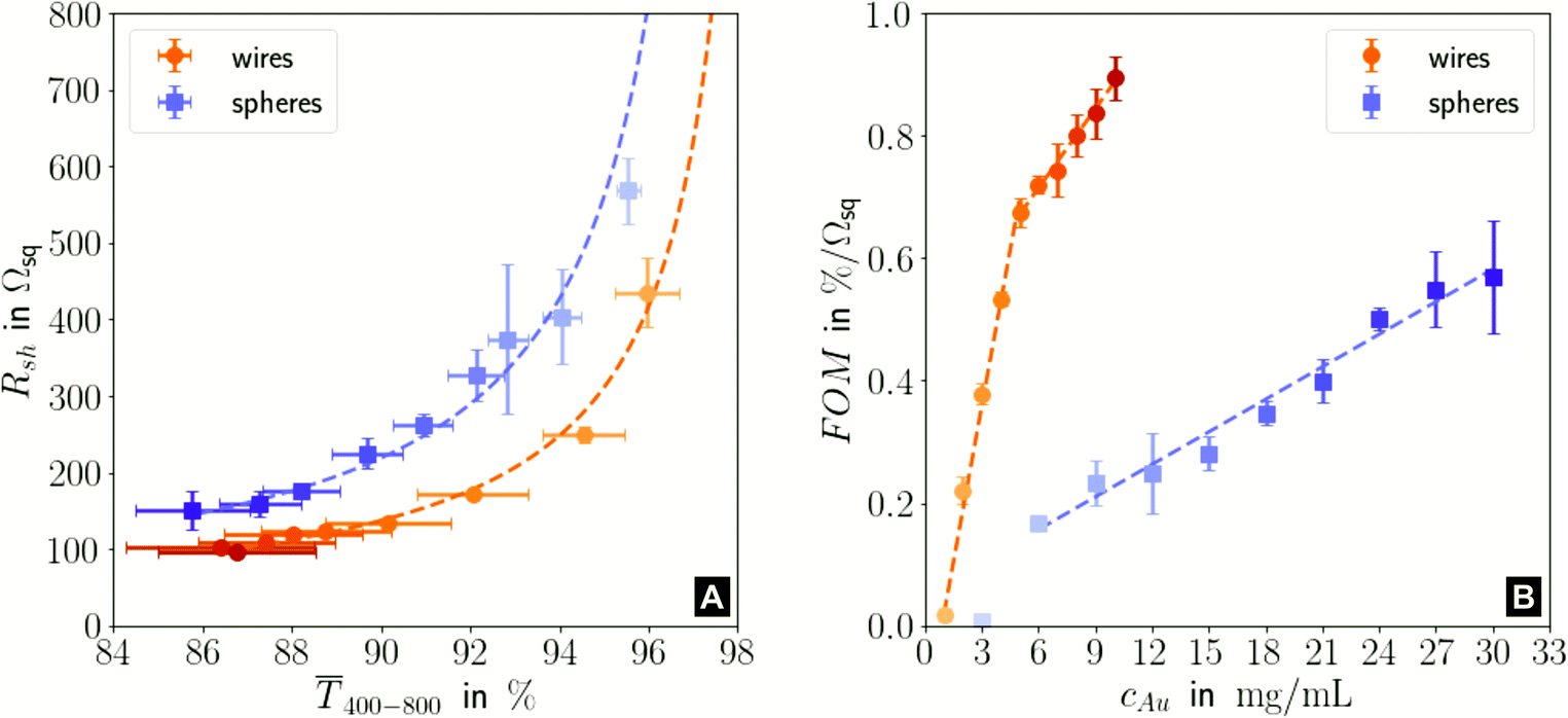 | ||
Fig. 1 (A): Sheet resistances Rsh and optical transmittances  for wire- and sphere-based electrodes directly after plasma sintering. Data for electrodes with Rsh that exceeded the scale are not included (Section 2 of the ESI† has the complete data set). (B): Dependence of for wire- and sphere-based electrodes directly after plasma sintering. Data for electrodes with Rsh that exceeded the scale are not included (Section 2 of the ESI† has the complete data set). (B): Dependence of  with concentration cAu. All graphs show average values from three measurements, the standard deviation, and a fit (dashed lines). Light colours represent the lowest and dark colours the highest Au concentrations in the printed colloids. with concentration cAu. All graphs show average values from three measurements, the standard deviation, and a fit (dashed lines). Light colours represent the lowest and dark colours the highest Au concentrations in the printed colloids. | ||
The concentrations of the colloids were varied in the range of 1–10 mg mL−1 for the wires and 3–30 mg mL−1 for the spheres. The lower limit was set by percolation; the upper limit was set by requiring a minimum optical transmission of 85%. Darker colors in the plots indicate larger concentrations.
Sheet resistance and optical transmittance decreased with increasing cAu for both wires and spheres, but wires always had lower  and Rsh for a given concentration. Functional electrodes could be made from both wires and spheres in the range cAu ∈ 3 to 10 mg mL−1. The FOM for wire-based electrodes in this range was at least 3.4 times larger than that of sphere-based electrodes. Resistances were more sensitive to cAu than transmittances, and the FOM increased with cAu for both nanocolloids. FTEs with the same optical transmittance always had lower Rsh when made from wires. Interestingly, δFOM/δcAu for wire-based electrodes abruptly decreased at cAu ≈ 5 mg mL−1 to 75%. The highest FOM ≈ 0.9% Ωsq−1 of all FTEs in this study was for AuNW at cAu = 10 mg mL−1.
In the following, we analyze the effect of particle shape on grid morphology, starting with nanowires. The wires (Fig. 2A) had a core diameter dw of 1.7 nm28 and lengths lw between 2 μm33 and 6.4 μm34 (aspect ratio on the order of 103). Previous studies have shown that 70% of the wires at the concentrations used here are part of dispersed bundles.35
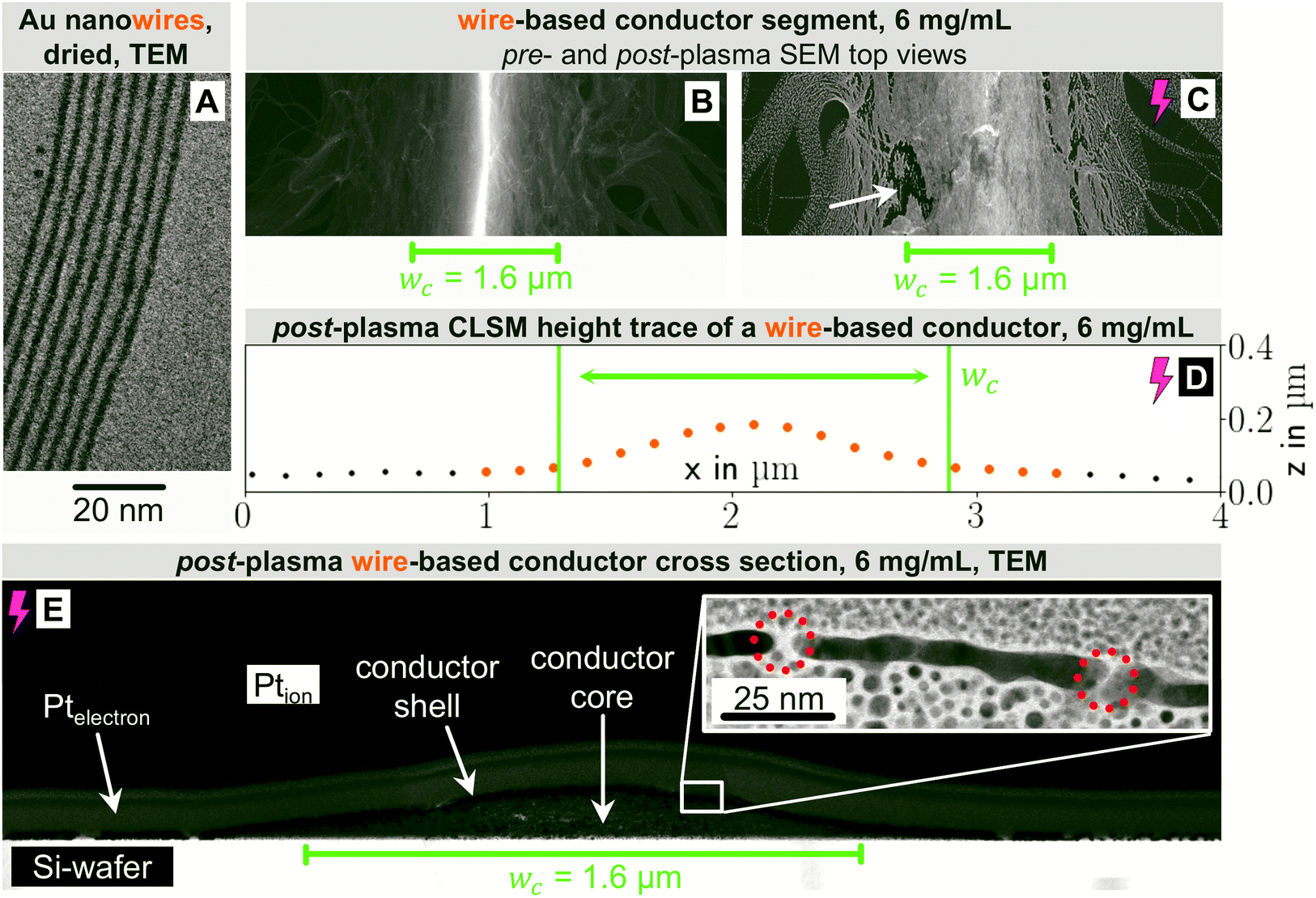 | ||
| Fig. 2 Typical morphological features of lines printed from AuNW at cAu = 6 mg mL−1 before and (purple flash) after plasma. (A): TEM image of dried and self-assembled wires. (B): SEM image (top-view) of a printed line. (C): SEM image (top-view) of a printed, plasma-sintered line; the white arrow indicates one of the typical crack-like defects which start forming at 6 mg mL−1 in the bleeded parts. (D): Height trace of a printed, plasma-sintered line. (E): TEM image of a cross-section of a printed, plasma-sintered line. Inset: A shell formed by the plasma. The red dashed circles indicate gaps within the shell. | ||
Fig. 2 shows top-view electron micrographs of grids imprinted from wire dispersions with cAu = 6 mg mL−1 on doped Si before (B) and after (C) plasma sintering. Approximately 90% of the wires were concentrated and aligned in lines of width wc, the rest exceeded the boundaries (bleeding) and was only partially aligned. A sharp ridge formed in the center of the line. Plasma sintering partially removed the oleylamine and blunted the ridge. The wires in particularly thinly covered areas of the bleeded part fragmented, rendering them non-conductive. Fig. 2D shows the profile of a plasma-sintered line on PET foil obtained from CLSM. The wires formed a flat, Gaussian profile that was wider than the stamp feature, probably because the material flowed when the stamp was removed.
Bundling wires form extended networks.12,19,36 We propose that they are gel-like and cannot be easily displaced by the stamp, which causes further bleeding (Fig. 2B and C). Defects in the conformal stamp-substrate contact due to edge imperfections and reduced contact pressure around the channel edges aggravate the effect.37
Fig. 2E is a transmission electron micrograph of a plasma-treated line on a silicon substrate. The change of the cross-sectional profile during plasma sintering was minor. Only the outermost part of the conductor was fully sintered, resulting in a structure with a metallic Au shell (average thickness tshell = 5.7 ± 1.1 nm) and a hybrid, probably less conductive core. The plasma did not fully penetrate the deposited material, probably because shell formation is self-limiting. This explains why extended plasma sintering barely lowered Rsh. The cross section confirms that material beyond wc contributes to conductivity and suggests that CLSM overestimates the height of the non-conductive areas next to the conductor. The shell of the center part was porous as marked in Fig. 2E, probably due to the AuNW bundle superstructure.
Compare, now, the wire-derived lines to samples formed from spheres. We imprinted Au cores with diameters dsp of about 3.7 nm that were coated with a dense shell of OAm (shell thickness approximately 2 nm) as seen in Fig. 3A. They were fully dispersed according to Small Angle X-ray Scattering (Fig. S3 of the ESI†). Fig. 3 shows top-view electron micrographs of imprinted grids formed at cAu = 30 mg mL−1 on doped silicon before (B) and after (C) plasma sintering. The lines were sharply delineated with little bleeding and a homogeneous surface microstructure. The difference to wires is probably due to the spheres' excellent dispersion state even at high cAu towards the end of the printing process. A ridge formed along the centre that was blunted by the plasma sintering and is no longer visible after plasma sintering. The center line microstructure remained homogeneous after plasma; coalescence and island formation beyond the defined feature did not contribute to conductivity.
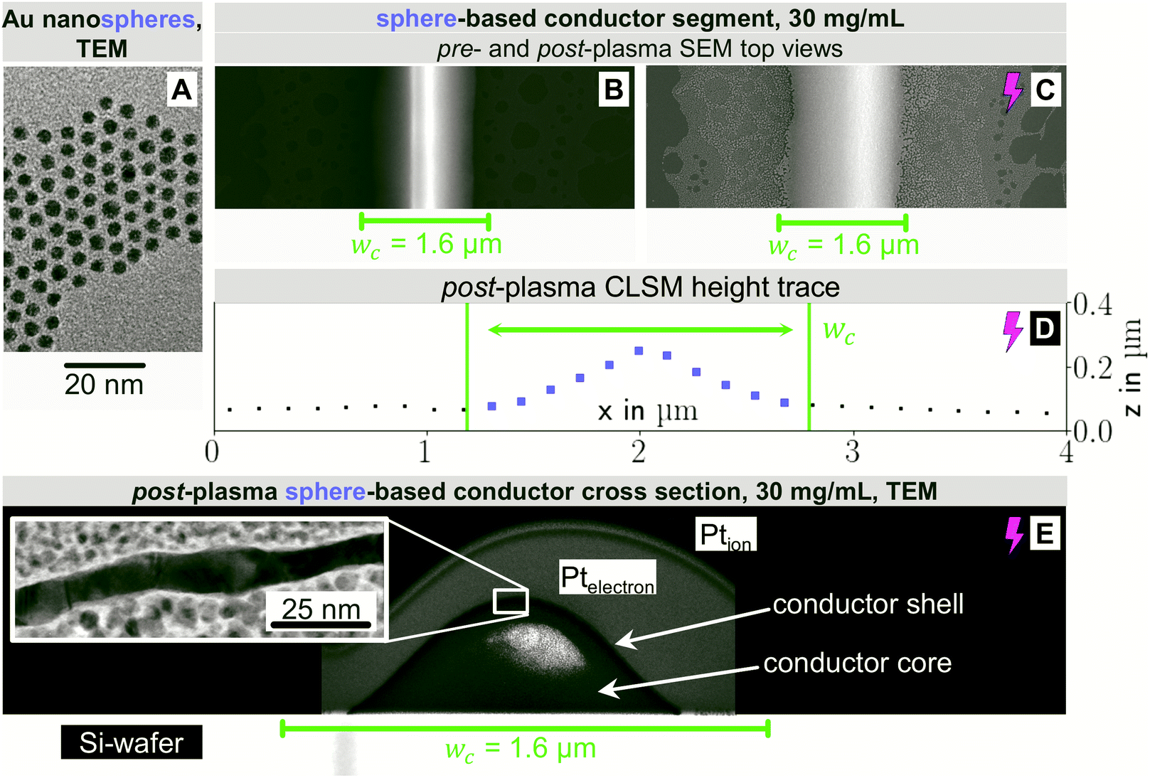 | ||
| Fig. 3 Typical morphological features of lines printed from AuNP at cAu = 30 mg mL−1 before and (purple flash) after plasma. (A): TEM image of dried and self-assembled spheres. (B): SEM image (top-view) of a printed line. (C): SEM image (top-view) of a printed, plasma-sintered line. (D): Height trace of a printed, plasma-sintered line. (E): TEM image of a cross-section of a printed, plasma-sintered line. Inset: A shell formed by the plasma. | ||
Fig. 3D shows the CLSM profile of a plasma-sintered line on PET with a similar Gaussian profile as for nanowires above. Fig. 3E depicts the core–shell structure with a shell thickness tshell = 8.1 ± 1.4 nm, slightly above that for wires, and a non-porous structure. Lines printed at cAu = 12 mg mL−1 had similar features. At lower concentrations, closer to the percolation threshold, pores and disconnected segments formed (Fig. S7 in the ESI†).
In the following, we analyze the effect of particle concentration on the geometry of the printed, plasma-sintered grids. Confocal metrology provided a total of twenty height profiles measured on PET – one at each of the respective ten cAu for both wires and spheres. Fig. 4A and B show topography maps of selected conductor segments, Fig. S4 and S5 of the ESI† show larger areas for the lowest and highest cAu. We detected the edges of printed lines using a slope-based termination criterion (see Materials & Methods Section on CLSM). The cross sections of the shells were calculated by multiplying the average tshell (Section S6 in the ESI†) with the outer contour length. The mean values of w, hmax and Ashell as a function of gold concentration are shown in Fig. 4C, D and E.
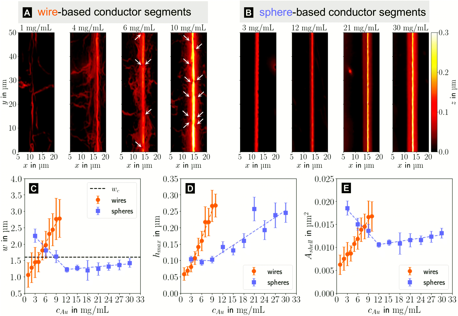 | ||
| Fig. 4 Topography maps of (A) wire- and (B) sphere-based printed lines after plasma sintering. White arrows indicate defects similar to those in Fig. 2C. (C) Average conductor width w, (D) maximum conductor height hmax and (E) cross-sectional area Ashell as a function of gold concentration cAu. Standard deviations are indicated as error bars, the dashed lines are fits by linear regression to better illustrate the (piece-wise) linear behaviour. | ||
The width and height of wire-derived imprinted lines increased with cAu (Fig. 4A). The height of sphere-derived imprinted lines increased with cAu, while their width was maximal at the lowest concentration and minimal at 12 mg mL−1. The difference between wires and spheres is likely due to the different agglomeration mechanisms. A considerable fraction of wires at cAu = 1 mg mL−1 is bundled,35 while spheres are still well dispersed at 30 mg mL−1 (Fig. S3 in the ESI†).
The variation of δw/δcAu for spheres is likely connected to ink viscosity and agglomeration. Low-concentration inks tend to have low viscosities, low contact angles, and longer drying times. They can easily migrate beyond wc before complete solvent evaporation. Higher concentrations increase the viscosity and agglomeration rate, reducing w to below wc. A small fraction of the ink still bleeds, and the highest concentration leads to a perceptible amount of metal deposited beyond wc.
For wires, δhmax/δcAu showed an increase at 3 mg mL−1 which roughly coincided with w reaching wc. This suggests that at lower concentrations, particles can freely assemble into increasingly wide lines. When w reaches wc, additional particles add to the thickness or cause bleeding, and w/hmax drops steadily at 4 mg mL−1 and above (Fig. S9 in the ESI†). A similar change of δhmax/δcAu for spheres at 9 mg mL−1 coincided with the w = wc, too, suggesting the same mechanism.
The cross-sectional area Ashell was almost proportional to w for both wires and spheres (Fig. 4E). This is because tshell is set by the plasma process and practically independent of cAu. The conductor width w ≫ hmax dominates the product tshell · w.
For wires, percolation and electrical conductivity occurred at 2 mg mL−1; crack-like defects appeared at 6 mg mL−1 (white arrows in Fig. 4A), and became denser with increasing cAu. They did not affect w and Ashell but affected the conductivity σshell, which changed sign and slope at 6 mg mL−1 (Fig. 5C).
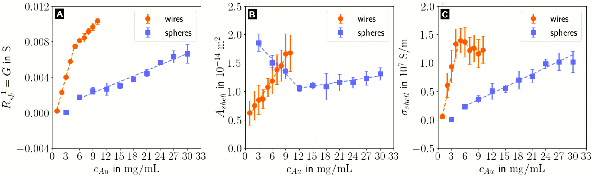 | ||
| Fig. 5 Effect of particle concentration cAu on (A) the conductance G of a representative square electrode sub-section, (B) the cross-sectional area Ashell and (C), the shell conductivity σshell. Standard deviations are indicated as error bars, the dashed lines are fits by linear regression to better illustrate the piece-wise linear relations. | ||
With CLSM, the sphere-derived lines appeared mostly defect-free (due to the limited resolution and field of vision) as shown in Fig. 4B. A detailed analysis indicated, however, that lines formed at low concentrations (3 to 9 mg mL−1) contained large discontinuous segments and exhibited numerous pores (Fig. S7 of the ESI†). Additionally, we found imprinting defects (Fig. S8 in the ESI†) due to tapered or clogged stamp channels and stamp irregularities. They appear less frequently than the cracks in wire-based lines but reduce σshell more drastically because they often affect the entire width of the line and render it non-conductive. We propose that small, dispersed spheres are more susceptible to such defects because their superstructures are more easily disrupted than network-forming, bundling wires. Increasing cAu increases the probability that irregularities are bridged by a thicker particle layer.
The measured macroscopic sheet resistance Rsh of the transparent electrodes is due to the parallel conductivity of 750 parallel printed lines of length l = 1.5 cm. If we assume that only their shells with cross-sectional areas Ashell conduct, the overall sheet resistance is
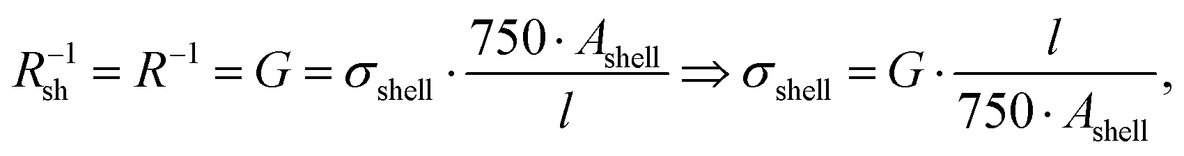 | (2) |
The shell conductivities σshell universally increased with increasing cAu. They remained below one third that of bulk Au (σAu ≈ 4.52 × 10⁷ S m−1).38 The most conductive shells had 1.39 × 10⁷ S m−1 for wire-based and 1.02 × 10⁷ S m−1 for sphere-based line arrays, in the range reported for ultra-thin polycrystalline Au films with thicknesses of 5.5 to 8.0 nm,39 below the electron mean free path of λAu ≈ 37.7 nm.40 This is consistent with a shell-dominated conductivity.
The change of δσshell/δcAu at 5 mg mL−1 for wire-based lines is due to the line width w that exceeds wc (Fig. 4C), accompanied by an increasing number of crack-like defects in the shell as discussed above (Fig. 4A).
The wire-based lines outperformed the sphere-based lines at every cAu despite a thinner (5.66 nm vs. 8.07 nm), porous shell. A possible explanation is the increased defect density in sphere-based lines. It does not affect w, hmax and Ashell, but can render entire lines non-conductive so that they contribute nothing to σshell. A second difference are grain boundary densities in the shells. The wires are micrometer-long single crystals29 and largely oriented in imprinting direction. Their crystallinity may be at least partly retained during plasma sintering,41 while spheres are likely to create small grains. Thirdly, the likelihood that the only partially sintered line core also contributes to conduction, is higher in case of the high aspect ratio wires than in case of the spheres (lw ≫ dsp).
In summary, the electrical properties of both electrode types were dominated by the core/shell structure of its conductors. Defects within the conductor shell and concentration independent shell thicknesses below λAu prevented σshell from reaching bulk Au conductivity. The wires' ability to self-assemble into percolating superstructures even at the lowest concentration used is the basis for the superior performance of wire-derived electrodes.
The printed lines reduce the optical transmittance mainly by masking parts of the substrate. The change in optical transmittance  was always negative for both wires and spheres (Fig. 6A and B). The value was constant for spheres; it changed at 6 mg mL−1 for wires, close to where w exceeded wc (Fig. 4C). Wire-based electrodes had lower optical transmittances; all were above ≈ 85% and thus practically useful.
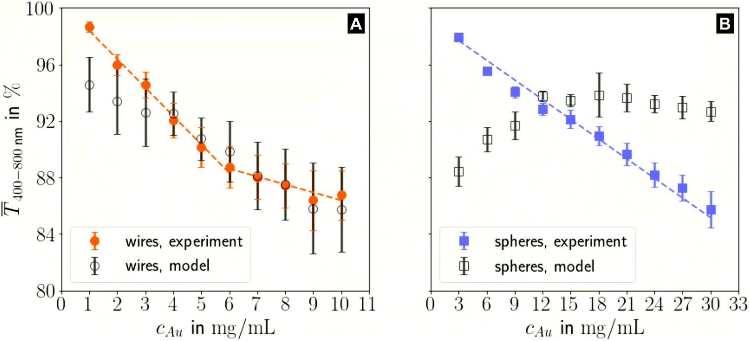 | ||
Fig. 6 Development of the optical transmittance  for (A) wire- and (B) sphere-based electrodes (experiment and model) with concentration cAu, the belonging standard deviation and a data fit (dashed lines). for (A) wire- and (B) sphere-based electrodes (experiment and model) with concentration cAu, the belonging standard deviation and a data fit (dashed lines). | ||
We approximated the metal lines as rectangles of width w at pitch p using data from CLSM measurements (the stamp pitch was p = 19.5 μm). The PET substrate was taken to be transparent and the rectangular lines as opaque. This yields a model transmittance Tmodel (Fig. S10 of the ESI†) of
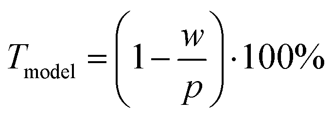 | (3) |
The experimental  for wire-based lines were above Tmodel. (Fig. 6A) up to cAu = 3 mg mL−1. The lines at such low concentrations were narrow but thin (Fig. 4C and D) and likely not fully opaque over the entire width. The lines formed above 4 mg mL−1 had w > wc (Fig. 4C) and became increasingly thicker (Fig. 4D and S9 in the ESI†). This increased their opacity and improved the match between model and experiment in the range 4 to 10 mg mL−1.
The experimental  for sphere-based lines exceeded Tmodel for 3 to 9 mg mL−1. The lines were broad (Fig. 4C) and thin in this range, only growing in thickness at 9 mg mL−1 and above (Fig. 4D and S9 in the ESI†). In contrast to wires, we found that
 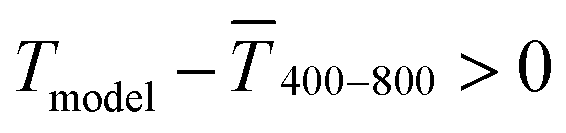 above 12 mg mL−1, probably because the metal that was deposited beyond w (Fig. 3C) caused strong diffuse scattering.
In summary, sphere-based outperformed wire-based electrodes in optical transmittance. Lines formed from spheres at low concentrations were more transparent; lines formed at higher concentrations were narrower. This is likely a direct consequence of the bundling wires' lower percolation threshold that enabled significant material deposition beyond wc, which more than compensated for the increasing bleeding of spheres at high concentrations.
Considering both optical and electrical properties, cAu affected optical transmittance much less than Rsh for both wires and spheres (Fig. 5A). The overall FOM was dominated by the sheet resistance, which explains the better performance of wire-based electrodes (Fig. 1).
4 Conclusion
Flexible transparent electrodes were imprinted from AuNP or AuNW at different concentrations and treated with plasma that partially removed the oleylamine ligand. We found strong correlations between the geometry of the nanocolloid, the concentration used for imprinting, the resulting post-plasma grid morphology, and the opto-electronic performances.Plasma sintering led to a conductor structure with an outer gold shell that covered a hybrid core. The imprinted lines' average conductivity σshell depended on the density of defects in the shell that changed depending on concentration and particle type and rendered some lines discontinuous. Wire-based inks were less prone to such discontinuities and thus outperformed the sphere-based inks. The wires' aspect ratios of above 1000 facilitated their self-assembly into percolating superstructures that bridged stamp and substrate irregularities. This result is interesting for industrial processes that require a robust printing of lines. At concentrations ≥ 6 mg mL−1, an increasing number of crack-like defects occurred within the bleeded parts of wire-based conductors and impaired σshell.
The optical transmittance of wire-based electrodes made with concentrated inks followed a simple model that assumes opaque lines.  of sphere-based electrodes made with concentrated inks was more strongly affected by bleeding that led to areas of partial transmittance. Nevertheless, sphere-based outperformed wire-based electrodes due to a better definition of geometry at high concentrations (7–10 mg mL−1) and due to more transparent lines at lower concentrations (3–6 mg mL−1).
For both wires and spheres, concentration affected  much less than Rsh. The FOM was thus dominated by Rsh, and wire-based electrodes that reached significantly lower Rsh at the same Au content performed better than sphere-based electrodes.
Both wire- and sphere-based electrodes had relatively large non-conductive parts. Their fraction may be reduced by tuning the ligand chemistry and the plasma process. It should be possible to deposit lines that are thin enough to be entirely converted into metal, for example, if the plasma step is optimized such that it does not degrade their continuity.
An important aspect that has not been covered here is the stability of printed conductors. Thin metal films are prone to slow de-wetting42 and electromigration.43 Wire-based electrodes with their pores and large, crack-like defects at higher concentrations are particularly vulnerable to such mechanism. Their relevance will be discussed in a forthcoming manuscript.
Author contributions
L. F. Engel designed the studies, performed the experiments himself or supervised them, implemented Python code for data analysis and visualization, analysed and visualized all acquired data and wrote the original draft. L. González-García and T. Kraus conceptualized the overarching research goals, acquired funding, administered, and supervised the project. They reviewed, edited and commented on the manuscript drafts.Conflicts of interest
There are no conflicts to declare.Acknowledgements
The authors thank Birgit Nothdurft for recording transmission electron micrographs of conductor cross-sections after preparation via FIB and for additional SEM microscopy, Marcus Koch for TEM images of the conductor cross-sections, Louis Weber for TEM images of dried AuNW and AuNP, Bart-Jan Niebuur for SAXS measurements, and Eduard Arzt for his continuing support of the project.Notes and references
- A. I. Hofmann, E. Cloutet and G. Hadziioannou, Adv. Electron. Mater., 2018, 4, 1700412 CrossRef.
- T. Wang, K. Lu, Z. Xu, Z. Lin, H. Ning, T. Qiu, Z. Yang, H. Zheng, R. Yao and J. Peng, Crystals, 2021, 11, 511 CrossRef CAS.
- H. B. Lee, W.-Y. Jin, M. M. Ovhal, N. Kumar and J.-W. Kang, J. Mater. Chem. C, 2019, 7, 1087–1110 RSC.
- X. Lu, Y. Zhang and Z. Zheng, Adv. Electron. Mater., 2021, 7, 2001121 CrossRef CAS.
- Nanolithography: The Art of Fabricating Nanoelectronic and Nanophotonic Devices and Systems, ed. M. Feldman, WP Woodhead Publ, Oxford, 2014, vol. 42 Search PubMed.
- X. Zhu, M. Liu, X. Qi, H. Li, Y.-F. Zhang, Z. Li, Z. Peng, J. Yang, L. Qian, Q. Xu, N. Gou, J. He, D. Li and H. Lan, Adv. Mater., 2021, 33, e2007772 CrossRef PubMed.
- Y.-l. Wang, B.-j. Li, S.-s. Li, L.-j. Huang, Y.-y. Wang and N.-f. Ren, Opt. Laser Technol., 2021, 138, 106867 CrossRef CAS.
- Le Zhao, S. Yu, J. Li, M. Wu, L. Li and X. Wang, Opt. Mater., 2021, 120, 111427 CrossRef CAS.
- L. Zhou, X. Chen, W. Su, Z. Cui and W.-Y. Lai, Adv. Mater. Interfaces, 2022, 2102548 CrossRef CAS.
- D. Li, X. Liu, X. Chen, W.-Y. Lai and W. Huang, Adv. Mater. Technol., 2019, 4, 1900196 CrossRef CAS.
- L. Zhou, H.-Y. Xiang, S. Shen, Y.-Q. Li, J.-D. Chen, H.-J. Xie, I. A. Goldthorpe, L.-S. Chen, S.-T. Lee and J.-X. Tang, ACS Nano, 2014, 8, 12796–12805 CrossRef CAS PubMed.
- J. H. M. Maurer, L. González-García, B. Reiser, I. Kanelidis and T. Kraus, Nano Lett., 2016, 16, 2921–2925 CrossRef CAS PubMed.
- I. Park, S. H. Ko, H. Pan, C. P. Grigoropoulos, A. P. Pisano, J. M. J. Fréchet, E.-S. Lee and J.-H. Jeong, Adv. Mater., 2008, 20, 489–496 CrossRef CAS.
- F. McGrath, J. Qian, K. Gwynne, C. Kumah, D. Daly, C. Hrelescu, X. Zhang, D. M. O'Carroll and A. Louise Bradley, Appl. Surf. Sci., 2021, 537, 147892 CrossRef CAS.
- S. H. Ko, I. Park, H. Pan, C. P. Grigoropoulos, A. P. Pisano, C. K. Luscombe and J. M. J. Fréchet, Nano Lett., 2007, 7, 1869–1877 CrossRef CAS PubMed.
- H. Agrawal and E. C. Garnett, ACS Nano, 2020, 14, 11009–11016 CrossRef CAS PubMed.
- X. Yu, J. T. Pham, C. Subramani, B. Creran, Y.-C. Yeh, K. Du, D. Patra, O. R. Miranda, A. J. Crosby and V. M. Rotello, Adv. Mater., 2012, 24, 6330–6334 CrossRef CAS PubMed.
- Y. Kim, G. Kim and J. Lee, Microelectron. Eng., 2010, 87, 839–842 CrossRef CAS.
- J. H. M. Maurer, L. González-García, I. K. Backes, B. Reiser, S. M. Schlossberg and T. Kraus, Adv. Mater. Technol., 2017, 2, 1700034 CrossRef.
- T. Kister, J. H. M. Maurer, L. González-García and T. Kraus, ACS Appl. Mater. Interfaces, 2018, 10, 6079–6083 CrossRef CAS PubMed.
- J. H. M. Maurer, L. González-García, B. Reiser, I. Kanelidis and T. Kraus, Phys. Status Solidi A, 2016, 213, 2336–2340 CrossRef CAS.
- W. Li, Y. Zhou, I. R. Howell, Y. Gai, A. R. Naik, S. Li, K. R. Carter and J. J. Watkins, ACS Appl. Mater. Interfaces, 2018, 10, 5447–5454 CrossRef CAS PubMed.
- Y. S. Oh, H. Choi, J. Lee, H. Lee, D. Y. Choi, S.-U. Lee, K.-S. Yun, S. Yoo, T.-S. Kim, I. Park and H. J. Sung, Sci. Rep., 2017, 7, 11220 CrossRef PubMed.
- S. Shaw, B. Yuan, X. Tian, K. J. Miller, B. M. Cote, J. L. Colaux, A. Migliori, M. G. Panthani and L. Cademartiri, Adv. Mater., 2016, 28, 8892–8899 CrossRef CAS PubMed.
- I. Reinhold, C. E. Hendriks, R. Eckardt, J. M. Kranenburg, J. Perelaer, R. R. Baumann and U. S. Schubert, J. Mater. Chem., 2009, 19, 3384 RSC.
- S. Ma, V. Bromberg, L. Liu, F. D. Egitto, P. R. Chiarot and T. J. Singler, Appl. Surf. Sci., 2014, 293, 207–215 CrossRef CAS.
- U. Schubert, N. Hüsing and R. M. Laine, Materials Syntheses: A Practical Guide, Springer, Wien, 2008 Search PubMed.
- E. S. A. Nouh, E. A. Baquero, L.-M. Lacroix, F. Delpech, R. Poteau and G. Viau, Langmuir, 2017, 33, 5456–5463 CrossRef CAS PubMed.
- H. Feng, Y. Yang, Y. You, G. Li, J. Guo, T. Yu, Z. Shen, T. Wu and B. Xing, Chem. Commun., 2009, 1984–1986 RSC.
- B.-H. Wu, H.-Y. Yang, H.-Q. Huang, G.-X. Chen and N.-F. Zheng, Chin. Chem. Lett., 2013, 24, 457–462 CrossRef CAS.
- Y. Chen, Y. Wang, J. Peng, Q. Xu, J. Weng and J. Xu, ACS Nano, 2017, 11, 2756–2763 CrossRef CAS PubMed.
- D. B. Fraser and H. D. Cook, J. Electrochem. Soc., 1972, 119, 1368 CrossRef CAS.
- X. Lu, M. S. Yavuz, H.-Y. Tuan, B. A. Korgel and Y. Xia, J. Am. Chem. Soc., 2008, 130, 8900–8901 CrossRef CAS PubMed.
- M. Saitoh, Y. Kashiwagi and M. Chigane, Soft Matter, 2017, 13, 3927–3935 RSC.
- S. Bettscheider, B. Kuttich, L. F. Engel, L. González-García and T. Kraus, J. Phys. Chem. C, 2021, 125, 3590–3598 CrossRef CAS.
- B. Reiser, D. Gerstner, L. González-García, J. H. M. Maurer, I. Kanelidis and T. Kraus, Phys. Chem. Chem. Phys., 2016, 18, 27165–27169 RSC.
- M. Yin, H. Sun and H. Wang, Micro Nano Lett., 2018, 13, 887–891 CrossRef CAS.
- CRC Handbook of Chemistry and Physics: A Ready-Reference Book of Chemical and Physical Data, ed. W. M. Haynes, CRC Press, Boca Raton and London and New York, 97th edn, 2017 Search PubMed.
- M. C. Salvadori, A. R. Vaz, R. J. C. Farias and M. Cattani, Surf. Rev. Lett., 2004, 11, 223–227 CrossRef CAS.
- D. Gall, J. Appl. Phys., 2016, 119, 085101 CrossRef.
- S. Bettscheider, T. Kraus and N. A. Fleck, Acta Mater., 2022, 231, 117799 CrossRef CAS.
- C. V. Thompson, Annu. Rev. Mater. Res., 2012, 42, 399–434 CrossRef CAS.
- D. G. Pierce and P. G. Brusius, Microelectron. Reliab., 1997, 37, 1053–1072 CrossRef.
Footnote |
| † Electronic supplementary information (ESI) available. See https://doi.org/10.1039/d2na00259k |
| This journal is © The Royal Society of Chemistry 2022 |