
 Open Access Article
 This Open Access Article is licensed under a Creative Commons Attribution-Non Commercial 3.0 Unported Licence
A van der Waals heterojunction based on monolayers of MoS2 and WSe2 for overall solar water splitting†
Paul
Dalla Valle
 * and
Nicolas
Cavassilas
* and
Nicolas
Cavassilas
Aix Marseille Université, CNRS, Université de Toulon, IM2NP UMR 7334, 13397, Marseille, France. E-mail: paul.dalla-valle@im2np.fr
First published on 14th May 2022
Abstract
Solar water splitting (SWS) has been widely studied as a promising technology for generating carbon-free hydrogen. In this article, we propose an unassisted SWS system based on van der Waals heterojunctions using monolayers of transition metal dichalcogenides as active core materials. This architecture, with its small band gap materials and high surface/volume ratio, has an intrinsic type-II band alignment that offers many advantages, such as direct Z-scheme configuration and wide absorption. To estimate the solar-to-hydrogen (STH) efficiency of the system, we developed a multiphysics model. While electronic and optical properties are computed with ab initio calculations, we implemented the detailed balance method and the Butler–Volmer kinetics to simulate the photoelectrochemical behaviour. Under realistic operating conditions, the system achieves a STH efficiency greater than 15%, which is higher than the critical 10% efficiency required to make SWS economically viable. Since our system is wireless and requires simple manufacturing processes (exfoliation), this result is remarkable.
1 Introduction
Sunlight is an abundant, renewable and inexpensive source of energy and is therefore a competitive alternative to fossil fuels in the current energy crisis. However, because of its intermittency, it is necessary to store this energy. Solar water splitting (SWS) is a photoelectrochemical process which converts solar energy into chemical energy by producing hydrogen, a compound with high energy density. As its combustion does not release harmful greenhouse gases, hydrogen appears as a promising and clean energy vector for the future.1 The basic principle of SWS requires a bias of 1.23 V between two electrodes immersed in water. In overall water splitting process, H2 and O2 are produced simultaneously in 2![[thin space (1/6-em)]](https://www.rsc.org/images/entities/char_2009.gif) :1 stoichiometric ratio by the cathode and the anode respectively.1 Actually, considering the various intrinsic losses in the system (such as the catalytic overpotentials), the bias required for SWS is reported as 1.6–2.4 V.2 To achieve this bias while maximising the absorption of sunlight, a two-step photoexcitation process, known as Z-scheme, is an attractive solution.3 Over the past few years, many researches focused on the investigation and development of Z-scheme photoelectrochemical cells for SWS. These researches have been compiled in several reviews.4–6
:1 stoichiometric ratio by the cathode and the anode respectively.1 Actually, considering the various intrinsic losses in the system (such as the catalytic overpotentials), the bias required for SWS is reported as 1.6–2.4 V.2 To achieve this bias while maximising the absorption of sunlight, a two-step photoexcitation process, known as Z-scheme, is an attractive solution.3 Over the past few years, many researches focused on the investigation and development of Z-scheme photoelectrochemical cells for SWS. These researches have been compiled in several reviews.4–6
To improve the electrochemical reactions in the overall water splitting process, the generation of electron–hole pairs must occur as close to the surface as possible. Thanks to their large surface/volume ratio, two-dimensional (2D) materials, such as transition metal dichalcogenide (TMDC) seem perfectly suited for this purpose. As reviewed by Das et al., TMDC and their van der Waals heterojunctions (vdWH) are attractive for photovoltaic applications7 thanks, in particular, to their remarkable optical properties8–12 and Z-scheme architectures based on TMDC vdWH have already been proposed.13–16 Also, 2D TMDC present appealing catalytic properties.17,18 Yin et al. reviewed applications such as the electrocatalytic hydrogen evolution reaction and photocatalysis19 while Wu et al. demonstrated the catalytic performance of MoS2 in oxygen evolution reaction, which is comparable to the benchmark IrO2.18 Interestingly, these photocatalytic properties can be enhanced by chalcogen vacancy of the TMDC monolayer.20 Moreover, the production of 2D TMDC is low-cost thanks to the exfoliation process.17,21,22 Consequently, the use of these vdWH is increasingly considered as a credible alternative for the overall SWS, as evidenced by theoretical papers showing high efficiencies.20,23 In this paper, we present a direct Z-scheme system based on a MoS2/WSe2 vdWH. We go beyond the presentation of the potential performances of the heterojunction as we propose a complete design of the photoelectrochemical cell. The active core of the cell contains the vdWH and an insulating layer to prevent unwanted recombinations. This active core is embedded in transparent insulating layers which are porous to enable the circulation of water and gases. To investigate our system, we calculate the electronic properties of the heterojunctions with density functional theory (DFT). Based on these results, we implement a photoelectrochemical model using the detailed balance method and the Butler–Volmer kinetics to compute the solar-to-hydrogen (STH) efficiency under realistic conditions. In the following section, we describe the system operation. We then detail the developed photoelectrochemical model. We finally present and discuss the calculated STH efficiency of the system.
2 System operation
Our system, depicted in Fig. 1(a), is based on a MoS2/WSe2 vdWH where MoS2 and WSe2 are used as the anode and the cathode respectively. Two distinct regions form its active core. Fig. 1(b) represents the band diagram of the MoS2/hBN/WSe2 vdWH which composes the first region. Hexagonal boron nitride (hBN) is a large gap insulator (Eg > 6 eV).24 As for TMDCs, one can produce monolayers of hBN by simple exfoliation25 and these monolayers can form vdWH with TMDCs.26 In the first region, MoS2 and WSe2 are isolated by hBN and are thus independent. Each TMDC absorbs a fraction of the incident light and generates electron–hole pairs. The hydrogen evolution reaction consumes the electron at the cathode (WSe2) while the oxygen evolution reaction uses the hole at the anode (MoS2). These two electrochemical reactions require suitable band edge positions, that is the valence band maximum (VBM) of MoS2 must be lower EH2O/O2, the redox potential of H2O/O2, while the conduction band minimum (CBM) of WSe2 must be higher EH+/H2 the redox potential of H+/H2. As shown in Fig. 1(b), we note χO2 (χH2) the energy difference between the VBM (CBM) of MoS2 (WSe2) and EH2O/O2 (EH+/H2). According to this definition, for proper operation of the device, χO2 must be negative while χH2 must be positive. In this first region, hBN prevents electrons in the conduction band of WSe2 from relaxing into the conduction band of MoS2 and also prevents holes in the valence band of MoS2 from relaxing into the valence band of WSe2. Fig. 1(c) presents the band diagram of the heterojunction in the second region where hBN is removed to form a MoS2/WSe2 vdWH. The recombination of the extra carriers generated in the first region (i.e. the electrons of MoS2 and the holes of WSe2) takes place in this second region. The extra carriers must diffuse from a region with hBN to a region without. This recombination is mandatory to avoid an accumulation of carriers which would stop the SWS process. In the results section, and in particular in the ab initio calculation section, we will see that the hybridisation of the electronic states in the valence band of the TMDCs ensures the recombination. Valence states of WSe2 are delocalized in MoS2 and create states in the band gap of the latter.27 We can explain this hybridisation considering that two 2D TMDCs, forming a vdWH, create a new specific material that cannot be described by the simple superposition of the two TMDCs. Concerning the MoS2/WSe2 couple, our calculation reveals delocalized states that are beneficial to the device operation because they favour the recombination of the extra carriers.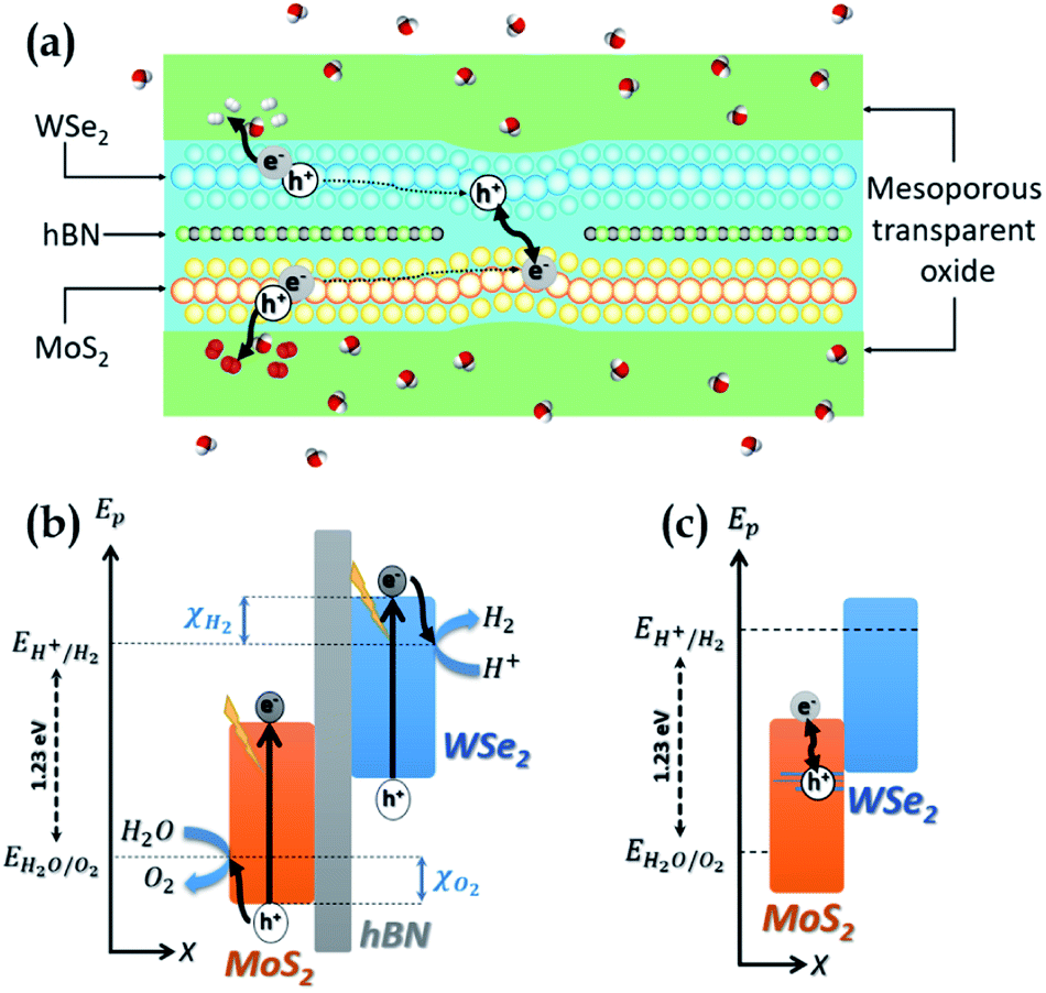 | ||
| Fig. 1 (a) Schematic representation of the SWS system. The active core is based on a MoS2/hBN/WSe2 vdWH and a MoS2/WSe2 vdWH. A transparent mesoporous oxide supports and protects the active core. (b) Sketch of the band diagram in the first region where the MoS2 and WSe2 are isolated by hBN. EH+/H2 and EH2O/O2 are respectively the reaction potentials of the reduction of H+ in H2 and of the oxidation of H2O and O2. This region is the seat of carrier generation and electrochemical reactions. (c) Sketch of the band diagram in the second region, without hBN. This region enables the recombination of the excess carriers. | ||
One must encapsulate the ultra-thin active core to protect and support it without avoinding the circulation of water and gases. To this end, mesoporous transparent oxides28 appear as good option. Also, high-quality optical absorption in the TMDCs is essential as their ultimate thinness remains limiting. Many works have been interested in improving optical absorption in 2D materials, as presented in the review by Li et al.29 The mesoporous oxides can serve as a support for absorption enhancement systems, such as photonic crystals, resonant cavities, nanoparticles.
3 Model
To estimate the realistic efficiency of our system, we have developed a detailed balance model based on ab initio calculations. The foundation of this model is inspired by the work of Fountaine et al.30 We first compute an inverse formulation of the current–voltage characteristic of a photoelectrochemical system, VPEC(J),| VPEC(J) = VMoS2(J) + VWSe2(J) − VMoS2/WSe2(−J) − Vcat,a/c(J) ≥ Erxn | (1) |
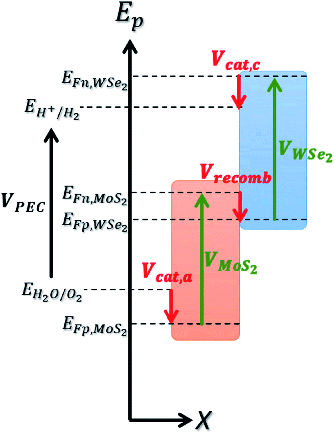 | ||
| Fig. 2 Representation of the different voltages involved in the computation of VPEC, depicted on the band diagram of the MoS2/WSe2 heterojunction. The green arrows represent the voltages generated by the devices. Red arrows represent the losses induced by catalytic overpotentials and carrier's recombination in the region without hBN. EFn and EFp represent the energy of the pseudo-Fermi level of electrons and holes respectively. | ||
The voltage VPEC must be greater than or equal to the electrochemical reaction potential for the reaction to take place. For water electrolysis, this potential is Erxn = 1.23 V.
We compute the current–voltage characteristics of the isolated MoS2, the isolated WSe2 and the MoS2/WSe2 heterojunction to calculate VMoS2(J) and VWSe2(J) and VMoS2/WSe2(J) respectively. To this end, we use a detailed balance model based on the balance between the generation and the recombination rates of the electron/hole pairs. The carrier generation rate GTMDC is the number of electron–hole pairs photogenerated in the TMDC per unit of volume and time. Here, “TMDC” refers to either MoS2, WSe2 or the MoS2/WSe2 heterojunction. GTMDC depends on the number of incident photons and the absorption of these photons. In this paper, we use the AM1.5 G solar spectrum. The generation rate is given by the expression
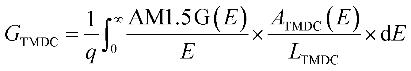 | (2) |
The absorbance ATMDC(E) is a function of the absorption coefficient of the materials and the geometry of the active core. We use DFT to compute the ab initio absorption coefficients of MoS2, WSe2 and the MoS2/WSe2 heterojunction. The complete expression of ATMDC(E) is presented in ESI 1.†
The carrier recombination rate RTMDC is the number of recombination of electron–hole pairs in each TMDC per unit of volume and time. We use generalized Planck's law to describe spontaneous radiative recombination. To take into account the non-radiative recombination, we introduce an external radiative efficiency coefficient (ERE)31 in the calculation of RTMDC. The latter is given by
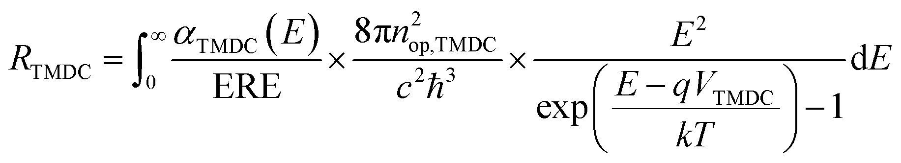 | (3) |
As the recombination rate RTMDC depends on VTMDC, we can define the current–voltage characteristic of a TMDC of thickness LTMDC as:
| J(VTMDC) = −q(GTMDC − RTMDC(VTMDC))LTMDC | (4) |
We now introduce the parameter γ which represents the fraction of the MoS2/hBN/WSe2 heterojunction in the active core. The proportion 1 − γ is thus the fraction of the region without hBN. In the region with the hBN, eqn (4) thus becomes
| J(VTMDC) = −q × γ(GTMDC − RTMDC(VTMDC))LTMDC | (5) |
| J(VHJ) = −q × (1 − γ)(GHJ − RHJ(VHJ))LHJ | (6) |
We numerically invert eqn (5) to get the relations VMoS2(J) and VWSe2(J), and we invert eqn (6) to get VMoS2/WSe2(J).
To determine the current dependence of the catalytic overpotentials we use an inverse formulation of the Butler–Volmer kinetics and we assume that the charge transfer coefficients at the anode and the cathode are equal (αa = αc = α).32 We implement the overpotentials of the anode and the cathode Vcat,a/c(J) with the following expression,
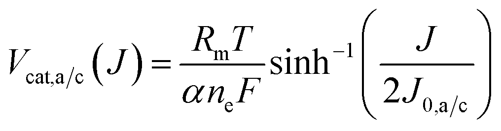 | (7) |
Once eqn (1) is implemented, we calculate the STH efficiency of the device. To do so, we first compute the optimal current density Jop, which is the maximum current density that satisfies the condition VPEC(Jop) ≥ 1.23 V. We get ηPEC, the STH efficiency, thanks to the following equation:
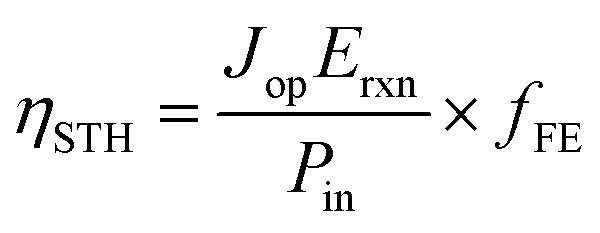 | (8) |
 | (9) |
Before presenting the results of the model, we focus on its important parameters. We classify them into two categories: intrinsic parameters and parameters related to the design of the device. The first category accounts for the non-ideality of the materials and their heterojunctions and includes the external radiative efficiency (ERE) and the anodic and cathodic catalytic exchange current density (J0,a and J0,c respectively). These intrinsic parameters are specific to the materials and their manufacture and a priori unknown for our system. Inspired by the work of Fountaine et al.,30 we distinguish three cases, summarised in Table 1, to study the STH efficiency of the device. Case no. 1 corresponds to the ideal limit case where each recombination is radiative (ERE = 1) and the overpotentials are zero (which corresponds mathematically to infinite catalytic exchange current densities). Case no. 2 is a realistic case with high radiative and electrochemical performances. Finally, case no. 3 accounts for average radiative and electrochemical quality. We assume that the external radiative efficiencies are equal for the isolated TMDCs and the heterojunction. We discuss the validity and the consequences of this assumption in ESI 2.†
| Case | ERE | J 0,a (mA cm−2) | J 0,c (mA cm−2) |
|---|---|---|---|
| No. 1 | 1 | +∞ | +∞ |
| No. 2 | 10−2 | 10−3 | 1 |
| No. 3 | 10−6 | 10−5 | 1 |
The second category of parameters groups two design parameters: γ, the proportion of region with hBN and N, the absorption quality. We introduced γ during the presentation of the model in eqn (5) and (6). N represents the number of light passages through the device. It models, in a simplified manner, the absorption quality, which can be enlarged by considering for instance a photonic crystal, a resonant cavity and/or by considering several layers of the active core. We describe the influence of N on the active core absorption in ESI 1.†
4 Results and discussion
In this section, we present the significant results in three steps. First, we show the ab initio results of band structures and absorption coefficients. We describe the computational methods used for these ab initio calculations in ESI 3.† Then we study the system efficiency versus the design parameters (γ and N) according to the three cases (ideal, high performance and standard quality). Finally, we emphasise the influence of the intrinsic parameters (ERE and J0,a/c) on the STH efficiency of the device.We first present the ab initio band structure calculated with DFT. The band structures of the isolated materials are shown in ESI 4† and are in good agreement with the literature. From these band structures, we deduce χO2 and χH2 from the redox potentials EH2O/O2 and EH+/H2 respectively. These redox potentials have a bearing on the pH of water and are calculated with the following expression,23
| EH2O/O2 = −4.44 eV + pH × 0.059 eV | (10) |
| EH+/H2 = −5.67 eV + pH × 0.059 eV | (11) |
Fig. 3 shows the projected band structure of the MoS2/WSe2 heterojunction. The red (blue) dots represent electronic states around the nuclei of MoS2 (WSe2). We first note that the band structure shows a direct band gap of 0.58 eV at the K point of the first Brillouin zone. We identify the band edge electronic states mainly localised around MoS2 or WSe2 and thus find a type II (tandem) heterojunction. The band structure shows that the band gap of the MoS2 is 1.46 eV and that of the WSe2 is 1.88 eV. We note that these values are different from the gaps obtained for the isolated materials (ESI 4†) due to the stress induced by the heterojunction.33 Finally, the most important point to note in this band structure is the state hybridisation in the valence band. Close to the VBM, the electronic states are localised around both MoS2 and WSe2. This hybridisation enables direct recombination of electrons and holes in MoS2. Hence, we expect radiative recombination with emission of photons of energy Eg = 0.58 eV. This hybridization is confirmed by experimental results which show the existence of an interlayer exciton in this heterojunction.27 Regarding both the band alignment and the type II configuration, the MoS2/WSe2 heterojunction fulfils the basic requirements of the overall water splitting.
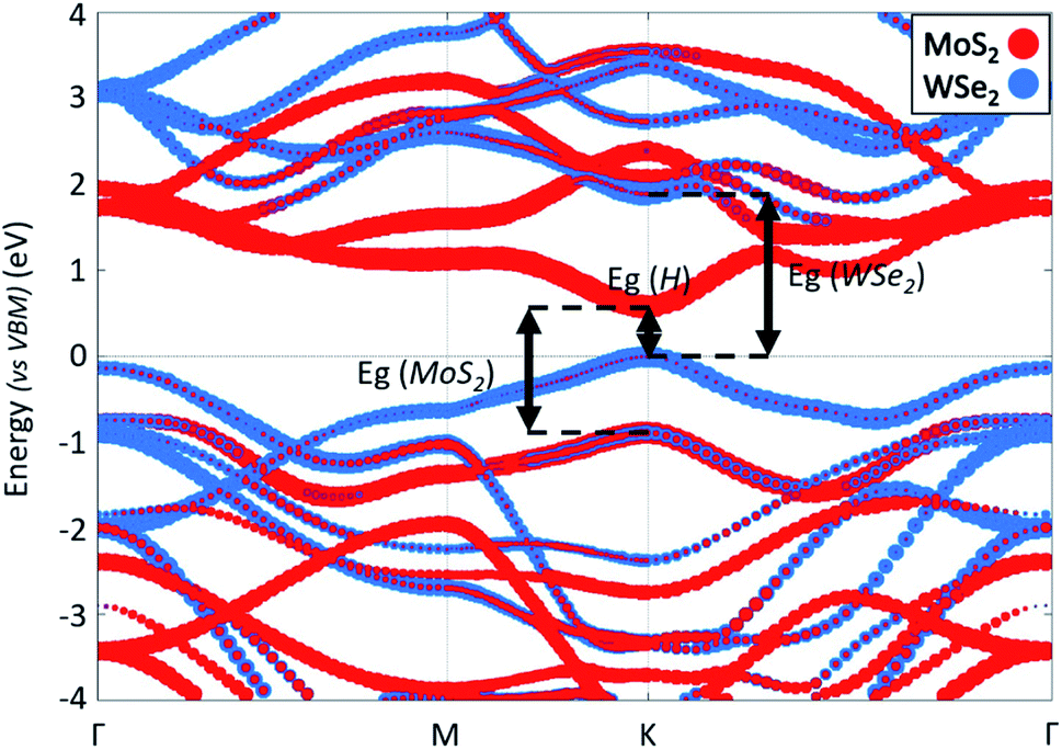 | ||
| Fig. 3 Band structure of the MoS2/WSe2 heterojunction along a Γ–M–K–Γ path. The energy reference is set to VBM. The red (blue) dots represent electronic states around the nuclei of MoS2 (WSe2). | ||
Fig. 4 displays the ab initio absorption coefficients of the isolated MoS2 and WSe2 and their heterojunction. The absorption coefficient of the isolated monolayers, Fig. 4(a), shows that MoS2 and WSe2 have analogous behaviours around the band edges. This could be a problem in the case of a 3D heterojunction where the top material would absorb all the incident light. Due to their extreme thinness, the single-pass absorption of 2D TMDCs is less than 10%.34 In a 2D vdWH, the top TMDC will absorb less than 10% of the incident light. The remaining more than 90% will be available for the bottom TMDC, which will in turn absorb 10%. Having two absorbers in the same energy range is therefore not a problem for the operation of the device. However, we will see below that we must enhance the total absorption to improve the efficiency of the system, i.e. we need more than a single-pass. Fig. 4(b), which represents the absorption coefficient of the MoS2/WSe2 heterojunction, shows that the absorption is non-zero for energy larger than 0.4 eV. Corresponding radiative recombination is thus expected.
 | ||
| Fig. 4 (a) Absorption coefficient of MoS2 (red curve) and WSe2 (blue curve) versus the photon energy. (b) Absorption coefficient of the MoS2/WSe2 heterojunction. In both graphs, the inset plot is a zoom in the low energy range. | ||
Using these absorption coefficients and our multiphysics model, we calculate the system efficiency. Fig. 5 presents the STH efficiency ηSTH according to the design parameters for the three cases previously described in Table 1. Fig. 5(a) shows a strong dependence of the efficiency with N. Without optical absorption enhancement (i.e. N = 1), the STH efficiency is less than 0.5% whatever the case. Hence, the development of high-performance absorption enhancement system is mandatory to get valuable efficiencies. At high absorption quality (N > 1000), the efficiency saturates because all the photons are absorbed. The efficiency is 17.2% in cases no. 1 and no. 2 and 13.8% in case no. 3. The absorption quality is then a key factor in the device performance. Indeed, for a constant incident power, better absorption generate more carriers and thus a larger current, which increases the STH efficiency (eqn (8)). Even if the parameter N is a simplified way of describing the absorption, we use it to state that to reach 10% efficiency in case no. 3, the active core must absorb 71% of the photons with an energy higher than the band gap energy. In case no. 2, it has to absorb 56% of the incident light in the same energy range to reach the 10% efficiency. We present the detail of these statements in ESI 5.†
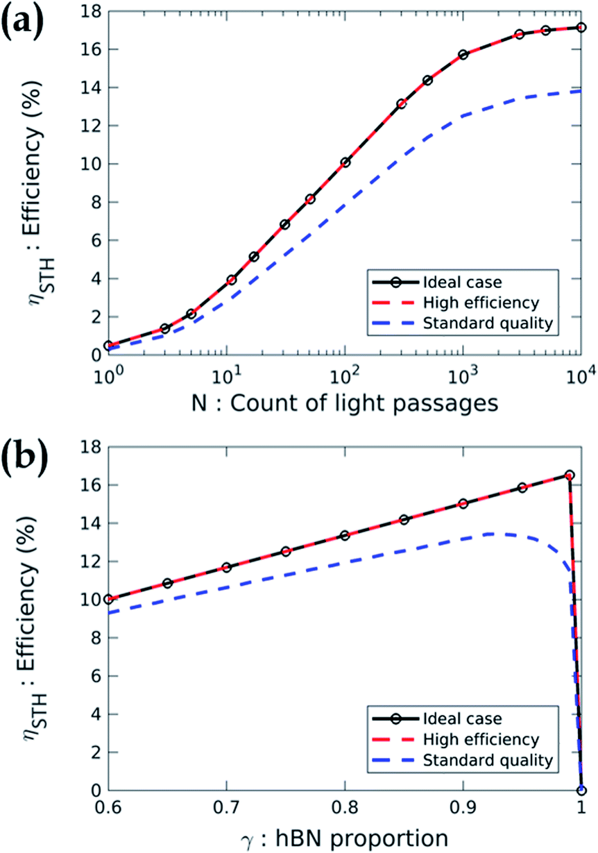 | ||
| Fig. 5 (a) STH efficiency versus N, the absorption quality, according to three cases (ideal materials, high-efficiency materials and standard quality materials). γ is set to 0.99 for ideal and high efficiency materials and set to 0.93 for standard quality materials (b) STH efficiency versus γ, the proportion of region with hBN, according to the same cases. Here, N is set to 3001 for each case. | ||
Fig. 5(b) depicts the STH efficiency versus the proportion of region with hBN. The result shows that γ must be larger than 0.9 whatever the case. Indeed, increasing the proportion of the MoS2/hBN/WSe2 heterojunction increases the surface of the device dedicated to photon absorption and electrochemical reactions. Moreover, the recombination in the region without hBN is sufficiently efficient to be non-limiting. However, if γ is too close to 1, the efficiency drops to zero because there is not enough recombination of the excess carriers. This result is advantageous for the design of the device since one can imagine to randomly stack exfoliated flakes of MoS2 then hBN and finally, WSe2 to produce the active core. This non-ideal stacking will inevitably create some regions without hBN which will naturally enable the recombination of the carriers.
In both graphs of Fig. 5(a) and (b), we note that the curves representing cases no. 1 and no. 2 (i.e. the ideal case and the case of high-performance materials) are identical. To understand this result, we study the STH efficiency versus the intrinsic parameters. Fig. 6 shows ηSTHversus the external radiative efficiency ERE and versus the catalytic exchange current density at the anode j0,c.‡ The efficiency is zero if the intrinsic parameters are too poor. Indeed, poor radiative efficiency (i.e. ERE ≪ 1) leads to a low voltage generated by TMDCs and a poor catalytic behaviour (i.e. weak j0,a/c) requires applying a larger overpotential to maintain a given current density. We refer the reader to ESI 6 and 7† for more details on the influence of radiative efficiency and the exchange current density respectively. The combination of these two phenomena leads to a voltage available for the electrochemical reaction too low to enable the electrolysis of water (we have VPEC(J) < 1.23 V regardless of the current density), which gives a zero efficiency. This is the case for example if ERE = 10−7 and J0,a = 10−8 mA cm−2 where the maximum voltage that the system can deliver is 1.16 V. Conversely, beyond a certain quality of the materials, better intrinsic parameters do not improve the performance. The latter presents constant 16.4% efficiency (Fig. 6) which is reached when the following condition is observed: Jop = min(JSC,MoS2; JSC,WSe2) where JSC,MoS2 and JSC,WSe2 are the short-circuit current densities of MoS2 and of WSe2 respectively. Once the efficiency reaches this limit, it is no longer useful to increase the voltages delivered by the cells or to decrease the losses.
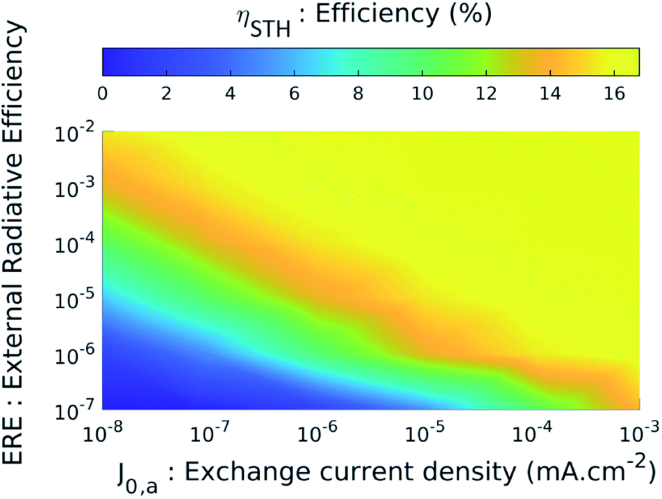 | ||
| Fig. 6 STH efficiency versus two intrinsic parameters, the external radiative efficiency ERE and the anodic exchange current density J0,a. Here, N is set to 3001 and γ is set to maximise the efficiency for each point (γ lies between 0.82 and 0.99). J0,c is set according to case 2 (i.e. J0,c = 1 mA cm−2). | ||
5 Conclusions and perspectives
In conclusion, we propose in this article a vdWH for overall water splitting. The bias is produced by MoS2 and WSe2 monolayers in a direct Z-scheme vdWH. The system is unassisted and is based on non-toxic, earth abundant materials. The photoelectrochemical model, based on ab initio results, shows a STH efficiency of more than 10% for standard photovoltaic and electrochemical quality materials. Since TMDCs are very promising for these applications, we can expect efficiencies over 15%. This efficiency exceeds the critical 10% efficiency required to make SWS economically viable.20,35 The system requires simple manufacturing processes (exfoliation), which enables production of carbon-free hydrogen without using rare metals. This system can also be considered for decentralised production, which can be advantageous in remote places or for individual uses.It is, however, important to note that the DFT calculations involve systematic errors, in particular in the computation of the band gap energies of the system.36 These numerical results will have to be compared with experimental results of the optical properties of the 2D TMDCs (isolated and in heterojunction). These measurements will be the subject of future work. If the DFT calculations have underestimated the band gap energies too much, it will be possible to adjust the model with the new values. It is also conceivable to consider other TMDCs exhibiting photoelectrochemical properties similar to or better than those of this paper. We also note that in our study, the calculated band gaps of MoS2 and WSe2 are almost identical. This is not a necessary condition for the correct operation of the device. After selecting the active materials, it will be possible to carry out more in-depth and realistic modelling of the light management system. This point is crucial since the absorption quality is essential to obtain significant STH efficiency.
Conflicts of interest
There are no conflicts to declare.Acknowledgements
The authors acknowledge the Centre de Calcul Intensif d'Aix-Marseille for granting access to its high-performance computing resources.Notes and references
- R. Li and C. Li, Advances in Catalysis, Elsevier, 2017, vol. 60, pp. 1–57 Search PubMed.
- M. G. Walter, E. L. Warren, J. R. McKone, S. W. Boettcher, Q. Mi, E. A. Santori and N. S. Lewis, Chem. Rev., 2010, 110, 6446–6473 CrossRef CAS PubMed.
- Q. Xu, L. Zhang, J. Yu, S. Wageh, A. A. Al-Ghamdi and M. Jaroniec, Mater. Today, 2018, 21, 1042–1063 CrossRef CAS.
- T. Hisatomi, J. Kubota and K. Domen, Chem. Soc. Rev., 2014, 43, 7520–7535 RSC.
- Q. Wang and K. Domen, Chem. Rev., 2020, 120, 919–985 CrossRef CAS PubMed.
- J. Abdul Nasir, A. Munir, N. Ahmad, T. ul Haq, Z. Khan and Z. Rehman, Adv. Mater., 2021, 33, 2105195 CrossRef CAS PubMed.
- S. Das, D. Pandey, J. Thomas and T. Roy, Adv. Mater., 2019, 31, 1802722 CrossRef PubMed.
- M. Amani, D.-H. Lien, D. Kiriya, J. Xiao, A. Azcatl, J. Noh, S. R. Madhvapathy, R. Addou, S. Kc, M. Dubey, K. Cho, R. M. Wallace, S.-C. Lee, J.-H. He, J. W. Ager, X. Zhang, E. Yablonovitch and A. Javey, Science, 2015, 350, 1065–1068 CrossRef CAS PubMed.
- N. Ansari and E. Mohebbi, Opt. Mater., 2016, 62, 152–158 CrossRef CAS.
- C. Janisch, H. Song, C. Zhou, Z. Lin, A. L. Elías, D. Ji, M. Terrones, Q. Gan and Z. Liu, 2D Mater., 2016, 3, 025017 CrossRef.
- D. Jariwala, A. R. Davoyan, J. Wong and H. A. Atwater, ACS Photonics, 2017, 4, 2962–2970 CrossRef CAS.
- Y. Li, A. Chernikov, X. Zhang, A. Rigosi, H. M. Hill, A. M. van der Zande, D. A. Chenet, E.-M. Shih, J. Hone and T. F. Heinz, Phys. Rev. B: Condens. Matter Mater. Phys., 2014, 90, 205422 CrossRef.
- N. Cavassilas, D. Logoteta, Y. Lee, F. Michelini, M. Lannoo, M. Bescond and M. Luisier, J. Phys. Chem. C, 2018, 122, 28545–28549 CrossRef CAS.
- T. Roy, M. Tosun, X. Cao, H. Fang, D.-H. Lien, P. Zhao, Y.-Z. Chen, Y.-L. Chueh, J. Guo and A. Javey, ACS Nano, 2015, 9, 2071–2079 CrossRef CAS PubMed.
- N. Oliva, J. Backman, L. Capua, M. Cavalieri, M. Luisier and A. M. Ionescu, npj 2D Mater. Appl., 2020, 4, 1–8 CrossRef.
- Z. Zhou, X. Niu, Y. Zhang and J. Wang, J. Mater. Chem. A, 2019, 7, 21835–21842 RSC.
- K. Si, J. Ma, C. Lu, Y. Zhou, C. He, D. Yang, X. Wang and X. Xu, Appl. Surf. Sci., 2020, 507, 145082 CrossRef CAS.
- J. Wu, M. Liu, K. Chatterjee, K. P. Hackenberg, J. Shen, X. Zou, Y. Yan, J. Gu, Y. Yang, J. Lou and P. M. Ajayan, Adv. Mater. Interfaces, 2016, 3, 1500669 CrossRef.
- X. Yin, C. S. Tang, Y. Zheng, J. Gao, J. Wu, H. Zhang, M. Chhowalla, W. Chen and A. T. S. Wee, Chem. Soc. Rev., 2021, 50, 10087–10115 RSC.
- Y. Fan, J. Wang and M. Zhao, Nanoscale, 2019, 11, 14836–14843 RSC.
- J. Shen, Y. He, J. Wu, C. Gao, K. Keyshar, X. Zhang, Y. Yang, M. Ye, R. Vajtai, J. Lou and P. M. Ajayan, Nano Lett., 2015, 15, 5449–5454 CrossRef CAS PubMed.
- M. M. Bernal, L. Álvarez, E. Giovanelli, A. Arnáiz, L. Ruiz-González, S. Casado, D. Granados, A. M. Pizarro, A. Castellanos-Gomez and E. M. Pérez, 2D Mater., 2016, 3, 035014 CrossRef.
- M. Cao, L. Ni, Z. Wang, J. Liu, Y. Tian, Y. Zhang, X. Wei, T. Guo, J. Fan and L. Duan, Appl. Surf. Sci., 2021, 551, 149364 CrossRef CAS.
- D. Wickramaratne, L. Weston and C. G. Van de Walle, J. Phys. Chem. C, 2018, 122, 25524–25529 CrossRef CAS.
- A. Rousseau, L. Ren, A. Durand, P. Valvin, B. Gil, K. Watanabe, T. Taniguchi, B. Urbaszek, X. Marie, C. Robert and G. Cassabois, Nano Lett., 2021, 21, 10133–10138 CrossRef CAS PubMed.
- S. Latini, K. T. Winther, T. Olsen and K. S. Thygesen, Nano Lett., 2017, 17, 938–945 CrossRef CAS PubMed.
- O. Karni, E. Barré, S. C. Lau, R. Gillen, E. Y. Ma, B. Kim, K. Watanabe, T. Taniguchi, J. Maultzsch, K. Barmak, R. H. Page and T. F. Heinz, Phys. Rev. Lett., 2019, 123, 247402 CrossRef CAS PubMed.
- N. Sharma, H. Ma, T. Bottein, M. Bugnet, F. Vocanson, D. Grosso, T. E. Itina, Y. Ouerdane and N. Destouches, J. Phys. Chem. C, 2019, 123, 6070–6079 CrossRef CAS.
- Q. Li, J. Lu, P. Gupta and M. Qiu, Adv. Opt. Mater., 2019, 7, 1900595 CrossRef CAS.
- K. T. Fountaine, H. J. Lewerenz and H. A. Atwater, Nat. Commun., 2016, 7, 13706 CrossRef CAS PubMed.
- M. A. Green, Prog. Photovoltaics, 2012, 20, 472–476 CAS.
- K. T. Fountaine, H. J. Lewerenz and H. A. Atwater, Appl. Phys. Lett., 2014, 105, 173901 CrossRef.
- H. J. Conley, B. Wang, J. I. Ziegler, R. F. Haglund, S. T. Pantelides and K. I. Bolotin, Nano Lett., 2013, 13, 3626–3630 CrossRef CAS PubMed.
- M. Bernardi, M. Palummo and J. C. Grossman, Nano Lett., 2013, 13, 3664–3670 CrossRef CAS PubMed.
- B. A. Pinaud, J. D. Benck, L. C. Seitz, A. J. Forman, Z. Chen, T. G. Deutsch, B. D. James, K. N. Baum, G. N. Baum, S. Ardo, H. Wang, E. Miller and T. F. Jaramillo, Energy Environ. Sci., 2013, 6, 1983 RSC.
- M. Grüning, A. Marini and A. Rubio, J. Chem. Phys., 2006, 124, 154108 CrossRef PubMed.
Footnotes |
| † Electronic supplementary information (ESI) available: Absorbance formula, justification of the external radiative efficiency hypothesis, ab initio methods, TMDC band structures, modelling of the absorption enhancement system, influence of the intrinsic parameters. See https://doi.org/10.1039/d2na00178k |
| ‡ The cathodic exchange current density difference between standard and high-quality materials is negligible. It is not the case of the anodic exchange current density. |
| This journal is © The Royal Society of Chemistry 2022 |