
 Open Access Article
 This Open Access Article is licensed under a Creative Commons Attribution-Non Commercial 3.0 Unported Licence
Rotaxane nanomachines in future molecular electronics
Peiqiao
Wu
a,
Bhushan
Dharmadhikari
 d,
Prabir
Patra
*b and
Xingguo
Xiong
*c
d,
Prabir
Patra
*b and
Xingguo
Xiong
*c
aDepartment of Computer Science and Computer Engineering, University of Bridgeport, Bridgeport, CT, USA. E-mail: peiqiaow@my.bridgeport.edu
bDepartment of Biomedical Engineering and Mechanical Engineering, University of Bridgeport, Bridgeport, CT, USA. E-mail: ppatra@bridgeport.edu
cDepartment of Electrical Engineering and Computer Engineering, University of Bridgeport, Bridgeport, CT, USA. E-mail: xxiong@bridgeport.edu
dDepartment of Electrical and Computer Engineering and Technology, Minnesota State University, Mankato, MN, USA. E-mail: bhushan.dharmadhikari@mnsu.edu
First published on 24th June 2022
Abstract
As the electronics industry is integrating more and more new molecules to utilize them in logic circuits and memories to achieve ultra-high efficiency and device density, many organic structures emerged as promising candidates either in conjunction with or as an alternative to conventional semiconducting materials such as but not limited to silicon. Owing to rotaxane's mechanically interlocked molecular structure consisting of a dumbbell-shaped molecule threaded through a macrocycle, they could be excellent nanomachines in molecular switches and memory applications. As a nanomachine, the macrocycle of rotaxane can move reversibly between two stations along its axis under external stimuli, resulting in two stable molecular configurations known as “ON” and “OFF” states of the controllable switch with distinct resistance. There are excellent reports on rotaxane's structure, properties, and function relationship and its application to molecular electronics (Ogino, et al., 1984; Wu, et al., 1991; Bissell, et al., 1994; Collier, et al., 1999; Pease, et al., 2001; Chen, et al., 2003; Green, et al., 2007; Jia, et al., 2016). This comprehensive review summarizes [2]rotaxane and its application to molecular electronics. This review sorts the major research work into a multi-level pyramid structure and presents the challenges of [2]rotaxane's application to molecular electronics at three levels in developing molecular circuits and systems. First, we investigate [2]rotaxane's electrical characteristics with different driving methods and discuss the design considerations and roles based on voltage-driven [2]rotaxane switches that promise the best performance and compatibility with existing solid-state circuits. Second, we examine the solutions for integrating [2]rotaxane molecules into circuits and the limitations learned from these devices keep [2]rotaxane active as a molecular switch. Finally, applying a sandwiched crossbar structure and architecture to [2]rotaxane circuits reduces the fabrication difficulty and extends the possibility of reprogrammable [2]rotaxane arrays, especially at a system level, which eventually promotes the further realization of [2]rotaxane circuits.
1 Introduction
In 1965, Gordon Moore, Fairchild Semiconductor's Director of R&D, made a famous prediction that the number of transistors per silicon chip would double every 1–2 years. Ever since then, the “Moore's law” has governed the VLSI (Very Large-Scale Integration) industry fairly well for many decades. VLSI technology has been driven by rapid performance improvement and constant integration scale growth. A modern VLSI chip could contain billions of transistors, with a minimum feature size of 10 nm and below.1–3 These are all based on the miniaturization of transistor size in the fabrication process. The smaller the transistor size is, the more transistors can be put into the same chip area. A smaller size, higher speed, and lower energy consumption are the constant trends driving the rapid growth of VLSI technology generation after generation. However, nowadays Moore's law is approaching the physical limits of the manufacturing process. The current minimum gate width of a transistor is already less than 10 nm. If the size continues to shrink down, the manufacturing process will become inordinately difficult. First, the transistor with extremely narrow gate size demonstrates a sharp decline in its current-control ability, resulting in “leakage current”.4–6 Besides, in order to integrate more transistors on the chip, the silicon dioxide insulating layer has to be thinner and thinner, which also results in leakage current. Eventually, the leakage current causes extra power consumption, as well as signal degradation and error in the circuit. Second, when manufacturing the chip at 5 nm and below, the electrons of the transistor will experience the quantum tunneling effect, and they will no longer move along the established route.5,7–9 As a result, the characteristics of the transistor will be out of control, and the difficulty and capital cost of semiconductor fabrication will increase exponentially. The question, whether Moore's law will fail in the future, has become the Damocles sword hanging over the head of the silicon-based semiconductor industry. In order to overcome the above challenges and continue to extend Moore's Law, disruptive innovation and technology breakthroughs are imminent and in pressing need. With the rapid emergence of nanotechnology, it offers a promising opportunity for the VLSI industry to make transition from the “microelectronics” into the “nanoelectronics” paradigm. What is the technology beyond silicon microelectronics? Many potential candidates are available, including but not limited to single-electron transistors (SETs),10–12 quantum computing,13,14 quantum-dot cellular automata (QCA), carbon-nanotube-based transistors,15–19 nanowire crossbar architecture,20–22 CMOL (CMOS-molecular circuits),23,24 rotaxane/catenane-based moletronics (molecular electronics), etc. Researchers are making efforts to explore all the potential technology candidates. This is like a fair race of all the choices, and the final winner will shape the future of nanoelectronics and carry the hope to continue Moore's law to sustain the continuing growth of the VLSI industry. Among them, rotaxane-based molecular electronics is a very attractive solution due to its high device density, low energy consumption and high efficiency. A rotaxane is a mechanically interlocked molecular structure consisting of a dumbbell shaped molecule threaded through a macrocycle. It demonstrates to be able to switch between two stable states: one with high resistance (OFF state) and one with low resistance (ON state). Such switching is reversible, controllable and repeatable. This makes it a perfect candidate to replace transistor switches in digital VLSI circuits. Based on this, it can be used for digital memory and/or logic gate applications. Furthermore, it can be used to construct a nanowire cross-bar architecture (rows and columns) with rotaxane switches in each cross junction of the nanowires. Such an array structure is a promising choice due to its reconfigurability, programmability, and fault-tolerance. It can be easily formed into a Field Programmable Gate Array (FPGA) architecture, so that users can program its structure into different connections for digital memory and logic gates. The cost of molecular materials is low, and the circuit elements can be synthesized chemically in mass productions. Moletronics has the advantages of extremely high device density, low power consumption, and high efficiency and the feature size is automatically reduced to the molecular scale.2 Moletronics
What is molecular electronics, or “moletronics”? According to the name, moletronics uses molecules for electronic applications. That is, it directly uses individual molecules as building blocks to function as electronic components, assemble them into electronic circuits, or even construct a complete computer system. It is an interdisciplinary field based on physics, chemistry, materials science, electrical engineering, computer engineering, and biology. Moletronics has the advantages of small size, low cost, low energy consumption and high efficiency. The idea of micro- and nanotechnology can be traced back to Richard Feynman's famous talk in 1959 – “There's Plenty of Room at the Bottom”.25 In that talk, he made a prediction that as the technology advanced, there will be tremendous opportunities in the small-size world, where scientists could manufacture extremely small-size devices and components for different applications. As an example, he predicted that the diameter of the wire can be as small as 10–100 atoms, and the circuit can be as small as several thousand angstroms. He also predicted that it was possible in future that physical laws allow the use of atoms to create small objects. Many of his predictions have already come true, and some of them are still waiting for scientists to implement in the future. His unique vision led to a very important direction – technology trends tend to become smaller and smaller, and there are plenty of exciting opportunities in research, invention and applications of the “small” world. It was not easy for him to have this bold idea and vision about “small” research at that time, but time proved that his prediction was very true. VLSI technology, the foundation of modern computers and internet, was exactly driven by the miniaturization of transistor size, from microns to nanometers. In this way, millions and billions of transistors can be connected together into VLSI circuits with different functionalities for different applications. Micro- and nanotechnology have also shrunk the size of sensors, actuators to be integrated into System-on-Chip (SoC). For nanoelectronics applications, a digital counterpart device – molecular switch – is needed. Such a molecular switch should demonstrate two stable states with high and low resistances, which could be an excellent candidate for molecular electronic circuits. Research work about various molecules demonstrating digital switching behavior has been reported.26–31 Among them, [2]rotaxane is a very promising candidate to replace silicon transistors for future moletronics applications. Furthermore, many types of molecular components other than molecular switches have also been reported, including molecular transistors,16,17,32–34 molecular diodes,35–39 molecular capacitors,40,41 molecular insulators,42etc. Individual molecules may have totally different properties as bulk materials. A thorough understanding about the behavior and working principle of these molecules is required before they can be used for moletronics applications. At the molecular level, traditional physics laws may not be applicable and quantum mechanics must be used. It is necessary to analyze phenomena with quantum theory and to study electronic behavior and thermodynamics at the molecular level. In this paper, we will propose three levels of challenges that need to be solved in molecular electronics. Focusing on these three major challenges, we reveal what progress has been made in molecular electronics, and what relationship between molecular electronics and silicon-based circuits should be in the future. Finally, with respect of the three major challenges of moletronics, we explain how rotaxane could help to find a solution. Rotaxane as a molecular switch could play a significant role leading to the future success of molecular electronics.Compared to silicon-based semiconductors, the main advantages of molecular electronics are small size, high speed, low cost, and new characteristics.43–46 The size of a single molecule is as small as about a few nanometers. It was previously considered to be the greatest advantage of molecular electronics. However, with the constant effort in the VLSI industry to push the limit, nowadays the feature size of silicon-based technology has been shrunk to deep submicron and nanometer levels. For example, Samsung's latest gate-all-around field-effect transistor has a process feature size below 5 nm.47,48 Thus, the size of traditional top-down fabricated microelectronics is already comparable to that of molecular electronics. However, moletronics offers opportunities which may not be possible in traditional microelectronics. For example, the molecules used for moletronics generally have high diversity in their molecular structure and properties, leading to a wide variety of choices and opportunities for different applications. Taking [n]rotaxane as an example, it is a family with many different species. They have different spatial geometric structures, isomers and chemical groups with different characteristics. These natural molecules or artificially synthesized supramolecular nanomaterials may exhibit different electronic characteristics. Some of them exhibit new features that do not exist in traditional solid-state devices. Moreover, moletronics generally operates under the law of quantum mechanics. A lot of new phenomena such as quantum parallelism, quantum entanglement, and quantum tunneling come inherently in quantum physics. This would enable many extraordinary functions which we have never seen before with traditional microelectronics. It could bring about revolutionary changes to VLSI technology. Furthermore, molecular electronics may enable “stacking” of multiple planar transistor layers into 3D (3-dimension) electronics which could further significantly increase the current device density level. This is because the energy consumption of individual molecule is much less. Some nanomaterials (e.g., nanotube) show superior thermal conductivity which could help solve the heat dissipation problem of 3D moletronics. Instead, current silicon-based VLSI remains 2-dimensional architecture due to the bottleneck of heat dissipation and 3-dimensional packaging challenges. Last, moletronics also benefits from its low cost of materials and fabrication. Each individual molecule functions as an electronic component, and this leads to ultimate efficiency in material usage. Molecules can be obtained through large-scale chemical synthesis. The characteristics of molecules can be easily modified through a specific chemical synthesis process. Molecular interactions can be used to form specific molecular layers through a bottom-up self-assembly process.49–51
On the other hand, moletronics also has its own limitations. For example, molecules generally show thermal instability at high temperatures. The control and operation of moletronics at the molecular level follow quantum mechanics, making it more complicated than traditional microelectronics. At this time, moletronics is still in its infancy stage. However, the potential impact and benefits moletronics could bring to microelectronics are tremendous and beyond imagination. Given some time, it could result in a revolutionary change and improvement in the current VLSI industry.
3 On-going work of [2]rotaxane and its applications to moletronics
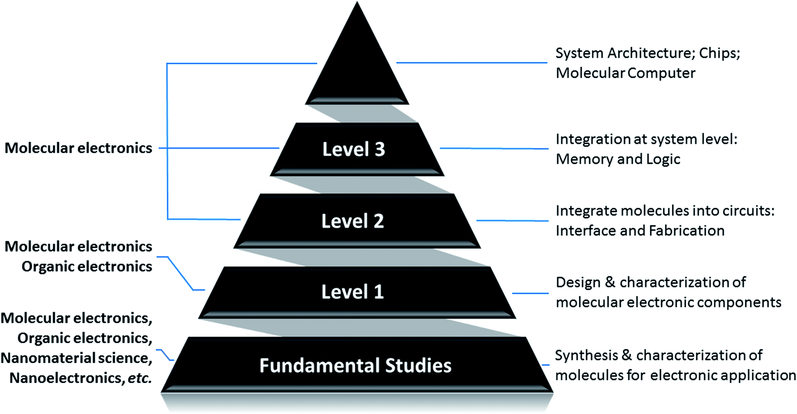
The entire modern VLSI is based on the basic building blocks – CMOS (Complementary Metal–Oxide–Semiconductor) transistors. Transistors, or CMOS transistors, are eventually implementing switching function between “OFF” and “ON” states. This allows them to represent binary data (digital “0” and “1”) to achieve expected functionalities. To shift from microelectronics to nanoelectronics, or moletronics, we need to find the perfect candidate for the fundamental building block – a switch. Scientists found that [2]rotaxane demonstrates such attractive properties. It is bi-stable and can switch between two stable states with distinguishable high and low resistance in a controllable way. Furthermore, such transition is reversible, stable, and repeatable. This makes it a promising candidate for digital memory and logic gate applications in moletronics. Many research studies about [2]rotaxane and its applications to moletronics have been reported.52–166To summarize the on-going research studies about [2]rotaxane and its applications to molecular electronics, we sort the reported studies into a pyramid structure, as shown in Fig. 1. The pyramid describes the research of molecular electronics in a bottom-up approach. As the foundation of the pyramid, level 1 research is the design, synthesis, characterization and application of nanoscale molecular electronic components. It focuses on the individual molecule and attempts to have a thorough understanding about the behavior, mechanism and properties of the molecule. In level 2 research, the work aims at figuring out an appropriate interface between molecules and the connecting electrodes. Then in level 3 research, multiple molecular components can be connected together into a functional moletronic circuit. Finally, the top of the pyramid, which is the ultimate goal of the research, is to build a complete molecular computer or System-on-Chip (SoC). In short, below are the 3 levels of challenges which need to be thoroughly investigated in order to achieve the ultimate goal of molecular electronics:
 | ||
| Fig. 1 Sorting of research work in moletronics as a pyramid structure. | ||
Level 1: investigation of the characteristics of molecules to be used as molecular electronic components.
Level 2: integration of molecules into circuits: interface and fabrication.
Level 3: integration at the system level: memory and logic.
Up to now, the majority of the existing research work focused on the level 1 problem, which involves organic chemistry and molecular synthesis. Level 1 work emphasizes the study and verification of the properties of the molecule itself for potential molecular circuits. Research work at level 2 and level 3 is also being actively conducted and promising progress has been reported. Some researchers also proposed potential architecture design for complete molecular electronics-based systems and their integration/communication with traditional silicon microelectronics. Some research work may focus on one level of the problem, while simultaneously addressing other levels of the challenges as well. All these active research studies contribute toward shaping the paradigm of future molecular electronics.
3.1 Finding the molecular switch
Scientists have always been good at revealing the magic of natural biological macromolecular machines. One step further, scientists also explore the feasibility of lab-made, artificial molecules to design and develop nano-machines. In the 1980s, Jean-Pierre Sauvage connected two macrocycles together to form a mechanically interlocked molecular chain. This new molecular structure is named “Catenane”.167 Two interlocked macrocycles can move relatively to each other, which made it a prototype of the first artificial molecular machine. In the 1990s, Fraser Stoddart brought up an innovative interlocked molecular system called a rotaxane. He threaded a macrocycle onto a dumbbell shaft with two large ends and demonstrated that the molecular macrocycle was able to move along the dumbbell chain.168 Based on rotaxane, he designed and developed molecular machines such as molecular elevators and molecular muscles.169–171 In 1999, Bernard Feilinga became the first person to develop a molecular motor and build a molecular “car” based on it. Because of the outstanding contributions of the above three scientists in the field of molecular machine research, they jointly won the 2016 Nobel Prize in Chemistry.In 1974, Arieh Aviram and Mark Ratner published “Molecular Rectifiers”.172 This paper is considered the pioneering work of molecular electronics. For the first time, it expounded systematically a rectifying effect of the molecule with tetrathiafulvalene (TTF) in theory. Therefore, it can be used as a potential molecular rectifier in circuits. Later, more research proved the theoretical and practical feasibility of using molecules as electronic components. In order for molecular electronics applications, a bistable molecular switch with two states, preferably with a distinguishable resistance difference, is needed. In this way, it can represent the “0” and “1” states for digital information. Such a molecular switch should be able to be activated with certain external stimuli to transit between “OPEN” and “CLOSE” states reversibly. Based on this, a complete digital circuit architecture can be constructed. Among numerous candidates for molecular switches, [2]rotaxane turns out to be the most promising one.
Rotaxane is not a natural structure, instead, it is an artificially synthesized interlocking mechanical structure. It is a unique collection of supramolecules composed of one (or more) macrocycle interlocked to one (or more) chain molecule. The chain molecule is used as the shaft passing through the ring molecules, and two larger molecules are attached to both ends as “stoppers” for preventing the ring molecules from slipping out. This forms a stable interlocking supramolecular structure with mechanical bonds. The name “rotaxane” comes from Latin words, “rota” for wheel and “axis” for “axle”. The two components of a rotaxane are kinetically trapped. Since the ends of the dumbbell (or stoppers) are larger than the internal diameter of the ring, this ensures that the two components cannot be easily separated. Rotaxane is a large family, and the type can be determined according to the number of chains and rings. The general notation is [n]rotaxane (n = 2, 3, 4, 5, etc.), where n is the number of rotaxane components. Thus [2]rotaxane means it has exactly 2 molecular components: one ring and one axis. Compared to other rotaxanes, [2]rotaxane has simpler structure. Furthermore, it demonstrates bistable states with distinguishable resistance (high and low) and can make reversible switches between the two states. This makes it well suited for molecular electronics applications.
3.2 [2]Rotaxane – a bistable molecular switch
[2]Rotaxane is a bistable rotaxane that has two constitutional isomers with two recognition stations. According to the naming rules, “[2]” means that there are 2 components: one macrocycle and one chain molecule in the rotaxane structure. The macrocycle can shuttle freely between two stations under certain conditions. As a molecular switch, its basic working principle is to change the thermodynamic state of the molecule through external stimuli (e.g. voltage, light, chemicals and temperature change). Then, the molecule spontaneously falls to the lowest energy conformer, that is, the macrocycle moves from one station to another. Correspondingly, in the macrocycle switching process, in addition to the change in molecular conformation, the properties of the molecule, such as electrical or optical properties, change accordingly. The changes in the properties of the molecule mark two different output states with distinct resistances: one has low resistance and the other has high resistance. The switching process is reversible. From a circuit perspective, this makes [2]rotaxane a perfect switch for digital circuits: one represents the “ON” state (or digital “1”) and the other represents the “OFF” state (digital “0”) in Fig. 2. Based on this, it can be used for molecular memory and molecular logic applications.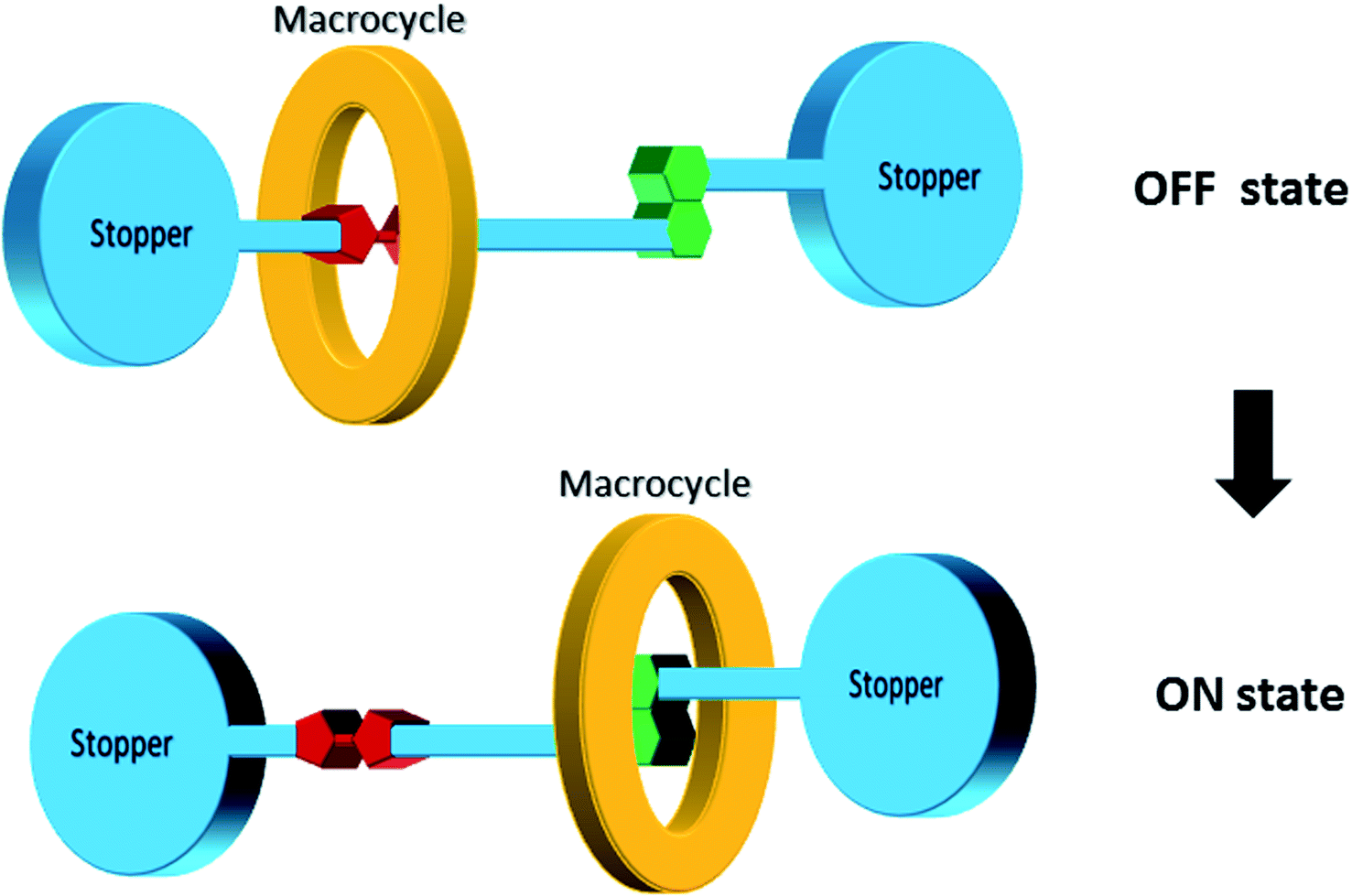 | ||
| Fig. 2 A schematic model of the [2]rotaxane switch. | ||
Fig. 2 describes the complete switching behavior of a [2]rotaxane molecular switch in molecular dynamics. As shown in the diagram, the molecule has a chain (bule color) and two large molecular groups at each end as stoppers (bule plate). There are two stations on the chain (red – station 1 and green – station 2). Usually, the macrocycle (yellow ring) will be located around one of them, which is station 1 (indicating “OFF”), forming the most stable conformation. When an external stimulus is given as an input, such as a voltage applied, the oxidation state at site 1 changes (losing electrons). The macrocycle with positive charges leaves this station and moves to station 2 (indicating “ON”) due to the electrostatic force of repulsion, forming a metastable structure. In this process, when the macrocycle is at station 1 or station 2, the different identifiable information will be used as the output (indicating “OFF” or “ON”). Therefore, this forward process can be defined as a controllable molecular switching process from OFF to ON. Similarly, when the macrocycle is at station 2 (indicating “ON”), similarly, an external stimulus is given as an input, such as a reverse voltage is applied; then, the macrocycle leaves station 2 and returns to station 1. This backward process can be defined as a controllable molecular switching process from ON to OFF. Thus, the forward and backward processes show a complete controllable switching behavior, “OFF – ON – OFF”, of a [2]rotaxane molecular switch.
4 The level 1 challenge: the characteristics of molecules to be used as molecular electronic components
The level 1 challenge is to answer a question: whether a certain molecule can be used as electronic components. For this purpose, the molecule should be thoroughly investigated for its structural and electrical properties (such as I–V characteristics and C–V characteristics). For [2]rotaxane, this includes the synthesis and characterization through NMR, UV-vis spectroscopies, etc.52–63,65,68–72,74,77,83,85,90,92–94,96–98,102–105,109–111,113,115,118,120,126,131,136,142,143,150,151,153–160,162,165 The structure of the molecule is analyzed and the phenomenon of molecular shuttle is verified. Electron microscopes (i.e., SEM, STM, and AFM) are used for observing and measuring [2]rotaxane. Through simulations and experiments, the free energy of molecules in the shuttle motion under the control of redox is decided. The molecular thermodynamics of [2]rotaxane is also analyzed. The I–V and C–V characteristics of the molecule are determined through calculations and experiments.55,56,64,66,67,70,72,75,77,79,84,86,89,92–94,96–98,102–104,111,115,118,120,122,153The study of molecular dynamics is important. This essentially addresses the basic working principles of molecular switches, mass production of molecules, interfaces, and how to design molecular switches to be used in nanocircuits based on the molecular characteristics. Moreover, the studies address whether the molecular switch is compatible with existing hardware circuits. Meanwhile, the study of electrical characteristics is also important. The first thing that can be solved is the description of the electrical characteristics of molecular switches. Then, it can provide an evaluation of electrical performance to design and optimize the circuit. From the perspective of a molecular machine, the molecular dynamics,60,76,85,87–91,94,95,112–115,119,127,129,132,145,156,166 synthesis, NMR measurement, free energy analysis of rotaxane,76,82,85,106,108,112,114,116,117,119,127,132,144,153 the mechanism and measurement of shuttles, etc. have been widely studied. However, there is relatively less discussion about the electrical properties of [2]rotaxane as a molecular switch.
Different from MOS transistors, the performance of molecular switches is actually greatly affected by its working environment. Among various environmental conditions, temperature and the solvents being used are the major factors affecting the switching behavior of [2]rotaxane.
A high temperature is conducive to the molecular shuttle, thus favoring its switching process. However, solvents can affect the free energy barrier of the molecular shuttle, and its role is even more important than temperature. Since [2]rotaxane makes up a family with various members, its interaction with solvents varies depending on the individual [2]rotaxane, the solvent being used, and the individual macrocycles and molecular chains of the rotaxane structure. Research about simulations and theoretical calculations of [2]rotaxanes under various environmental conditions has been reported. For example, Liu simulated a [2]rotaxane, which has two dodecamethylene stations with three 4,4′-bipyridinium moieties as linkers in between and one α-cyclodextrin (α-CD) macrocycle.119 The [2]rotaxane was simulated in two polar solvents, DMSO and water. It turned out that the free energy barrier of the [2]rotaxane shuttles in water is higher than that in DMSO. In another study, Fu's team simulated a [2]rotaxane with one succinamide station and one naphthalimide station.134 The macrocycle in this case was cyclobis(paraquat-p-phenylene) (CBPQT4+). The [2]rotaxane was simulated in four solvents. The four solvents, with polarity from small to large, are diethyl ether, acetonitrile, ethanol and water. For this individual [2]rotaxane, the simulation results revealed that the hydrophobic interaction contributes the most to the shuttling process, and the hydrogen bond is the main driving force. At the same time, water, as a small molecule, formed hydrogen bonds with the hydroxyl groups on the chain and the amino groups on the macrocycle respectively during the shuttling. Therefore, it provided a “lubricating” effect. Correspondingly, among the four solvents, the greater the polarity is, the smaller the free energy barrier will be, thus resulting in a faster switching process. Water has the greatest polarity among the four solvents and it acts a lubricant, so it results in the fastest shuttling process. In addition, some details in the results are noteworthy. In water, the [2]rotaxane molecule shows asymmetry between its forward and backward switching processes.129,166 In a vacuum, which lacks friction, the switching process is much faster than that in other solvents. However, the vacuum environment also lacks the interaction of the medium, and the molecular energy conduction to the outside is restrained. That may be a potential challenge when large energy is generated from molecular shuttles. In short, the solvent is an important factor affecting the performance of [2]rotaxane switches. It is necessary to design and optimize the working environment properly for the selected [2]rotaxane molecule.
The [2]rotaxane switch is directly controlled by the redox reaction process, and the stimulus that triggers the migration of electrons can be voltage, photons, or chemicals. The related research at level 1 is very mature, and the problems and challenges of molecular electronics do not occur at this level. Through the following review of the paper, we can learn more about the current research progress at three different levels.
Gao, et al. and Feng, et al.93,96,102 designed a thin [2]rotaxane Langmuir–Blodgett (LB) film on a HOPG (highly oriented pyrolytic graphite) surface to achieve stable conductance transitions, as shown in Fig. 3. For a voltage-driven [2]rotaxane, the applied voltage changes the oxidation state of the recognition station, driving the macrocycle to move to another station. In this process, the conductivity of the molecule changes, and it becomes higher or lower. Two switching states are identified by monitoring the output current: the high conduction state represents logic “1”, and the low conduction state represents logic “0”. The switching is reversible. The forward switching is controlled by applying a forward oxidation voltage, and the backward switching is controlled by a reverse oxidation voltage. The difference in conductivity between the two states can be used to describe the behavior of the molecular switch.
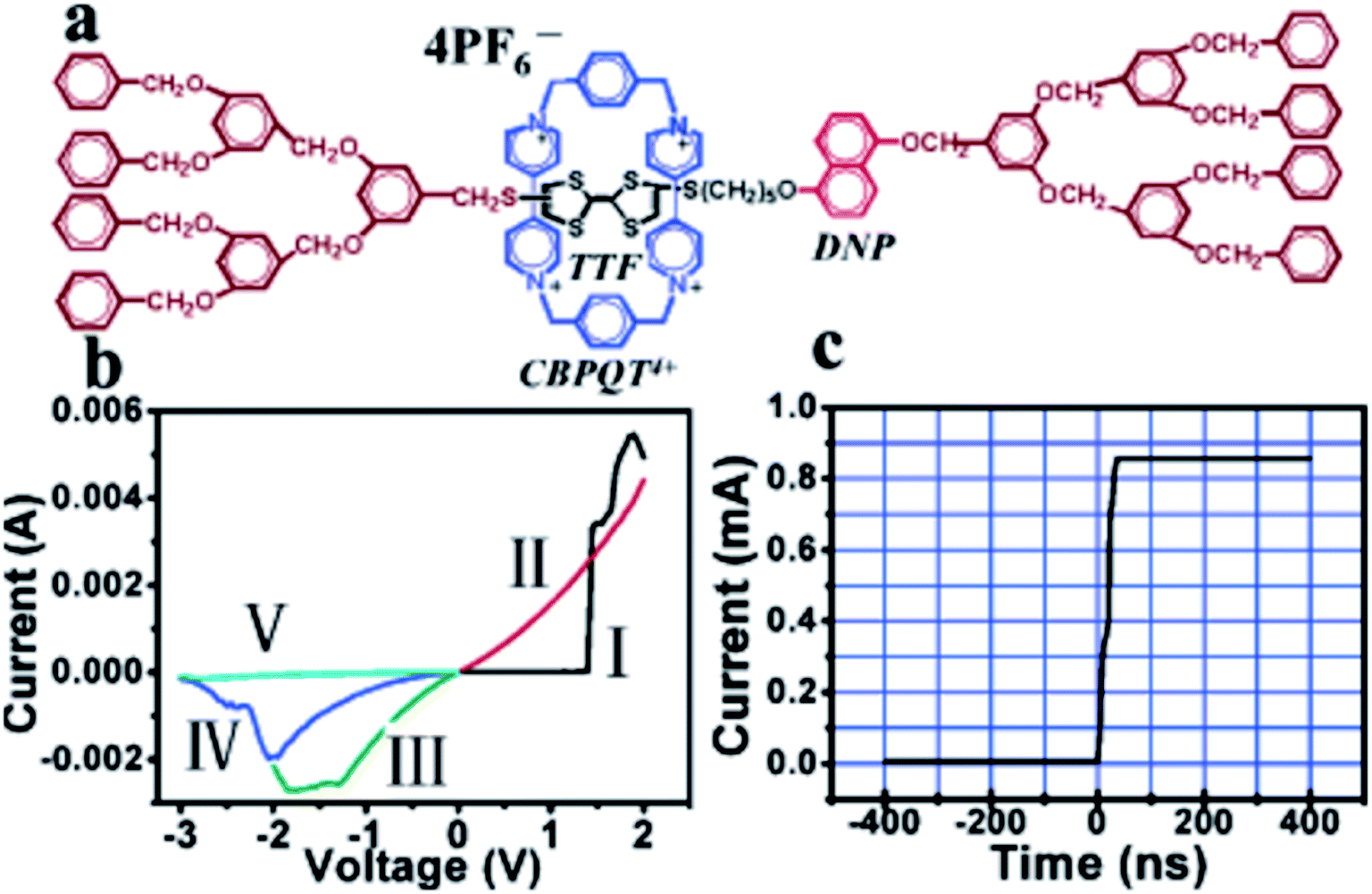 | ||
| Fig. 3 (a) Molecular structure of the rotaxane, H1. (b) I–V characteristics of the thin H1 films on ITO glass, exhibiting the conductance transition from a low- to a high-conductivity state in curve I, the memory effect of the high-conductivity state in curve II, and the recovery of the low-conductivity state with reverse voltage scans in curves III to V. (c) Transition time measurement of the conductance switching, showing a very short transition time of about 60 ns (ref. 93) (printed with permission from ref. 93, Copyright © 2005, American Chemical Society). | ||
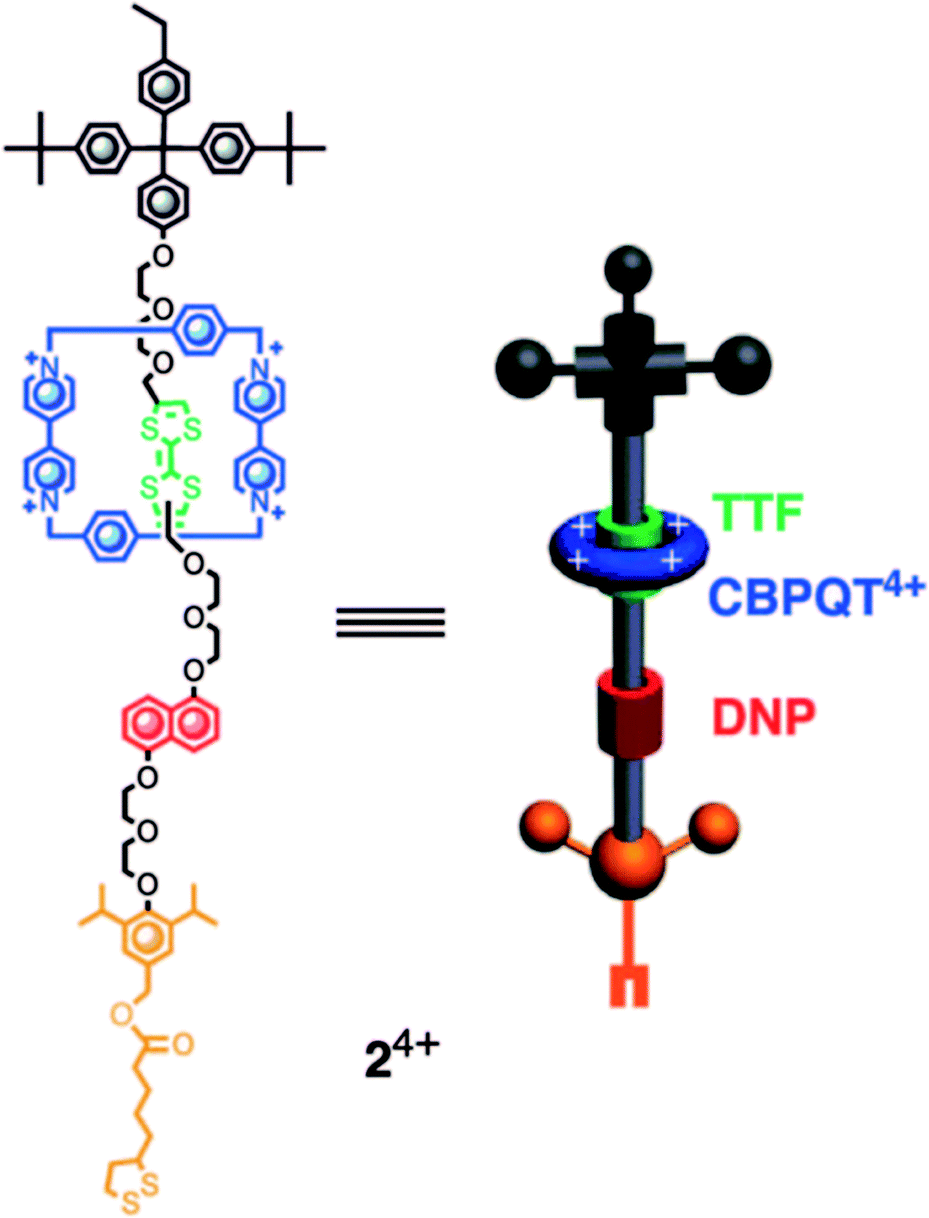
This classic example of a voltage-driven bistable [2]rotaxane structure has one CBPQT4+ macrocycle and one chain with two electron-rich recognition sites (tetrathiafulvalene (TTF) and 1,5-dioxynaphthalene (DNP)).69,83,85,97 Usually, the CBPQT4+ ring stays on the TTF site for a naturally stable state. At this point, the molecule shows a high resistance and low conductance. The shuttling is controlled by the oxidation of the TTF. When the TTF site is oxidized (i.e., losing two electrons), the CBPQT4+ ring leaves the TTF and arrives at the DNP site as a metastable state. As a result, the molecule shows a low resistance and a high conductance. When the TTF site is reduced, and similarly, the DNP site is oxidized, the CBPQT4+ ring translates from DNP back to TTF, and the resistance and conductance change correspondingly. The experiment proved the results of two distinct states: the resistance of one state is 10–100 times that of the other state. Therefore, the switching is achieved by the transition between these two states with different conductivity.84
The reported [2]rotaxane can be used for digital data storage. The reading and writing operations are achieved via a Scanning Tunneling Microscope (STM), as shown in Fig. 12.93 The device implements reproducible nano-recording function. The measured conductance transition showed a very short switching time of about 60 ns. The on/off ratio was about 100 (ref. 93). Moreover, the reversible conductivity switching and non-volatile storage effect of the sample are very stable even if the sample was exposed to air for about 2 months. The series of experiments have also confirmed that the conductivity switch is caused by the macrocycle shuttling in the [2]rotaxane, instead of the formation of metal nanowires.
Green, et al.101 designed a 160 kb [2]rotaxane molecular electronic memory based on a crossbar structure. The [2]rotaxane molecule applied in the crossbar memory is shown in Fig. 4. The memory device contains the following features. First, the wiring is at the micron-level and results in a high bit density (1011 bit per cm2). The size of 16 kb memory is approximately equal to the size of a white blood cell. Secondly, the geometric structure of the crossbar can be manufactured by a traditional top-down nanofabrication process. The crossbar switch is a high-density two-dimensional digital circuit that supports independent addressing for each unit. At the same time, this geometrical structure can tolerate manufacturing defects; that is, the resulting hardware defects do not prevent the configuration of a robust computing device. Although all good bits can be operated in multiple loop times, such as testing and reading/writing steps, most of those bits just fail after about six cycles; also, they do not last for more than ten cycles. Thus, the failure mechanism and long-term reliability of the memory still need to be investigated.
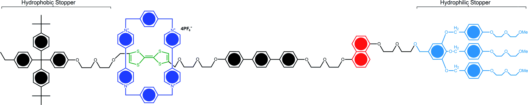 | ||
| Fig. 4 Structural formula of the bistable [2]rotaxane used in the crossbar memory. The ground-state conformation is shown and corresponds to the low-conductance or ‘0’ co-conformation. The molecule is oriented with the (light blue) hydrophilic stopper in contact with the Si bottom-nanowire electrodes. The switching mechanism involves oxidation of the (green) tetrathiafulvalene (TTF) site to the TTF1+ or TTF2+ oxidation state, followed by translation of the blue ring from the TTF1 site to the (red) dioxynaphthalene site. The TTF+ is reduced back to the TTF0 oxidation state to form the metastable state co-conformer, which is the high-conductance or ‘1’ state. The metastable state will relax back to the ground state with a half-life of about an hour101 (printed with permission from ref. 101, Copyright © 2007, Nature Publishing Group). | ||
Furthermore, in this case, [2]rotaxane has the same CBPQT4+ macrocycle and one chain with a TTF site and DNP site as the one in Gao and Feng's work, but the stoppers and spacer are different. Simulations and experiments prove the effect of species of spacers on the switching of the CBPQT4+ macrocycle,84,95,97 where more rigid aromatic spacers will stabilize the switching barrier when designing a molecular device. When the [2]rotaxane molecular switch is used as a memory cell, the reading/writing operation is done by applying a voltage pulse to the electrodes. A “+1.5 V, 0.2 s” pulse is for setting the bit to the “1” state, while a “−1.5 V, 0.2 s” pulse is for setting the bit to the “0” state. A non-perturbing +0.2 V bias is for reading each bit.101 The paper did not verify the switching time of the [2]rotaxane unit. The reported memory is implemented with a nanowire-based crossbar architecture.
Chen, et al.81 fabricated a nano-scale rewritable non-volatile crossbar memory circuit based on a [2]rotaxane monomolecular switch via the imprinting lithography technology. Similarly, this [2]rotaxane, in Fig. 5, has a CBPQT4+ macrocycle and one chain with a DNP site. It does not have a TTF site; instead, it has a mpTTF site. The [2]rotaxane monolayer was fabricated by using the Langmuir–Blodgett (LB) method. In the circuit prototype, the LB film of [2]rotaxane is sandwiched between metal nanowires, forming a Ti/Pt-[2]rotaxane-Ti/Pt crossbar. The width of each nanowire was measured to be ∼40 nm; thus, the active area at each cross point in the circuit was ∼1600 nm2. They fabricated an 8 × 8 crossbar in an area of 1 μm2. Each cross point is used as an active storage junction, so the crossbar switch circuit promises a bit density of 6.4 GB cm−2. The prepared nano-scale molecular circuit can be used as an ultra-high-density memory. The paper also demonstrated a demultiplexer/multiplexer logic integrated with the memory. This is classic work aiming at the level 2 challenge (circuit fabrication) and level 3 challenge (building the logic).
 | ||
| Fig. 5 (a) Schematic representation of the crossbar circuit structure. A monolayer of [2]rotaxane (green) is sandwiched between an array of Pt/Ti nanowires (gold, left–right) on the bottom and an array of Pt/Ti nanowires (gold, up–down) on the top. Before the fabrication of the top nanowires, the entire molecular monolayer is covered with a Ti protective layer, which is etched away isotropically by using the top nanowires as an etch mask, leaving the Ti layer (blue) and molecules under the top Pt nanowires intact. (b) Molecular structure of the bistable [2]rotaxane used to form LB monolayers. The molecule has a hydrophobic (dark green) and a hydrophilic (light blue) stopper. The [2]rotaxane has cyclobis(paraquat-p-phenylene) (dark blue) as the ring component and the supporting counterions are hexafluorophosphate81 (printed with permission from ref. 81, Copyright © 2003, IOP Publishing). | ||
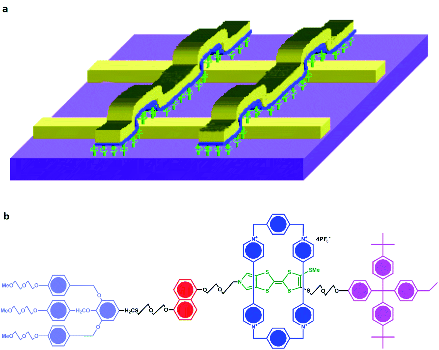
Jia, et al.125 used high-quality graphene as a probe in combination with photoexcitation to establish a redox-bistable [2]rotaxane–graphene interface (in Fig. 6a). The [2]rotaxane (in Fig. 6c) includes a CBPQT4+ macrocycle and one DNP site. The other site is a 4,4′-bipyridinium (BIPY2+) unit. It also has a photocatalytic ruthenium(II)-tris(2,2′-bipyridine) ([Ru(bpy)3]2+) stopper. For operating the switch, photons can be absorbed by [Ru(bpy)3]2+ when light is on. This induces the reduction of the BIPY2+ units, which motivates translocation of the CBPQT4+ macrocycle from the DNP to the BIPY2+ site. When light is out, the CBPQT4+ macrocycle moves back from the BIPY2+ to the DNP site. This work also aims at the design challenges from level 1 to level 3. However, the [2]rotaxane molecule in this work is not directly used as an electronic switch. Instead, the switching is photoactivated and it is composed of both the [2]rotaxane molecule layer and graphene monolayer together (in Fig. 6b). A [2]rotaxane molecule is linked to the graphene layer by a 1-pyrenebutanoic acid (PBA) linker to form a photo-responsive [2]rotaxane–graphene interface.
 | ||
| Fig. 6 (a) Schematic representation of graphene transistors decorated with light-activated switchable [2]rotaxanes in the presence of triethanolamine (TEOA) as a sacrificial electron donor. (b) The two-step strategy employed in the assembly of the bistable [2]rotaxane molecules onto a graphene surface without altering the structure and properties of graphene covalently. (c) The structural formulas and graphical representations of the 1-pyrenebutanoic acid (PBA) used to link the bistable [2]rotaxane molecules noncovalently to the surface of the graphene125 (printed with permission from ref. 125, Copyright © 2013, WILEY-VCH Verlag GmbH & Co. KGaA, Weinheim). | ||
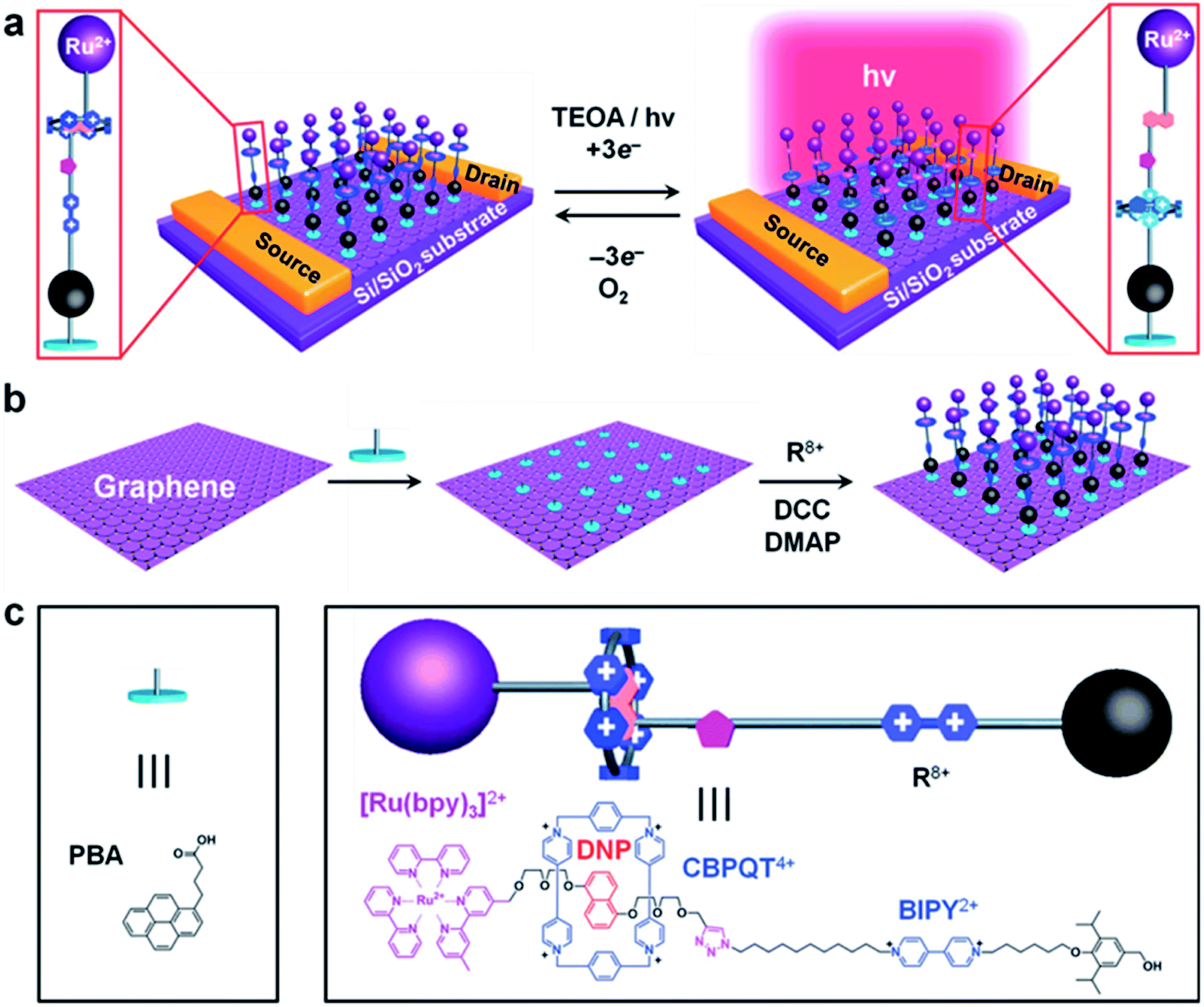
The [2]rotaxane molecular layer forms a positively charged three-group complex after photoactivation if light is given. It makes the CBPQT4+ macrocycle of the [2]rotaxane molecular layer transfer to the BIPY2+ site (at the same time, the CBPQT4+ macrocycle is close to the surface of the graphene layer). As a result, a built-in electric field is formed at the [2]rotaxane–graphene interface. This electric field changes with the shuttle movement of the [2]rotaxane molecular layer and the change of the electrostatically induced capacitance coupling, thereby changing the conductivity of the graphene layer; and finally, the logic states of “ON” and “OFF” (in Fig. 7) are achieved.
 | ||
| Fig. 7 Synergistic photoswitching mechanisms operative in the bistable [2]rotaxane decorated graphene and energy-level diagram of the bistable [2]rotaxane/graphene interface125 (printed with permission from ref. 125, Copyright © 2013, WILEY-VCH Verlag GmbH & Co. KGaA, Weinheim). | ||
For the level 3 challenge, an example research study demonstrated the design and implementation of a half adder and a half subtractor with complex I/O settings. The designed interface implements a multifunctional optoelectronic device, a symmetrical mirror-image optical molecular switch. Its frame system includes microfluidic channels about 100 μm high and about 250 μm wide. The switching time of the switch is about 400 seconds. Each unit shows a non-volatile storage effect and excellent reversibility. The experiment also explored the assignment of binary logic states to the light response behavior of the device, which proved the feasibility of sequential logic circuits design with the memory effect.
Regarding the photo-responsive [2]rotaxane interface, earlier papers were about the study of [2]rotaxane–graphene oxide (GO) surface arrays. Hong Yan, et al.121 introduced photo-response α-CD-based [2]rotaxane onto the surface of GO by applying click chemistry. The macrocycle of [2]rotaxane is a photoswitchable α-cyclodextrin (α-CD). The two recognition sites are the azobenzene unit and the triazole ring on the chain. In the study, GO was functionalized (with carboxylic acid groups) to further enhance its solubility in water. In an aqueous solution, the α-CD ring can be reversibly switched between the two recognition sites in the system via irradiating ultraviolet and visible light alternately. Such [2]rotaxane (in Fig. 8) on functionalized GO provides a photo-response platform for potential information storage devices.
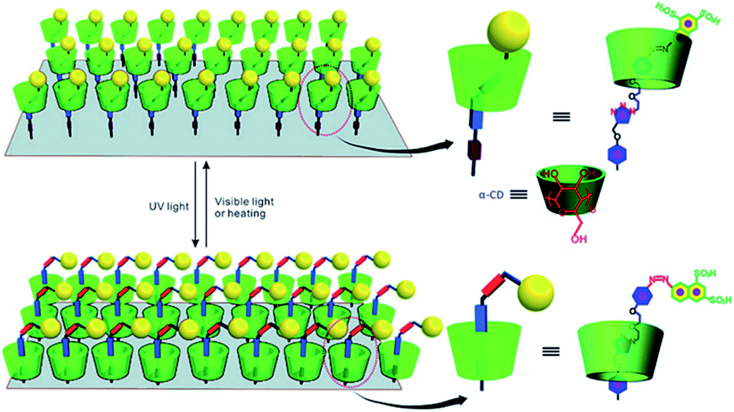 | ||
| Fig. 8 The scheme of a graphic representation of trans–cis photoisomerization of GO functionalized with a [2]rotaxane array. The [2]rotaxane array was attached covalently onto both sides of GO; only functionalization on one side of GO is presented for the sake of clarity121 (printed with permission from ref. 121, Copyright © 2012, WILEY-VCH Verlag GmbH & Co. KGaA, Weinheim). | ||
Brouwer, et al.71 also reported a light-responsive [2]rotaxane. At room temperature, giving a nanosecond laser pulse as the input, the macrocycle moves reversibly between two hydrogen-bonding stations. The macrocycle initially stays at the preferred succinamide (succ) site; and the other site is a 3,6-di-tert-butyl-1,8-naphthalimide (ni) unit. When a light-responsive reaction occurs, the relative binding potentials of the two sites are changed. The benzylic amide macrocycle leaves the succ site and moves to the now-preferred ni site. The switching process of the macrocycle takes about 1 μs. After the charge recombination is completed in 100 μs, the macrocycle returns to the original position. The entire process is reversibly cyclable like the working principle of a piston or a boomerang.
The paper firstly characterized [2]rotaxane and studied the shuttle mechanism, as demonstrated in Fig. 9. In addition, the paper studied the influence of the medium on the shuttling speed of the macrocycle. The speed of the shuttle process involves the breaking of the H-bond between the macrocycle and the site. The macrocycle will shuttle faster in a solvent with a higher dielectric constant and shuttle slower in a solvent with a lower dielectric constant. For polarity, a solvent with a higher polarity will lead to a higher shuttle speed. This result is also in good agreement with the lubricating effect of water during [2]rotaxane molecular switching. Although the paper did not mention the speed at which the macrocycle returns to the initial site, the confirmed forward switching time was about 1 μs. However, the charge recombination rate of the rotaxane radical anion is relatively slow and requires about 100 μs (about 100 times that of the forward switching process). Thus, the cycle rate of the switching process will depend on the “charge recovery rate”. In addition, the energy of forward switching movement is about 4.3 kcal mol−1, while the backward process (recovery stroke) released an energy of about 6.9 kcal mol−1. The hypothesis is that forward and backward processes are non-symmetrical. The paper also suggested that longer wavelength light applied may result in a shorter switching time if binding properties between the macrocycle and the station as well as the physical properties of the chromophore are adjusted.
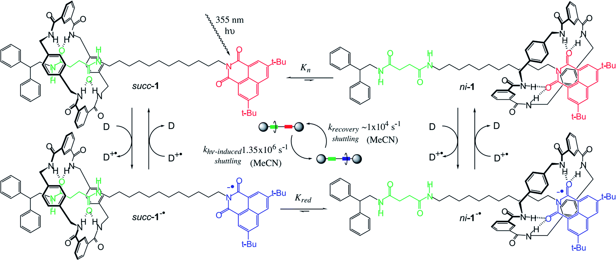 | ||
| Fig. 9 The scheme of a photoresponsive, H-bond-assembled, molecular shuttle 1. Before the 355 nm laser pulse, the translational coconformer succ-1 is predominant because the ni station is a poor H-bond acceptor (Kn < 0.01). After photoreduction by an external donor (D; DABCO, TMPD, or biphenyl), the equilibrium between succ-1−˙ and ni-1−˙ changes (Kred > 1500) because ni−˙ is a powerful H-bond acceptor and back-electron transfer is slow (spin forbidden). Because the absorption maximum (λmax) of ni-1−˙ is located at shorter wavelengths than that of succ-1−˙, the sum of the absorptions shifts to the blue. The rate at which the absorption shifts (kshift) is related to the rate of change in the relative populations of succ-1−˙ and ni-1−˙, i.e., the time taken for light-induced shuttling of the macrocycle (∼1 μs, MeCN). After charge recombination (∼100 μs, MeCN), the macrocycle shuttles back to its original position. Cycling of this process at 104 times per second generates a mechanical power of ∼10−15 W for each shuttle71 (printed with permission from ref. 71, Copyright © 2001, The American Association for the Advancement of Science). | ||
Zheng et al.107 fabricated a [2]rotaxane-Au nanodisk array. The bistable [2]rotaxane (Fig. 10) is redox-controllable by the oxidants and reductants it is exposed to. The localized surface plasmon resonances (LSPRs) of the gold nanodisk will undergo reversible conversion. This property shows the promise of application of the device in nanophotonic integrated circuits.
 | ||
| Fig. 10 Molecular formulas and graphical representations of the bistable [2]rotaxane107 (printed with permission from ref. 107, Copyright © 2009, American Chemical Society). | ||
In order to implement functional nano-electronic circuits and make it easily compatible with current microelectronic circuits, some practical challenges need to be addressed. Table 1 compares some core features of [2]rotaxane molecular switches with different driving methods: voltage-driven, photon-driven, and chemical-driven. Among these three driving methods, the voltage-driven has more advantages compared to the other two. First, the input and output signals of voltage-driven [2]rotaxane are all electrical signals, which are compatible with current microelectric circuits. The voltage-driven [2]rotaxane also shows less response time and switching time compared to the other two driving methods.
| Driving methods | Inputs | Outputs | Response time | Switching time | Waste products | Solvent required | Fabrication |
|---|---|---|---|---|---|---|---|
| Voltage-driven | Voltage | Voltage | Fast | Fastest case: ∼ns | No | No | Metal–molecule–metal |
| Current | The structure is simple | ||||||
| Light | Other cases: ∼ps | Low cost | |||||
| Fluorescence | Decreased complexity at the system level | ||||||
| Photo-driven | Light | Light | Relatively fast | Fastest case: ∼μs | No | Yes | Need additional parts as the light path for control |
| Fluorescence | The structure is complex | ||||||
| Chirality | Other cases: ∼ms | Reliability is decreased | |||||
| Current | Increased complexity at the system level | ||||||
| Chemical-driven | Chemical | Light | Relatively slow | Fastest case: ∼μs | Yes | Yes | Rely on a liquid environment |
| Current | Need chemical supplement and by-product removal | ||||||
| Chirality | 2nd fastest case: ∼ms | The structure is complex | |||||
| Chemicals | Reliability is decreased | ||||||
| Other cases:∼s | Increased complexity at the system level |
Second, voltage-driven [2]rotaxane uses a solid-state device under an appropriate working environment and no liquid solution is needed. All three types of driving methods of [2]rotaxane switches can work at room temperature. However, the photo-driven [2]rotaxane needs an additional physical structure to transport solvents and control the light path, and the array usually needs to work at the interface with the solvent as the medium. Therefore, they have longer operated delays in time. In a chemical-drive system, chemical reagents are required as signal inputs and its performance will be more sensitive to temperature. Both cases require molecules to perform in a stable solvent environment, which adds extra complexity to the system. For chemical-driven [2]rotaxane, chemical reagents need to be added and by-products need to be removed. In contrast, the voltage-driven [2]rotaxane switch does not require a liquid solution environment and chemical reagents.
To build a nano-scale circuit, a large number of molecules need to stably link to the electrodes, and the circuit will be controllably integrated with external components to execute either memory or logic functions. Furthermore, an efficient architecture should be incorporated to allow the device to communicate with other systems and operate in a collaborative way. The comparison of the three driving methods of [2]rotaxane switches is listed in Table 1. Besides, a complete list of essential research works on rotaxanes over years at all three levels of the pyramid are summarized in Table 2.
For [2]rotaxane molecular circuits, the fundamental research and level 1 research are relatively mature. A variety of [2]rotaxanes have been synthesized in practice, and their characteristics as molecular switches have been characterized. As the level 1 challenge, the design of molecular electronic components needs to consider the driving method of the [2]rotaxane molecular switch, its working environment, the response signals, and the switching time (performance).
| Year | Title | Type | Items | Method | Authors | |
|---|---|---|---|---|---|---|
| a The table mainly collected articles of [2]rotaxane. | ||||||
| 1981 | Relatively high-yield syntheses of rotaxanes. Syntheses and properties of compounds consisting of cyclodextrins threaded by .alpha.,.omega.-diaminoalkanes coordinated to cobalt(III) complexes | Fundamental | Synthesis; characterization | Experiment | N/A | Ogino, et al.52 |
| 1984 | Synthesis and properties of rotaxane complexes. (2) Rotaxanes consisting of alpha- or beta-cyclodextrins threaded by (.mu.-.alpha.,.omega.-diaminoalkane)bis[chlorobis(ethylenediamine)cobalt(III)] complexes | Fundamental | Synthesis; characterization | Experiment | N/A | Ogino, et al.53 |
| 1991 | Synthesis of a rotaxane via the template method | Fundamental | Synthesis | Experiment | N/A | Wu, et al.54 |
| 1992 | Cyclobis(paraquat-p-phenylene) as a synthetic receptor for electron-rich aromatic compounds: electrochemical and spectroscopic studies of neurotransmitter binding | Fundamental | Synthetic electron receptor; characterization; CV | Experiment, calculation | N/A | Bernardo, et al.55 |
| 1993 | A light-induced molecular shuttle based on a [2]rotaxane-derived triad | Level 1 | Synthesis; characterization; CV | Experiment | ∼10 ns | Benniston, et al.56 |
| Fundamental | ||||||
| 1994 | A chemically and electrochemically switchable molecular shuttle | Level 1 | Characterization | Experiment | N/A | Bissell, et al.57 |
| Fundamental | ||||||
| 1997 | The self-assembly of a switchable [2]rotaxane | Fundamental | Synthesis; characterization | Experiment | N/A | Martínez-Díaz, et al.58 |
| 1997 | A light-driven molecular shuttle based on a rotaxane | Level 1 | Light-driven molecular shuttle; characterization | Experiment | N/A | Murakami, et al.59 |
| Fundamental | ||||||
| 1998 | Molecular shuttles. A computational study (MM and MD) on the translational isomerism in some [2]rotaxanes | Fundamental | Molecular dynamics | Simulation | N/A | Grabuleda, et al.60 |
| 1999 | Rotaxane formation under thermodynamic control | Fundamental | Synthesis | Experiment | N/A | Cantrill, et al.61 |
| 1999 | High-yielding rotaxane synthesis with an anion template | Fundamental | Synthesis | Experiment | N/A | Hübner, et al.62 |
| 1999 | A new protocol for rotaxane synthesis | Fundamental | Synthesis | Experiment | N/A | Cantrill, et al.63 |
| 1999 | Electronically configurable molecular-based logic gates | Level 3 | Rotaxanes sandwiched between metal electrodes; CV; logic gate configuration | Experiment | N/A | Collier, et al.64 |
| Fundamental | ||||||
| 2000 | Rotaxane-based molecular switch with fluorescence signaling | Level 1 | Synthesis; acid–base driven; fluorescence response | Experiment | N/A | Jun, et al.65 |
| Fundamental | ||||||
| 2000 | A [2]catenane-based solid state electronically reconfigurable switch | Level 2 | [2]Catenane-based; solid state memory device; voltage controllable; fabrication; CV; switching mechanism | Experiment | N/A | Collier, et al.66 |
| 2000 | Current/voltage characteristics of monolayers of redox-switchable [2]catenanes on gold | Level 2 | CV characterization | Experiment | N/A | Asakawa, et al.67 |
| 2001 | Enhanced hydrogen bonding induced by optical excitation: unexpected subnanosecond photoinduced dynamics in a peptide-based [2]rotaxane | Fundamental | Characterization; synthesis; shuttling process | Experiment | ∼ns | Wurpel, et al.68 |
| 2001 | Slow shuttling in an amphiphilic bistable [2]rotaxane incorporating a tetrathiafulvalene unit | Fundamental | Characterization; color change in the switching process | Experiment | N/A | Jeppesen, et al.69 |
| 2001 | Switching devices based on interlocked molecules | Level 2 | Two-terminal MSTJ; interfaces; characterization; CV; electronically Configurable logic gates | Experiment | N/A | Pease, et al.70 |
| Fundamental | ||||||
| 2001 | Photoinduction of fast, reversible translational motion in a hydrogen-bonded molecular shuttle | Fundamental | Photoinduced shuttling; characterization | Experiment | ∼1 μs | Brouwer, et al.71 |
| 2001 | Molecular-based electronically switchable tunnel junction devices | Level 2 | Synthesis; characterization; solution-state characterization; solid-state device fabrication; LB film; MSTJ; CV; cycling and volatility; voltage controlled diode behavior | Experiment | N/A | Collier, et al.72 |
| 2002 | Switching “ON” and “OFF” the expression of chirality in peptide rotaxanes | Fundamental | Chirality | Experiment | N/A | Asakawa, et al.73 |
| Simulation | ||||||
| 2002 | An acid–base switchable [2]rotaxane | Fundamental | Synthesis; characterization | Experiment | N/A | Elizarov, et al.74 |
| 2003 | Electrochemically switchable hydrogen-bonded molecular shuttles | Fundamental | Synthesis; characterization; CV; chemical oxidation/reduction and shuttle control | Simulation | ∼50 μs | Altieri, et al.75 |
| Experiment | ||||||
| 2003 | Shuttling process in [2]rotaxanes. Modeling by molecular dynamics and free energy perturbation simulations | Level 1 | Molecular dynamics; free energy calculations | Simulation | N/A | Grabuleda, et al.76 |
| Fundamental | ||||||
| 2003 | Assembly of an electronically switchable rotaxane on the surface of a titanium dioxide nanoparticle | Level 2 | [2]Rotaxane-TiO2 film; adsorption; characterization; synthesis; CV | Experiment | N/A | Long, et al.77 |
| Fundamental | ||||||
| 2003 | The molecule–electrode interface in single molecule transistors | Level 2 | Pt/[2]rotaxane/Pt transistor; characterization; molecule–electrode contact | Experiment | N/A | Yu, et al.78 |
| 2003 | Molecule-independent electrical switching in Pt/organic monolayer/Ti devices | Level 2 | Pt/[2]rotaxane/Ti; LB film; crossbar; voltage controllable; CV; resistance | Experiment | N/A | Stewart, et al.79 |
| 2003 | Nanoscale molecular-switch devices fabricated by imprint lithography | Level 2 | Nano-imprinting; circuit fabrication | Experiment | N/A | Chen, et al.80 |
| 2003 | Nanoscale molecular-switch cross bar circuits | Level 3 | Pt/Ti/[2]rotaxane/Pt crossbar; nano-imprinting; circuit fabrication; memory operation; logic configuration | Experiment | N/A | Chen, et al.81 |
| 2004 | Density functional theory studies of the [2]rotaxane component of the Stoddart-Heath molecular switch | Fundamental | Potential energy calculations; net electrostatic potential | Calculation | N/A | Jang, et al.82 |
| 2004 | Redox-controllable amphiphilic [2]rotaxanes | Level 1 | Synthesis; characterization; chemical oxidation/reduction and shuttle control | Experiment | N/A | Tseng, et al.83 |
| Fundamental | ||||||
| 2004 | Mechanism of the Stoddart-Heath bistable rotaxane molecular switch | Level 1 | CV; conductance calculations | Simulation | N/A | Deng, et al.84 |
| Fundamental | ||||||
| 2004 | Molecular shuttles based on tetrathiafulvalene units and 1,5-dioxynaphthalene ring systems | Level 2 | Synthesis; characterization; MSTJ; energy barrier; kinetic; thermodynamic | Experiment | N/A | Kang, et al.85 |
| Fundamental | ||||||
| 2004 | Electromechanics of a redox-active rotaxane in a monolayer assembly on an electrode | Level 2 | Characterization; CV; impedance spectra; the medium; electrochemical/contact angle measurements | Experiment | N/A | Katz, et al.86 |
| Fundamental | ||||||
| 2005 | Molecular dynamics simulation of amphiphilic bistable [2]rotaxane Langmuir monolayers at the air/water interface | Fundamental | Molecular dynamics; LB film air/water interface; mpTTF | Simulation | N/A | Jang, et al.87 |
| Calculation | ||||||
| 2005 | Shuttling dynamics in an acid–base-switchable [2]rotaxane | Fundamental | Acid–base controlled shuttling kinetics; thermodynamics | Experiment | ∼s | Garaudée, et al.88 |
| ∼ms | ||||||
| 2005 | Temperature-dependent and friction-controlled electrochemically induced shuttling along molecular strings associated with electrodes | Fundamental | The temperature and solvent dependence shuttling; friction phenomena; characterization; CV | Experiment | N/A | Katz, et al.89 |
| 2005 | Experimental and theoretical study of the adsorption of fumaramide [2]rotaxane on Au(111) and Ag(111) surfaces | Level 2 | Characterization; molecular dynamics; adsorption; fumaramide [2]rotaxane film on Au(111) and Ag(111) | Experiment | N/A | Mendoza, et al.90 |
| Fundamental | Simulation | |||||
| 2005 | Structures and properties of self-assembled monolayers of bistable [2]rotaxanes on Au(111) surfaces from molecular dynamics simulations validated with experiment | Level 2 | Molecular dynamics; rotaxane SAMs; [2]rotaxane-Au(111); interface | Simulation | N/A | Jang, et al.91 |
| Fundamental | ||||||
| 2005 | Molecular mechanics and molecular electronics | Level 3 | Crossbar architecture; characterization; CV; MSTJ; SNAP; crosspoint memory and logic circuit | Experiment | N/A | Beckman, et al.92 |
| 2005 | Stable, reproducible nanorecording on rotaxane thin films | Level 3 | Characterization; STM for nano-recording; LB film on a HOPG substrate; CV | Experiment | ∼60 ns | Feng, et al.93 |
| 2006 | Ground-state equilibrium thermodynamics and switching kinetics of bistable [2]rotaxanes switched in solution, polymer gels, and molecular electronic devices | Level 1 | Thermodynamics; switching kinetics; synthesis; characterization; CV | Experiment | N/A | Choi, et al.94 |
| Fundamental | ||||||
| 2006 | Mechanism of oxidative shuttling for [2]rotaxane in a Stoddart-Heath molecular switch: density functional theory study with a continuum-solvation model | Level 1 | The quantum mechanics study of the mechanism; molecular dynamics | Simulation | N/A | Jang, et al.95 |
| Fundamental | ||||||
| 2006 | Structural and conductance transitions of rotaxane based nanostructures and application in nanorecording | Level 3 | Conductance transitions; STM; LB film on a HOPG substrate; characterization; CV; memory operation; stability | Experiment | ∼60 ns | Gao, et al.96 |
| Simulation | ||||||
| 2007 | Tetrathiafulvalene-, 1,5-dioxynaphthalene-, and cyclobis(paraquat-p-phenylene)-based [2]rotaxanes with cyclohexyl and alkyl chains as spacers: synthesis, Langmuir–Blodgett films, and electrical bistability | Fundamental | Synthesis; characterization; LB films; CV | Experiment | N/A | Guo, et al.97 |
| 2007 | A redox-driven multicomponent molecular shuttle | Fundamental | Synthesis; characterization; CV | Experiment | N/A | Saha, et al.98 |
| 2007 | Linking molecular switches to platinum electrodes studied with DFT | Level 2 | Pt/[2]rotaxane/Pt; metal/organic interface; DFT calculation | Experiment | N/A | Jacob, et al.99 |
| Fundamental | Calculation | |||||
| 2007 | Efficiency of π–π tunneling in [2]rotaxane molecular electronic switches | Level 2 | Au/[2]rotaxane/Au; molecule-electrode configurations; charge transport and energetic characterization | Simulation | N/A | Kim, et al.100 |
| Fundamental | Calculation | |||||
| 2007 | A 160 kilobit molecular electronic memory patterned at 1011 bits per square centimetre | Level 3 | Crossbar memory; defect-tolerant circuit architecture; nano-imprinting | Experiment | N/A | Green, et al.101 |
| 2007 | Reversible, erasable, and rewritable nanorecording on an H2 rotaxane thin film | Level 3 | Characterization; STM for nano-recording; LB film; ITO and HOPG substrates; CV | Experiment | N/A | Feng, et al.102 |
| 2008 | A redox-switchable r-cyclodextrin-based [2]rotaxane | Fundamental | Synthesis; characterization; CV | Experiment | N/A | Zhao, et al.103 |
| 2009 | A rapidly shuttling copper-complexed [2]rotaxane with three different chelating groups in its axis | Fundamental | Characterization; CV | Experiment | N/A | Collin, et al.104 |
| 2009 | Squaraine rotaxanes with boat conformation macrocycles | Fundamental | Boat conformation macrocycles; characterization | Experiment | N/A | Fu, et al.105 |
| 2009 | First-principles studies of the dynamics of [2]rotaxane molecular switches | Level 1 | DFT calculation; energetics of the switching; ionization potentials; switching speed of the crossbar array; electrostatic screening properties | Simulation | ∼μs | Phoa, et al.106 |
| Fundamental | Calculation | |||||
| 2009 | Active molecular plasmonics: controlling plasmon resonances with molecular switches | Level 3 | [2]Rotaxane-Au nanodisk array; characterization | Experiment | N/A | Zheng, et al.107 |
| Simulation | ||||||
| 2010 | Excited state distortions in a charge transfer state of a donor–acceptor [2]rotaxane | Fundamental | Characterization; DFT calculation | Experiment | N/A | Stephenson, et al.108 |
| Calculation | ||||||
| 2010 | Self-assembly, stability quantification, controlled molecular switching, and sensing properties of an anthracene-containing dynamic [2]rotaxane | Fundamental | Synthesis; characterization; effect of salt; molecular switching at different acid concentrations | Experiment | N/A | Wong, et al.109 |
| 2010 | Changing stations in single bistable rotaxane molecules under electrochemical control | Level 2 | Synthesis; characterization; voltage controllable; solid-state switch fabrication; tunneling current | Experiment | N/A | Ye, et al.110 |
| 2011 | A neutral redox-switchable [2]rotaxane | Fundamental | Synthesis; characterization; CV | Experiment | N/A | Olsen, et al.111 |
| 2011 | Conformational analysis and UV/Vis spectroscopic properties of a rotaxane-based molecular machine in acetonitrile dilute solution: when simulations meet experiments | Fundamental | Molecular dynamics; free energy calculations; characterization | Simulation | N/A | Mancini, et al.112 |
| Calculation | ||||||
| 2011 | Electrostatic barriers in rotaxanes and pseudorotaxanes | Fundamental | Synthesis; characterization; the thermodynamics and the kinetics | Experiment | N/A | Hmadeh, et al.113 |
| 2011 | The switching of rotaxane-based motors | Fundamental | Molecular dynamics; structural and energetic properties | Simulation | ∼10 ns | Lee, et al.114 |
| 2011 | A redox-active reverse donor–acceptor bistable [2]rotaxane | Fundamental | Synthesis; characterization; molecular dynamics; CV; DPV | Experiment | N/A | Dey, et al.115 |
| 2011 | Origin of the redox-induced conductance transition in a thin film of switchable rotaxanes | Level 1 | Mobility calculations; conductance calculations; reorganization energy calculations | Calculation | N/A | Rossi, et al.116 |
| Fundamental | ||||||
| 2011 | Computational investigation of the role of counterions and reorganization energy in a switchable bistable [2]rotaxane | Level 1 | Reorganization energy; conductivity | Calculation | N/A | Foster, et al.117 |
| Fundamental | ||||||
| 2011 | A solid-state switch containing an electrochemically switchable bistable poly[n]rotaxane | Level 2 | Synthesis; characterization; solid-state switch fabrication; CV; Au/polymer/Ti/Au | Experiment | N/A | Zhang, et al.118 |
| 2012 | Solvent-controlled shuttling in a molecular switch | Fundamental | Molecular dynamics; free energy calculations; solvent-driven switching; temperature-driven switching | Simulation | N/A | Liu, et al.119 |
| 2012 | Mechanically induced intramolecular electron transfer in a mixed-valence molecular shuttle | Level 1 | Synthesis; characterization; CV; activation energy for electron transfer | Experiment | N/A | Barnes, et al.120 |
| Fundamental | Calculation | |||||
| 2012 | A photoswitchable [2]rotaxane array on graphene oxide | Level 2 | [2]Rotaxane-GO array; [2]rotaxane array | Experiment | N/A | Yan, et al.121 |
| 2012 | Electron transfer and switching in rigid [2]rotaxanes adsorbed on TiO2 nanoparticles | Level 2 | [2]Rotaxane-TiO2 interface; adsorption; characterization; CV; SET; voltage controlled shuttling | Experiment | N/A | Lestini, et al.122 |
| 2013 | A piston-rotaxane with two potential stripes: force transitions and yield stresses | Fundamental | Force transitions; yield stresses | Calculation | N/A | Sevick, et al.123 |
| 2013 | Water lubricates hydrogen-bonded molecular machines | Fundamental | Characterization; lubricating role of water | Experiment | N/A | Panman, et al.124 |
| 2013 | Interface-engineered bistable [2]rotaxane–graphene hybrids with logic capabilities | Level 3 | [2]Rotaxane–graphene interface; light-activated switch; fabrication; characterization; logic configuration | Experiment | ∼400 s | Jia, et al.125 |
| 2015 | A redox-controllable molecular switch based on weak recognition of BPX26C6 at a diphenylurea station | Fundamental | Synthesis; characterization | Experiment | N/A | Chang, et al.126 |
| 2015 | The true nature of rotary movements in rotaxanes | Fundamental | Molecular dynamics; free-energy barriers | Simulation | N/A | Liu, et al.127 |
| 2015 | A fluorescent bistable [2]rotaxane molecular switch on SiO2 nanoparticles | Level 2 | [2]Rotaxane-SiO2; adsorption; characterization; non-solid interface; acid–base controlled fluorescent switching | Experiment | N/A | Cao, et al.128 |
| Fundamental | ||||||
| 2016 | Molecular dynamics simulations of acid/base induced switching of a bistable rotaxane | Fundamental | Molecular dynamics; effects of different solvents | Simulation | ∼ps | Halstead, et al.129 |
| 2016 | Superior anion induced shuttling behaviour exhibited by a halogen bonding two station rotaxane | Fundamental | Characterization; synthesis; halogen bonding and donor–acceptor charge-transfer interactions | Experiment | N/A | Barendt, et al.130 |
| 2016 | Effect of component mobility on the properties of macromolecular [2]rotaxanes | Fundamental | Synthesis; topological transformation | Experiment | N/A | Chen, et al.131 |
| 2016 | How does the solvent modulate shuttling in a pillararene/imidazolium [2]rotaxane? Insights from free energy calculations | Level 1 | Molecular dynamics; free energy calculations; solvent interactions | Simulation | N/A | Liu, et al.132 |
| Fundamental | ||||||
| 2016 | Performance of some DFT functionals with dispersion on modeling of the translational isomers of a solvent-switchable [2]rotaxane | Fundamental | DFT studies; molecular mechanics | Simulation | N/A | Ivanov, et al.133 |
| 2017 | The lubricating role of water in the shuttling of rotaxanes | Fundamental | Hydrogen-bonding interactions; effects of different solvents; lubricating role of water | Simulation | N/A | Fu, et al.134 |
| 2017 | Remote photoregulated ring gliding in a [2]rotaxane via a molecular effector | Fundamental | Characterization; light-driven chemical communication | Experiment | N/A | Tron, et al.135 |
| 2017 | A divalent pentastable redox-switchable donor–acceptor rotaxane | Fundamental | Synthesis; characterization; DFT calculations | Experiment | N/A | Schröder, et al.136 |
| Calculation | ||||||
| 2017 | Highly elastic binders integrating polyrotaxanes for silicon microparticle anodes in lithium ion batteries | Polytrioxanes | Synthesis; characterization; electrode–electrolyte interface | Experiment | N/A | Choi, et al.137 |
| Level 2 | ||||||
| 2018 | Chirality in rotaxanes and catenanes | Fundamental | Chirality in rotaxanes and catenanes | Theoretical | N/A | Jamieson, et al.138 |
| 2018 | Fault detection and analysis of a bistable rotaxane molecular electronic switch – a simulation approach | Level 2 | Molecular defects in crossbar architecture | Simulation | N/A | Kumar, et al.139 |
| 2018 | A gold-nanoparticle stoppered [2]rotaxane | Level 2 | Gold-nanoparticle–[2]rotaxane interface | Experiment | N/A | Ulfkjær, et al.140 |
| 2018 | Bistable [2]rotaxane encoding an orthogonally tunable fluorescent molecular system including white-light emission | Fundamental | Fluorescent molecular switches; characterization | Experiment | N/A | Liu, et al.141 |
| 2018 | Higher-generation type III-B rotaxane dendrimers with controlling particle size in three-dimensional molecular switching | Dendrimer | Synthesis; characterization; controllable particle size | Experiment | N/A | Kwan, et al.142 |
| 2018 | Dual stimuli-responsive rotaxane-branched dendrimers with reversible dimension modulation | Dendrimer | Synthesis; characterization; reversible dimension modulation | Experiment | N/A | Wang, et al.143 |
| 2019 | pH-controlled fluorescence probes for rotaxane isomerization | Fundamental | Free-energy; mechanism of the pH-controlled optical switch | Experiment | N/A | Zhang, et al.144 |
| 2019 | Accelerating the shuttling in hydrogen-bonded rotaxanes: active role of the axle and the end station | Fundamental | Photoswitchable molecular shuttle; characterization; the shuttling rate and mechanism; shuttling dynamics | Experiment | ∼30 ns | Kumpulainen, et al.145 |
| 2019 | Influence of the ring position on the temporal dependence of charge movement in a switchable [2]rotaxane | Level 1 | Mechanism of electron transit | Simulation | ∼ns | Bazargan, et al.146 |
| Fundamental | ||||||
| 2019 | A [2]rotaxane-based circularly polarized luminescence switch | Level 1 | Synthesis; characterization; circularly polarized luminescence (CPL); chemical-driven switching | Experiment | N/A | David, et al.147 |
| 2019 | Chemical ON/OFF switching of mechanically planar chirality and chiral anion recognition in a [2]rotaxane molecular shuttle | Level 1 | Characterization; planar chirality; chemical-driven switching | Experiment | N/A | Corra, et al.148 |
| 2019 | Carbon nanostructures in rotaxane architectures | Fundamental | Rotaxanes based on fullerenes and carbon nanotubes | N/A | N/A | Barrejón, et al.149 |
| 2019 | Construction of type III-C rotaxane-branched dendrimers and their anion-induced dimension modulation feature | Dendrimer | Synthesis; characterization; dimension modulation | Experiment | N/A | Wang, et al.150 |
| 2019 | Type III-C rotaxane dendrimers: synthesis, dual size modulation and in vivo evaluation | Fundamental | Synthesis; characterization | Experiment | N/A | Kwan, et al.151 |
| 2019 | A supramolecular network derived by rotaxane tethering three ureido pyrimidinone groups | Fundamental | A supramolecular network; characterization | Experiment | N/A | Rao, et al.152 |
| 2020 | Electrochemical switching of a fluorescent molecular rotor embedded within a bistable rotaxane | Level 1 | Synthesis; characterization; CV; energy calculation; fluorescence; voltage-driven switching | Experiment | N/A | Wu, et al.153 |
| Calculation | ||||||
| 2020 | Switchable polymer materials controlled by rotaxane macromolecular switches | Fundamental | Synthesis; topological transformation | Experiment | N/A | Takata, et al.154 |
| 2020 | Synthesis of a mechanically planar chiral rotaxane ligand for enantioselective catalysis | Fundamental | Synthesis; characterization; a mechanically planar chiral rotaxane for catalytically active gold ions | Experiment | N/A | Heard, et al.155 |
| 2020 | Thermodynamic and electrochemical study of tailor-made crown ethers for redox-switchable (pseudo)rotaxanes | Fundamental | Synthesis; characterization; thermodynamics; electrochemistry | Experiment | N/A | Hupatz, et al.156 |
| 2020 | Daisy chain dendrimers: integrated mechanically interlocked molecules with stimuli-induced dimension modulation features | Dendrimer | Daisy chain dendrimers; synthesis; characterization | Experiment | N/A | Li, et al.157 |
| 2020 | Development and advancement of rotaxane dendrimers as switchable macromolecular machines | Dendrimer | Synthesis; characterization | N/A | N/A | Kwan, et al.158 |
| 2021 | Covalent [2]catenane and [2]rotaxane synthesis via a δ-amino acid template | Fundamental | Synthesis | Experiment | N/A | Pilon, et al.159 |
| 2021 | Rotaxane-branched dendrimers with enhanced photosensitization | Dendrimer | Synthesis; photosensitization | Experiment | N/A | Pilon, et al.160 |
| 2021 | A photogated photoswitchable [2]rotaxane based on orthogonal photoreactions | Fundamental | Photoresponsiveness | Experiment | N/A | Yang, et al.161 |
| 2021 | Rotaxane dendrimers: alliance between giants | Dendrimer | Synthesis; characterization | N/A | N/A | Wang, et al.162 |
| 2021 | Pb2+-containing metal–organic rotaxane frameworks (MORFs) | Fundamental | Metal–organic rotaxane frameworks | Experiment | N/A | Xia, et al.163 |
| 2021 | Novel tri-[2]rotaxane-based stimuli-responsive fluorescent nanoparticles and their guest controlled reversible morphological transformation properties | Fundamental | The fluorescence of the tri-[2]rotaxane switch | Experiment | N/A | Lin, et al.164 |
| Level 3 | ||||||
| 2022 | Resistance-switchable conjugated polyrotaxane for flexible high-performance RRAMs | Polyrotaxane | Synthesis; characterization; resistance-switch; RRAM devices | Experiment | 29 ns | Zhou, et al.165 |
| Level 3 | ||||||
| 2022 | [2]Rotaxane as a switch for molecular electronic memory application: a molecular dynamics study | Level 1 | Voltage-driven switching; molecular dynamics | Simulation | ∼ ns | Wu, et al.166 |
| ∼ ps | ||||||
Among several different driving methods, the advantages of voltage-driven/electrically responsive molecular switches are obvious:
(1) The input and output are all electronic, no additional optical or chemical input is required, and it has good compatibility with existing electronic circuits.
(2) There is no need to design complex structures to provide a working environment for molecular switches, such as adding chemical reagents, designing light pathways, designing waste channels for by-products, etc.
(3) Faster response time.
5 The level 2 challenge: integration of molecules into circuits: interface and fabrication
Once the level 1 challenge is solved, the level 2 challenge addresses the interface design between the molecules and connecting electrodes. Molecular elements need to maintain stable functional activity under constrained interface conditions. For the level 2 challenge, there are actually two important aspects. One is the development of a manufacturing process that can integrate a large number of molecular components into the circuit (i.e., low-cost fabrication); the other is that this manufacturing process needs to ensure the performance of molecular electronic components (i.e., maneuverability of molecules). So far, bistable [2]rotaxane conversion kinetics have been studied in solutions, polymer matrices, and self-assembled monolayers (SAMs).5.1 Interface
In terms of hardware, molecular electronics researchers have made some prototypes for memory and logic devices. One structure is that the [2]rotaxanes are firstly synthesized and immobilized in a specific film. Then, the [2]rotaxane film is transferred onto the substrate to form a nanodot recording array. This memory device needs a scanning tunneling microscope (STM) to address and complete read/write operations, similar to reading and writing on an optical disc. In this structure, the disadvantage is that addressing is limited to the mechanical movement of the “probe”. In other schemes, one end of the [2]rotaxane is linked to the substrate via a chemical group or linker, and the other end is linked to the electrode layer via a chemical group or linker. Such a sandwich structure allows each molecular switch, like a transistor, to stand between the base layer and the electrode layer.64,70,72 The structure is also used for memory, and it is possible to build memristors to construct logic gates.Another popular scheme is the crossbar architecture,79,81,92,101,106 which is a high-density two-dimensional nanometer recording structure. This structure can realize the logic programming of the array. At the circuit level, all these devices have the potential to perform both memory and logic functions. They also have the potential to integrate with external systems to perform functions together. For rotaxane electronics, the architecture is still in the early exploratory stage. Further research is needed to identify the best architecture for future nanoelectronic circuits.
The real challenge occurs in level 2 and 3 research. Some memory and logic circuits based on [2]rotaxane have been successfully fabricated. The interface between the molecule and the electrode has been widely studied at level 2 and the molecules have also been successfully integrated into the circuit. However, it is difficult for them to maintain a long-term activity, and the device is just inactivated after certain cycles. This has also become a breakthrough point in the development of molecular electronics in the future. The research of new nanomaterials will bring about new opportunities, for example, molecular electronic components combined with graphene or carbon nanotubes.
5.2 Disk-like structure
The structure of disk-like molecular memory is very similar to the traditional CD-ROM. Usually, the molecular switch film is placed on a specific substrate forming a substrate-metal-[2]rotaxane multilayer. Reading and writing operations are carried out through a mechanically movable probe or other ways with movable parts.As the [2]rotaxane-Au nanodisk array designed by Zheng, et al.,107 the bistable [2]rotaxane is redox-controllable by the oxidants and reductants it is exposed to. The localized surface plasmon resonances (LSPRs) of the gold nanodisk will undergo reversible conversion. This property shows the promise of application of the device in nanophotonic integrated circuits. Fig. 11 shows the schematic of the working principle of the molecular-machine-based active plasmonics.
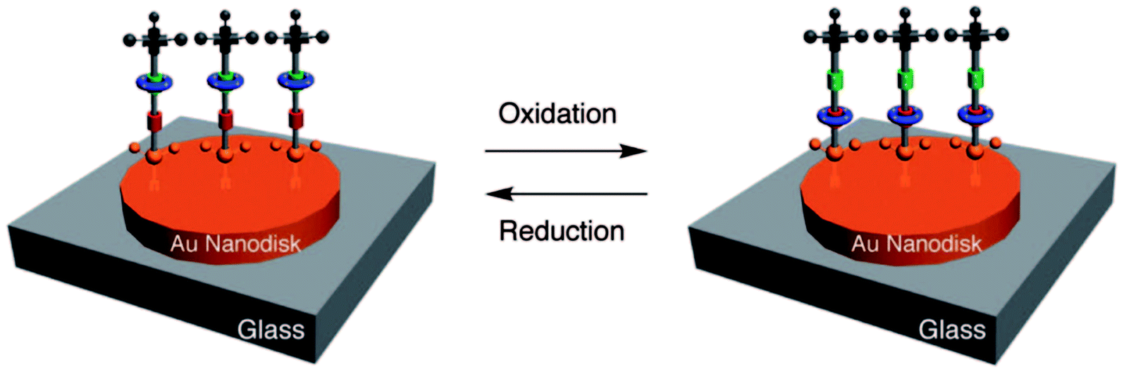 | ||
| Fig. 11 Working principle of the molecular-machine-based active plasmonics107 (printed with permission from ref. 107, Copyright © 2009, American Chemical Society). | ||
The fabrication process of the [2]rotaxane-Au nanodisk array mainly involves lithography and reactive ion etching (RIE). The processing steps are summarized as follows.107
(1) First, a thin chromium (Cr) layer was evaporated on a glass substrate.
(2) Then, a Au thin film with a certain thickness was evaporated on the glass substrate. The Cr layer was sandwiched between the Au film and the glass substrate for enhancing the adhesion of the Au film on the glass substrate.
(3) A self-assembled monolayer of close-packed polystyrene (PS) nanospheres was deposited on the Au surface.
(4) O2 RIE was performed to transform the monolayer of close-packed PS nanospheres into a separated nano-elliptical array;
(5) Ar RIE was performed to selectively etch the parts of the Au and Cr films that are not protected by the nano-ellipses;
(6) Ultrasound was used to remove PS in toluene, and an ordered Au nanodisk was left on the glass substrate;
(7) The [2]rotaxane monolayer was finally formed on the nanodisk by incubating the Au nanodisk in a specific [2]rotaxane solution for 2 days.
The size of a gold nanodisk: diameter: 140 nm; thickness: 17 nm.
The size of a cylindrical glass substrate: diameter: 140 nm; thickness: 45 nm.
The size of a Cr layer: diameter: 140 nm; thickness: 3 nm.
The STM image of another disk-like molecular memory discussed in Section 3.1.1 is shown in Fig. 12.93 As a typical disk-like molecular memory, it uses STM as a movable probe to read and write [2]rotaxane molecules on the substrate. There were two substrates involved in the experiment. First, the [2]rotaxane film was transferred onto an ITO – coated glass substrate using a common LB deposition technique. The substrate was dipped and lifted in the [2]rotaxane solution 50 times to complete the [2]rotaxane coating. The average thickness of a [2]rotaxane LB film was about 70 nm. The second substrate was pure HOPG. A [2]rotaxane LB film of about 20 nm thickness was deposited on an HOPG substrate. The [2]rotaxane recording dots showed reversible operation in the [2]rotaxane/ITO case; however, the easing operation failed in the [2]rotaxane/HOPG case.
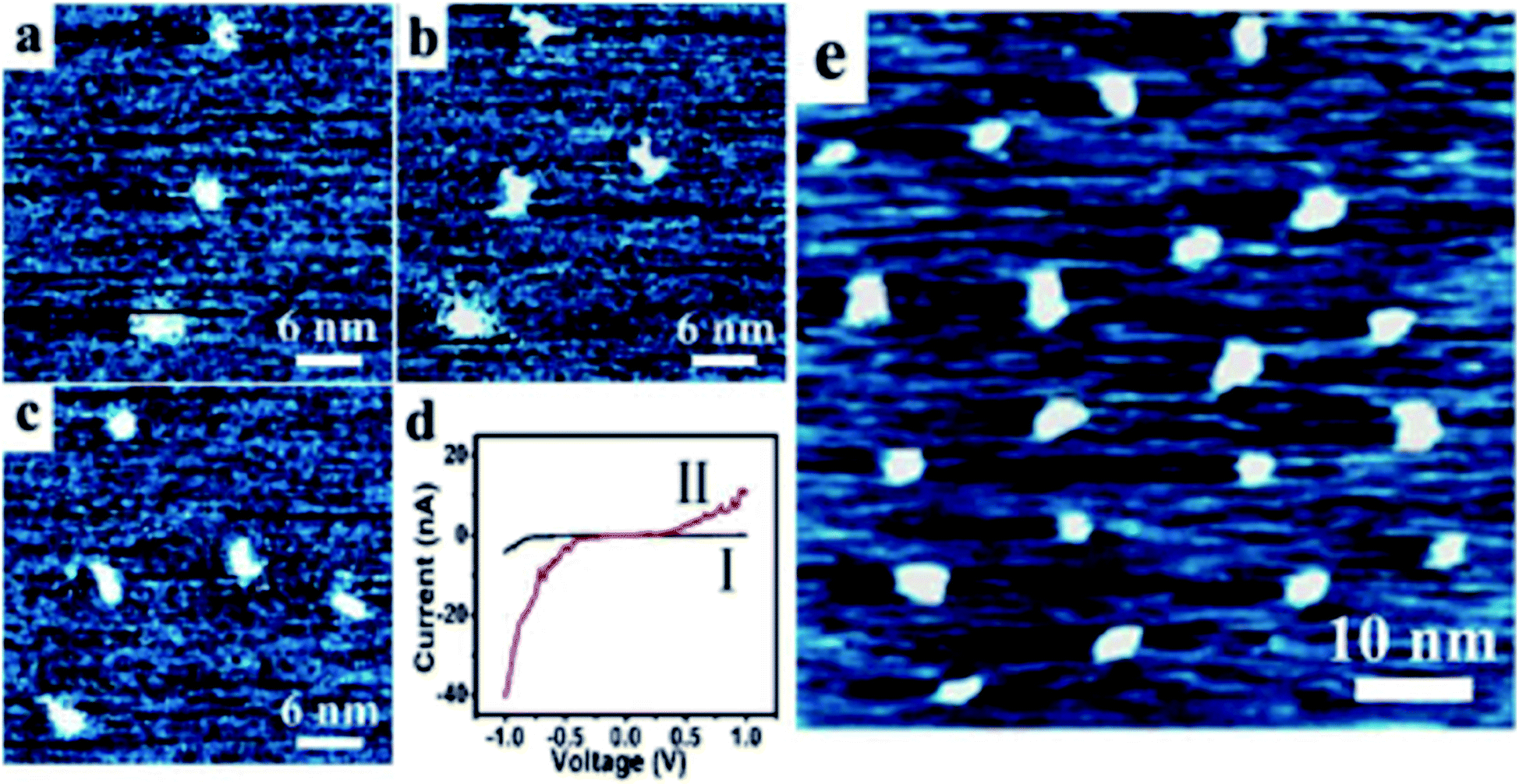 | ||
| Fig. 12 STM images of the recording dots written on the H1 thin films. (a–c) Recording dots written one by one through the application of the voltage pulses from the STM tip. (d) Typical I–V characteristics measured on the original films (I) and on the induced recording dots (II). (e) STM images of a 5 × 4 recording dot array on the H1/HOPG sample. This film has been left exposed to air for about 2 months since its preparation. STM was performed in constant current mode with set points of (Vbias) 0.65 V and (Iref) 0.05 nA (ref. 93) (printed with permission from ref. 93, Copyright © 2005, American Chemical Society). | ||
Similarly, Ye, et al.110 anchored the bistable [2]rotaxane molecule laterally on the Au surface. The molecular switching was electrochemically controlled by using STM. The structure and motion of a bistable rotaxane molecule are shown in Fig. 13. The fabrication process includes two steps. After the [2]rotaxane molecule was synthesized, a Au{111} single crystal disk was cleaned and prepared. Then, the [2]rotaxane molecule was transferred onto a Au{111} disk surface by putting it in the [2]rotaxane·4PF6 solution for 10–20 s immersion.
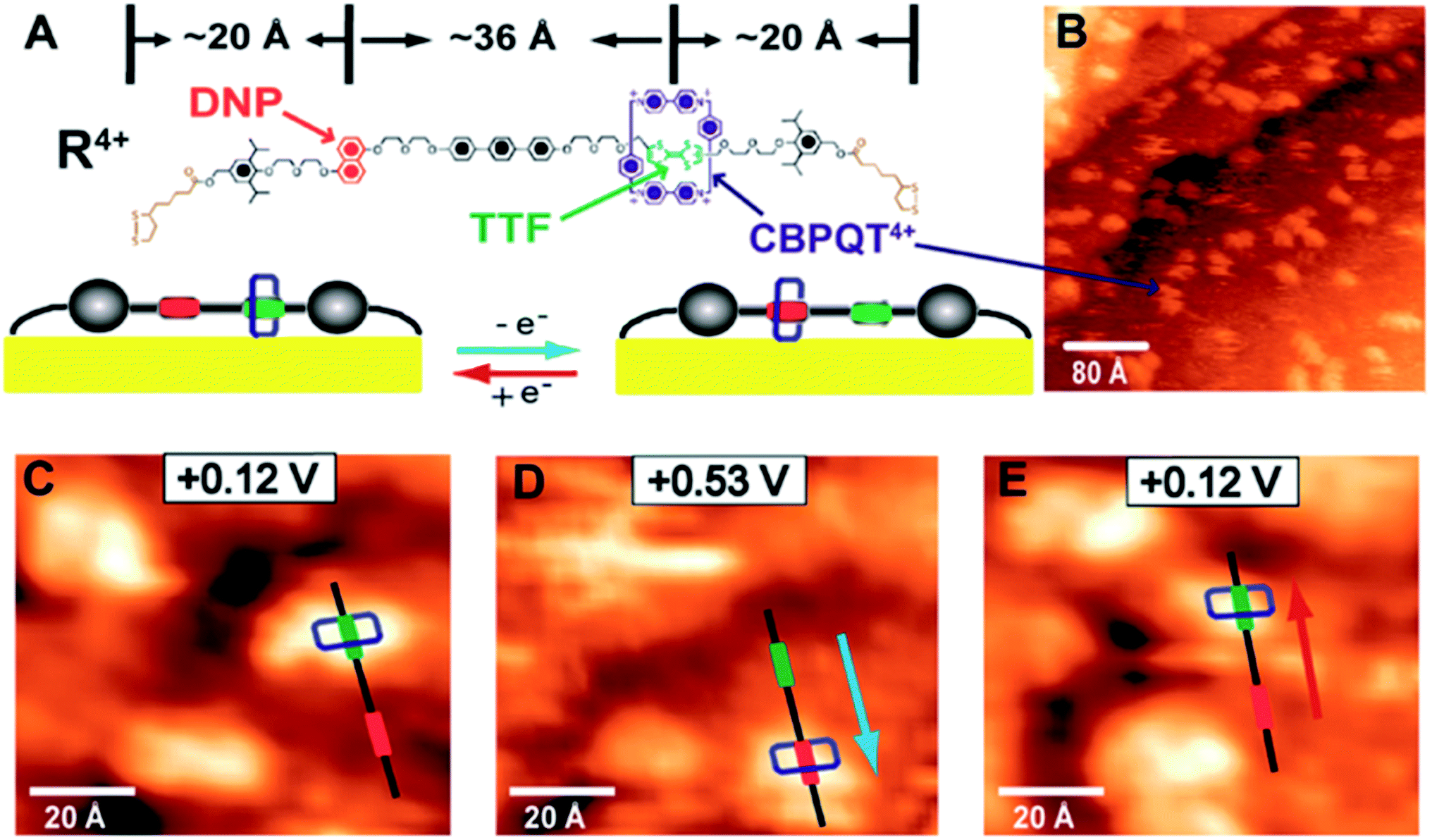 | ||
| Fig. 13 Structure and motion of a bistable rotaxane molecule, adsorbed on Au{111} investigated using electrochemical scanning tunneling microscopy. (A) The tetracationic cyclobis(paraquat-p-phenylene) ring (CBPQT4+, blue) is known to move along the thread between two recognition sites (tetrathiafulvalene, TTF, green and 1,5-dioxynaphthalene, DNP, red stations) depending on the redox state of the TTF unit. (B) The protrusions are assigned to CBPQT4+ rings. (C) In its reduced state at +0.12 V, the CBPQT4+ ring prefers to encircle the TTF station. (D) Upon oxidation (+0.12 to +0.53 V) of the TTF station into a radical cation, electrostatic repulsion propels the ring to the DNP station (blue arrow). (E) Upon reduction (+0.53 to +0.12 V) of the TTF station to neutrality, the metastable state of the bistable rotaxane relaxes back to its thermodynamically favorable state, wherein the CBPQT4+ ring occupies the TTF station (red arrow). Image conditions: Vbias = 0.3 V; Itunneling = 2 pA. The faradaic current was typically less than 10 pA (ref. 110) (printed with permission from ref. 110, Copyright © 2010, American Chemical Society). | ||
5.3 Transistor-like structure
There are two typical [2]rotaxane molecular transistors. The first type uses [2]rotaxane as a single molecular transistor. One example is shown in Fig. 14 and 15.78,125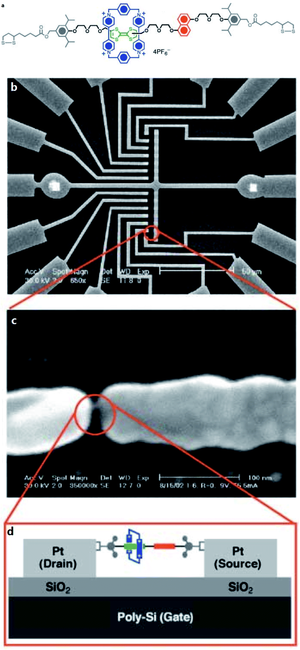 | ||
| Fig. 14 (a) Molecular structure of the bistable [2]rotaxane. The [2]rotaxane has CBPQT4+ (dark blue) as the ring component and the supporting counterions are hexafluorophosphate. (b) Scanning electron microscope (SEM) pictures of single molecule devices fabricated on a Si substrate. A 30 nm thick low-temperature thermal oxide of Si was grown on top of a degenerately doped Si substrate. The center metal electrode, where the break junction is made of 7 nm thick Pt, followed by 100 nm thick gold wires and pads for wire bonding. (c) The SEM image after the break junction is made. The separation between the two metal electrodes is around 4 nm. (d) A section through a single-molecule transistor78 (printed with permission from ref. 78, Copyright © 2003, WILEY-VCH Verlag GmbH & Co. KGaA, Weinheim). | ||
In the other type of [2]rotaxane molecular transistor, the [2]rotaxane molecule is not directly used as a single molecular transistor. Instead, the electron transfer during the switching of the [2]rotaxane molecule will change the conductance of the channel between the source and drain (Fig. 7). So, the transistor will be ON or OFF according to the state of the [2]rotaxane molecules. The previous case125 in Session 3.2.1 is an example of this type. Fig. 15 shows the optical image of the example and its microfluidic system.125
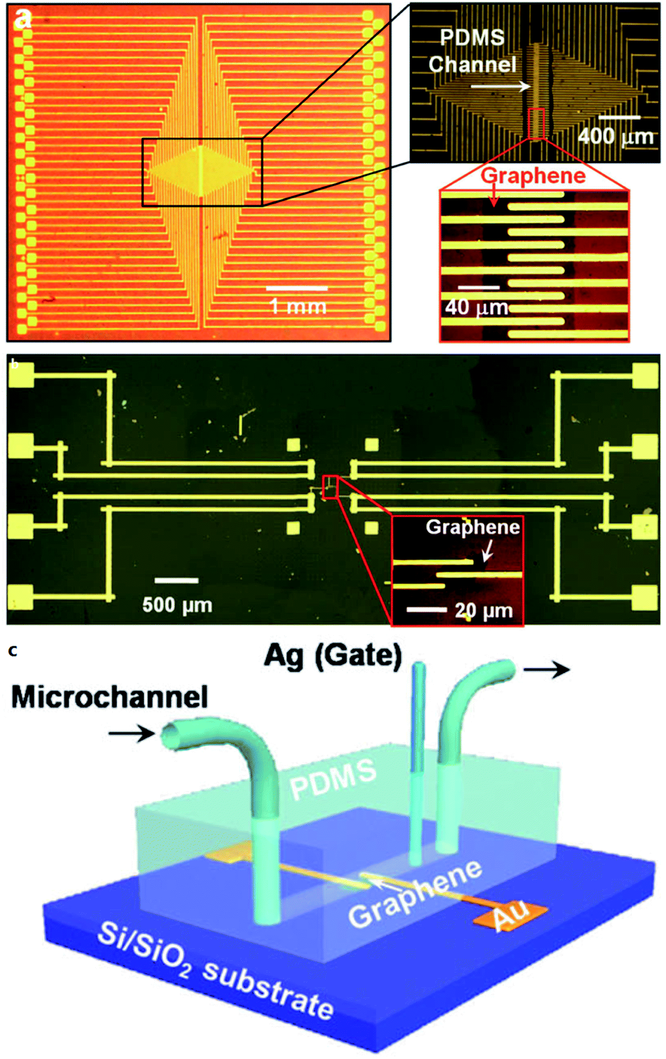 | ||
| Fig. 15 (a) An optical image of a high-density graphene transistor array. The insets show the enlarged optical images of the central parts with microfluidics as marked, respectively. (b) An optical image of a device using pristine graphene formed by a peeling-off technique. Inset shows the enlarged optical image of the central part as indicated. (c) Schematic representation of the experimental setup which integrates a solution gate through an Ag wire as the reference electrode into the microfluidic system125 (printed with permission from ref. 125, Copyright © 2013, WILEY-VCH Verlag GmbH & Co. KGaA, Weinheim). | ||
The fabrication details of the high-density graphene transistor array:125
(0) Microfluidic system preparation. Firstly, soft lithography and replica molding techniques were performed to form 100 μm × 250 μm PDMS microfluidic channels. Then, the [2]rotaxane decorated graphene was lithographically fabricated on a silicon/SiO2 substrate. Finally, the PDMS stamps were transferred precisely onto top of the resultant silicon wafers.
(1) The [2]rotaxane molecule and the linker were obtained by chemical synthesis.
(2) High-quality single-layer graphene (SLG) was obtained by a low-pressure chemical vapor deposition (CVD) method.
(3) SLG was transferred to a Si/SiO2 substrate by using a non-destructive PMmaMediated method and wet-etching technology.
(4) The graphene sheet was obtained by using a photolithographically patterned resist mask with selective oxygen plasma etching.
(5) The source electrode and drain electrode were formed on the graphene transistor array by photolithography and thermal evaporation.
(6) The silicon oxide passivation layer of each photolithography step was completed by electron beam thermal evaporation.
(7) The [2]rotaxane molecule was assembled on a graphene surface via a PBA linker to form a molecular array.
(8) The PDMS microfluidic channels were manufactured by using soft lithography and replica molding technology. The channels were used to control the solution environment (solvent or air) and control the light path (introducing a light or dark environment).
5.4 Crossbar architecture for molecular switch tunnel junctions
The crossbar structure is a nanometer-scale cross-over switch system, consisting of two sets of parallel nanowires vertically distributed on the upper and lower layers. The middle layer is composed of switches linking the upper and lower cross points. The structure is shown in the figure below. The three-layer structure of the Crossbar shown in the picture is very similar to a sandwich. Each node is an independent switch unit, operating through the upper and lower two nanowires linked by it. For example, using this structure as a memory, by controlling the voltage of the two electrode nanowires, the switch can be “written”, “read” or “erased”.Fig. 16 shows a 4 × 4 storage structure as an example. 4 × 4 means that there are four nanowires at the top (denoted as Y0, Y1, Y2, and Y3, respectively), and four nanowires at the bottom (denoted as X0, X1, X2, and X3 respectively). Sixteen intersections are formed between the two interlaced nanowires. Each intersection is linked with a switch, acting as a memory cell, with a total of four cells (denoted as C0–C15). Each unit can be addressed in 2-dimensional coordinates and perform “write” operations. Then, it performs “read” operation by addressing Cn(Xn, Yn). In this way, this 4 × 4 crossbar structure becomes a 16 bit memory. Similarly, if it is expanded to N × N, there will be N2 memory cells. To address a single unit, only Ci(Xi, Yi) needs to be determined. In addition to storage, the crossbar structure can also be used to build logic circuits.
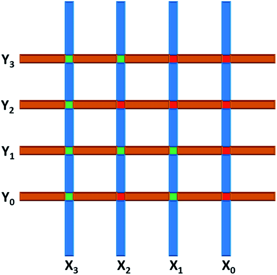 | ||
| Fig. 16 A 4 × 4 crossbar storage structure (red – “0”; green – “1”). | ||
For [2]rotaxane molecular circuits, there are two possible device architectures in two dimensions in Fig. 17. The honeycomb architecture may potentially be applied for [2]rotaxane transistors, while the crossbar architecture may potentially be applied for memory and reprogrammable logic arrays.
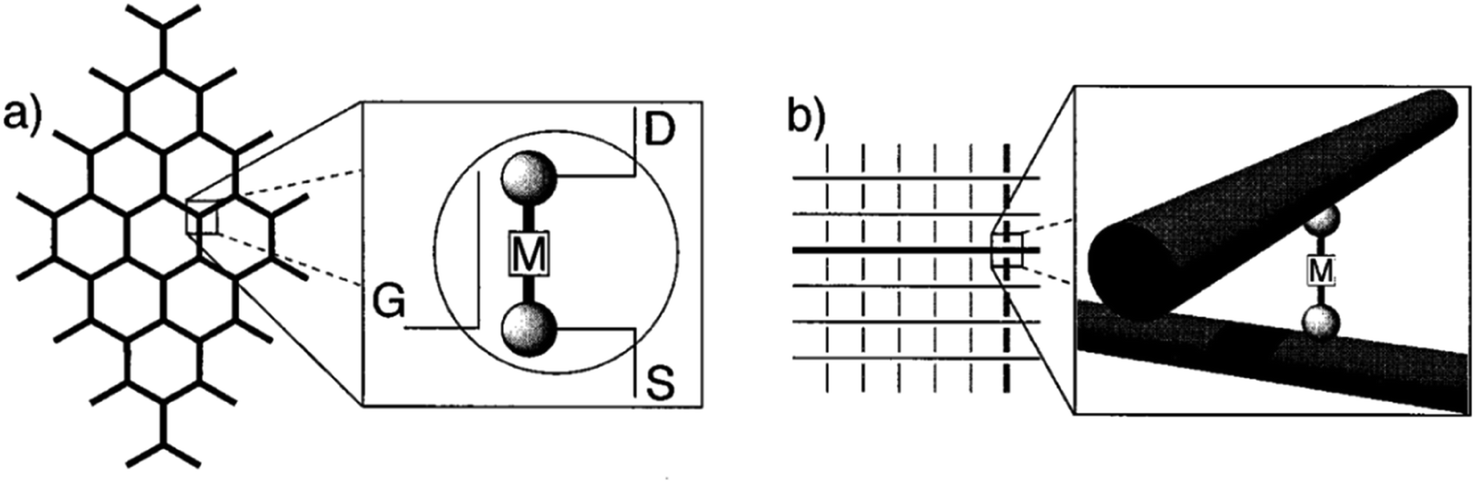 | ||
| Fig. 17 (a) Three-terminal devices (transistors) arranged in a hexagonal lattice; (b) two-terminal devices arranged in a square lattice or crossbar structure. Note that there is no way to access an embedded three-terminal device without electrically addressing surrounding devices. However, an appropriate bias on a horizontal wire and a vertical wire can be used to access an embedded two terminal device. Note that G, S, and D represent the gate, source, and drain terminals of a field effect transistor; M stands for a molecule70 (printed with permission from ref. 70, Copyright © 2001, American Chemical Society). | ||
5.5 Crossbar: metal–molecule–metal sandwiched structure
If we take a look at one junction in the crossbar, it is actually a sandwiched structure. The [2]rotaxane molecule layer is sandwiched between two metal electrode layers forming a metal–molecule–metal sandwiched structure. One example of junctions is shown in Fig. 18–20.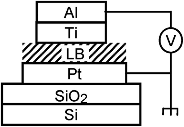 | ||
| Fig. 18 A sandwich structure of 100 nm-Pt/LB monolayer/5 nm-Ti, 200 nm Al79 (printed with permission from ref. 79, Copyright © 2004, American Chemical Society). | ||
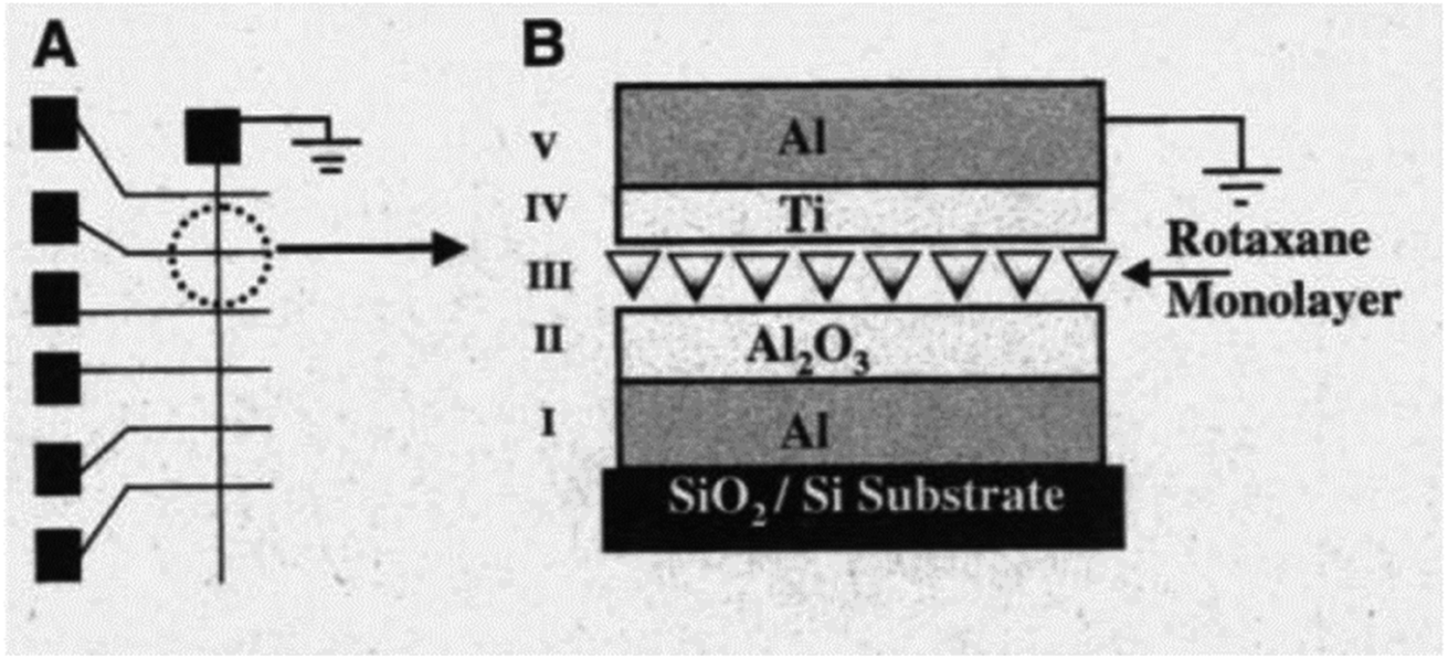 | ||
| Fig. 19 Molecular monolayer devices64 (printed with permission from ref. 64, Copyright © 1999, The American Association for the Advancement of Science). | ||
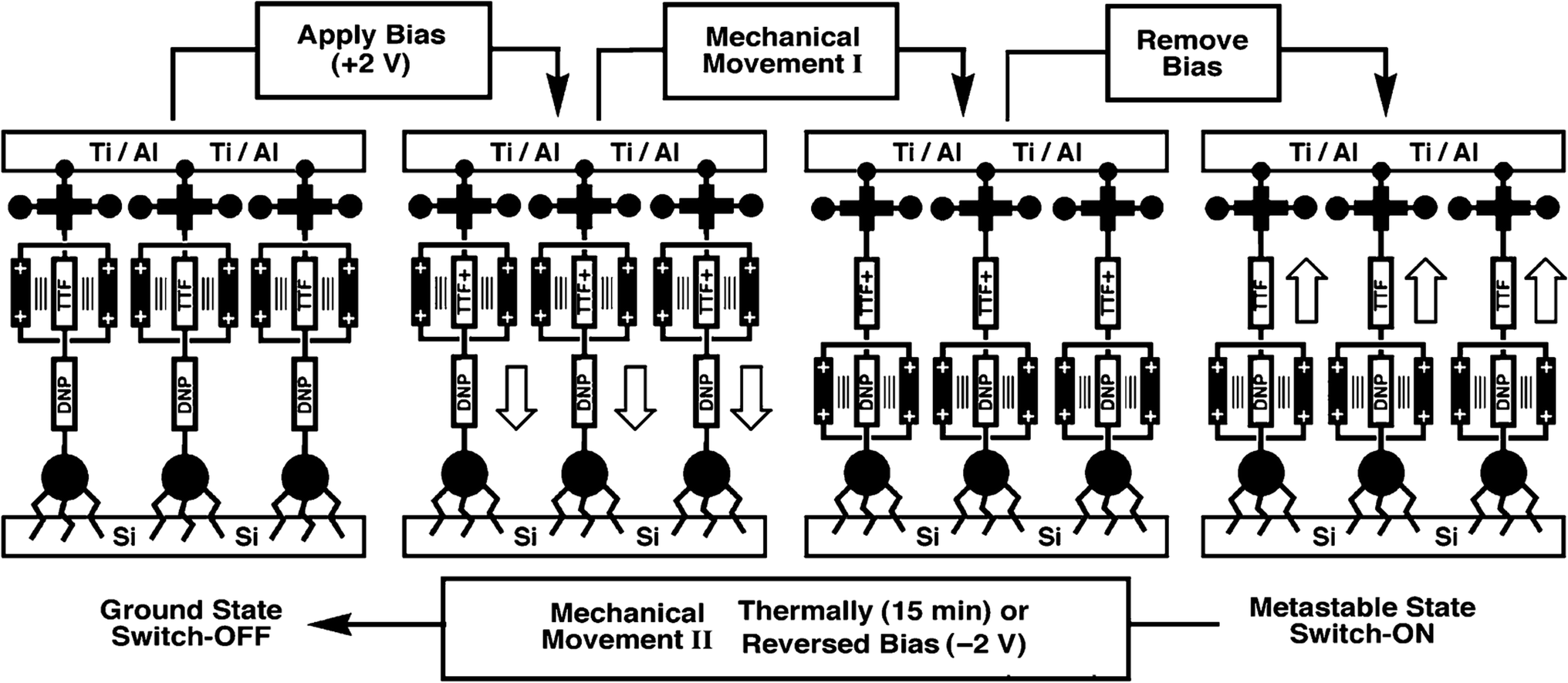 | ||
| Fig. 20 Schematic idealized representation of a molecular switch tunnel junction (MSTJ) composed of a bottom polysilicon electrode, a monolayer of amphiphilic bistable [2]rotaxanes, and a top electrode composed of Ti and Al. The proposed operating mechanism of the device is also shown. Application of +2 V oxidizes the TTF unit and causes movement of the CBPQT4+ ring to the DNP ring system. After the voltage is removed, the TTF unit returns to its neutral form, but the ring remains on the DNP ring system in a metastable state. This state is a higher conducting one relative to the ground state, which is reached when the ring returns to the TTF unit through thermal relaxation or application of −2 V (ref. 85) (printed with permission from ref. 85, Copyright © 2004, WILEY-VCH Verlag GmbH & Co. KGaA, Weinheim). | ||
The main fabrication process of metal–molecule–metal sandwich structures (Fig. 18) includes photolithography and chemical deposition. The bottom electrode layer, the LB monolayer and the top electrode layer were deposited in order on the Si <100> substrate to form 1 × 1 and 3 × 6 crossbar arrays. The “metal–molecular monolayer–metal” structure with two terminals is manufactured as follows:79
(1) The Si <100> substrate was polished.
(2) 200 nm SiO2 was thermally grown on the surface of the substrate.
(3) The bottom electrode of 100 nm platinum (Pt) was formed by photolithography.
(4) The Pt electrode was cleaned with oxygen plasma, which produced a thin surface of platinum oxide of about 0.4 nm.
(5) The LB film was deposited onto the bottom electrode layer, which physically adsorbed on the bottom Pt oxide surface and formed the electrode interface.
(6) After the LB film was deposited, the LB film was masked. Within one hour the top titanium/aluminum electrode layer (5 nm Ti + 200 nm Al) was evaporated by an electron beam.
At the second level, the central issue is how the [2]rotaxane molecular layer is integrated into the circuit and as a part of the electronic component. The above example shows the sandwiched junction structure. Fig. 21–24 introduce the real crossbar strictures and fabrication process by traditional top-down methods.
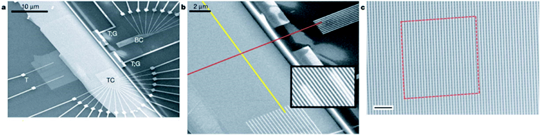 | ||
Fig. 21 SEMs of the nanowire crossbar memory. (a) Image of the entire circuit. The array of 400 Si bottom nanowires is shown as the light grey rectangular patch extending diagonally up from bottom left. The top array of 400 Ti nanowires is covered by the SNAP template of 400 Pt nanowires and extends diagonally down from top left. Testing contacts (T) are for monitoring the electrical properties of the Si nanowires during the fabrication steps. Two of those contacts are also grounding contacts (G) and are used for grounding most of the Si nanowires during the memory evaluation, writing and reading steps. Eighteen electron-beam-lithography patterned top contacts (TC) and ten such bottom contacts (BC) are also visible. The scale bar is 10 mm. (b) An SEM image showing the cross-point of top- (red) and bottom- (yellow) nanowire electrodes. Each cross-point corresponds to an ebit in memory testing. The electron-beam-lithography defined contacts bridged two to four nanowires each (inset). The scale bar is 2 mm. (c) High-resolution SEM of approximately 2500 junctions out of a 160![[thin space (1/6-em)]](https://www.rsc.org/images/entities/char_2009.gif) 000-junction nanowire crossbar circuit. The red square highlights an area of the memory that is equivalent to the number of bits that were tested. The scale bar is 200 nm (ref. 101) (printed with permission from ref. 101, Copyright © 2007, Nature Publishing Group). 000-junction nanowire crossbar circuit. The red square highlights an area of the memory that is equivalent to the number of bits that were tested. The scale bar is 200 nm (ref. 101) (printed with permission from ref. 101, Copyright © 2007, Nature Publishing Group). | ||
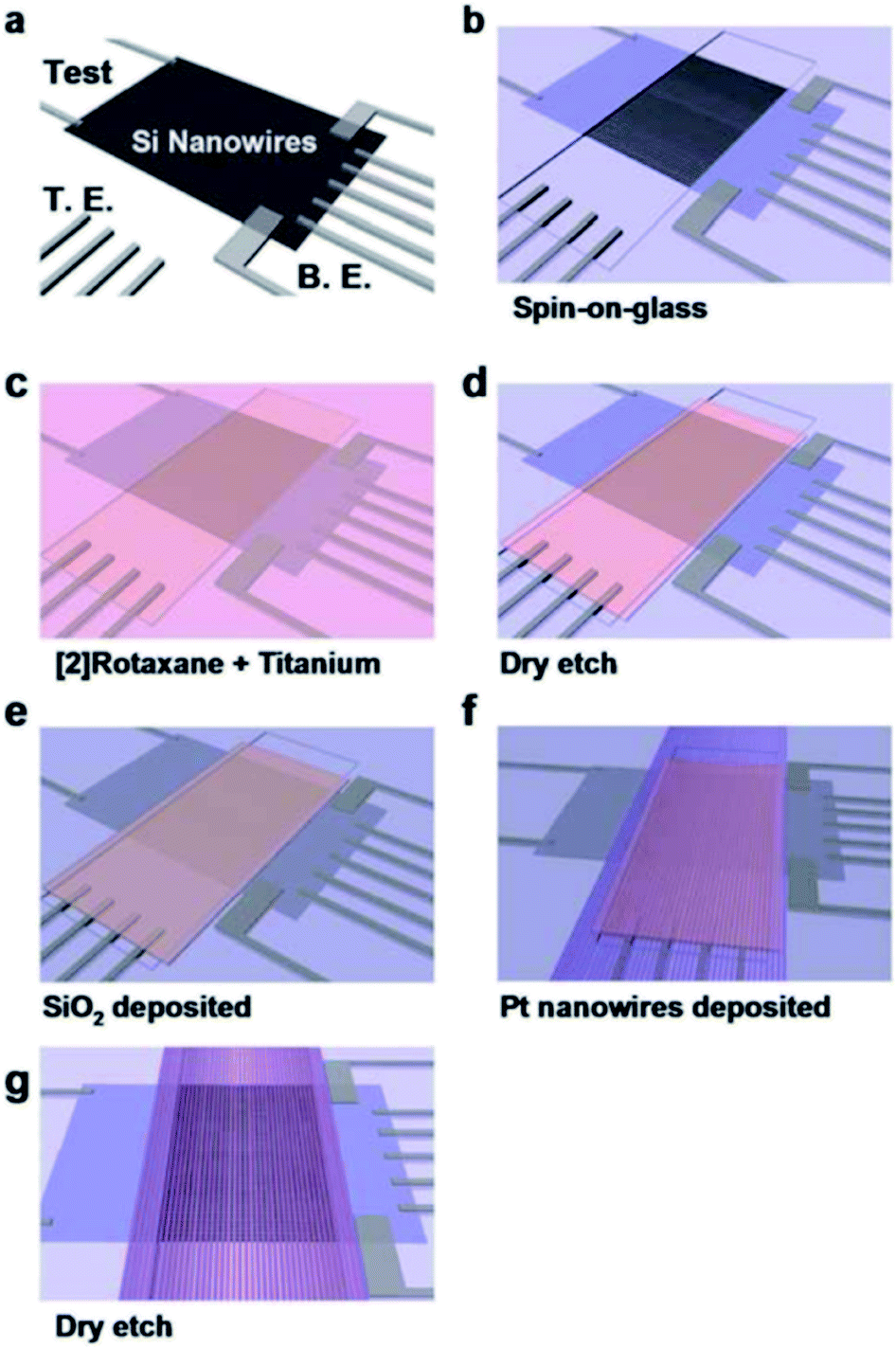 | ||
| Fig. 22 Process flow for preparing the 160 kbit molecular electronic memory circuit at 1011 bits per cm2 [in ESI of ref. 101 ] (printed with permission from ref. 101, Copyright © 2007, Nature Publishing Group). | ||
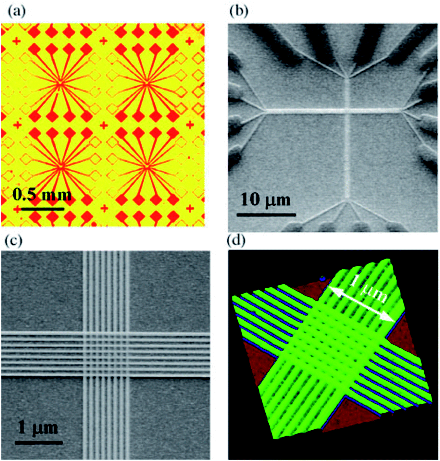 | ||
| Fig. 23 (a) An optical microscope image of an array of four out of 625 test circuits, showing that each has 16 contact pads with micron-scale connections leading to nanoscale circuits in the center. (b) An SEM image showing two mutually perpendicular arrays of nanowires connected to their micron-scale connections; (c) an SEM image showing that the two sets of nanowires cross each other in the central area; (d) a 3D AFM image of the crossbar81 (printed with permission from ref. 81, Copyright © 2003, IOP Publishing). | ||
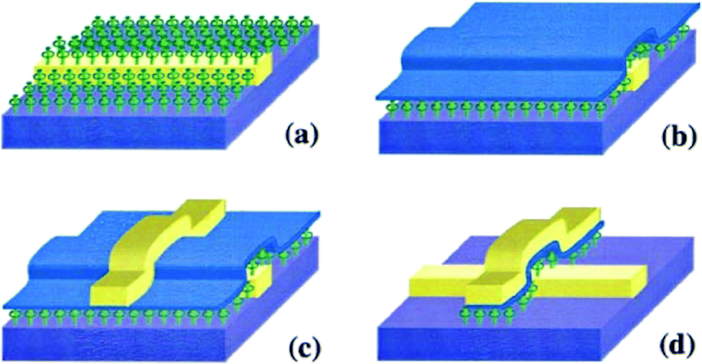 | ||
| Fig. 24 Schematic of the procedure used for the fabrication of nanoscale molecular-switch devices by imprint lithography80 (printed with permission from ref. 80, Copyright © 2003, AIP Publishing). | ||
The core part of the process for preparing the 160 kbit molecular electronic memory circuit is Superlattice Nanowire Pattern Transfer (SNAP). The main flow is shown as follows.
(1) Si nanowires were prepared by SNAP to form the bottom electrode layer, which was contacted with the metal electrodes.
(2) The spin-on-glass (SoG) method was used for the circuit and photolithographic patterning was used, followed by dry etching, to expose the active memory area.
(3) The [2]rotaxane LB film was deposited on top of the Si nanowire electrode layer, and it was protected by depositing a thin Ti layer.
(4) The active memory area was kept and the extra molecule/Ti layer was removed.
(5) SiO2 insulator was deposited on top of the Ti film.
(6) The SNAP was used again for depositing the top Pt nanowire array, which was perpendicular to the bottom Si nanowires.
(7) Dry etching was performed for transferring the Pt nanowire pattern to the Ti layer to form the top Ti nanowire electrode array and the crossbar structure was completed.
The main fabrication process of the [2]rotaxane molecular is shown in Fig. 24.80
(1) Electron beam lithography and reactive ion etching (RIE) were used to manufacture silicon oxide molds with three-dimensional bottom patterns.
(2) The pattern (three-dimensional structure) from the mold is transferred to the PMMA film on the substrate by nano-imprinting. After imprinting, excess PMMA was removed by RIE.
(3) A thin layer of Ti was formed on the PMMA pattern by chemical deposition, and then a layer of platinum was deposited (the bottom titanium/platinum nanoelectrode layer was formed).
(4) Using a chemical lift-off method, the non-patterned structure was removed; only the titanium/platinum nanoelectrode wires and contacts were left on the substrate. A LB film was used to transport [2]rotaxane, so that the [2]rotaxane monolayer was deposited on the bottom electrode layer.
(5) Similar to step 3, the top titanium/platinum nanoelectrode layer was formed by chemical deposition. Non-structural parts were removed by RIE, and finally a “Ti/Pt-[2]rotaxane-Ti/Pt” three-layer crossbar structure was formed on the substrate.
6 The level 3 challenge: integration at the system level, crossbar and supramolecular rotaxanes
Finally, as mentioned earlier, molecular circuits are still facing difficulties in the current development. Most research on rotaxane is focused on the application of molecular machines. The work of our research first focuses on examining [2]rotaxanes from the perspective of electronics rather than molecular machines, and at the level 1 phase, we study the switching characteristics of [2]rotaxanes via simulations and experiments. Second, at the level 2 phase, we study the characteristics of the interface between [2]rotaxanes and the electrode layer, especially the use of novel nanomaterials such as graphene and carbon nanotubes as the electrode interface. Third, we construct molecular circuits by using crossbar structures and study the feasibility of supramolecular structure applications in [2]rotaxane circuits. Additionally, there are few discussions on the optimization of designing [2]rotaxane molecule circuits. For example, as a memory junction, what should be the minimum distance for [2]rotaxane molecules to work properly in a memory array without significant interference and crosstalk? This would decide the minimum pitch of [2]rotaxane moletronics. Furthermore, a design rule checking (DRC) mechanism for [2]rotaxane moletronics analogous to the design rule checking (DRC) in microelectronics is also proposed to tolerate process variations in layout design.Before trying to resolve the third level of challenges, the challenges of the first two levels of the pyramid must been thoroughly addressed. Ensuring the functional characteristics of [2]rotaxane switches, the third level is concerned with the realization of logic functions, and then system-level controlling and communication. The following classic example (in Fig. 25 and 26) describes a crossbar structure of 64 bit random-access memory. The device can realize the demultiplexer (multiplexer) function by addressing the stored truth table values in it. This is the feature of the crossbar structure and the basic function of a logic circuit is realized by dividing the area into an addressing circuit part (decoder) and an outputting logic results (memory). Another example, as shown in Fig. 27, demonstrates how to use the crossbar structure to implement a 1-bit full adder.
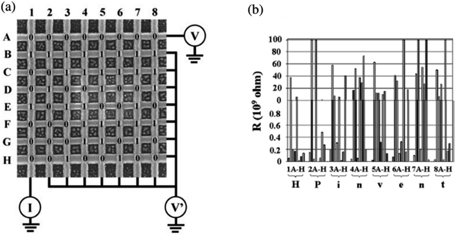 | ||
| Fig. 25 The crossbar as a 64 bit random access memory. (a) The ideal ‘write’ and ‘read’ modes for the memory. To write a bit, V is increased in increments of 0.5 from 3.5 V until the bit is written or V reaches 7 V, while keeping V′ = V/2 (in our actual circuit, the vertical nanowires were floating); to read a bit, V = 0.5, and V′ = 0. (b) Resistance at each cross point in the circuit after one particular set of bits was written into a defect-free crossbar. The resistances of the cross points representing ‘0’ states, which ranged between 106 and 5 × 10⁸ Ω, are shown in the bottom half of the plot; the resistances of the cross points representing ‘1’ states, which are >4 × 10⁹ Ω, are shown in the top half of the diagram. The bit state at each cross point is indicated by a ‘0’ or ‘1’ in figure (a). Each column corresponds to a standard ASCII character, and the bits stored in the memory represent the characters ‘HPinvent’81 (printed with permission from ref. 81, Copyright © 2003, IOP Publishing). | ||
 | ||
Fig. 26 The crossbar as a combination of a 4 × 4 demultiplexer (top right), a 4 × 4 memory (bottom right) and a 4 × 4 multiplexer (bottom left). The black squares in the de/multiplexer sections show the positions of the low-resistance cross points, and the rest of the cross points have a high resistance. The nanowires A–D (1–4) are used as addressing wires with their voltages being set externally by Va and Vb(V1 and V2) through ‘identity’ and ‘not’ gates, which in turn determine the DC voltages on nanowires 5–8 (E–H). The external circuit on the top right (bottom left) functions as part of the demultiplexer (multiplexer) to selectively apply (detect) an AC signal on one and only one of the nanowires among 5–8 (E–H) to ‘read’ the resistance at the cross point of the two selected nanowires. In the circuit, Ṽ1 = 0.25 V (100 Hz), ![[V with combining macron]](https://www.rsc.org/images/entities/i_char_0056_0304.gif) 1, 2 = 1.0 V, Cac1, Cac2 = 1 μF, Rdc1, Rdc2 = 50 MΩ, C5–8 = 0.5 nF and CE–F = 100 pF. Va, Vb, V1 and V2 are set to 0.0 or 2.0 V. Ã represents an AC meter81 (printed with permission from ref. 81, Copyright © 2003, IOP Publishing). 1, 2 = 1.0 V, Cac1, Cac2 = 1 μF, Rdc1, Rdc2 = 50 MΩ, C5–8 = 0.5 nF and CE–F = 100 pF. Va, Vb, V1 and V2 are set to 0.0 or 2.0 V. Ã represents an AC meter81 (printed with permission from ref. 81, Copyright © 2003, IOP Publishing). | ||
 | ||
| Fig. 27 Implementation of a one-bit full adder (a). Fast Boolean Logic Circuits – FBLC (b). Optimized Fast Boolean Logic Circuits – OFBLC173 (printed with permission from ref. 173, Copyright © 2015, IEEE). | ||
As a very promising architecture for molecular electronics, the nanowire crossbar system has several advantages. Compared with the complex structure of silicon-based processors, the crisscrossed nanowires make manufacturing relatively simple. Interleaved arrays provide a convenient way to implement row/column redundancy and fault tolerance. Molecular electronics generally has high defect density in the manufacturing process. The crossbar architecture is similar to the memory array architecture; hence it can easily borrow the strategy of fault tolerance and redundancy repair from memory. If any molecular switch fails, you can easily switch it off and replace it with redundant rows and columns. This is essential for the molecular memory circuit to work normally even if some of the molecular switches are defective. Crossbar's single geometric shape can provide storage, logic, and interconnection functions, with high adaptability. Each unit can be reconfigured, which makes the crossbar system have more application scenarios in random access memory or field programmable logic circuits. At the same time, it is a non-blocking network that can realize multiple I/O connections at the same time and provide a complete connection, which maximizes the bandwidth usage.
There are several factors affecting the bit density of a molecular circuit with a crossbar structure. First, to ensure data reliability, the signal interference and crosstalk between neighboring molecules must be considered in deciding the minimum pitch of moletronic circuits. Second, the size and spacing of the nanowires are also limited by available fabrication technologies including top-down and bottom-up fabrication processes. Furthermore, even moletronics can theoretically achieve extremely high device density, and the signals from moletronics eventually need to be connected to the external world. Each nanowire inside moletronics needs to be individually controllable and addressable from external microelectronic circuitry, which has a relatively wider line width. This also brings about a limit to the maximum bit density of the moletronic blocks. For a long period of time, moletronics may need to co-exist with conventional microelectronics in a single chip. Thus a proper interface between moletronics and microelectronics needs to be designed so that the signal can travel seamlessly back and forth between both domains. Such interface circuitry acts as a “bridge” to connect moletronic and microelectronic building blocks. To alleviate the limitation imposed by external connection, a possible efficient scheme to connect the nanowires of the crossbar circuit and the external microelectronic circuit is through the decoder and multiplexer/demultiplexer circuitry.174,175 The decoders would allow using a smaller number of external mesowires to access ultra-high density nanowires inside the moletronic blocks. Since the nanowire crossbar circuitry has inherent high variability and defect-tolerance capability, it requires the decoders to be designed with innovative defect-tolerance methods, and to be compatible with the nanoscale features of nanowires. For example, DeHon, et al.174 devised a hybrid decoder design. Even if the size of the decoder increases, it does not require any growth of the size of unique codes for the nanowires. Besides, the device is able to tolerate gross misalignment of interfaced microwires and still retain independent addressability. The scheme provides an efficient solution for bridging the gap between nanoscale and microscale features and guides the programming and customizing of the system at the nanoscale level. As another example, Jamaa, et al.175 designed a Gray-code-based decoder with a 17% reduction in fabrication complexity and a 51% reduction of the effective bit area. Fig. 28 shows an example of using the decoder circuit to connect the crossbar circuit and the external CMOS circuit. With the decoder, each nanowire of the crossbar circuit can be uniquely addressed by an external circuit through the applied voltage pattern.
 | ||
| Fig. 28 The decoder circuit connection example. (a) Baseline architecture of a crossbar circuit and (b) highlights of the decoder layout (c) circuit175 (printed with permission from ref. 175, Copyright © 2009, IEEE). | ||
At the system level, it is a visible trend that the crossbar structure could be a universal architecture to construct logical modules, memory modules and other related communication modules (e.g. sensors, actuators, thermoelectronics, optoelectronics, etc.) to achieve systemic functions on a single chip (System-on-a-Chip). As an example, Fig. 29 shows the strategy of integration of various nanoelectronic circuits with multiplexers. Communications between the functional circuit blocks are controlled and regulated via reconfigurable multiplexers. Those functional circuits can be CMOS circuits or molecular-based nanowire crossbar circuits. This strategy, at the system level, is a typical CMOL (CMOS/MOLecular hybrid) circuit that is compatible with both conventional and non-conventional circuits and finally expands the boundaries of conventional circuits. Additionally, with the increase of the field programmable gate array (FPGA) based on lookup tables, the application of crossbar structures to build FPGA-like systems will become a very attractive topic in the future. It is conceivable that the future molecular circuit systems, with a high throughput, reprogrammability, and the ability to switch between memory and logic, will further expand the application scenarios of moletronics.
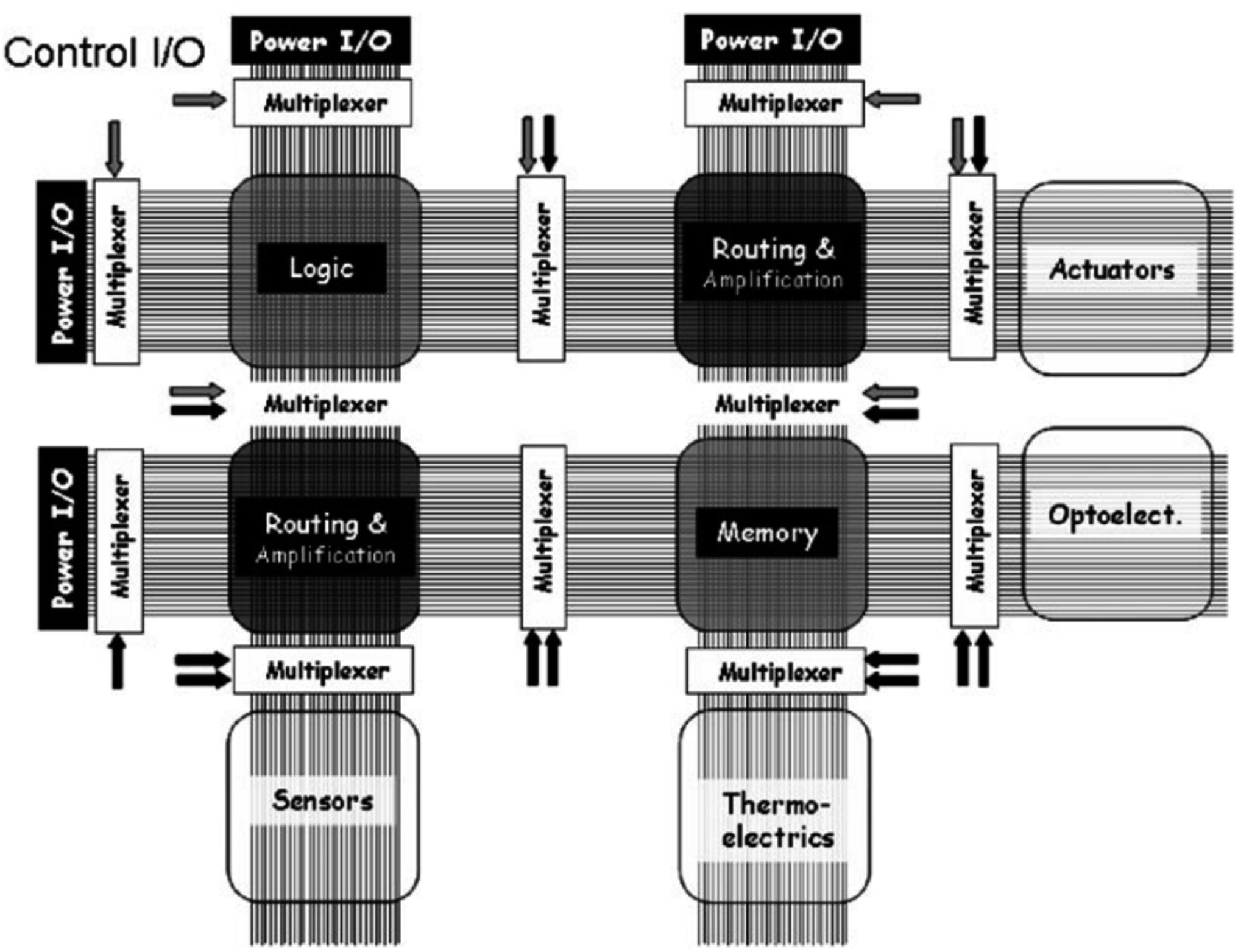 | ||
| Fig. 29 A molecular and nanoelectronic computational platform based upon a patchwork of crossbar structures. Various traditional and non-traditional functions are illustrated, with multiplexers (and demultiplexers) controlling communication between the various functions and input/output (I/O) with the outside world. This particular circuit architecture is defect tolerant and amenable to both traditional and non-traditional patterning methods92 (printed with permission from ref. 92, Copyright © 2006, Royal Society of Chemistry). | ||
In this review, [2]rotaxane is the main subject of discussion. However, rotaxane is a large diversified family and there are many other members available. In addition to [2]rotaxane, supramolecularly structured polyrotaxanes and rotaxane dendrimers also show potential for applications in moletronics. As a supramolecular structure, polyrotaxane is a mechanically interlocked molecule like [2]rotaxane but with multiple rings (macrocycles). Such a long chain structure with multiple rings could potentially be utilized to implement an inverter chain for moletronics applications. Due to its longer chain length and higher number of macrocycles, the mechanical properties of polyrotaxane are different from [2]rotaxanes, which brings about their own unique opportunities and possibilities. For example, the flexibility and ductility of polyrotaxanes allow them to be used as smart polymer binders for battery electrodes. One major issue in lithium-ion batteries is the insufficient cycle life of negative silicon electrodes due to the fact that the volume of silicon changes dramatically during repeated charge–discharge cycles. As a recent example, Choi, et al.137 pointed out that stress dissipation during silicon volume expansion is the key to improve the robustness of silicon anodes. A ring-slide polyrotaxane as a polymer binder was utilized in their work. Due to the sliding action of macrocycles along the polyrotaxane, the tension exerted on the polymer network was significantly reduced, making the prepared polymer network highly stretchable and elastic. Even pulverized silicon particles will be coalesced without disintegration during repeated (de)lithiation, and thus the cycle life of the silicon anode was greatly extended. The significance of this example is that a similar approach can help increase the content of the dopant such as silicon in the electrode, which can potentially increase the energy density at the molecule–electrode interface. This shows positive implications for the research and development of molecule–electrode interfaces.
Moreover, [2]rotaxane is mainly used in solid-state circuit devices, which requires [2]rotaxane films or other forms to be integrated between solid-state electrode layers. However, electrically responsive polyrotaxane can be applied to flexible circuits and flexible memory devices as well. Zhou, et al.165 synthesized a conjugated polyrotaxane (CPR1) for high-performance non-volatile resistive random-access memory (RRAM) devices. The resistance switching is realized by a reversible electric-field-induced proton doping/de-doping of the threading polyaniline core with a β-CD macrocycle sheath through hydrogen bonding interactions. The device featured a high ON/OFF ratio of 108, a fast response time of 29 ns, an excellent reliability and repeatability, and a long-term stability that lasted more than one year. In particular, the conjugated polyrotaxane showed a good solubility and flexibility. This hints that large-scale flexible RRAM device arrays can be efficiently fabricated by using an energy-efficient full-printing technique at a low cost. The fully printed RRAM array shows excellent device yield, and each cell of the array is separated, effectively avoiding crosstalk between cells. Compared with small molecular rotaxanes, polyrotaxanes have considerable advantages in terms of synthetic efficiency and ease of manufacturing.
In addition to applying the crossbar structure to build future molecular circuits, including both memory and logic circuits, the supramolecular rotaxane structure is also worthy of attention. Rotaxane dendrimers are a large family of mechanically interlocked molecules (MIMs) with a hyperbranched structure which also demonstrate effective molecular switching properties. Up to now, the preparation of functional rotaxane branched dendrimers has always been one of the most attractive topics in supramolecular chemistry, but the synthesis of its supramolecular structure has always been extremely challenging. Dendrimers are mainly synthesized by two methods: divergent approach and convergent approach. In a divergent approach, the synthesis of dendrimers builds up peripheral branching groups from the core generation by generation. Relatively, a convergent approach builds the core end point starting from the peripheral groups, to form a dendron segment. During recent years, a variety of rotaxane dendrimers have been synthesized and characterized successfully.142,143,150,151,157–159,162 They have precise arrangement of rotaxane units and stimulus-response sites and functional groups. The structure of these rotaxane dendrimers, as shown in Fig. 30–32, has shown great potential in smart nanomaterials, nanoreactors, light energy harvesters, and multifunctional platforms for biological signal transmission.
 | ||
| Fig. 30 Schematic diagram of the growth of type III-B rotaxane dendrimers (T3B-RDs) via a convergent approach142 (printed with permission from ref. 142, Copyright © 2018, The Authors). | ||
 | ||
| Fig. 31 Schematic representation of a controllable divergent approach for the synthesis of rotaxane-branched dendrimers G2 and G3.143 (printed with permission from ref. 143, Copyright © 2018, The Authors). | ||
 | ||
| Fig. 32 Cartoon representations of the three types of rotaxane dendrimers: type I with rotaxane units as cores; type II with rotaxane units as peripheries; type III with rotaxane units as branches162 (printed with permission from ref. 162, Copyright © 2021, American Chemical Society). | ||
At the same time, it also brings about a revelation to molecular electronics, different from the path taken by the crossbar architecture, whether the structure of the rotaxane dendrimer can be used as another path to construct molecular circuits. The switching properties of electrically driven rotaxane dendrimers are worthy of in-depth study. For example, in the type I structure of rotaxane dendrimers, the rotaxane part is used as the core. If each end is connected to an electrode input, it could be used to implement a multiplexer or a majority gate function. Based on multiplexers, any Boolean function can be implemented based on Shannon's expansion. Furthermore, the majority gate can be used to construct an AND/OR gate, and hence it also could lay down the foundation to implement any Boolean logic. The unique multi-branch structure of rotaxane dendrimers could also make them ideal candidates for building multi-input complex Boolean logic gates comparable to complex CMOS gates (e.g. Boolean function Z = [A + (B ∙ C)]', etc.). However, the majority of current studies focus on chemically responsive switching.158 Electrically responsive rotaxane dendrimers, such as the switching properties of the memristive effect, need to be further investigated and explored. Second, some new challenges emerge. How should the end points of the rotaxane dendrimers be linked to electrode layers in circuits? How should the functional molecules be integrated in electronic devices, and what fabrication techniques are required for such structures? All these need to be properly addressed for rotaxane dendrimers to be used for moletronic circuits. Finally, at the system level, the molecular circuit with small molecules in series could be vulnerable to signal attenuation and slow switching speed problems. These may be avoided by utilizing the cross-bar architecture to create a parallel rotaxane molecular junction array. Moreover, in the type III structure of rotaxane dendrimers, the rotaxane structure is a branch of the tree structure and these structures themselves have the characteristics of switching cascades. It is worthwhile to see whether the rotaxane dendrimers with electrical characteristics can be used to accomplish routing, addressing and logic function operations; besides, how would an electrical signal propagate in such molecular networks? How does the signal attenuate along its propagation paths? These appealing questions need to be addressed urgently so that they can be used to construct various moletronic circuits.
Besides, it is not yet clear how the mechanical kinetic properties of rotaxane dendrimers would affect the function and performance of future moletronic circuits. Kwan et al.142 investigated type III-B rotaxane dendrimers (T3B-RDs) and demonstrated a size-controllable pH-triggered molecular switching in three dimensions through diffusion order spectroscopy (DOSY) and atomic force microscopy (AFM). Different from the design in plane or along one specific direction, the structure and the contraction–extension molecular motion behavior of T3B-RDs in three dimensions present new challenges for the construction of complex rotaxane dendrimer circuit connections. Also, Wang et al.143 demonstrated a dual stimuli-responsive rotaxane dendrimer as a dynamic functional material whose size can be reversibly modulated in three dimensions. On one hand, the example poses new difficulties for integrating electrode layers with supramolecules for electrical applications. At the same time, further research based on electronic engineering may give more possibilities for three-dimensional structured circuits and even three-dimensional flexible thin film circuits. As Kwan et al.158 pointed out, a facile and efficient preparation of higher-generation hyperbranched rotaxane dendrimers remains a very challenging task. Most of the existing research cases focus on the design and synthesis of different rotaxane dendrimers, yet lacking practical applications. However, rotaxane dendrimers still exhibit many novel properties and possess fascinating potential and possibilities for moletronics applications. We suggest to explore the possible application of rotaxane dendrimers in electronics and establish electrical theory study for supramolecular structures. For polyrotaxane and rotaxane dendrimers to be integrated into rotaxane-based moletronics, parameters such as monodispersity and molecular size/shape are very important consideration. Good monodispersity would be preferred to reduce variations in fabrication and alleviate circuit behavior uncertainty. Compared to [2]rotaxane, polyrotaxanes and rotaxane dendrimers have a larger size and they tend to have many different shapes. This should be taken into consideration in the layout design of the moletronic circuits to decide the floorplanning and how they should connect to each other. With the development of rotaxane dendrimers in molecular electronics, it requires a new frame architecture and a new approach for the integration at the system level. Especially, any feasible approach must be compatible with the existing silicon-based semiconductor circuits. As a conclusion to this section, we would like to quote Chen and Stoddart's insights in their article:176 “Over the past three decades, hundreds, if not thousands, of molecules have been likened to molecular wires, but only a handful of them have been investigated electronically in any detail… Ambitious plans are required during the next decade if we are to deepen and extend our understanding of fundamental transport mechanisms and at the same time come up with real applications… We propose that at least four supramolecularly related design strategies be addressed with considerable resolve in the next decades.”
7 Discussion and concluding remarks
As the VLSI industry is shifting from microelectronics to nanoelectronics, [2]rotaxane emerges as a promising candidate for molecular electronics applications. Due to its unique interlocked ring and axis structure, the ring can move from one station to another station under an external stimulus. This leads to two stabilized states with distinct resistance (high and low), which make it well-suited to represent digital “1” and “0” states for nanoelectronics applications. It has the potential to work as a counterpart to the traditional silicon transistors as building blocks for molecular electronics. This paper gives a comprehensive review about [2]rotaxane as a bistable molecule and its potential applications for molecular electronics: both memory and logic gates.We summarize the current research work about [2]rotaxane and sort the available work into 3 levels of challenges according to their concentration. The level 1 work investigates the structure, switching mechanism, and performance of the [2]rotaxane molecule itself. This lays out the foundation for rotaxane applications. A thorough understanding about the [2]rotaxane molecule itself needs to be achieved before we can use it for applications. The level 2 work focuses on the connection of [2]rotaxane to the electrode and its connection into a small circuit. The level 3 work focuses on the application of using [2]rotaxane for digital memory and logic gates. Finally, based on all this work, the top level is the architecture such as a nanowire crossbar structure, and how the individual [2]rotaxane circuits can be connected into a complete computer system. Based on the review, we offer some thoughts about the current trends, technical challenges and future direction of [2]rotaxane-based molecular electronics below.
(1) Based on the available research work, [2]rotaxane is deemed a very promising candidate for molecular electronics applications. Its unique dumbbell and ring structure allows the macrocycle to move between both ends of the axis, which gives two stable states with distinct resistance (low and high). Such transition is controllable, stable and repeatable. As a result, it could be a promising candidate to be used as a basic building block to construct molecular electronic circuits. As a voltage-controlled switch, it could be used for digital memory (rotaxane memory, or “Romory”), which leads to ultra-high data storage density. It could also be potentially used to construct logic gates (rotaxane logic, or “Rogic”), such as AND gates, OR gates, inverters, etc. If such basic gates could be implemented, eventually all Boolean logic circuits could be achieved. This could lead to universal Rotaxane-on-Chip (RoC) with both memory and logic circuits implemented based on rotaxane molecules. Since both memory and logic circuits are based on rotaxane molecules, such an all-in-one universal rotaxane design could lead to better signal compatibility and higher efficiency. It would have the advantages of high device density, low power consumption, fast speed, and potentially easy fabrication.
(2) Rotaxane based molecular electronics has a very promising future; however, it is still in its infancy. Tremendous work and efforts need to be done before this technology could be mature enough for commercial application. Molecular electronics is based on the function of individual molecules, which is totally different from the bulk material. Quantum physics needs to be used for analyzing the behavior of molecules. Energy quantization, wavefunction and quantum tunneling will be necessary to investigate the electrical properties of molecules. Thermal fluctuation also causes uncertainty on the behavior of individual molecules and statistical analysis may be needed to predict the properties of molecular electronics. The conducting mechanism of silicon transistors has been well investigated and a set of theories have been well developed. A lot of research work is being done to explore the working mechanism of [2]rotaxane and its electrical properties, but it is far from being mature. Molecular simulation is a convenient way to help understand the behavior of molecules, while experimental measurements are also vital. Various methods (e.g., break-junction method and electromigration) have been developed to create a molecular junction for measuring the electrical properties of individual molecules. A thorough understanding about the working mechanism of molecules and their properties is the essential foundation for molecular electronics applications.
(3) At the system level, an efficient and practical architecture for very large scale integration of rotaxane molecules for nanoelectronics applications needs to be identified. Based on existing work, a nanowire crossbar architecture is deemed the most promising architecture for rotaxane molecular electronics. It utilizes an array architecture similar to rows and columns similar to microelectronic memory. The molecular switches are in each cross junction between the nanowires. Whenever certain molecular switches are found to be faulty, they can be easily switched off and replaced with redundant rows/columns. In this way, the complete moletronic circuit can still perform correct function as expected. Such a crossbar architecture could enable molecular FPRA (Field Programmable Rotaxane Array) analogous to FPGA (Field Programmable Gate Array) in microelectronics, so that it can be programmed to implement any Boolean logic function as needed. That is, users can define their own connection of moletronics hardware on a pre-fabricated rotaxane crossbar array. It also enables hardware reconfigurability. This means that when the hardware (e.g. microprocessor) needs to be upgraded, the old hardware does not need to be discarded/abandoned. It can be quickly reconfigured into the new version of hardware by reconfiguring the crossbar array. This could save lots of hardware and greatly reduce the hardware waste.
(4) For molecular electronics applications, selective growth of [2]rotaxane with good controllability and high accuracy is desired. For molecular growth, traditional top-down fabrication techniques (i.e., photolithography and etching) may not be applicable. Instead, bottom-up self-assembly will be needed. Researchers have been working on the synthesis/fabrication process of rotaxanes, but it is still a proof of concept prototype at the laboratory level. Many technical challenges still need to be overcome before it could be fabricated on a large scale for commercial applications. Since [2]rotaxane is a mechanical-movement induced electrical switch, its fault model and failure mechanism are different and more complicated than those of CMOS transistors. In the studies of a [2]rotaxane memory, it turned out that overload driving voltage could result in function failure or even structural damage to the rotaxane as a molecular machine. Such a function failure mechanism needs to be further verified with microscopy imaging proof. To ensure safety and reliability, an overload protection circuit should be designed for [2]rotaxane devices. Furthermore, signal interference and cross-talk among [2]rotaxane units should also be studied at the system level.
(5) During the molecular growth, it is inevitable to have a large number of defects and faults. As a result, fault tolerance is a must for molecular electronics applications. An effective testing algorithm should also be developed due to the ultra-large-scale integration of molecules. Fault modeling and design for testability (DFT) also need to be investigated for rotaxane molecular electronics. If a crossbar array architecture is used, an algorithm similar to the March test algorithm for memory may be developed for rotaxane molecular electronics testing. However, due to the large number of molecules being integrated and the unique electrical properties of [2]rotaxane, the testing algorithm must be further improved to enhance the efficiency. Up to now the testing of future [2]rotaxane based molecular electronics has not been well addressed.
(6) Due to the extremely low energy consumption and excellent thermal conductivities of nanomaterials (e.g., carbon nanotubes, graphene sheets, etc.), it might be possible to develop stackable 3-Dimensional nanoelectronics based on rotaxane and other molecules. Taking the nanowire crossbar architecture as an example, it might be feasible to build 3-Dimensional molecular electronics by stacking multiple layers of nanowires and molecular switches. If this could be implemented, it would add an extra dimension to the current 2-dimensional microelectronics and greatly increase the device density for large scale integration. However, the feasibility of thermal dissipation for stackable 3-dimensional nanoelectronics still need to be explored.
(7) Even though rotaxane-based moletronics can achieve extremely high device density, its signals still need to be connected to external circuits. For a long period of time, rotaxane-based moletronics may co-exist with traditional microelectronic circuits, and both blocks are integrated in a single chip. Hence proper interface circuitry between both blocks needs to be designed to ensure seamless signal communication among those blocks. Just like DAC (Digital-to-Analog) and ADC (Analog-to-Digital) converters in mixed-signal VLSI design, such an interface would also enable the conversion of signals between moletronic and microelectronic blocks to ensure that they are compatible with each other. To alleviate the device density limitation imposed by the relatively larger line width outside of moletronic circuitry, a decoder and multiplexer/demultiplexer circuitry could be used to bridge the connection. Such decoders ensure that each nanowire inside moletronic crossbar circuitry could be individually addressable and controllable from external microelectronic circuits.
(8) Rotaxane is a large family with a wide variety of members. In addition to rotaxane, supramolecular polyrotaxanes and rotaxane dendrimers also show potential for moletronics applications. This diversity adds a wide variety of choices into the toolbox for moletronic design. Each member has its own unique structure and properties, which leads to unlimited potential and opportunities for moletronics applications. For example, a long chain structure with multiple rings in polyrotaxanes could potentially be used to implement an inverter chain for moletronics. The multibranch structure of rotaxane dendrimers could be used to construct complex multi-input logic gates analogous to CMOS complex gates. Even more, rotaxane dendrimers could also offer an opportunity to be used to construct multiplexers or majority gates. Based on multiplexers and majority gates, any Boolean logic could be implemented. Each molecule has its own pros and cons. Future moletronics could be an integration of various rotaxanes, polyrotaxanes and rotaxane dendrimers, all adding their own strength to the diversified fabric of moletronic circuits. However, in order to achieve that, the structure and electrical properties of all the molecules should be thoroughly investigated. The best candidates out of different categories should be identified based on understanding. The controllable fabrication of such an integrated moletronic chip could be a big challenge. Moreover, parameters such as monodispersity and molecular size/shape play a very important role in the design of moletronics. Monodispersity should be characterized to ensure good fabrication repeatability and signal reliability. The size and shape of different polyrotaxane and rotaxane dendrimers should be taken into consideration in the layout design of the moletronic circuits and decide how they should connect to each other. Furthermore, how the signals propagate among these different molecules should be thoroughly studied. The delays, signal attenuation, and interference along these different hybrid modules also need to be investigated.
In summary, bi-stable [2]rotaxane based molecular electronics is very promising for future nanoelectronics applications. Its unique structure, reversible and controllable switching between two distinct resistive states make it an attractive molecular switch for molecular electronics. A thorough understanding of its working mechanism and a complete set of theory still need to be developed. The controllable synthesis of [2]rotaxane for well-controlled pattern growth is needed. Among various choices for [2]rotaxane molecular electronics, a nanowire crossbar architecture is deemed a promising candidate. The fault tolerance and efficient testing algorithm still need to be addressed. The technology is in its infancy and many technology challenges need to be overcome for meaningful application. However, the future of [2]rotaxane based molecular electronics is very bright with unlimited potential, and it could bring about revolutionary change to the current microelectronics industry.
Funding
This paper received no specific grant from any funding agency in the public, commercial, or not-for-profit sectors.Conflicts of interest
No potential conflict of interest was reported by the authors.Abbreviations
| VLSI | Very large-scale integration |
| I/O | Input/output |
| SET | Single-electron transistor |
| QCA | Quantum-dot cellular automata |
| CMOL | CMOS-molecular circuits |
| CMOS | Complementary metal–oxide–semiconductor |
| FPGA | Field programmable gate array |
| SoC | System-on-chip |
| TTF | Tetrathiafulvalene |
| SEM | Scanning electron microscope |
| STM | Scanning tunneling microscope |
| AFM | Atomic force microscopy |
| α-CD | α-Cyclodextrin |
| β-CD | β-Cyclodextrin |
| DMSO | Dimethylsulfoxide |
| CBPQT4+ | Cyclobis(paraquat-p-phenylene) |
| HOPG | Highly oriented pyrolytic graphite |
| LB | Langmuir–Blodgett |
| DNP | 1,5-Dioxynaphthalene |
| mpTTF | Monopyrrolotetrathiafulvalene |
| BIPY2+ | 4,4′-Bipyridinium |
| PBA | 1-Pyrenebutanoic acid |
| TEOA | Triethanolamine |
| GO | Graphene oxide |
| succ | Succinamide |
| ni | 3,6-Di-tert-butyl-1,8-naphthalimide |
| LSPRs | Localized surface plasmon resonances |
| SAMs | Self-assembled monolayers |
| RIE | Reactive ion etching |
| Cr | Chromium |
| PS | Polystyrene |
| ITO | Indium tin oxide |
| SLG | Single-layer graphene |
| CVD | Chemical vapor deposition |
| MSTJ | Molecular switch tunnel junction |
| TC | Top contacts |
| BC | Bottom contacts |
| SNAP | Superlattice nanowire pattern transfer |
| SoG | Spin-on-glass |
| PMMA | Polymethyl methacrylate |
| RoC | Rotaxane-on-chip |
| DFT | Design for testability |
| DOSY | Diffusion order spectroscopy |
References
- N. Loubet, T. Hook and P. Montanini, et al., Stacked nanosheet gate-all-around transistor to enable scaling beyond FinFET, in 2017 Symposium on VLSI Technology, 2017, pp. T230–T231, DOI:10.23919/VLSIT.2017.7998183.
- T. B. Hook, Power and Technology Scaling into the 5 nm Node with Stacked Nanosheets, Joule, 2018, 2(1), 1–4, DOI:10.1016/j.joule.2017.10.014.
- S. Zhang, Review of Modern Field Effect Transistor Technologies for Scaling, J. Phys.: Conf. Ser., 2020, 1617, 012054, DOI:10.1088/1742-6596/1617/1/012054.
- N. S. Kim, T. Austin and D. Baauw, et al., Leakage current: Moore's law meets static power, Computer, 2003, 36(12), 68–75, DOI:10.1109/MC.2003.1250885.
- T. N. Theis and H. P. Wong, The End of Moore's Law: A New Beginning for Information Technology, Comput. Sci. Eng., 2017, 19(2), 41–50, DOI:10.1109/MCSE.2017.29.
- W. Lambrechts, S. Sinha, J. A. Abdallah and J. Prinsloo, Extending Moore's Law through Advanced Semiconductor Design and Processing Techniques, CRC Press, 2018 Search PubMed.
- T. Yuan, D. A. Buchanan and C. Wei, et al., CMOS scaling into the nanometer regime, Proc. IEEE, 1997, 85(4), 486–504, DOI:10.1109/5.573737.
- M. Lundstrom, Moore's Law Forever?, Science, 2003, 299(5604), 210, DOI:10.1126/science.1079567.
- C. Leland, C. Yang-Kyu and J. Kedzierski, et al., Moore's law lives on [CMOS transistors], IEEE Circuits Syst. Mag., 2003, 19(1), 35–42, DOI:10.1109/MCD.2003.1175106.
- M. A. Kastner, The single-electron transistor, Rev. Mod. Phys., 1992, 64(3), 849–858, DOI:10.1103/RevModPhys.64.849.
- R. H. Chen, A. N. Korotkov and K. K. Likharev, Single-electron transistor logic, Appl. Phys. Lett., 1996, 68(14), 1954–1956, DOI:10.1063/1.115637.
- L. Guo, E. Leobandung and S. Y. Chou, A Silicon Single-Electron Transistor Memory Operating at Room Temperature, Science, 1997, 275(5300), 649, DOI:10.1126/science.275.5300.649.
- A. Steane, Quantum computing, Rep. Prog. Phys., 1998, 61(2), 117–173, DOI:10.1088/0034-4885/61/2/002.
- J. Gruska, Quantum Computing, McGraw-Hill, 1999 Search PubMed.
- A. Das, S. Pisana and B. Chakraborty, et al., Monitoring dopants by Raman scattering in an electrochemically top-gated graphene transistor, Nat. Nanotechnol., 2008, 3(4), 210–215, DOI:10.1038/nnano.2008.67.
- R. Sordan, F. Traversi and V. Russo, Logic gates with a single graphene transistor, Appl. Phys. Lett., 2009, 94(7), 073305, DOI:10.1063/1.3079663.
- L. Britnell, R. V. Gorbachev and R. Jalil, et al., Field-Effect Tunneling Transistor Based on Vertical Graphene Heterostructures, Science, 2012, 335(6071), 947, DOI:10.1126/science.1218461.
- A. Bachtold, P. Hadley, T. Nakanishi and C. Dekker, Logic Circuits with Carbon Nanotube Transistors, Science, 2001, 294(5545), 1317, DOI:10.1126/science.1065824.
- G. Hills, C. Lau and A. Wright, et al., Modern microprocessor built from complementary carbon nanotube transistors, Nature, 2019, 572(7771), 595–602, DOI:10.1038/s41586-019-1493-8.
- Z. Zhong, D. Wang, Y. Cui, M. W. Bockrath and C. M. Lieber, Nanowire Crossbar Arrays as Address Decoders for Integrated Nanosystems, Science, 2003, 302(5649), 1377, DOI:10.1126/science.1090899.
- N. A. Melosh, A. Boukai and F. Diana, et al., Ultrahigh-Density Nanowire Lattices and Circuits, Science, 2003, 300(5616), 112–115, DOI:10.1126/science.1081940.
- S. H. Jo, K. H. Kim and W. Lu, High-Density Crossbar Arrays Based on a Si Memristive System, Nano Lett., 2009, 9(2), 870–874, DOI:10.1021/nl8037689.
- G. S. Snider and R. S. Williams, Nano/CMOS architectures using a field-programmable nanowire interconnect, Nanotechnology, 2007, 18(3), 035204, DOI:10.1088/0957-4484/18/3/035204.
- K. K. Likharev and D. B. Strukov, CMOL: Devices, Circuits, and Architectures, in Introducing Molecular Electronics, ed. G. Cuniberti, G. Fagas and K. Richter, Springer, Berlin, 2006, pp. 447–477 Search PubMed.
- R. P. Feynman, There's Plenty of Room at the Bottom, J. Eng. Sci., 1960, 23(5), 22–36 Search PubMed.
- E. G. Emberly and G. Kirczenow, The Smallest Molecular Switch, Phys. Rev. Lett., 2003, 91(18), 188301, DOI:10.1103/PhysRevLett.91.188301.
- F. M. Raymo, S. Giordani, A. J. P. White and D. J. Williams, Digital Processing with a Three-State Molecular Switch, J. Org. Chem., 2003, 68(11), 4158–4169, DOI:10.1021/jo0340455.
- M. D. Valle, R. Gutiérrez, C. Tejedor and G. Cuniberti, Tuning the conductance of a molecular switch, Nat. Nanotechnol., 2007, 2(3), 176–179, DOI:10.1038/nnano.2007.38.
- Y. Ren, K.-Q. Chen, J. He, L.-M. Tang, A. Pan, B. S. Zou and Y. Zhang, Mechanically and electronically controlled molecular switch behavior in a compound molecular device, Appl. Phys. Lett., 2010, 97(10), 103506, DOI:10.1063/1.3488822.
- C. Jia, A. Migliore and N. Xin, et al., Covalently bonded single-molecule junctions with stable and reversible photoswitched conductivity, Science, 2016, 352(6292), 1443, DOI:10.1126/science.aaf6298.
- Z.-Y. Hu, C.-J. Xia, X.-J. Tang, T.-T. Zhang, J. Yu and Y. Liu, Switching behavior induced by the orientation in triangular graphene molecular junction with graphene nanoribbons electrodes, Optik, 2021, 225, 165710, DOI:10.1016/j.ijleo.2020.165710.
- A. W. Ghosh, T. Rakshit and S. Datta, Gating of a Molecular Transistor: Electrostatic and Conformational, Nano Lett., 2004, 4(4), 565–568, DOI:10.1021/nl035109u.
- A. Javey, J. Guo, D. B. Farmer, Q. Wang, E. Yenilmez, R. G. Gordon, M. Lundstrom and H. Dai, Self-Aligned Ballistic Molecular Transistors and Electrically Parallel Nanotube Arrays, Nano Lett., 2004, 4(7), 1319–1322, DOI:10.1021/nl049222b.
- C. Stampfer, E. Schurtenberger, F. Molitor, J. Güttinger, T. Ihn and K. Ensslin, Tunable Graphene Single Electron Transistor, Nano Lett., 2008, 8(8), 2378–2383, DOI:10.1021/nl801225h.
- L. Yuan, N. Nerngchamnong and L. Cao, et al., Controlling the direction of rectification in a molecular diode, Nat. Commun., 2015, 6(1), 6324, DOI:10.1038/ncomms7324.
- L. Yuan, R. Breuer, L. Jiang, M. Schmittel and C. A. Nijhuis, A Molecular Diode with a Statistically Robust Rectification Ratio of Three Orders of Magnitude, Nano Lett., 2015, 15(8), 5506–5512, DOI:10.1021/acs.nanolett.5b02014.
- J. C. Ellenbogen and J. C. Love, Architectures for molecular electronic computers. I. Logic structures and an adder designed from molecular electronic diodes, Proc. IEEE, 2000, 88(3), 386–426, DOI:10.1109/5.838115.
- M. Elbing, R. Ochs, M. Koentopp, M. Fischer, C. V. Hänisch, F. Weigend, F. Evers, H. B. Weber and M. Mayor, A single-molecule diode, Proc. Natl. Acad. Sci. U. S. A., 2005, 102(25), 8815, DOI:10.1073/pnas.0408888102.
- I. Díez-Pérez, J. Hihath, Y. Lee, L. Yu, L. Adamska, M. A. Kozhushner, I. I. Oleynik and N. Tao, Rectification and stability of a single molecular diode with controlled orientation, Nat. Chem., 2009, 1(8), 635–641, DOI:10.1038/nchem.392.
- J. Xia, F. Chen, J. Li and N. Tao, Measurement of the quantum capacitance of graphene, Nat. Nanotechnol., 2009, 4(8), 505–509, DOI:10.1038/nnano.2009.177.
- X. Lu, H. Dou and C. Yuan, et al., Polypyrrole/carbon nanotube nanocomposite enhanced the electrochemical capacitance of flexible graphene film for supercapacitors, J. Power Sources, 2012, 197, 319–324, DOI:10.1016/j.jpowsour.2011.08.112.
- M. J. Frampton and H. L. Anderson, Insulated Molecular Wires, Angew. Chem., Int. Ed., 2007, 46(7), 1028–1064, DOI:10.1002/anie.200601780.
- A. Farcas and M. Grigoras, Synthesis and characterization of a fully aromatic polyazomethine with rotaxane architecture, Polym. Int., 2003, 52(8), 1315–1320, DOI:10.1002/pi.1223.
- J. C. Cuevas and E. Scheer, Molecular Electronics An Introduction to Theory and Experiment, World Scientific, 2nd edn, 2017 Search PubMed.
- R. L. Carroll and C. B. Gorman, The Genesis of Molecular Electronics, Angew. Chem., Int. Ed., 2002, 41(23), 4378–4400, DOI:10.1002/1521-3773(20021202)41:23<4378::AID-ANIE4378>3.0.CO;2-A.
- A. H. Flood, J. F. Stoddart, D. W. Steuerman and J. R. Heath, Whence Molecular Electronics?, Science, 2004, 306(5704), 2055–2056, DOI:10.1126/science.1106195.
- N. Singh, A. Agarwal and L. K. Bera, et al., High-performance fully depleted silicon nanowire (diameter/spl les/5 nm) gate-all-around CMOS devices, IEEE Electron Device Lett., 2006, 27(5), 383–386, DOI:10.1109/LED.2006.873381.
- V. Vashishtha and L. T. Clark, Comparing bulk-Si FinFET and gate-all-around FETs for the 5 nm technology node, Microelectron. J., 2021, 107, 104942, DOI:10.1016/j.mejo.2020.104942.
- J. Y. Cheng, C. A. Ross, H. I. Smith and E. L. Thomas, Templated Self-Assembly of Block Copolymers: Top-Down Helps Bottom-Up, Adv. Mater., 2006, 18(19), 2505–2521, DOI:10.1002/adma.200502651.
- G. M. Whitesides, J. P. Mathias and C. T. Seto, Molecular self-assembly and nanochemistry: a chemical strategy for the synthesis of nanostructures, Science, 1991, 254(5036), 1312–1319, DOI:10.1126/science.1962191.
- C. J. Brinker, Y. Lu, A. Sellinger and H. Fan, Evaporation-Induced Self-Assembly: Nanostructures Made Easy, Adv. Mater., 1999, 11(7), 579–585, DOI:10.1002/(SICI)1521-4095(199905)11:7<579::AID-ADMA579>3.0.CO;2-R.
- H. Ogino, Relatively high-yield syntheses of rotaxanes. Syntheses and properties of compounds consisting of cyclodextrins threaded by .alpha.,.omega.-diaminoalkanes coordinated to cobalt(III) complexes, J. Am. Chem. Soc., 1981, 103(5), 1303–1304, DOI:10.1021/ja00395a091.
- H. Ogino and K. Ohata, Synthesis and properties of rotaxane complexes. 2. Rotaxanes consisting of .alpha.-or .beta.-cyclodextrin threaded by (.mu.-.alpha.,.omega.-diaminoalkane)bis[chlorobis(ethylenediamine)cobalt(III)] complexes, Inorg. Chem., 1984, 23(21), 3312–3316, DOI:10.1021/ic00189a009.
- C. Wu, P. R. Lecavalier, Y. X. Shen and H. W. Gibson, Synthesis of a rotaxane via the template method, Chem. Mater., 1991, 3(4), 569–572, DOI:10.1021/cm00016a002.
- A. R. Bernardo, J. F. Stoddart and A. E. Kaifer, Cyclobis(paraquat-p-phenylene) as a synthetic receptor for electron-rich aromatic compounds: electrochemical and spectroscopic studies of neurotransmitter binding, J. Am. Chem. Soc., 1992, 114(26), 10624–10631, DOI:10.1021/ja00052a069.
- A. C. Benniston and A. Harriman, A Light-Induced Molecular Shuttle Based on a [2]Rotaxane-Derived Triad, Angew. Chem., Int. Ed. Engl., 1993, 32(10), 1459–1461, DOI:10.1002/anie.199314591.
- R. A. Bissell, E. Córdova, A. E. Kaifer and J. F. Stoddart, A chemically and electrochemically switchable molecular shuttle, Nature, 1994, 369(6476), 133–137, DOI:10.1038/369133a0.
- M. V. Martínez-Díaz, N. Spencer and J. F. Stoddart, The Self-Assembly of a Switchable [2]Rotaxane, Angew. Chem., Int. Ed. Engl., 1997, 36(17), 1904–1907, DOI:10.1002/anie.199719041.
- H. Murakami, A. Kawabuchi, K. Kotoo, M. Kunitake and N. Nakashima, A Light-Driven Molecular Shuttle Based on a Rotaxane, J. Am. Chem. Soc., 1997, 119(32), 7605–7606, DOI:10.1021/ja971438a.
- X. Grabuleda and C. Jaime, Molecular Shuttles. A Computational Study (MM and MD) on the Translational Isomerism in Some [2]Rotaxanes, J. Org. Chem., 1998, 63(26), 9635–9643, DOI:10.1021/jo980400t.
- S. J. Cantrill, S. J. Rowan and J. F. Stoddart, Rotaxane Formation under Thermodynamic Control, Org. Lett., 1999, 1(9), 1363–1366, DOI:10.1021/ol990966j.
- G. M. Hübner, J. Gläser, C. Seel and F. Vögtle, High-Yielding Rotaxane Synthesis with an Anion Template, Angew. Chem., Int. Ed., 1999, 38(3), 383–386, DOI:10.1002/(SICI)1521-3773(19990201)38:3<383::AID-ANIE383>3.0.CO;2-H.
- S. J. Cantrill, D. A. Fulton, M. C. T. Fyfe, J. F. Stoddart, A. J. P. White and D. J. Williams, A new protocol for rotaxane synthesis, Tetrahedron Lett., 1999, 40(19), 3669–3672, DOI:10.1016/S0040-4039(99)00555-9.
- C. P. Collier, E. W. Wong and M. Belohradský, et al., Electronically Configurable Molecular-Based Logic Gates, Science, 1999, 285(5426), 391, DOI:10.1126/science.285.5426.391.
- S. I. Jun, J. W. Lee, S. Sakamoto, K. Yamaguchi and K. Kim, Rotaxane-based molecular switch with fluorescence signaling, Tetrahedron Lett., 2000, 41(4), 471–475, DOI:10.1016/S0040-4039(99)02094-8.
- C. P. Collier, G. Mattersteig and E. W. Wong, et al., A [2]Catenane-Based Solid State Electronically Reconfigurable Switch, Science, 2000, 289(5482), 1172–1175, DOI:10.1126/science.289.5482.1172.
- M. Asakawa, M. Higuchi and G. Mattersteig, et al., Current/Voltage Characteristics of Monolayers of Redox-Switchable [2]Catenanes on Gold, Adv. Mater., 2000, 12(15), 1099–1102, DOI:10.1002/1521-4095(200008)12:15<1099::AID-ADMA1099>3.0.CO;2-2.
- G. W. H. Wurpel, A. M. Brouwer, I. H. M. V. Stokkum, A. Farran and D. A. Leigh, Enhanced Hydrogen Bonding Induced by Optical Excitation: Unexpected Subnanosecond Photoinduced Dynamics in a Peptide-Based [2]Rotaxane, J. Am. Chem. Soc., 2001, 123(45), 11327–11328, DOI:10.1021/ja015919c.
- J. O. Jeppesen, J. Perkins, J. Becher and J. F. Stoddart, Slow Shuttling in an Amphiphilic Bistable [2]Rotaxane Incorporating a Tetrathiafulvalene Unit, Angew. Chem., Int. Ed., 2001, 40, 1216–1221, DOI:10.1002/1521-3757(20010401)113:7<1256::AID-ANGE1256>3.0.CO2-0.
- A. R. Pease, J. O. Jeppesen, J. F. Stoddart, Y. Luo, C. P. Collier and J. R. Heath, Switching Devices Based on Interlocked Molecules, Acc. Chem. Res., 2001, 34(6), 433–444, DOI:10.1021/ar000178q.
- A. M. Brouwer, C. Frochot and F. G. Gatti, et al., Photoinduction of Fast, Reversible Translational Motion in a Hydrogen-Bonded Molecular Shuttle, Science, 2001, 291(5511), 2124, DOI:10.1126/science.1057886.
- C. P. Collier, J. O. Jeppesen and Y. Luo, et al., Molecular-Based Electronically Switchable Tunnel Junction Devices, J. Am. Chem. Soc., 2001, 123(50), 12632–12641, DOI:10.1021/ja0114456.
- M. Asakawa, G. Brancato and M. Fanti, et al., Switching “On” and “Off” the Expression of Chirality in Peptide Rotaxanes, J. Am. Chem. Soc., 2002, 124(12), 2939–2950, DOI:10.1021/ja015995f.
- A. M. Elizarov, S.-H. Chiu and J. F. Stoddart, An Acid–Base Switchable [2]Rotaxane, J. Org. Chem., 2002, 67(26), 9175–9181, DOI:10.1021/jo020373d.
- A. Altieri, F. G. Gatti and E. R. Kay, et al., Electrochemically Switchable Hydrogen-Bonded Molecular Shuttles, J. Am. Chem. Soc., 2003, 125(28), 8644–8654, DOI:10.1021/ja0352552.
- X. Grabuleda, P. Ivanov and C. Jaime, Shuttling Process in [2]Rotaxanes. Modeling by Molecular Dynamics and Free Energy Perturbation Simulations, J. Phys. Chem. B, 2003, 107(31), 7582–7588, DOI:10.1021/jp034658l.
- B. Long, K. Nikitin and D. Fitzmaurice, Assembly of an Electronically Switchable Rotaxane on the Surface of a Titanium Dioxide Nanoparticle, J. Am. Chem. Soc., 2003, 125(50), 15490–15498, DOI:10.1021/ja037592g.
- H. Yu, Y. Luo, K. Beverly, J. F. Stoddart, H.-R. Tseng and J. R. Heath, The Molecule–Electrode Interface in Single-Molecule Transistors, Angew. Chem., Int. Ed., 2003, 42(46), 5706–5711, DOI:10.1002/anie.200352352.
- D. R. Stewart, D. A. A. Ohlberg and P. A. Beck, et al., Molecule-Independent Electrical Switching in Pt/Organic Monolayer/Ti Devices, Nano Lett., 2004, 4(1), 133–136, DOI:10.1021/nl034795u.
- Y. Chen, D. A. A. Ohlberg and X. Li, et al., Nanoscale molecular-switch devices fabricated by imprint lithography, Appl. Phys. Lett., 2003, 82(10), 1610–1612, DOI:10.1063/1.1559439.
- Y. Chen, G.-Y. Jung and D. A. A. Ohlberg, et al., Nanoscale molecular-switch crossbar circuits, Nanotechnology, 2003, 14(4), 462–468, DOI:10.1088/0957-4484/14/4/311.
- Y. H. Jang, S. Hwang, Y.-H. Kim, S. S. Jang and W. A. Goddard, Density Functional Theory Studies of the [2]Rotaxane Component of the Stoddart–Heath Molecular Switch, J. Am. Chem. Soc., 2004, 126(39), 12636–12645, DOI:10.1021/ja0385437.
- H.-R. Tseng, S. A. Vignon and P. C. Celestre, et al., Redox-Controllable Amphiphilic [2]Rotaxanes, Chem.–Eur. J., 2004, 10(1), 155–172, DOI:10.1002/chem.200305204.
- W.-Q. Deng, R. P. Muller and W. A. Goddard, Mechanism of the Stoddart–Heath Bistable Rotaxane Molecular Switch, J. Am. Chem. Soc., 2004, 126(42), 13562–13563, DOI:10.1021/ja036498x.
- S. Kang, S. A. Vignon, H.-R. Tseng and J. F. Stoddart, Molecular Shuttles Based on Tetrathiafulvalene Units and 1,5-Dioxynaphthalene Ring Systems, Chem.–Eur. J., 2004, 10(10), 2555–2564, DOI:10.1002/chem.200305725.
- E. Katz, O. Lioubashevsky and I. Willner, Electromechanics of a Redox-Active Rotaxane in a Monolayer Assembly on an Electrode, J. Am. Chem. Soc., 2004, 126(47), 15520–15532, DOI:10.1021/ja045465u.
- S. S. Jang, Y. H. Jang and Y.-H. Kim, et al., Molecular Dynamics Simulation of Amphiphilic Bistable [2]Rotaxane Langmuir Monolayers at the Air/Water Interface, J. Am. Chem. Soc., 2005, 127(42), 14804–14816, DOI:10.1021/ja0531531.
- S. Garaudée, S. Silvi, M. Venturi, A. Credi, A. H. Flood and J. F. Stoddart, Shuttling Dynamics in an Acid–Base-Switchable [2]Rotaxane, ChemPhysChem, 2005, 6(10), 2145–2152, DOI:10.1002/cphc.200500295.
- E. Katz, R. Baron, I. Willner, N. Richke and R. D. Levine, Temperature-Dependent and Friction-Controlled Electrochemically Induced Shuttling Along Molecular Strings Associated with Electrodes, ChemPhysChem, 2005, 6(10), 2179–2189, DOI:10.1002/cphc.200500162.
- S. M. Mendoza, C. M. Whelan and J.-P. Jalkanen, et al., Experimental and theoretical study of the adsorption of fumaramide [2]rotaxane on Au(111) and Ag(111) surfaces, J. Chem. Phys., 2005, 123(24), 244708, DOI:10.1063/1.2137694.
- S. S. Jang, Y. H. Jang and Y.-H. Kim, et al., Structures and Properties of Self-Assembled Monolayers of Bistable [2]Rotaxanes on Au (111) Surfaces from Molecular Dynamics Simulations Validated with Experiment, J. Am. Chem. Soc., 2005, 127(5), 1563–1575, DOI:10.1021/ja044530x.
- R. Beckman, K. Beverly and A. Boukai, et al., Spiers Memorial Lecture Molecular mechanics and molecular electronics, Faraday Discuss., 2006, 131, 9–22, 10.1039/b513148k.
- M. Feng, X. Guo and X. Lin, et al., Stable, Reproducible Nanorecording on Rotaxane Thin Films, J. Am. Chem. Soc., 2005, 127(44), 15338–15339, DOI:10.1021/ja054836j.
- J. W. Choi, A. H. Flood and D. W. Steuerman, et al., Ground-State Equilibrium Thermodynamics and Switching Kinetics of Bistable [2]Rotaxanes Switched in Solution, Polymer Gels, and Molecular Electronic Devices, Chem.–Eur. J., 2006, 12(1), 261–279, DOI:10.1002/chem.200500934.
- Y. H. Jang and W. A. Goddard, Mechanism of Oxidative Shuttling for [2]Rotaxane in a Stoddart–Heath Molecular Switch: Density Functional Theory Study with Continuum-Solvation Model, J. Phys. Chem. B, 2006, 110(15), 7660–7665, DOI:10.1021/jp055473c.
- H. Gao, W. Ji and M. Feng, Structural and Conductance Transitions of Rotaxane Based Nanostructures and Application in Nanorecording, J. Comput. Theor. Nanosci., 2006, 3, 970–981, DOI:10.1166/jctn.2006.3085.
- X. Guo, Y. Zhou and M. Feng, et al., Tetrathiafulvalene-, 1,5-Dioxynaphthalene-, and Cyclobis(paraquat-p-phenylene)-Based [2]Rotaxanes with Cyclohexyl and Alkyl Chains as Spacers: Synthesis, Langmuir–Blodgett Films, and Electrical Bistability, Adv. Funct. Mater., 2007, 17, 763–769, DOI:10.1002/adfm.200600898.
- S. Saha, A. H. Flood and J. F. Stoddart, et al., A Redox-Driven Multicomponent Molecular Shuttle, J. Am. Chem. Soc., 2007, 129(40), 12159–12171, DOI:10.1021/ja0724590.
- T. Jacob, M. Blanco and W. A. Goddard, Linking Molecular Switches to Platinum Electrodes Studied with DFT, J. Phys. Chem. C, 2007, 111(6), 2749–2758, DOI:10.1021/jp0632844.
- Y.-H. Kim and W. Goddard, Efficiency of π–π Tunneling in [2]Rotaxane Molecular Electronic Switches, J. Phys. Chem. C, 2007, 111, 4831–4837, DOI:10.1021/jp065302n.
- J. E. Green, J. W. Choi and A. Boukai, et al., A 160-kilobit molecular electronic memory patterned at 1011 bits per square centimetre, Nature, 2007, 445(7126), 414–417, DOI:10.1038/nature05462.
- M. Feng, L. Gao and Z. Deng, et al., Reversible, Erasable, and Rewritable Nanorecording on an H2 Rotaxane Thin Film, J. Am. Chem. Soc., 2007, 129(8), 2204–2205, DOI:10.1021/ja067037p.
- Y.-L. Zhao, W. R. Dichtel, A. Trabolsi, S. Saha, I. Aprahamian and J. F. Stoddart, A Redox-Switchable α-Cyclodextrin-Based [2]Rotaxane, J. Am. Chem. Soc., 2008, 130(34), 11294–11296, DOI:10.1021/ja8036146.
- J.-P. Collin, F. Durola, J. Lux and J.-P. Sauvage, A Rapidly Shuttling Copper-Complexed [2]Rotaxane with Three Different Chelating Groups in Its Axis, Angew. Chem., Int. Ed., 2009, 48(45), 8532–8535, DOI:10.1002/anie.200903311.
- N. Fu, J. M. Baumes, E. Arunkumar, B. C. Noll and B. D. Smith, Squaraine Rotaxanes with Boat Conformation Macrocycles, J. Org. Chem., 2009, 74(17), 6462–6468, DOI:10.1021/jo901298n.
- K. Phoa, J. B. Neaton and V. Subramanian, First-Principles Studies of the Dynamics of [2]Rotaxane Molecular Switches, Nano Lett., 2009, 9(9), 3225–3229, DOI:10.1021/nl901478a.
- Y. B. Zheng, Y.-W. Yang and L. Jensen, et al., Active Molecular Plasmonics: Controlling Plasmon Resonances with Molecular Switches, Nano Lett., 2009, 9(2), 819–825, DOI:10.1021/nl803539g.
- R. M. Stephenson, X. Wang, A. Coskun, J. F. Stoddart and J. I. Zink, Excited state distortions in a charge transfer state of a donor–acceptor [2]rotaxane, Phys. Chem. Chem. Phys., 2010, 12(42), 14135–14143, 10.1039/C0CP00801J.
- W.-Y. Wong, K. C.-F. Leung and J. F. Stoddart, Self-assembly, stability quantification, controlled molecular switching, and sensing properties of an anthracene-containing dynamic [2]rotaxane, Org. Biomol. Chem., 2010, 8(10), 2332–2343, 10.1039/B926568F.
- T. Ye, A. S. Kumar and S. Saha, et al., Changing Stations in Single Bistable Rotaxane Molecules under Electrochemical Control, ACS Nano, 2010, 4(7), 3697–3701, DOI:10.1021/nn100545r.
- J. C. Olsen, A. C. Fahrenbach and A. Trabolsi, et al., A neutral redox-switchable [2]rotaxane, Org. Biomol. Chem., 2011, 9(20), 7126–7133, 10.1039/C1OB05913K.
- G. Mancini, C. Zazza, M. Aschi and N. Sanna, Conformational analysis and UV/Vis spectroscopic properties of a rotaxane-based molecular machine in acetonitrile dilute solution: when simulations meet experiments, Phys. Chem. Chem. Phys., 2011, 13(6), 2342–2349, 10.1039/C0CP01773F.
- M. Hmadeh, A. C. Fahrenbach and S. Basu, et al., Electrostatic Barriers in Rotaxanes and Pseudorotaxanes, Chem.–Eur. J., 2011, 17(22), 6076–6087, DOI:10.1002/chem.201002933.
- S. Lee and W. Lu, The switching of rotaxane-based motors, Nanotechnology, 2011, 22(20), 205501, DOI:10.1088/0957-4484/22/20/205501.
- S. K. Dey, A. Coskun and A. C. Fahrenbach, et al., A redox-active reverse donor–acceptor bistable [2]rotaxane, Chem. Sci., 2011, 2(6), 1046–1053, 10.1039/C0SC00586J.
- M. Rossi and K. Sohlberg, Origin of the Redox-Induced Conductance Transition in a Thin Film of Switchable Rotaxanes, J. Comput. Theor. Nanosci., 2011, 8, 1895–1899, DOI:10.1166/jctn.2011.1867.
- M. E. Foster and K. Sohlberg, Computational Investigation of the Role of Counterions and Reorganization Energy in a Switchable Bistable [2]Rotaxane, J. Phys. Chem. A, 2011, 115(26), 7773–7777, DOI:10.1021/jp202163j.
- W. Zhang, E. DeIonno and W. R. Dichtel, et al., A solid-state switch containing an electrochemically switchable bistable poly[n]rotaxane, J. Mater. Chem., 2011, 21(5), 1487–1495, 10.1039/C0JM02269A.
- P. Liu, C. Chipot, X. Shao and W. Cai, Solvent-Controlled Shuttling in a Molecular Switch, J. Phys. Chem. C, 2012, 116(7), 4471–4476, DOI:10.1021/jp2114169.
- J. C. Barnes, A. C. Fahrenbach and S. M. Dyar, et al., Mechanically induced intramolecular electron transfer in a mixed-valence molecular shuttle, Proc. Natl. Acad. Sci. U. S. A., 2012, 109(29), 11546, DOI:10.1073/pnas.1201561109.
- H. Yan, L. Zhu, X. Li, A. Kwok, X. Pan and Y. Zhao, A Photoswitchable [2]Rotaxane Array on Graphene Oxide, Asian J. Org. Chem., 2012, 1(4), 314–318, DOI:10.1002/ajoc.201200102.
- E. Lestini, K. Nikitin, J. K. Stolarczyk and D. Fitzmaurice, Electron Transfer and Switching in Rigid [2]Rotaxanes Adsorbed on TiO2 Nanoparticles, ChemPhysChem, 2012, 13(3), 797–810, DOI:10.1002/cphc.201100903.
- E. M. Sevick and D. Williams, A Piston-Rotaxane with Two Potential Stripes: Force Transitions and Yield Stresses, Molecules, 2013, 18, 11, DOI:10.3390/molecules181113398.
- M. R. Panman, B. H. Bakker and D. D. Uyl, et al., Water lubricates hydrogen-bonded molecular machines, Nat. Chem., 2013, 5(11), 929–934, DOI:10.1038/nchem.1744.
- C. Jia, H. Li and J. Jiang, et al., Interface-Engineered Bistable [2]Rotaxane-Graphene Hybrids with Logic Capabilities, Adv. Mater., 2013, 25(46), 6752–6759, DOI:10.1002/adma.201302393.
- J.-C. Chang, C.-C. Lai and S.-H. Chiu, A Redox-Controllable Molecular Switch Based on Weak Recognition of BPX26C6 at a Diphenylurea Station, Molecules, 2015, 20(2), 1775–1787, DOI:10.3390/molecules20021775.
- P. Liu, X. Shao, C. Chipot and W. Cai, The True Nature of Rotary Movements in Rotaxanes, Chem. Sci., 2016, 7(1), 457–462, 10.1039/C5SC03022F.
- Z.-Q. Cao, Q. Miao, Q. Zhang, H. Li, D.-H. Qu and H. Tian, A fluorescent bistable [2]rotaxane molecular switch on SiO2 nanoparticles, Chem. Commun., 2015, 51(24), 4973–4976, 10.1039/C4CC09976A.
- S. J. Halstead and J. Li, Molecular dynamics simulations of acid/base induced switching of a bistable rotaxane, Mol. Phys., 2017, 115(3), 297–307, DOI:10.1080/00268976.2016.1258497.
- T. A. Barendt, S. W. Robinson and P. D. Beer, Superior anion induced shuttling behaviour exhibited by a halogen bonding two station rotaxane, Chem. Sci., 2016, 7(8), 5171–5180, 10.1039/C6SC00783J.
- Z. Chen, D. Aoki, S. Uchida, H. Marubayashi, S. Nojima and T. Takata, Effect of Component Mobility on the Properties of Macromolecular [2]Rotaxanes, Angew. Chem., Int. Ed., 2016, 55(8), 2778–2781, DOI:10.1002/anie.201510953.
- Y. Liu, C. Chipot, X. Shao and W. Cai, How Does the Solvent Modulate Shuttling in a Pillararene/Imidazolium [2]Rotaxane? Insights from Free Energy Calculations, J. Phys. Chem. C, 2016, 120(11), 6287–6293, DOI:10.1021/acs.jpcc.6b00852.
- P. Ivanov, Performance of some DFT functionals with dispersion on modeling of the translational isomers of a solvent-switchable [2]rotaxane, J. Mol. Struct., 2016, 1107, 31–38, DOI:10.1016/j.molstruc.2015.11.015.
- H. Fu, X. Shao, C. Chipot and W. Cai, The lubricating role of water in the shuttling of rotaxanes, Chem. Sci., 2017, 8(7), 5087–5094, 10.1039/C7SC01593C.
- A. Tron, I. Pianet and A. Martinez-Cuezva, et al., Remote Photoregulated Ring Gliding in a [2]Rotaxane via a Molecular Effector, Org. Lett., 2017, 19(1), 154–157, DOI:10.1021/acs.orglett.6b03457.
- H. V. Schröder, H. Hupatz and A. J. Achazi, et al., A Divalent Pentastable Redox-Switchable Donor–Acceptor Rotaxane, Chem.–Eur. J., 2017, 23(12), 2960–2967, DOI:10.1002/chem.201605710.
- S. Choi, T. Kwon, A. Coskun and J. W. Choi, Highly elastic binders integrating polyrotaxanes for silicon microparticle anodes in lithium ion batteries, Science, 2017, 357, 279–283, DOI:10.1126/science.aal4373.
- E. M. G. Jamieson, F. Modicom and S. M. Goldup, Chirality in rotaxanes and catenanes, Chem. Soc. Rev., 2018, 47(14), 5266–5311, 10.1039/C8CS00097B.
- D. S. A. Kumar, Fault detection and analysis of bistable rotaxane molecular electronic switch – a simulation approach, J. Exp. Nanosci., 2018, 13(1), 144–159, DOI:10.1080/17458080.2018.1459890.
- A. Ulfkjær, F. W. Nielsen and H. Al-Kerdi, et al., A gold-nanoparticle stoppered [2]rotaxane, Nanoscale, 2018, 10(19), 9133–9140, 10.1039/C8NR01622D.
- Y. Liu, Q. Zhang, W.-H. Jin, T.-Y. Xu, D.-H. Qu and H. Tian, Bistable [2]rotaxane encoding an orthogonally tunable fluorescent molecular system including white-light emission, Chem. Commun., 2018, 54(75), 10642–10645, 10.1039/C8CC05886E.
- C. S. Kwan, R. Zhao and M. A. Van Hove, et al., Higher-generation type III-B rotaxane dendrimers with controlling particle size in three-dimensional molecular switching, Nat. Commun., 2018, 9(1), 497–504, DOI:10.1038/s41467-018-02902-z.
- X. Q. Wang, W. Wang and W. J. Li, et al., Dual stimuli-responsive rotaxane-branched dendrimers with reversible dimension modulation, Nat. Commun., 2018, 9, 3190, DOI:10.1038/s41467-018-05670-y.
- H. Zhang, X. Shao, C. Chipot and W. Cai, pH-Controlled Fluorescence Probes for Rotaxane Isomerization, J. Phys. Chem. C, 2019, 123(17), 11304–11309, DOI:10.1021/acs.jpcc.9b02028.
- T. Kumpulainen, M. R. Panman, B. H. Bakker, M. Hilbers, S. Woutersen and A. M. Brouwer, Accelerating the Shuttling in Hydrogen-Bonded Rotaxanes: Active Role of the Axle and the End Station, J. Am. Chem. Soc., 2019, 141(48), 19118–19129, DOI:10.1021/jacs.9b10005.
- G. Bazargan and K. Sohlberg, Influence of ring position on the temporal dependence of charge movement in a switchable [2]rotaxane, Int. J. Quantum Chem., 2019, 120(2, e26078), 1–14, DOI:10.1002/qua.26078.
- A. H. G. David, R. Casares, J. M. Cuerva, A. G. Campaña and V. Blanco, A [2]Rotaxane-Based Circularly Polarized Luminescence Switch, J. Am. Chem. Soc., 2019, 141(45), 18064–18074, DOI:10.1021/jacs.9b07143.
- S. Corra, C. D. Vet and J. Groppi, et al., Chemical On/Off Switching of Mechanically Planar Chirality and Chiral Anion Recognition in a [2]Rotaxane Molecular Shuttle, J. Am. Chem. Soc., 2019, 141(23), 9129–9133, DOI:10.1021/jacs.9b00941.
- M. Barrejón, A. Mateo-Alonso and M. Prato, Carbon Nanostructures in Rotaxane Architectures, Eur. J. Org. Chem., 2019, 21, 3371–3383, DOI:10.1002/ejoc.201900252.
- X.-Q. Wang, W.-J. Li, W. Wang and J. Wen, et al., Construction of Type III-C Rotaxane-Branched Dendrimers and Their Anion-Induced Dimension Modulation Feature, J. Am. Chem. Soc., 2019, 141(35), 13923–13930, DOI:10.1021/jacs.9b06739.
- C.-S. Kwan, T. Wang, M. Li, A. S. C. Chan, Z. Cai and K. C.-F. Leung, Type III-C rotaxane dendrimers: synthesis, dual size modulation and in vivo evaluation, Chem. Commun., 2019, 55(89), 13426–13429, 10.1039/C9CC06200A.
- S.-J. Rao, K. Nakazono, X. Liang, K. Nakajima and T. Takata, A supramolecular network derived by rotaxane tethering three ureido pyrimidinone groups, Chem. Commun., 2019, 55(36), 5231–5234, 10.1039/C9CC01660K.
- Y. Wu, M. Frasconi and W.-G. Liu, et al., Electrochemical Switching of a Fluorescent Molecular Rotor Embedded within a Bistable Rotaxane, J. Am. Chem. Soc., 2020, 142(27), 11835–11846, DOI:10.1021/jacs.0c03701.
- T. Takata, Switchable Polymer Materials Controlled by Rotaxane Macromolecular Switches, ACS Cent. Sci., 2020, 6(2), 129–143, DOI:10.1021/acscentsci.0c00002.
- A. W. Heard and S. M. Goldup, Synthesis of a Mechanically Planar Chiral Rotaxane Ligand for Enantioselective Catalysis, Chem, 2020, 6(4), 994–1006, DOI:10.1016/j.chempr.2020.02.006.
- H. Hupatz, M. Gaedke and H. V. Schröder, et al., Thermodynamic and electrochemical study of tailor-made crown ethers for redox-switchable (pseudo)rotaxanes, Beilstein J. Org. Chem., 2020, 16, 2576–2588, DOI:10.3762/bjoc.16.209.
- W.-J. Li, W. Wang and X.-Q. Wang, et al., Daisy Chain Dendrimers: Integrated Mechanically Interlocked Molecules with Stimuli-Induced Dimension Modulation Feature, J. Am. Chem. Soc., 2020, 142(18), 8473–8482, DOI:10.1021/jacs.0c02475.
- C.-S. Kwan and K. C.-F. Leung, Development and advancement of rotaxane dendrimers as switchable macromolecular machines, Mater. Chem. Front., 2020, 4(10), 2825–2844, 10.1039/D0QM00368A.
- W.-J. Li, Z. Hu and L. Xu, et al., Rotaxane-Branched Dendrimers with Enhanced Photosensitization, J. Am. Chem. Soc., 2020, 142(39), 16748–16756, DOI:10.1021/jacs.0c07292.
- S. Pilon, S. I. Jørgensen and J. H. van Maarseveen, Covalent [2]Catenane and [2]Rotaxane Synthesis via a δ-Amino Acid Template, ACS Org. Inorg. Au, 2021, 37–42, DOI:10.1021/acsorginorgau.1c00017.
- J.-X. Yang, Z. Li, X.-H. Gu, T.-G. Zhan, J. Cui and K.-D. Zhang, A photogated photoswitchable [2]rotaxane based on orthogonal photoreactions, Tetrahedron, 2021, 92, 132284, DOI:10.1016/j.tet.2021.132284.
- X.-Q. Wang, W.-J. Li, W. Wang and H.-B. Yang, Rotaxane Dendrimers: Alliance between Giants, Acc. Chem. Res., 2021, 54(21), 4091–4106, DOI:10.1021/acs.accounts.1c00507.
- T. Xia, Z.-Y. Yu and H.-Y. Gong, Pb2+-Containing Metal-Organic Rotaxane Frameworks (MORFs), Molecules, 2021, 26(14), 4241–4251, DOI:10.3390/molecules26144241.
- Q. Lin, Z.-H. Wang, T.-T. Huang, T.-B. Wei, H. Yao and Y.-M. Zhang, Novel tri-[2]rotaxane-based stimuli-responsive fluorescent nanoparticles and their guest controlled reversible morphological transformation properties, J. Mater. Chem., 2021, 9(11), 3863–3870, 10.1039/D0TC05922F.
- J. Zhou, H. Feng, Q. Sun, Z. Xie, X. Pang, T. Minari, X. Liu and L. Zhang, Resistance-switchable conjugated polyrotaxane for flexible high-performance RRAMs, Mater. Horiz., 2022, 9(5), 1526–1535, 10.1039/D1MH01929E.
- P. Wu, B. Dharmadhikari, P. Patra and X. Xiong, [2]Rotaxane as a switch for molecular electronic memory application: a molecular dynamics study, J. Mol. Graphics Modell., 2022, 114, 108163–108176, DOI:10.1016/j.jmgm.2022.108163.
- J. P. Sauvage, Interlacing molecular threads on transition metals: catenands, catenates, and knots, Acc. Chem. Res., 1990, 23(10), 319–327, DOI:10.1021/ar00178a001.
- D. B. Amabilino and J. F. Stoddart, Interlocked and Intertwined Structures and Superstructures, Chem. Rev., 1995, 95(8), 2725–2828, DOI:10.1021/cr00040a005.
- J. D. Badjić, V. Balzani, A. Credi, S. Silvi and J. F. Stoddart, A Molecular Elevator, Science, 2004, 303(5665), 1845, DOI:10.1126/science.1094791.
- C. J. Bruns and J. F. Stoddart, Rotaxane-Based Molecular Muscles, Acc. Chem. Res., 2014, 47(7), 2186–2199, DOI:10.1021/ar500138u.
- T. Kudernac, N. Ruangsupapichat and M. Parschau, et al., Electrically driven directional motion of a four-wheeled molecule on a metal surface, Nature, 2011, 479(7372), 208–211, DOI:10.1038/nature10587.
- A. Aviram and M. A. Ratner, Molecular rectifiers, Chem. Phys. Lett., 1974, 29(2), 277–283, DOI:10.1016/0009-2614(74)85031-1.
- L. Xie, H. A. D. Nguyen, M. Taouil and K. B. S. Hamdioui, Fast boolean logic mapped on memristor crossbar, in Proceedings of the 2015 33rd IEEE International Conference on Computer Design (ICCD), IEEE Computer Society, 2015, pp. 335–342, DOI:10.1109/ICCD.2015.7357122.
- A. DeHon, P. Lincoln and J. E. Savage, Stochastic assembly of sublithographic nanoscale interfaces, IEEE Trans. Nanotechnol., 2003, 2(3), 165–174, DOI:10.1109/TNANO.2003.816658.
- M. H. Ben Jamaa, Y. Leblebici and G. De Micheli, Decoding nanowire arrays fabricated with the multi-spacer patterning technique, in Proceedings of the 46th Annual Design Automation Conference, San Francisco, California, 2009, pp. 77–82, DOI:10.1145/1629911.1629934.
- H. Chen and J. Fraser Stoddart, From molecular to supramolecular electronics, Nat. Rev. Mater., 2021, 6, 804–828, DOI:10.1038/s41578-021-00302-2.
| This journal is © The Royal Society of Chemistry 2022 |