
 Open Access Article
 This Open Access Article is licensed under a Creative Commons Attribution-Non Commercial 3.0 Unported Licence
Worm-like porous and defect-structured cadmium stannate photoanodes for enhanced solar water oxidation†
Pan
Peng‡
ab,
Ping
Wang‡
 *ab,
Zhengyang
Cai
ab,
Jiajia
Zhang
b,
Yu
Hu
a,
Jingcheng
Xu
a and
Xianying
Wang
*b
*ab,
Zhengyang
Cai
ab,
Jiajia
Zhang
b,
Yu
Hu
a,
Jingcheng
Xu
a and
Xianying
Wang
*b
aSchool of Materials Science and Technology, University of Shanghai for Science and Technology, Jungong Rd. 516, 200093 Shanghai, P. R. China
bShanghai Institute of Ceramics, Chinese Academy of Sciences, Heshuo Rd. 585, 201899 Shanghai, P. R. China. E-mail: wangping@mail.sic.ac.cn; wangxianying@mail.sic.ac.cn
First published on 14th January 2022
Abstract
The work aims to elucidate the importance of hybrid microwave annealing technology (HMA) in ultrafast fabrication of deficient cadmium stannate (Cd2SnO4) photoanodes with a worm-like porous structure and significant enhancement of solar water oxidation performance and stability. Comparison of three synthetic routes and experimental characterization revealed that relative to conventional thermal annealing (CTA) or even with extra HMA for 5 min (optimal), direct HMA for only 8 min can form cubic Cd2SnO4 thin films of unique worm-like and highly porous nanostrucures with a large interfacial surface area, high degree of phase crystallinity and high-concentration defects. The obtained results from the photoluminescence spectra and the charge efficiency measurements collaboratively verified that compared to using CTA treatment solely, the HMA treatment is effective in significantly improving charge separation, recombination and transfer processes, mainly by an over 13.5-fold increase in the bulk charge separation efficiency. Benefiting from these merits, under optimized conditions the HMA treated Cd2SnO4 film exhibited a remarkable 6-fold and 2-fold solar photocurrent enhancement compared with those of the CTA treated one and the combined CTA-HMA treated one, respectively, and an IPCE of 39% at 300 nm and 18% at 350 nm at 1.7 V versus RHE. Despite a high external bias required in this case, the study provides a simple route for synthesis of ideal Cd2SnO4 photoanodes which can be further extended to doping engineering and non-noble metal cocatalyst deposition.
Introduction
To enable high-efficiency solar energy conversion in photoelectrocatalytic (PEC) water-splitting systems, great efforts have been devoted to exploring cadmium stannate (Cd2SnO4) in recent years, owing to its outstanding electronic and optical properties. For instance, it possesses a suitable band gap energy of 2.5–2.6 eV, a favorable band alignment relative to the water redox potential, high carrier density (∼1020 cm−3) and mobility (10 to 100 cm2 V−1 s−1).1–3 However, it still remains a challenge to improve the poor charge separation and transport processes of Cd2SnO4 as photoanodes, which strictly limited the PEC performance. What's more, most of the reports on conventional bulk solid-state synthesis of Cd2SnO4 have underlined the presence of impurity phases, such as SnO2 and CdO along with a fraction of CdSnO3.4,5Various synthetic methodologies have thus been developed for construction of Cd2SnO4, such as sol–gel methods,6 solution combustion,7 hydrothermal reactions,8,9 molten salt methods,10 chemical vapor deposition,11 spray pyrolysis,12,13 and radio frequency sputtering1,2. For example, Ogale and co-workers studied solution combustion synthesis of a cubic Cd2SnO4 phase at 750 °C, which exhibited a photocurrent density roughly 2.5 times higher than that of the orthorhombic one at 1050 °C.14 To accelerate the thermal reaction kinetics, Preethi et al. employed eutectic NaCl/KCl mixture salts to prepare cubic and orthorhombic Cd2SnO4 microcrystals at 900 °C for 15 min and 6 h, respectively.10 A higher photocatalytic activity for dye degradation was observed in cubic Cd2SnO4 in comparison with the orthorhombic one. Besides these approaches, one technique that has aroused extensive research enthusiasm is hybrid-microwave annealing (HMA), essentially different from conventional solution-based microwave heating and most of the reported methods above. This method is simple, non-toxic, low cost, and has high deposition efficiency and excellent control on morphology and stoichiometry. Thus it has been successfully applied in the preparation of Fe2O3, BiVO4 and MFe2O4 (M = Zn, Cu).15–20 However, there have been no reports, to the best of our knowledge, about investigations on HMA synthesis of cubic Cd2SnO4 thin films. Moreover, the impact of the HMA process on the crystallinity/microstructure, porosity/morphology/surface area, charge separation efficiency and film quality is still unclear. So, just what is the real origin of the promotional effect of the HMA process? How does it affect the charge separation, recombination and transfer inside photocatalysts?
Hence, the work deals with the identification of the crucial roles of the HMA treatment in the synthesis and PEC performance of cubic Cd2SnO4 model films. Compared to different annealing treatments, such as conventional thermal annealing (CTA) and combined CTA-HMA, direct HMA for only 8 min resulted in formation of worm-like and highly porous cubic Cd2SnO4, benefiting from fast crystallization and the suppressed surface equilibration with few energy-loss and hybrid annealing sources. As a result, an enlarged specific surface area and high degree of phase crystallization as well as high-concentration defects were achieved, and a remarkable enhancement of the solar photocurrent in HMA8 was observed, which is 6-fold and 2-fold higher than that of the CTA treated one and the combined CTA-HMA treated one, respectively, The corresponding IPCE values reached up to 39% at 300 nm and 18% at 350 nm at 1.7 V versus RHE, indicating that the Cd2SnO4 films obtained were promising candidates. With the aid of powerful steady-state and time-resolved photoluminescence spectra and charge efficiency measurements, the importance of the HMA process is unveiled for boosting the PEC performance of Cd2SnO4 for solar water oxidation. It stems from the improved charge carrier trapping, recombination and transfer processes related to a high bulk charge separation efficiency, short charge diffusion length, long charge carrier lifetime, and good O2-releasing ability.
Experimental section
Photoanode preparation
All the reagents used to synthesize Cd2SnO4 electrodes were of analytical grade and used without any further purification. F-doped SnO2 glasses (FTO) were freshly cleaned to be used as substrates. Typically, 80 μL of a transparent precursor solution was drop-cast on a FTO substrate. The solution was made by dissolving tin tetrachloride, cadmium nitrate and citric acid with a molar ratio of 3![[thin space (1/6-em)]](https://www.rsc.org/images/entities/char_2009.gif) :1:0.75 in anhydrous ethanol. The films were dried at 80 °C for 6 h and then treated by different annealing routes. By conventional thermal annealing in a muffle furnace at 500 °C for 2 h with a heating rate of 5 °C min−1, the obtained electrode was denoted as CTA500. After the CTA process, the electrodes were further treated by the hybrid microwave annealing process (HMA). Typically, the electrodes were loaded on a 50 mL corundum crucible filled with 40 g of compacted graphite powders (non-expanded, 325 mesh, Alfa Aesar) as a susceptor and then heated in an industrial microwave oven (2.45 GHz, 1000 W) for several minutes as desired (denoted as X). The as-synthesized electrodes were thus denoted as CTA500-HMAX. Similarly, by employment of only the HMA process, the electrodes were synthesized and denoted as HMAX. After intensively washing with deionized water and drying at 80 °C for 2 h, all the obtained electrodes with a net irradiation area of ∼1 cm2 were connected by using a copper wire using silver paste and then sealed with epoxy resin.
:1:0.75 in anhydrous ethanol. The films were dried at 80 °C for 6 h and then treated by different annealing routes. By conventional thermal annealing in a muffle furnace at 500 °C for 2 h with a heating rate of 5 °C min−1, the obtained electrode was denoted as CTA500. After the CTA process, the electrodes were further treated by the hybrid microwave annealing process (HMA). Typically, the electrodes were loaded on a 50 mL corundum crucible filled with 40 g of compacted graphite powders (non-expanded, 325 mesh, Alfa Aesar) as a susceptor and then heated in an industrial microwave oven (2.45 GHz, 1000 W) for several minutes as desired (denoted as X). The as-synthesized electrodes were thus denoted as CTA500-HMAX. Similarly, by employment of only the HMA process, the electrodes were synthesized and denoted as HMAX. After intensively washing with deionized water and drying at 80 °C for 2 h, all the obtained electrodes with a net irradiation area of ∼1 cm2 were connected by using a copper wire using silver paste and then sealed with epoxy resin.
Characterization
X-ray diffraction (XRD) patterns of the as-synthesized electrodes were recorded with a PANalytical MPD diffractometer using Cu-Kα radiation (λ = 0.1541 nm), and the data were collected from 20° to 60° (2θ). UV-vis absorption spectra (DRS) were measured on a Hitachi U-3900H spectrophotometer with a diffuse reflectance accessory, and BaSO4 was used as a standard reference. Band gap energies were calculated by analysis of Tauc plots via Kubelka–Munk transformation. Scanning electron microscope (SEM) images were recorded on a FE-SEM (Quanta 200 FEG), and a thin layer of gold was sputtered on the surface of the specimens for electrical conductivity. Transmission electron microscope (TEM) images were recorded on a Philips/FEI Tecnai F20 S-TWIN TEM instrument operating at 200 kV. Before degassing for 24 h at 150 °C under reduced pressure, specific surface areas of the scratched powders from the electrodes were determined from nitrogen gas adsorption–desorption isotherms at 77 K using a Quantachrome automated gas sorption system by the Brunauer–Emmett–Teller (BET) method. The pore size distribution was calculated using the proper nonlocal density functional theory (NLDFT) method. Raman spectra were recorded at room temperature using a Peakseeker ProTM Raman system. X-ray photoelectron spectroscopy (XPS) measurements were carried out on a Thermofisher ESCaLab 250Xi spectrometer with monochromated Al Ka X-rays (hν = 1486.6 eV) operating at 150 W (30 kV). Adventitious carbon was used to calibrate the binding energy shifts of the sample (C 1s, 284.6 eV). The Casa XPS software with a Gaussian–Lorentzian product function and Shirley background subtraction was used for peak deconvolution. The steady-state photoluminescence (PL) spectra were measured at room temperature on a fluorescence spectrophotometer (FLSP-920, Edinburgh Instruments) with a 365 nm excitation laser. The time-resolved PL spectra were recorded with a fluorescence spectrometer (PluoroLog 3-TCSPC, Horiba Jobin Yvon, Japan). The decay time was obtained by fitting the decay spectra.Photoelectrochemical and electrochemical measurements
Photocurrent–potential curve measurements, electrochemical impedance spectroscopy (EIS) and Mott–Schottky (MS) analysis were conducted in a standard three-electrode configuration system with the Cd2SnO4 photoanode, Pt meshcounter electrode and Ag/AgCl reference electrode. 1 M NaOH aqueous solution (pH = 13.6) was used as electrolyte. A Newport AM 1.5 G solar simulator (150 W Oriel model 94021A, Newport/Oriel instruments, USA) was used as a light source. Light intensity of the solar simulator was calibrated to 1 sun (100 mW cm−2) using an optical power meter (model 843-R-USB, Newport) with a silicon reference cell (model 818-UV/DB, Newport). All the electrochemical tests were measured using an Ivium CompactStat potentiostat (Ivium Technologies, Netherland). The scan rate for the photocurrent–potential curves was fixed at 10 mV s−1. The measured potentials vs. Ag/AgCl were converted to the reversible hydrogen electrode (RHE) scale, according to the Nernst equation (ERHE = EAg/AgCl + 0.059pH + Eo Ag/AgCl), where ERHE is the converted potential vs. RHE, EAg/AgCl is the experimentally measured potential against the Ag/AgCl reference electrode, and Eo Ag/AgCl = 0.1976 V at 25 °C. EIS data were collected from the same configuration of PEC measurements under dark conditions and 1 sun irradiation with an amplitude of 10 mV and a frequency range from 10 kHz to 0.05 Hz. Mott–Schottky (MS) plots were obtained with an AC frequency of 1 kHz under dark conditions. To measure the charge separation, 0.1 M Na2SO3 (Sigma Aldrich) was added as a hole scavenger into the electrolyte. The incident photon-to-current conversion efficiency (IPCE) was measured by using a grating monochromator under the irradiation of a 300 W Xe arc lamp (model 6258, Newport).Results and discussion
Structural characteristics and physicochemical properties
Fig. 1 illustrates the three synthetic routes for the preparation of Cd2SnO4 thin films by combining a drop-casting process with different annealing treatments. For example, in the case of route 1, only the HMA process for the optimum 8 min resulted in formation of cubic Cd2SnO4 in HMA8. Route 2 means using only the CTA treatment at 500 °C for 2 h for preparation of CTA500. For further comparison, in route 3, the CTA treatment and HMA process for the optimum 5 min were combined for preparation of CTA500-HMA5. The corresponding photographs show that yellow-colored Cd2SnO4 was formed homogeneously on FTO substrates.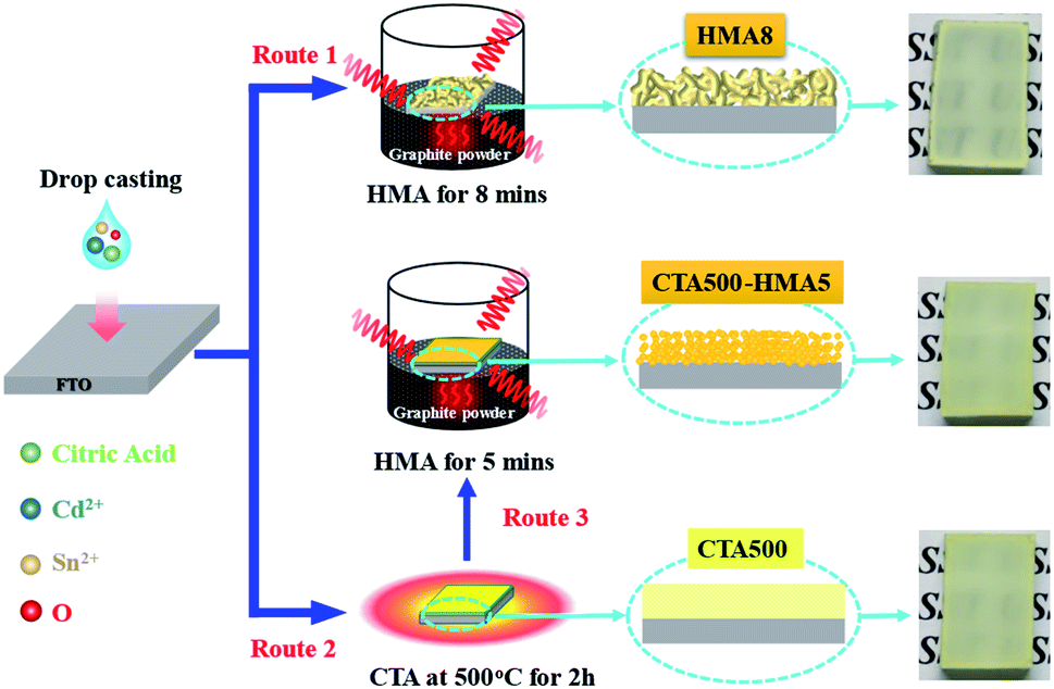 | ||
| Fig. 1 Schematic representation for preparation of Cd2SnO4 thin films. | ||
Scanning electron microscopy (SEM) images show that the as-synthesized samples exhibited a smooth surface (Fig. 2a–c). Compared to CTA500 and CTA500-HMA5, HMA8 consists of nanostructured particles with the highest porosity and roughness. As also evidenced by the cross-sectional SEM observations (insets in Fig. 2a–c), the thickness of CTA500, CTA500-HMA5 and HMA8 was estimated to be 2.52, 2.93 and 2.05 μm, respectively. The section morphology of these samples was altered from compact and very dense for CTA500, surficial sheetlike for CTA500-HMA5 to highly porous and completely fluffy for HTA8. It can reasonably account for the fast crystallization and particle growth rates of Cd2SnO4 under the HMA conditions, thus contributing to shortening charge transfer channels and improve O2-evolving ability. As shown in Fig. 2d–f and S1,† the TEM observations of HMA8 further confirm the formation of the worm-like structured cubic Cd2SnO4 phase with high porosity. The lattice fringes with a spacing of ca. 0.27 nm correspond to the (311) plane of cubic Cd2SnO4 and the corresponding selected area electron diffraction (SAED) pattern (inset) indicates its polycrystalline structure.
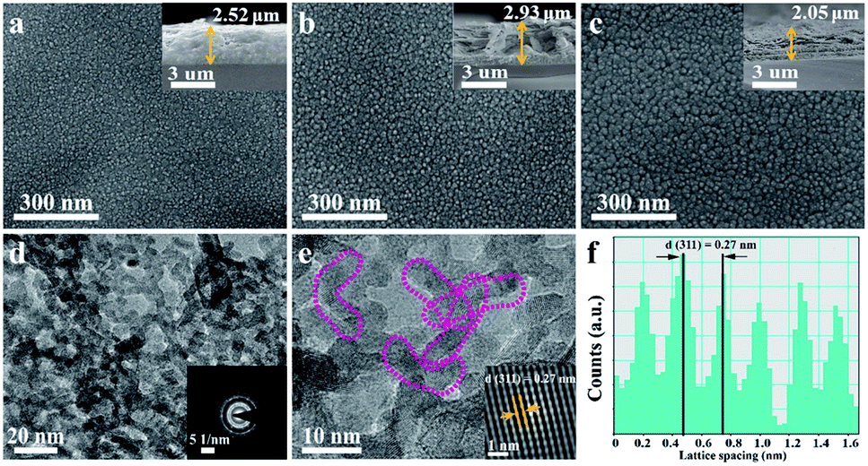 | ||
| Fig. 2 Typical SEM images of (a) CTA500, (b) CTA500-HMA5, and (c) HMA8, the inset corresponds to the cross-sectional view, (d) TEM image and SAED pattern (the inset) of HMA8, (e) HRTEM image of HMA8 and the corresponding auto-correlated HRTEM lattice image (the inset), and (f) the corresponding lattice spacing profile. | ||
The X-ray diffraction patterns of the typical CTA500, CT500-HMA5 and HMA8 samples are presented in Fig. S2 and S3 ESI.† The observed diffraction peaks can be assigned to the formation of the cubic Cd2SnO4 phase with a space group of Fd![[3 with combining macron]](https://www.rsc.org/images/entities/char_0033_0304.gif) m (JPCDS card no. 80-1469), except for those of FTO. The strong peaks located at 32.3° and 33.8° became gradually sharp from CTA500, CT500-HMA5 to HMA8 samples. Meanwhile, their intensity ratios were increased, and the estimated full width half maximum (FWHM) reached the narrowest value of ca. 0.6° in HMA8. The results indicate that the cubic Cd2SnO4 nanocrystals showed a preferred growth orientation due to the HMA process. A detailed discussion of the XRD patterns of the as-synthesized thin films is also given in Fig. S2 and S3.† Generally, the results reveal that the HMA process remarkably promoted the phase crystallinity. In addition, the peak located at 32.3° can be assigned to the (311) plane of the cubic Cd2SnO4 phase, which is supportive of the TEM analysis results. Fig. 3a shows the Raman spectra of the typical CTA500, CT500-HMA5 and HMA samples. The dominant band at ∼639 cm−1 is assigned to the symmetric and asymmetric modes of the Sn–O bonds of cubic Cd2SnO4, in good accordance with the documented literature data, implying that there are no unidentifiable impurities in the samples.8,21,22 The specific surface area and porosity were characterized by using nitrogen adsorption and desorption isotherms, as shown in Fig. 3b. The porous worm-like Cd2SnO4 for HMA8 not only possesses the highest BET surface area of about 21.2 m2 g−1, higher than those of 20.2 m2 g−1 for CT500-HMA5 and 13.7 m2 g−1 for CTA500. The corresponding pore-size distribution further confirms that the HMA process led to the porous feature of the CTA500-HMA and HMA8 samples (inset in Fig. 3b). The porosity gradually increased in the order: CTA500, CTA500-HMA5 and HMA8. The specific worm-like porous structure endows the Cd2SnO4 electrode with a large effective specific surface area, short charge transfer channels and good O2-evolving ability, thus probably accelerating water oxidation reactions.
m (JPCDS card no. 80-1469), except for those of FTO. The strong peaks located at 32.3° and 33.8° became gradually sharp from CTA500, CT500-HMA5 to HMA8 samples. Meanwhile, their intensity ratios were increased, and the estimated full width half maximum (FWHM) reached the narrowest value of ca. 0.6° in HMA8. The results indicate that the cubic Cd2SnO4 nanocrystals showed a preferred growth orientation due to the HMA process. A detailed discussion of the XRD patterns of the as-synthesized thin films is also given in Fig. S2 and S3.† Generally, the results reveal that the HMA process remarkably promoted the phase crystallinity. In addition, the peak located at 32.3° can be assigned to the (311) plane of the cubic Cd2SnO4 phase, which is supportive of the TEM analysis results. Fig. 3a shows the Raman spectra of the typical CTA500, CT500-HMA5 and HMA samples. The dominant band at ∼639 cm−1 is assigned to the symmetric and asymmetric modes of the Sn–O bonds of cubic Cd2SnO4, in good accordance with the documented literature data, implying that there are no unidentifiable impurities in the samples.8,21,22 The specific surface area and porosity were characterized by using nitrogen adsorption and desorption isotherms, as shown in Fig. 3b. The porous worm-like Cd2SnO4 for HMA8 not only possesses the highest BET surface area of about 21.2 m2 g−1, higher than those of 20.2 m2 g−1 for CT500-HMA5 and 13.7 m2 g−1 for CTA500. The corresponding pore-size distribution further confirms that the HMA process led to the porous feature of the CTA500-HMA and HMA8 samples (inset in Fig. 3b). The porosity gradually increased in the order: CTA500, CTA500-HMA5 and HMA8. The specific worm-like porous structure endows the Cd2SnO4 electrode with a large effective specific surface area, short charge transfer channels and good O2-evolving ability, thus probably accelerating water oxidation reactions.
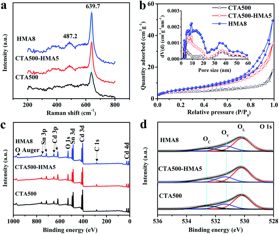 | ||
| Fig. 3 (a) Raman spectra. (b) BET surface area measurement of the Cd2SnO4 photoanodes and pore size distribution (inset) of the Cd2SnO4 photoanodes. (c) Survey scan XPS spectra of CTA500, CTA500-HMA5 and HMA8, respectively. (d) O 1 s XPS spectra of typical CTA500, CTA500-HMA5 and HMA8 samples. | ||
The elemental composition and chemical states of the as-synthesized samples were examined by X-ray photoelectron spectroscopy (XPS). The survey-scan XPS spectra in Fig. 3c show similar surface components of Cd, Sn and O. The region-scan spectra of Cd 3d (Fig. S4a), Sn 3d (S4b†) and O 1s (Fig. 3d) are almost similar, implying that no detectable change in the oxidation states of each element was recorded for these samples. The Cd 3d5/2 and Cd 3d3/2 peaks located at 404.9 and 411.6 eV are in agreement with the literature data for Cd2+.12,23 The binding energies of Sn 3d5/2 and Sn 3d3/2 located at 486.6 and 495.0 eV with an 8.4 eV spin–orbit energy splitting correspond to the oxidation state of Sn4+, which is consistent with the XPS spectrum database of SnO2. Interestingly, the calculated elemental ratios of Cd/Sn derived from the survey-scan XPS spectra were almost equal to about 1.5:1.0 (±0.1) (Table S1†). By using inductively coupled plasma optical emission spectrometry (ICP-OES), the bulk Cd/Sn ratio can be determined to be about 1.4:1.0 (±0.1) (Table S2†), which is a little lower than the surface Cd/Sn ratio. The result suggests that the nominal Cd2SnO4 is a nonstoichiometric composition of Cd2−xSnxO4−y with surface enrichment in Cd. This indicated that the defective Cd2SnO4 is comprised of a great proportion of native structural defects and oxygen vacancies. To gain further understanding on the defect-rich structure, the asymmetric O 1s XPS spectra were deconvoluted into three typical peaks approximately at 530.1, 531.4 and 532.5 eV, which are in line with the literature data.24,25 These peaks are associated with the O2− species in the lattice (OL), oxygen vacancies (OV) and chemisorbed/dissociated (OC) oxygen species. As expected, the atomic ratios of the OV states are indeed high for Cd2SnO4, in order to maintain the charge neutrality of the nonstoichiometric composition (Table S3†). The atomic ratio of the OV states was increased from 22.3 at% for CTA500, 22.9 at% for CTA500-HMA5 to 24.4 at% for HMA8. It is evident that fast hybrid annealing suppressed the surface equilibration and caused more compositional defects, which is believed to facilitate the trapping of photoinduced electrons and holes as will be also discussed later.
The UV-vis absorption spectra of CTA500, CTA500-HMA5 and HMA8 samples in Fig. 4a show a similar steep absorption edge at a wavelength around 485 nm. Accordingly, the band gap (Eg) of cubic Cd2SnO4 can be estimated to be about 2.55 eV by the Tauc plots (inset), which is consistent with the reported values obtained by Ogale, et al.7,14 It is noticeable that for wavelengths above ∼550 nm, the appearance of such a strong and broad absorption feature demonstrated the existence of defect-induced intrinsic trapping states. To give a clear clarification of the energy band alignment for deficient Cd2SnO4, we performed the flat band potential (EFB) measurements using Mott–Schottky (MS) plots and examined the valence band maximum (VBM) by valence-band XPS spectroscopy. As shown in Fig. 4b, the positive MS slopes indicate an n-type semiconducting behavior for deficient Cd2SnO4. It is known from the MS analysis for the n-type semiconductor that the conduction band potential (ECB) is generally 0.1–0.3 V more negative than EFB.26,27 When we used this technique to compare the band potential difference of ECB among these samples, and the EFB was converted to ECB by assuming ECB = EFB − 0.3 V. The ECB can be estimated to be −0.34 V vs. RHE, which is almost identical to the previously reported EFB value of −0.31 V vs. RHE.14 Therefore, the valence band potential (EVB) value can be determined to be about 2.22 V vs. RHE, according to the equation, EVB = Eg + ECB. As shown in Fig. 4c, the valence-band XPS spectra of the CTA500, CTA500-HMA5 and HMA8 samples show a similar VBM of ∼2.15 eV for deficient Cd2SnO4. The energy band values resulting from the valence-band XPS spectra and MS plot analysis are very close, verifying the reasonability of our experimental estimation.28 Moreover, their valence band widths are almost identical, representing similar mobilities of the photogenerated charge carriers.29Fig. 4d illustrates the energy band structure of Cd2SnO4. Due to the trapping of electrons at the near-surface defect states and the accumulation of holes at the surface states, trapping charge carriers in deficient Cd2SnO4 results in a reduction of the charge recombination rate and acceleration of the charge transfer process.30,31,38,39
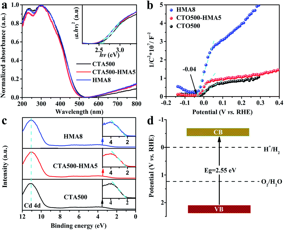 | ||
| Fig. 4 (a) UV-Vis absorption spectra and the Tauc plots (inset) of the CTA500, CTA500-HMA5 and HMA8 samples. (b) Estimation of EFB using MS plots. (c) Estimation of the VBM by valence-band XPS spectroscopy. (d) The proposed energy band structure of deficient Cd2SnO4 determined using Tauc plots, MS plots and valence-band XPS spectroscopy. | ||
PEC performance and stability improvement
To clarify the promotion effect of the HMA treatment, the PEC performance of the as-synthesized samples with different HMA treatment times (X) was evaluated in detail, in corroboration of the above XRD analysis. As shown in Fig. S5a† and 5a, CTA500 exhibited a poor water oxidation activity with a photocurrent of ∼4 μA cm−2 at 1.70 V vs. RHE. By the extra application of the HMA treatment, the PEC performance of CTA-HMAX was significantly increased, reached the maximum photocurrent of ∼13 μA cm−2 at 1.70 V vs. RHE for CTA500-HMA5, and then decreased gradually for CTA500-HMA8 and CTA500-HMA10. Similarly for those samples synthesized by only using the HMA treatment, a dramatic enhancement of solar photocurrent generation was observed in HMA8, showing a steady photocurrent density of ∼25 μA cm−2 at 1.70 V vs. RHE, which is nearly 6-fold and 2-fold higher than that of CTA500 and CTA500-HMA5, respectively (Fig. 5b and S5b†). The results demonstrated that the HMA process plays an important role in PEC performance improvement, which is greatly dependent on the HMA treatment time. For verification of the observed solar photocurrents and better comparison, we further conducted linear sweep voltammetry (LSV) measurements under constant sunlight irradiation. As shown in Fig. 5c, the photocurrent densities of the CTA500, CTA500-HMA5 and HMA8 samples collected from the corresponding LSV curves at 1.7 V vs. RHE are consistent with the chopped ones. To get insight into structure–activity relationships, we further investigated the PEC water oxidation performance of the Cd2SnO4 photoanodes in the presence of 0.1 M Na2SO3 as the hole scavenger. The addition of the Na2SO3 hole scavenger resulted in significantly higher PEC oxidation performance compared to no Na2SO3 hole scavenger. Specifically, the HMA8 photoanode exhibited about 12-times higher photocurrent density of ∼302 μA cm−2 at 1.7 V vs. RHE, corresponding to the higher charge separation efficiency. This indicates that in the absence of an efficient photogenerated hole-extraction mechanism, the charge recombination is quite high, requiring a higher external bias. Major limitations in the achieved photocurrent density from the charge recombination processes were observed at the electrode–electrolyte interface. The stability of the photoanodes was tested at 1.7 V vs. RHE under continuous 1 sun illumination (Fig. 5d). The decay of photocurrent densities for both HMA8 and CTA500-HMA5 is far weaker than that for CTA500. After the stability test, the LSV measurements of these recycled samples show that the performance of CTA500 obviously declined by more than half. No significant decrease was observed in the photocurrent densities of CTA500-HMA5 and HMA8 at 1.70 V vs. RHE (Fig. S7†). This indicated that the utilization of the HMA process can enhance the photogenerated charge separation process, thus delivering continuous and steady photocurrents. We further examined the morphology of these recycled samples by SEM. As shown in Fig. S8,† particle aggregation occurred, especially for CTA500. To characterize the electrical properties of these samples as well as the charge transfer efficiencies, we employed electrochemical impedance spectroscopy (EIS) in the dark and under sunlight irradiation. The EIS Nyquist plots shown in Fig. 5e reveal that the high frequency arc corresponds to the double-layer capacitance (Cdl) in parallel with the charge transfer resistance (Rct) at the contact interface between the electrode/electrolyte solutions. The corresponding arc radii were decreased gradually in the cases of both with and without sunlight irradiation. HMA8 possessed the smallest EIS arc radii, indicating an effective photogenerated charge separation and fast interfacial charge transfer as well as the excellent electrical conductivity to transfer excited electrons from the valence band to the conduction band. In addition, it can be found that the application of the HMA treatment even for several minutes did not affect the electrical conductivity of the FTO substrate, since it provides a relatively high temperature of 700–1000 °C in an extremely short start-up time.16,32 The monochromatic incident photon-to-current conversion efficiencies (IPCE) of CTA500, CTA500-HMA5 and HMA8 photoanodes were also measured as shown in Fig. 5f. The IPCE values for the HMA8 photoanodes are estimated to be about 39% and 18% at 300 nm and 350 nm, respectively which are slightly higher than that of CTA500-HMA5 (37% at 300 nm and 15% at 350 nm) but 1.5 times as high as that of the CTA500 photoanodes. The performance comparison among different typical photoanode materials is provided in Table S5,† showing that the HMA process was beneficial for the enhanced PEC performance. It mainly originated from the promoted charge efficiency via the suppression of charge recombination, since the absorbance (as shown in Fig. S6†) and charge mobility (as shown in Fig. 4c) of these as-synthesized samples are almost identical.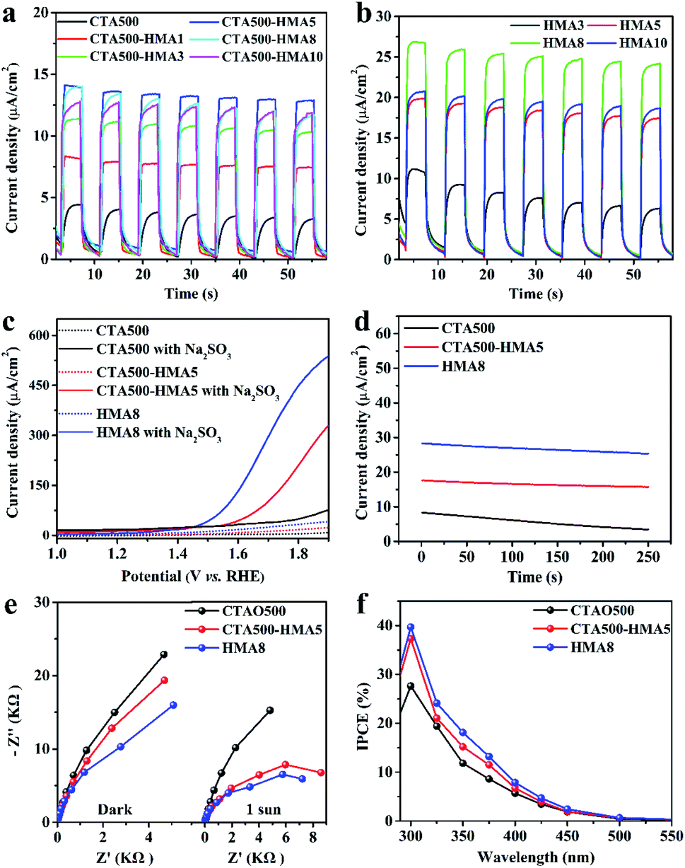 | ||
| Fig. 5 (a) Photocurrent measurements of CTA500 and CTA-HMAX samples under chopped sunlight irradiation in 1 M NaOH solution at 1.7 V vs. RHE. (b) Photocurrent measurements of HMAX samples under chopped sunlight in 1 M NaOH solution at 1.7 V vs. RHE (c) Photocurrent density–potential LSV curves measured in 1 M NaOH solution without and with the addition of 0.1 M Na2SO3 as the hole scavenger (pH 13.6) under simulated sunlight illumination (AM 1.5 G, 100 mW cm−2). (d) Photocurrent decay curves in 1 M NaOH solution at 1.7 V vs. RHE. (e) Nyquist plots at high frequency in the dark and under sunlight illumination. (f) IPCE curves measured in 1 M NaOH/0.1 M Na2SO3 solution at 1.7 V vs. RHE. | ||
Enhanced photogenerated charge separation and transfer dynamics
The enhanced PEC performance could be mainly attributed to the improved bulk charge separation efficiency (ηbulk) and interfacial charge transfer efficiency at the electrode/electrolyte interface (ηsurface). The charge separation efficiency is related to bulk electron–hole recombination, while the interfacial charge transfer efficiency is correlated to the surface electron–hole recombination, and both of them can be quantified by adding a hole scavenger to the electrolyte. Based on the obtained photocurrent curves (Fig. 5c), we further conducted quantitative estimations of ηbulk and ηsurface values, as given in Fig. 6a, b. The as-synthesized photoanodes exhibited similar ηsurface values, but over 13.5-fold and 4.5-fold increases in the ηbulk values of HMA8 and CTA500-HMA5 were observed in comparison with that of CTA500 at a bias of 1.7 V vs. RHE. The quantitative analyses suggest that the fabrication of the Cd2SnO4 photoanodes composed of highly porous worm-like nanoparticles could be an efficient strategy to promote bulk charge separation by shortening the charge diffusion lengths. Fig. 6c–e show photoluminescence (PL) investigations on the fate of photoexcited charge carriers and illustrate schematically the possible charge transfer pathways. The near-band-edge region of the as-synthesized photoanodes was subjected to steady-state PL spectroscopy. Essentially, the weak PL response observed indicated a slow recombination rate and long lifetime of photogenerated charge carriers. HMA8 shows the weakest intensity of PL peaks, compared with those of CTA500 and CTA500-HMA5. These photoanodes exhibited almost the same emission features with the characteristic emission peaks located at about 453, 483 and 563 nm, respectively. The emission band with a peak at ∼483 nm corresponding to ∼2.56 eV can be ascribed to the band-to-band emission of Cd2SnO4. The emission bands occurring apparently at around 453 nm could be the charge transfer of Cd–O and Sn–O in the deficient structure of Cd2SnO4. The obvious band at the highest wavelength of ∼563 nm is related to high-concentration oxygen vacancies, in agreement with our XPS analysis as discussed above and the literature data.33–35 Due to large amounts of photoexcited electrons trapped in the bulk and/or surface oxygen vacancies, they would act as a luminescence quencher and non-radiative center, and probably also lead to the obvious decrease in the PL emission intensity of HMA8.10,36 In addition, other weak bands with peaks spread out in the region from 490 to 540 nm are probably attributed to the presence of structural defects, i.e., deep levels or trap state emissions, which can trap charge carriers prior to their undergoing recombination.2 To further examine the charge carrier dynamics, the powerful nanosecond time-resolved photoluminescence (TRPL) emission decay spectra of the CTA500, CTA500-HMA5 and HMA8 samples were recorded (Fig. 6e). Upon nanosecond photoexcitation, the emission intensities of both samples decayed exponentially on a nanosecond time scale, and the average decay time (τ) was estimated by fitting with exponential components. Localization of charge carriers in these long-lived trap states can facilitate charge separation and potentially enhance photocatalytic activity. The result was consistent with the above steady-state PL results, showing the τavg values of CTA500, CTA500-HMA5 and HMA8 estimated to be about 1.31 ns, 1.37 ns and 1.58 ns, respectively. The extended τavg can be thus attributed to the charge transfer processes facilitated by the HMA treatment, responsible for the reduced charge recombination and shortened hole diffusion length.37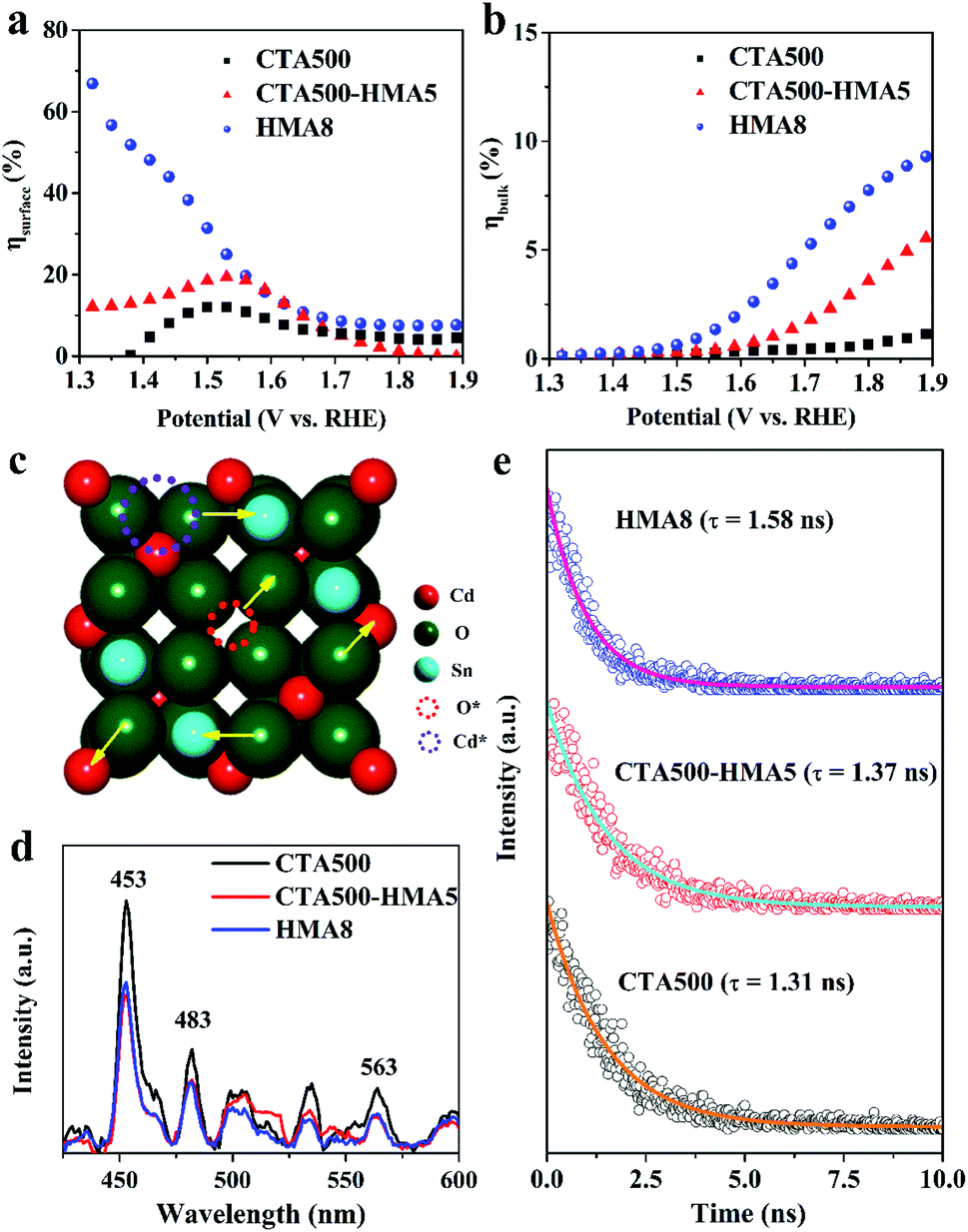 | ||
| Fig. 6 Interfacial charge transfer efficiency (ηsurface) (a) and bulk charge separation efficiency (ηbulk) (b) at the electrode/electrolyte interfaces for CTA500, CTA500-HMA5 and HMA8 under AM 1.5 G illumination (100 mW cm−2). (c) Schematic of the deficient Cd2SnO4 structure within possible charge transfer pathways. (d) The steady-state PL spectra and (e) the nanosecond time-resolved PL spectra of CTA500, CTA500-HMA5 and HMA8 photoanodes. | ||
During PEC solar water oxidation reactions with the application of an external anodic bias, the photoexcited electrons and holes would move oppositely to the back contact and the surface of the electrode, travelling through the solid nanoparticles, and reaching the electrode/electrolyte interfaces before recombination. By integrating the above analysis results, differential photo-electrocatalytic mechanisms have been proposed for CTA500, CTA500-HMA5 and HMA8 photoanodes (Fig. 7). Specifically, the possible reasons behind the superior PEC performance of the HMA8 photoanodes were also provided. The HMA8 photoanode comprised of worm-like and highly porous nanocrystals exhibited a large specific surface area, high degree of phase crystallization and high-concentration defects. In contrast, the CTA500 photoanode exhibited a small specific surface area, low degree of phase crystallization and long charge diffusion length. Even with the extra HMA treatment, the CTA500-HMA5 photoanode with a surficial sheetlike feature consisted of a large quantity of interparticle boundaries. Besides these, various physicochemical characterization studies, electrochemical analysis and hole scavenger photooxidation experiments reveal that the bulk charge separation efficiency contributed greatly to the enhanced PEC performance in HMA8, achieving a long charge carrier lifetime, short charge diffusion distance and low recombination rate. Therefore, more holes would be able to escape from recombination centers before reaching the electrode surface in HMA8 than in CTA500 and CTA500-HMA5. In addition, the special morphology of Cd2SnO4 in HMA8 may also contribute to good O2-releasing ability, thus accelerating the solar water oxidation reaction.
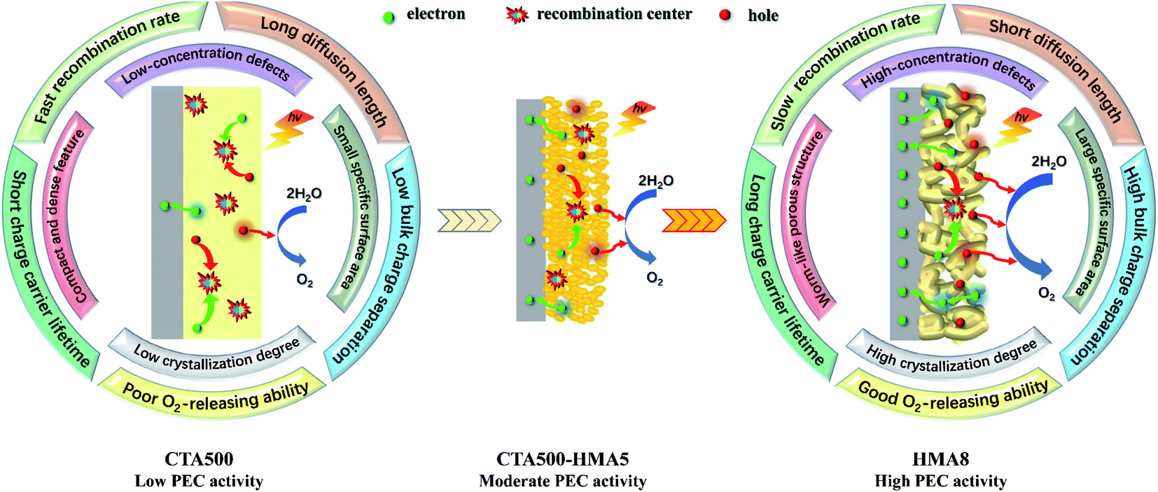 | ||
| Fig. 7 Proposed photoelectrocatalytic mechanisms for CTA500, CTA500-HMA5 and HMA8 photoanodes. | ||
Conclusions
In summary, we successfully synthesized more efficient Cd2SnO4 photoanodes by the HMA method for the first time. Direct HMA for only 8 min resulted in formation of worm-like and highly porous cubic Cd2SnO4, achieving a large specific surface area and high degree of phase crystallization as well as high-concentration defects. A remarkable enhancement of solar photocurrent in HMA8 was observed, which is 6-fold and 2-fold higher than the CTA treated one and the combined CTA-HMA treated one, respectively. It stems from the improved charge carrier trapping, recombination and transfer processes related to high bulk charge separation efficiency, short charge diffusion length, long charge carrier lifetime, and good O2-releasing ability. Considering less energy-loss and time-consumption, the HMA process is an ideal method to construct photocatalytic materials for potential applications. We also note that a high external bias is needed, but Cd2SnO4 is suitable for further application in doping engineering and non-noble metal-cocatalyst deposition.Conflicts of interest
There are no conflicts to declare.Acknowledgements
We greatly appreciate the financial support from the National Natural Science Foundation of China (51572173), Shanghai Municipal Science and Technology Commission of Academic/Technology Research Leader Program (19XD1422900), Carbon Peak&Carbon Neutral Project (21DZ1207900), and the Hundred Talents Program of the Chinese Academy of Sciences (E11YB515).References
- K. Jeyadheepan, M. Thamilselvan, K. Kim, J. Yi and C. Sanjeeviraja, J. Alloys Compd., 2015, 620, 185–191 CrossRef CAS.
- P. Sakthivel, R. Murugan, S. Asaithambi, M. Karuppaiah, G. Vijayaprasath, S. Rajendran, Y. Hayakawa and G. Ravi, Ceram. Int., 2018, 44, 2529–2538 CrossRef CAS.
- R. Kumaravel, V. Krishnakumar, V. Gokulakrishnan, K. Ramamurthi and K. Jeganathan, Thin Solid Films, 2010, 518, 2271–2274 CrossRef CAS.
- A. Gulino and I. Fragalà, J. Mater. Chem., 1999, 9, 2837–2841 RSC.
- X. Li, T. A. Gessert and T. Coutts, Appl. Surf. Sci., 2004, 223, 138–143 CrossRef CAS.
- B. Radhouane, B. Noureddine and A. B. Mohamed, Eur. Phys. J.: Appl. Phys., 2015, 69, 30302 CrossRef.
- A. Deshpande, S. Kelkar, S. Rayalu and S. Ogale, J. Mater. Chem. A, 2014, 2, 492–499 RSC.
- G. Zhang, Z. Fu, Y. Wang, H. Wang and Z. Xie, RSC Adv., 2015, 5, 83922–83930 RSC.
- S. Dinesh, M. Anandan, V. Premkumar, S. Barathan, G. Sivakumar and N. Anandhan, Mater. Sci. Eng., B, 2016, 214, 37–45 CrossRef CAS.
- G. Preethi, R. Balan, S. Koppala and H. P. Nagaswarupa, Mater. Res. Express, 2019, 6, 105537 CrossRef CAS.
- A. W. Metz, M. A. Lane, C. R. Kannewurt, K. R. Poeppelmeier and T. J. Marks, Chem. Vap. Deposition, 2004, 10, 297–300 CrossRef CAS.
- A. Abrutisa, G. Valincius, G. Baltrunas, L. Parafionovic, A. Valiuniene and Z. Saltytea, Thin Solid Films, 2007, 515, 6817–6823 CrossRef.
- D. O. Rivera, G. T. Delgado, J. M. Marín, R. C. Pérez, M. A. A. Frutis and O. Z. Ángel, J. Mater. Sci.: Mater. Electron., 2018, 29, 20470–20475 CrossRef.
- S. A. Kelkar, P. A. Shaikh, P. Pachfule and S. B. Ogale, Energy Environ. Sci., 2012, 5, 5681–5685 RSC.
- J. H. Kim, J. W. Jang, J. Y. Kim, S. H. Choi, G. Magesh and J. S. Lee, Adv. Energy Mater., 2015, 5, 1401933 CrossRef.
- H. Zhang and J. S. Lee, Acc. Chem. Res., 2019, 52, 3132–3142 CrossRef CAS PubMed.
- Y. J. Jang, Y. B. Park, H. E. Kim, Y. H. Choi, S. H. Choi and J. S. Lee, Chem. Mater., 2016, 28, 6054–6061 CrossRef CAS.
- H. Zhang, J. H. Park, W. J. Byun, M. H. Song and J. S. Lee, Chem. Sci., 2019, 10, 10436–10444 RSC.
- Q. Cao, S. Yang, Q. Gao, L. Lei, Y. Yu, J. Shao and Y. Liu, ACS Appl. Mater. Interfaces, 2016, 8, 7854–7861 CrossRef CAS PubMed.
- G. T. Ivan, Y. G. Geertzema, A. S. M. Ismail, T. L. Lee, D. Groot, M. F. Frank and B. M. Weckhuysen, ChemPhotoChem, 2019, 3, 1238–1240 CrossRef.
- S. Kumar and A. Ojhaa, AIP Adv., 2013, 3, 052109 CrossRef.
- J. Q. Hu, X. L. Ma, N. G. Shang, Z. Y. Xie, N. B. Wong, C. S. Lee and S. T. Lee, J. Phys. Chem. B, 2002, 106, 3823–3826 CrossRef CAS.
- D. A. Cristaldi, G. Impellizzeri, F. Priolo, T. Gupta and A. Gulino, J. Phys. Chem. C, 2012, 116, 3363–3368 CrossRef CAS.
- X. Zhang, J. Qin, Y. Xue, P. Yu, B. Zhang, L. Wang and R. Liu, Sci. Rep., 2014, 4, 4596 CrossRef PubMed.
- S. Wang, P. Chen, Y. Bai, J. H. Yun, G. Liu and L. Wang, Adv. Mater., 2018, 30, 1800486 CrossRef PubMed.
- W. J. Chun, A. Ishikawa, H. Fujisawa, T. Takata, J. N. Kondo, M. Hara, M. Kawai, Y. Matsumoto and K. Domen, J. Phys. Chem. B, 2003, 107, 1798–1803 CrossRef CAS.
- H. You, Z. Wu, L. Zhang, Y. Ying and H. Huang, Angew. Chem., Int. Ed., 2019, 58, 11779–11784 CrossRef CAS PubMed.
- A. Hankin, F. E. B. Lora, J. C. Alexander, A. Regoutz and G. H. Kelsall, J. Mater. Chem. A, 2019, 7, 26162–26176 RSC.
- V. Etacheri, G. Michlits, M. K. Seery, S. J. Hinder and S. C. Pillai, ACS Appl. Mater. Interfaces, 2013, 5, 1663–1672 CrossRef CAS PubMed.
- R. Chen, S. Pang, H. An, T. Dittrich, F. Fan and C. Li, Nano Lett., 2018, 19, 426–432 CrossRef PubMed.
- V. Ghodsi, S. Jin, J. C. Byers, Y. Pan and P. V. Radovanovic, J. Phys. Chem. C, 2017, 121, 9433–9441 CrossRef CAS.
- J. Y. Kim, D. H. Youn, J. H. Kim, H. G. Kim and J. S. Lee, ACS Appl. Mater. Interfaces, 2015, 7, 14123–14129 CrossRef CAS PubMed.
- S. Zhang, Z. Liu, D. Chen, Z. Guo and M. Ruan, Chem. Eng. J., 2020, 395, 125101 CrossRef CAS.
- J. A. R. Ramón, D. L. Sánchez, M. H. Zaldívar and U. Pal, Mater. Sci. Semicond. Process., 2015, 40, 943–953 CrossRef.
- A. Jiamprasertboon, A. Waehayee, N. Chanlek, N. Yong, S. Suthirakun and T. Siritanon, J. Alloys Compd., 2019, 783, 28–36 CrossRef CAS.
- A. Kumar, S. Babu, A. S. Karakoti, A. Schulte and S. Seal, Langmuir, 2009, 25, 10998–11007 CrossRef CAS PubMed.
- R. Shen, L. Zhang, X. Chen, M. Jaroniec, N. Li and X. Li, Appl. Catal., B, 2020, 266, 118619 CrossRef CAS.
- J. Bai, R. Shen, W. Chen, J. Xie, P. Zhang, Z. Jiang and X. Li, Chem. Eng. J., 2022, 429, 132587 CrossRef CAS.
- X. Liu, S. Gu, Y. Zhao, G. Zhou and W. Li, J. Mater. Sci. Technol., 2020, 56, 45–68 CrossRef CAS.
Footnotes |
| † Electronic supplementary information (ESI) available. See DOI: 10.1039/d1na00828e |
| ‡ These authors contributed equally to the work. |
| This journal is © The Royal Society of Chemistry 2022 |