
 Open Access Article
 This Open Access Article is licensed under a Creative Commons Attribution-Non Commercial 3.0 Unported Licence
Solvent composition regulates the Se![[thin space (1/6-em)]](https://www.rsc.org/images/entities/h2_char_2009.gif) :Sb ratio in antimony selenide nanowires deposited from thiol–amine solvent mixtures†
:Sb ratio in antimony selenide nanowires deposited from thiol–amine solvent mixtures†
A.
Vashishtha
a,
O.
Vana
a and
E.
Edri
 *abc
*abc
aDepartment of Chemical Engineering, Ben-Gurion University of the Negev, Be'er-Sheva 8410501, Israel. E-mail: edrier@bgu.ac.il
bIlse Katz Institute for Nanoscale Science and Technology, Be'er-Sheva 8410501, Israel
cBlechner Center for Industrial Catalysis and Process Development, Be'er-Sheva 8410501, Israel
First published on 20th December 2021
Abstract
Antimony selenide (Sb2Se3), a V2VI3 semiconductor with an intriguing crystal structure, has demonstrated improved power conversion and solar-to-hydrogen efficiencies in recent years. Depositing antimony selenide nanowires (NWs) from a solution such as a thiol![[thin space (1/6-em)]](https://www.rsc.org/images/entities/char_2009.gif) :amine “alkahest” ink is a low-cost and facile route to deposit high surface area photocathodes. However, little is known about the correlations between the solvent composition and the crystallites' structure and optoelectronic properties, which are crucial for photovoltaic and photoelectrochemical applications. We found that the Se:Sb ratio in the NWs decreases from 3:2 to less than 1:1 with decreasing thiol:amine ratio in the ink used for deposition but not in the solvent mixture used for dissolving the metals. The reduced Se:Sb ratio in the solid NWS correlates with an optical bandgap wider by ∼0.3 eV in comparison to stoichiometric NWs, a decrease of the NWs diameter from 180 to 30 nanometers, and a ∼0.2 eV larger work function. In addition, we found that the Se:Sb ratio is not uniform along the NWs, which causes a surface potential increase near the tips of the NWs due to a lower Se:Sb ratio near the NWs tips. The increased surface potential near the tips corresponds to a driving force, due to doping or graded bandgap broadening, that facilitates the migration of photoexcited electrons towards the NW tips. Our findings unlock a path for fine-tuning the optoelectronic properties of antimony selenide towards improving the performance of antimony selenide solar cells and photocathodes.
:amine “alkahest” ink is a low-cost and facile route to deposit high surface area photocathodes. However, little is known about the correlations between the solvent composition and the crystallites' structure and optoelectronic properties, which are crucial for photovoltaic and photoelectrochemical applications. We found that the Se:Sb ratio in the NWs decreases from 3:2 to less than 1:1 with decreasing thiol:amine ratio in the ink used for deposition but not in the solvent mixture used for dissolving the metals. The reduced Se:Sb ratio in the solid NWS correlates with an optical bandgap wider by ∼0.3 eV in comparison to stoichiometric NWs, a decrease of the NWs diameter from 180 to 30 nanometers, and a ∼0.2 eV larger work function. In addition, we found that the Se:Sb ratio is not uniform along the NWs, which causes a surface potential increase near the tips of the NWs due to a lower Se:Sb ratio near the NWs tips. The increased surface potential near the tips corresponds to a driving force, due to doping or graded bandgap broadening, that facilitates the migration of photoexcited electrons towards the NW tips. Our findings unlock a path for fine-tuning the optoelectronic properties of antimony selenide towards improving the performance of antimony selenide solar cells and photocathodes.
Introduction
Antimony selenide is an earth-abundant, low-cost, and low-toxicity material with an appropriate bandgap for photovoltaic (PV) and photoelectrocatalytic (PEC) applications. Its low electron affinity, large absorption coefficient (>105 cm−1 at λ ∼ 600 nm), decent carrier mobility (∼10 cm2 V−1 s−1), and long lifetime (∼60 ns) add to the attractiveness of antimony selenide for these applications.1,2 Moreover, crystalline antimony selenide has an orthorhombic structure (stibnite; Fig. 1) consisting of (Sb4Se6)n ribbons covalently linked along the chain-axis direction ([hk1]) and held together by van der Waals bonds in the perpendicular directions (e.g., [1kl]). Ideally, a defect-free ribbon has a closed-shell electronic structure, and hence grains with surfaces perpendicular to the c axis are supposedly defect-free—an exquisite quality for thin-film PV devices and photocathodes.3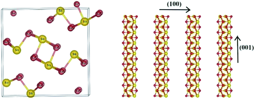 | ||
| Fig. 1 Crystal structure of antimony selenide: Sb2Se3 (orthorhombic) composed of (Sb4Se6)n ribbons stacked in parallel in the (001) direction. | ||
In 2015, Tang and coworkers reported a breakthrough power conversion efficiency (PCE) for Sb2Se3 thin-film solar cells.3 Several reports on the properties and applications of antimony selenide, including further improvements in PCE, were published in the following years.4–8 Thin films of antimony selenide have also been successfully used as photocathodes for the hydrogen evolution reaction.9–11 These achievements motivate further exploration of low-cost and straightforward deposition methods of this material, such as deposition methods based on the thiol:amine “alkahest” solution inks. Yet, to facilitate further progress and utility of these inks for these applications, the connection between the processing method of the materials and their properties with relation to the proposed applications needs to be established.
Solution-based processes constitute a potentially low-cost and simple way to prepare functional materials. Several methods to deposit antimony selenide from a solution are available such as chemical bath deposition and electrodeposition.12–14 However, these methods often result in nanocrystalline films that lack the preferred orientation needed to exploit the unique properties of antimony selenide. Solution casting of dissolved elemental precursors prepared through a “dimensional reduction” approach constitutes a facile method that results in larger microcrystals, more suitable for PEC and PV.15
Hydrazine is an effective solvent for metal chalcogenide processing,15 but its hazardous, toxic, and carcinogenic nature limits its industrial use and scalability.16,17 A promising alternative methodology gaining interest in recent years uses a reducing/coordinating solvent mixture consisting of a primary amine and an alkyl thiol to dissolve a wide range of metals and chalcogens (elemental or ionic forms).18 The formed “ink” is later used to deposit metal chalcogenides by, e.g., spin coating, followed by a low-temperature thermal processing step. The dissolving power of thiol:amine mixtures towards elemental main group metals and chalcogens (Se readily dissolves in such mixtures up to a concentration of 38 wt%) was demonstrated by several groups.19–21 Furthermore, Brutchey, Agrawal, and coworkers expanded the palette of dissolved metals22–24 and the uses of this methodology by preparing high-quality thin films for photovoltaic25,26 and electrocatalytic applications,27 and developed new colloid synthesis routes.28 There are two main mechanisms for describing the dissolution of a chalcogenide in the thiol:amine solvents or metals. The two mechanisms imply that adding an excess of amine or thiol:amine relative to the chalcogen content facilitates the formation of smaller chains of the chalcogenide. Other dissolution mechanisms of main block and transition metals describe the formation of a metal thiolate complex without the chalcogen being part of the molecular species' structure. The antimony case appears to be slightly exceptional because it does not dissolve without adding a chalcogen, which suggests that the molecular species include both the chalcogen and antimony ions. Still, little is known about the solution composition, crystallization process, how they are affected by the precursors' molecular structure, and how they affect the structural and optoelectronic properties of the solid.
Here, we show that the Se:Sb stoichiometry in antimony selenide NWs can be tuned by modifying the solvents ratio in a precursor mixture consisting of Sb and Se dissolved in ethylenediamine (en) and 1,2-ethanedithiol (EDT). This, in turn, affects the optical bandgap of the solid, the NWs' average diameter, and work function. This finding will assist in developing antimony selenide nanomaterials towards their incorporation into PV and PEC devices.
Experimental
Chemicals and reagents
Antimony powder (100 mesh, 99.5%; Sigma-Aldrich, St. Louis, Missouri), selenium powder (100 mesh, 99.99%; Alfa Aesar, Heysham, UK), sulfur powder, 1,2-ethanedithiol (EDT, >98%; Alfa Aesar), ethylenediamine (en, >99%; Acros Organics, Geel, Belgium). All the reagents were used without additional purification.Glass substrates were cleaned by immersion in freshly prepared Piranha solution (4:1 vol 98% H2SO4:30% H2O2; CAUTION: exothermic reaction) and then dried under an N2 stream. Fluorine-doped tin oxide (FTO) glass substrates (FTO glass TEC 15A, 2.2 mm thick; XOPFisica) were cut, cleaned by sequential sonication in acetone, isopropanol, Alconox solution, and deionized (DI) water for 30 minutes each, dried under an N2 stream, and treated in a UV-ozone cleaner (Ossila Ozone Cleaner) for 20 minutes. An Au-coated Si wafer was prepared by depositing 10 nm of Ti followed by 100 nm of Au with a VST e-beam evaporator.
Dilution series
We examined a total of four dilution series: pre/post-dissolution series, which refer to dilutions made before or after the dissolution and filtration step, respectively, and en or en:EDT dilution series, which refer to dilutions with en or en:EDT, respectively.
:EDT dilution series, and en dilution series.
:1 solution was prepared by using equal volumes of the stock solution and en. Similarly, we prepared solutions with a 1:4, 1:5, 1:10, and 1:20 ratio of stock solution to en.
![[thin space (1/6-em)]](https://www.rsc.org/images/entities/b_char_2009.gif) :EDT dilution series.
We diluted the stock solution with different volumes of en–EDT mixtures while keeping the en:EDT ratios in the diluted solutions unchanged. We prepared 1:n (v/v) diluted solutions using the en–EDT solvent mixture for dilution where n = 1, 4, 5 and 10.
:EDT dilution series.
For this series, we prepared four solutions by dissolving 3.21, 1.60, 0.80, and 0.40 mmol of Sb with 4.81, 2.40, 1.20, and 0.60 mmol of Se, respectively, in 1.6 mL of en and 0.4 mL of EDT. Here, the molar ratio of the metals and solvents was maintained, but the total solids concentration was varied. These solutions were labeled as AP-4.8–3.2 (AP for “as prepared,” followed by the respective number of millimoles), AP-2.4–1.6, AP-1.2–0.8, and AP-0.6–0.4, respectively. The solutions were then heated and filtered, similarly to the stock solution.
:thiol ratio constant. In this experiment, we used 1.6, 2.0, 2.4, 2.8, 3.2, and 3.6 mL of en and 0.4 mL of thiol, and these solutions were labelled as AP-4:1 (AP-en:EDT), AP-5:1, AP-6:1, AP-7:1, AP-8:1, and AP-9:1, respectively. The solutions were then heated and filtered, similarly to the stock solution.
:1, 1:5, and 1:10 stable solutions.
:EDT dilution series.
We diluted the stock solution with different volumes of en–EDT mixtures while keeping the en:EDT ratios in the diluted solutions unchanged. We prepared 1:n (v/v) diluted solutions using the en–EDT solvent mixture for dilution where n = 1, 4, 5 and 10.
:EDT dilution series.
For this series, we prepared four solutions by dissolving 3.21, 1.60, 0.80, and 0.40 mmol of Sb with 4.81, 2.40, 1.20, and 0.60 mmol of Se, respectively, in 1.6 mL of en and 0.4 mL of EDT. Here, the molar ratio of the metals and solvents was maintained, but the total solids concentration was varied. These solutions were labeled as AP-4.8–3.2 (AP for “as prepared,” followed by the respective number of millimoles), AP-2.4–1.6, AP-1.2–0.8, and AP-0.6–0.4, respectively. The solutions were then heated and filtered, similarly to the stock solution.
:thiol ratio constant. In this experiment, we used 1.6, 2.0, 2.4, 2.8, 3.2, and 3.6 mL of en and 0.4 mL of thiol, and these solutions were labelled as AP-4:1 (AP-en:EDT), AP-5:1, AP-6:1, AP-7:1, AP-8:1, and AP-9:1, respectively. The solutions were then heated and filtered, similarly to the stock solution.
:1, 1:5, and 1:10 stable solutions.
Deposition of NWs
Aliquots of the solutions (200 μL) were spin-coated on the substrate (2 × 1.5 cm) at 1500 rpm for 60 s, then annealed at 150 °C for 10 min to remove the solvents and then at 300 °C for 5 min to form the NWs; the thermal treatment was carried out under N2 purging at ca. 50 sccm, and a ramp rate of 3.33 °C min−1 was used to reach each annealing temperature. The yellow spin-coated solution turned to a lustrous grey solid after annealing.Physical characterization
The transmittance and diffuse reflectance of the samples were measured using a UV-Vis-NIR Cary 5000 spectrophotometer equipped with an integrating sphere.A Verios XHR 460L scanning electron microscope (SEM) equipped with an energy dispersive spectroscopy (EDS) apparatus was used for high-resolution imaging and elemental analysis at 3 keV and 15 keV, respectively. SEM samples were prepared by cutting 1 cm × 1 cm square of NWs deposited substrates; SEM images were taken in secondary electron (SE) mode using a through-the-lens (TLD) detector.
X-ray diffraction (XRD) was carried out in a PANalytical's Empyrean multi-purpose diffractometer under Cu Kα1 (λ = 1.54 Å) radiation produced at 40 kV and 30 mA, using a 3° min−1 scan rate. XRD data were used to calculate the strain in the Sb2Se3 NWs. The interplanar spacing (d value) was calculated from Bragg's diffraction equation, and the percentage of strain (ε) was calculated by the formula given below.
Raman spectra were collected using a LabRam HR Evolution instrument from Horiba at a resolution of 1.3 cm−1 using a 633 nm laser excitation wavelength. We noted the presence of a peak around 252 cm−1 for the antimony selenide NWs deposited from AP solutions. This peak is related to Sb2O3, which spontaneously formed on the antimony selenide film surface due to the material's oxidation caused by laser heating during the Raman measurement.29 In our case, photo-oxidation of Sb2Se3 happened when a laser power >0.39 mW was used; to minimize this artifact, we recorded the Raman spectra of NWs deposited from diluted solutions using ≤0.39 mW laser power. The measurements were recorded from 60 to 1000 cm−1 under ambient conditions with a 5 s collection time.
X-ray photoelectron spectroscopy (XPS) was performed using an Al Kα excitation source in a Thermo Scientific ESCALAB 250. TEM imaging and EDS analyses were carried out in a JEOL JEM 2100F; a 200 keV accelerating voltage was used for high-resolution images and elemental analyses. TEM samples were prepared by dispersing the Sb2Se3 NWs in methanol and dropping the resulting dispersion on a carbon-coated copper grid. The high-resolution TEM images were recorded in bright-field mode.
Surface potential measurements
Surface photovoltage (SPV) and contact potential difference (CPD) were performed in a commercial KP technology Ltd. system in a non-contact Kelvin probe configuration. Electrical contact to the sample was made to the FTO or Au. Light-emitting diodes (LED) of 700 nm and 1200 nm were used as the photon source, and samples prepared on FTO-coated glass were used. The surface potential of antimony selenide samples was measured from the top and back sides by Kelvin probe force microscopy (KPFM). Samples for topside imaging were spin-coated on FTO glass. The antimony selenide was electrically grounded using silver paste and a short wire, and the exposed antimony selenide surface was analyzed using a Cypher-ES Asylum Research microscope (Oxford Instruments). The topography was recorded in AC imaging mode by scanning the sample surface with a scan rate of 0.5 Hz. A conductive probe coated with Ti– Pt (NSC14\Ti–Pt) with a force constant of 5 N m−1 and resonant frequency of 160 kHz was used for the measurements. For mapping the surface potential, nap mode was used, and nap parameters, such as drive amplitude, tip-sample bias, nap gain, and delta height, were adjusted. Delta height was varied from 0 to some negative values. After adjusting the nap parameters, surface potential images were recorded. Note that because of the different wiring in the KPFM and CPD systems, a more positive CPD value indicates a larger work function of the sample, whereas a more positive surface potential in the KPFM indicates a smaller work function.Results
In the post-dissolution en-dilution series, we deposited antimony selenide NWs on FTO glass from a solution diluted with en after the dissolution of the metals by spin-coating and heating on a hot plate under a continuous flow of N2 (see the Experimental section for details). The normalized diffuse reflectance spectra (DRS) show that the onset of absorption shifts towards higher energy, indicating a broadening of the optical bandgap of the NWs, as the en:EDT ratio in the solution increases. In addition, the average diameter and length of the nanowires decreases as the en:EDT ratio increases, as is evident in the SEM images (Fig. 2B).
 | ||
| Fig. 2 Increase in the bandgap of antimony selenide with decreasing nanowires' diameter—the correspondence between color and solution is indicated on the images in (B). (A) Diffused reflectance spectroscopy of antimony selenide NWs deposited from en:EDT solvent mixtures. (B) Scanning electron microscopy (SEM) images of antimony selenide NWs deposited from en–EDT solvent mixtures with increasing en:EDT ratio. The diameter of the NWs decreases as the en:EDT ratio increases. The average diameter of the NWs was calculated from the SEM micrographs by the sampling of 74 NWs for each solution composition (see the histograms in ESI Fig. S1†). We inferred the optical bandgap of the NWs from the onset of the linear region in each of the reflectance spectra.30 | ||
In addition to the bandgap widening and the smaller diameter, we found that the Se:Sb ratio decreases from 1.46 for NWs prepared from AP solution (a ratio of 1.5 is expected for Sb2Se3) to 0.72 for NWs prepared from a solution diluted ten times by volume with en (1:10). The ratio values obtained from SEM-EDS (which, in this case, probes the whole volume of the sample) and XPS (which only probes the surface) closely match, except for the 1:10 sample, where XPS analysis indicates a higher Se:Sb ratio than EDS (possibly due to the significantly different morphology of sample 1:10 relative to lower dilutions; Table 1). A similar correlation between the en:EDT ratio in the solution and the Se:Sb ratio in the final material was found via TEM-EDS (see below). To quantify the oxygen content and eliminate effects possibly stemming from solvent–substrate interaction, we also analyzed the composition of NWs deposited on an Au-coated Si wafer to provide an oxygen-free background (see ESI Table S5†). We found that the atomic percentages of oxygen and sulfur (probably from EDT decomposition) were invariable with the en:EDT ratio, but the percentage of sulfur was higher for the samples deposited on Au than for those deposited on glass (6 at% at most for samples deposited on Au, and 2.9 at% for samples deposited on glass). Nonetheless, the sulfur and oxygen contents are insufficient to make up for the Se deficiency (or Sb excess), and regardless of the substrate we used, a higher en:EDT ratio in the precursor solution results in a lower Se:Sb ratio in the final material. These results suggest that NWs deposited from a solution with a high en:EDT ratio in the post-reaction en-dilution series has a significant Se deficiency or Sb excess.
:Sb ratio deposited from en:EDT mixtures with various molar ratios
| Sample name | en:EDT molar ratio |
Se:Sb ratio by SEM-EDS |
Se:Sb ratio by XPS |
Average diameter (nm) |
|---|---|---|---|---|
| AP | 4.97 | 1.46 ± 0.03 | 1.52 ± 0.12 | 187 ± 54 |
| 1:1 |
5.13 | 1.31 ± 0.05 | 1.34 ± 0.04 | 108 ± 47 |
| 1:4 |
5.59 | 1.25 ± 0.04 | 68 ± 24 | |
| 1:5 |
5.76 | 1.25 ± 0.01 | 1.24 ± 0.09 | 54 ± 27 |
| 1:10 |
6.54 | 0.72 ± 0.07 | 0.98 ± 0.01 | 32 ± 10 |
In comparison to the post-dissolution en dilution series, we tested the effect of dilution with en:EDT before and after the solution was formed and the effect of increasing with en:EDT in the metal dissolution step (see the experimental section for more details). In the post-dissolution en:EDT dilution series, we noticed that NWs deposited from diluted solutions showed a more minor blue shift in the bandgap (at most ∼0.1 eV in the NWs deposited from the highest diluted solutions; Fig. S2†) in comparison to NWs deposited in the post-dissolution en dilution series (Fig. 2). In addition, we found that NWs deposited from a more diluted ink had a smaller diameter and Se:Sb ratio (Fig. S3 and Table S1†), although not as small as the Se:Sb ratio in post-dissolution en dilution series (vide infra). In the pre-dissolution en:EDT dilution series, the NWs absorbance blue-shifted by <0.1 eV as the metal–chalcogen concentration decreased, whereas the diameter and length of the NWs were invariable with respect to metal–chalcogen concentration (ESI Fig. S4 and S5†). In the pre-dissolution en dilution series, we observed a blue shift of ∼0.1 eV in the most diluted ink but no variations of the bandgap at lower dilutions (ESI Fig. S6†). The diameter and length of the NWs in this series were not affected by dilution either (ESI Fig. S7†). Finally, we compared the bandgap variation in antimony sulfide NWs deposited from solutions at various en:EDT ratios (analogous to the post-reaction en-dilution series above). We found that the absorption onset shifted by ∼0.1 eV, and a decrease in diameter was evident for those NWs prepared from solutions containing high en:EDT ratios (ESI Fig. S8†). A similar correlation between the en:EDT and chalcogen:metal ratios were found in the antimony sulfide NWs, where the S:Sb ratio changed from ∼1.35 (AP) to ∼0.86 (10:1 en:EDT). Therefore, the chalcogen:metal ratios in the NWs, and the NWs structure are affected by the en:EDT ratio in both antimony selenide and sulfide, but the optical band gap shift is much more pronounced in the antimony selenide case. These observations, summarized in Table 2, indicate that diluting the solution after the metals were dissolved with en had the most significant impact on the solids' bandgap, average diameter and length, and Se:Sb ratio.
:Sb ratio in the solid
| Dilution series name | Maximal bandgap widening | % max. change in Se:Sb ratioa,b |
% max. change in NWs diameter |
|---|---|---|---|
| a % max change = (max value − min value)/(max value). b From SEM-EDS; see also Table 2 and ESI. | |||
| Sb–Se post-dissolution en | ∼0.3 eV | 50% | ∼83% |
| Sb–Se post-dissolution en:EDT |
∼0.1 eV | 16% | ∼44% |
| Sb–Se pre-dissolution en | <0.1 eV | 13% | ∼40% |
| Sb–Se pre-dissolution en:EDT |
<0.1 eV | 9% | ∼20% |
| Sb–S post-dissolution en | ∼0.1 eV | 36% | |
The significant variations in the Se:Sb ratio affect the local structure in the solid, as reflected in X-ray diffraction and Raman scattering. The XRD (Fig. 3) pattern of all the NWs samples deposited from various en:EDT ratios is compatible with the diffraction pattern of antimony selenide (ICSD card no. 194837), indicating that no additional crystalline phase had formed at a concentration that can be detected by XRD (see also ESI Fig. S11†). Nonetheless, several XRD peaks are shifted to higher reflection angles as the en:EDT ratio of the solution precursor to the NWs increases (e.g., peak at 32.24° associated with the (221) plane and at 32.30° associated with (301); see Fig. 3B). We attribute these shifts to strain in the NWs lattice.31,32 The calculated strain percentages from XRD data for the (221), (301), (311), (240), and (420) lattice planes are listed in Table 3.
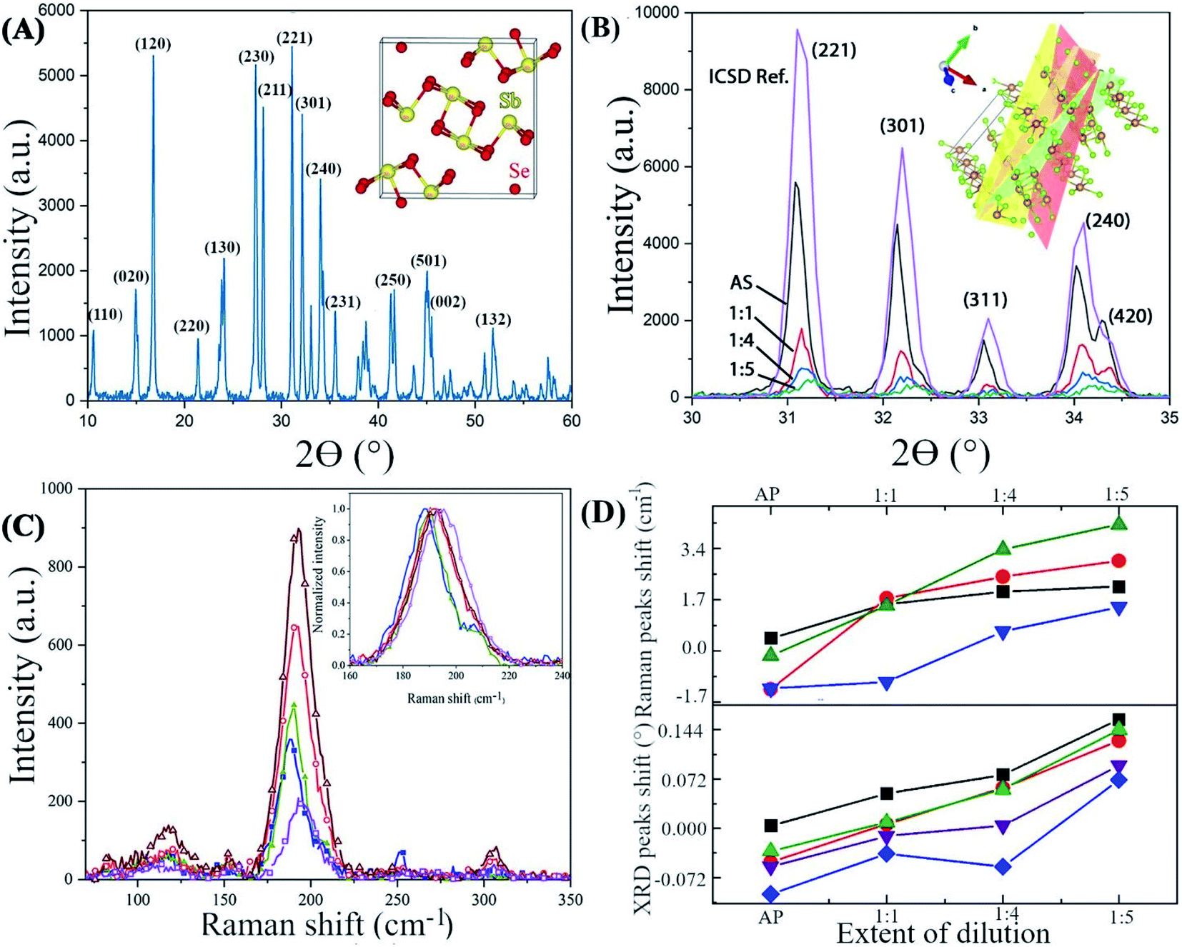 | ||
| Fig. 3 XRD and Raman spectra of antimony selenide nanowires (A) XRD and unit cell of antimony selenide projected through the (001) direction. (B) XRD pattern of shifted peaks corresponding to the (221), (301), (311), and (240) planes of antimony selenide nanowires deposited from solutions of varying en:EDT ratios. (C) Raman spectra of antimony selenide NWs deposited from solutions of varying en:EDT ratios. (D) Raman and XRD peak shifts versus extent of dilution. Raman peak shifts calculated for the Sb–Se vibrations (green; 188 cm−1), Se–Se vibrations (black, blue; 114 and 209 cm−1, respectively), and Sb–Sb vibrations (red; 150 cm−1) of antimony selenide NWs deposited from different en:EDT solvent mixtures. XRD peak shifts calculated for the (221) {black}, (301) {red}, (311) {green}, (204) {purple} and (420) {blue} lattice planes. | ||
| Sample name | ε (%) | ||||
|---|---|---|---|---|---|
| (221) | (301) | (311) | (240) | (420) | |
| a Calculated from XRD. | |||||
| AP | 0.03 | 0.07 | 0.03 | 0.02 | 0.07 |
| 1:1 |
0.12 | 0.26 | 0.09 | 0.15 | 0.1 |
| 1:4 |
0.21 | 0.26 | 0.23 | 0.19 | 0.05 |
| 1:5 |
0.45 | 0.47 | 0.48 | 0.43 | 0.41 |
The Raman spectra of the antimony selenide NWs consists of four characteristic Raman peaks at 114, 150, 188, and 209 cm−1 (Fig. 3C). The most intense peak, at 188 cm−1, is attributed to the Sb–Se stretching vibrations and is denoted as an Ag mode. The peaks at 114 and 209 cm−1 are associated with Se–Se vibrations (Ag), and the peak at 150 cm−1 corresponds to Sb–Sb vibrations (Au).33,34 Interestingly, as the en:EDT ratio of the solution increases, the Raman peaks of the corresponding antimony selenide NWs are shifted towards higher wavenumbers (Fig. 3D), which along with our XRD results, supports the presence of strain in the lattice. Therefore, the lattice strain correlates with the Se:Sb ratio. In contrast to these results, the XRD and Raman spectra of the antimony sulfide NWs did not show any appreciable peak shift when the en:EDT ratio of the corresponding precursor solution was increased (ESI Fig. S7 and S8†), albeit with significant deviation from stoichiometry.
Transmission electron microscopy confirms the correlation between the strain and the Se:Sb ratio (Fig. 4). A deformation in the lattice spacing near the tips of the NWs is apparent (indicated by the arrow in Fig. 4D), while a comparison of the Se:Sb ratio near the NWs tips, side edges, and interior indicate that the Se:Sb ratio is slightly lower near the tips than in the interior of the NWs (Table S4†). In addition, an amorphous layer (ca. 1.5 nm thick) is discernible at the NWs edges and tips (Fig. 4A, C, and D), and an amorphous layer with a 2–3 nm thickness is discernable at the grain boundaries of the NWs (Fig. 4E). Therefore, (i) the lattice strain correlates with the Se:Sb ratio (as was also observed with XRD and Raman spectroscopy), and (ii) the strain and the Se:Sb ratio is not uniform throughout the NWs. We further investigated the effects of these local and non-local variations on the local and non-local surface potential properties.
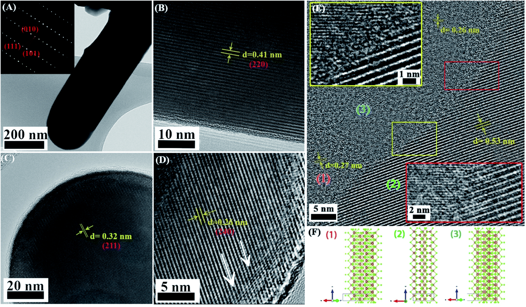 | ||
| Fig. 4 TEM of nanowires deposited on a carbon-coated grid. (A) Antimony selenide NW. The NW diameter is uniform over long distances. Inset: electron diffraction pattern; the sharp and periodic spots reflect the high crystallinity of the NWs. (B) TEM image of the side of a NW showing high crystallinity. (C) High magnification of the top of a NW shows high crystallinity up to ∼1.5 nm from the surface. The tips of the NWs are round-shaped. (D) High magnification of the tip of a NW shows the compression near the surface (en:EDT = 1:4). (E) FIB-TEM of grain boundaries (GBs). Three crystalline grains with different orientations form GBs with varying angles. An amorphous region with variable width is seen along the GB region of (2) and (3)—yellow and red boxed regions, respectively. (A)–(E) were taken from different NWs. The contrast in all figures was locally enhanced using the Fiji CALHE function. (F) Ball-and-stick structure of each crystalline domain projected along the direction of the grains in (E). (1), (2) and (3) are the projections of (301), (120) and (240) planes, respectively. | ||
We measured the contact potential difference (CPD), and surface photovoltage response (SPV) of antimony selenide NWs deposited from various en:EDT mixtures on FTO (Fig. 5). We found in all NWs a positive SPV value (CPDlight–CPDdark), suggesting that the NWs have p-type conductivity. In the dark, the CPD values of the NWs with a low Se:Sb ratio is more positive by ∼200 mV than the CPD value of the NWs with a near-stoichiometric ratio. This larger CPD reflects a larger work function, which indicates that the Fermi level in the NWs with a low Se:Sb is closer to the valence band maximum than in the NWs with a near-stoichiometric ratio.
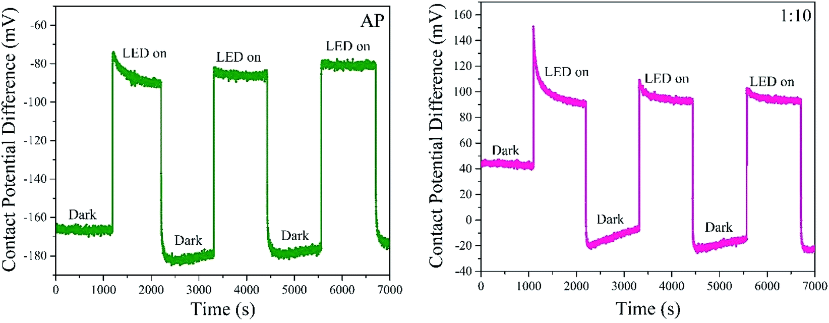 | ||
| Fig. 5 Surface photovoltage of antimony selenide NWs deposited from AP and 1:10 solutions. Contact potential difference of NWs prepared from AP and 1:10 solutions measured in dark and light conditions (illumination at 700 nm by LED photon source; indicated in the figure). | ||
An important difference between the samples prepared with a low Se:Sb ratio and those at near-stoichiometric Se:Sb ratio was found in the stabilization time after light excitation. For the NWs deposited with a nearly stoichiometric Se:Sb ratio (AP), the decay curve fits a monoexponential function with a characteristic decay parameter of τ = 277 ± 8 s. In contrast, for the NWs with a low Se:Sb ratio (1:10), a biexponential function is more suitable, and the decay time constants were τ1 = 40 ± 1 s and τ2 = 320 ± 10 s (however, the pre-exponential factor for τ2 was ten orders of magnitude larger than the one for τ1). Furthermore, in the second and third periods, the decay disappears in the AP sample, while it persists in the 1:10 sample. These differences indicate that trap states are more prevalent in the samples with a more significant deviation from stoichiometry. It also suggests that several trap sites with different characteristic trapping–detrapping kinetics exist in the stoichiometric and non-stoichiometric antimony selenide NWs.
We also carried out KPFM to probe the surface potential along the NWs and examine potential barriers at GBs. The surface potential across the GBs that are parallel to the nanowire axis (along the c-axis) varies by only a few millivolts (Fig. 6A and B) and is slightly less positive, indicating that the band bending at the GBs that are parallel to the nanowire axis (along c-axis) of antimony selenide is small. The bands bend slightly “upwards” (to less negative energy) near the boundary. A more significant surface potential variation is seen along the NWs than at GBs, with a positive change of 15–20 mV near the NW tip (Fig. 6D; we observed this effect in approximately one-third of the NWs in the AP sample). The more positive surface potential near the tips indicates a “downwards” (to more negative energy) bending of the energy levels near the tip. This result correlates with the TEM-EDS analysis (which shows a lower Se:Sb ratio near the tips of the NWs) and the CPD results (which indicate that NWs with a lower Se:Sb ratio have a larger work function).
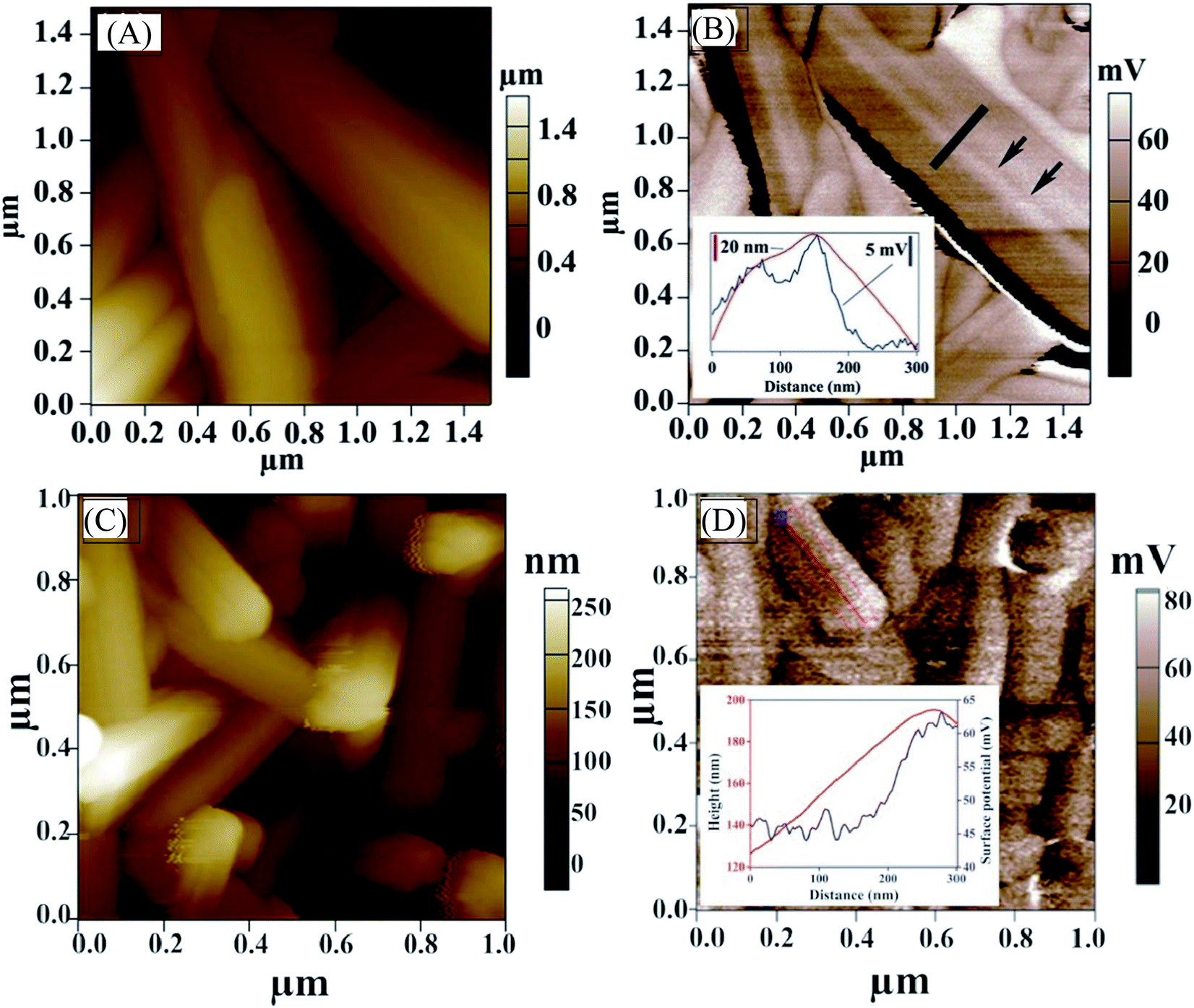 | ||
| Fig. 6 Kelvin probe force microscopy. (A) Topography AFM image of polycrystalline antimony selenide nanowires (NWs) prepared by deposition from an en:EDT solution (1:4 ratio). Black arrows indicate a grain boundary along the NW (001) crystal direction. (B) KPFM image of the same NW. The black arrows indicate a grain boundary; Inset: line profile of height difference (red) and contact potential difference (blue) across a grain boundary is shown. (C) Topography AFM image of antimony selenide NWs and (D) KPFM image of the same NWs. Surface potential is measured near the tip of a NW. Height difference (red) and surface potential variation (blue) are shown in the inset. The KPFM resolution is <20 nm, whereas the onset of the surface potential variation starts about 70 nm from the topographic onset of the edge (inset of Fig. 6D). Therefore, this change in surface potential is only slightly correlated with the topography of the NWs. | ||
Discussion
We investigated the effect of varying the en:EDT ratio on the micromorphology, stoichiometry, and optoelectronic properties of antimony selenide NWs prepared by spin coating followed by thermal treatment. We found that the Se:Sb ratio in the antimony selenide NW decreases as the en:EDT ratio increases and that the diameter of the NWs decreases as the fraction of en in the solvent mixture increases.
Brutchey and coworkers have shown that antimony metal is insoluble in the en:EDT solvent mixture without adding a chalcogen.20 Hence, the chalcogen facilitates the oxidation of antimony and its dissolution, but it is not yet clear if the reaction results in molecular species that contain both a chalcogen and Sb ions. It was also established that the addition of the amine ionizes the thiol groups.19,20 Park et al. used a mixture of 2-mercaptoethanol and en as a solvent to dissolve metallic antimony and selenide and found that regardless of the Se:Sb ratio used in the precursor ink, a nearly fixed Se:Sb ratio of ∼1.43 was found in the nanowires (NWs).35 In contrast, Deshmukh et al. have recently shown how the molecular structure of Se species varies with the thiol content and type if the amine content is changed after the dissolution.36 Our experience with thioglycolic acid shows that the Se:Sb ratio is affected by the en:EDT ratio (not shown). These observations suggest that at least for en:EDT mixtures, it is the structure of the molecular species that form after the dissolution and not the solubility of the different metals that affect the solid composition. This is supported by the results of our experiments with en:EDT or en added before the dissolution. We suggest that the addition of en facilitates splitting of the Sb-Sex species to smaller molecular weight species by increasing the thiolates concentration. A similar effect is obtained if the thiolates are added after the dissolution step (i.e., in the post-dissolution en:EDT series). This affects the crystallization process (e.g., by varying the molecular species' diffusion coefficient or evaporation rate), which eventually results in chalcogen deficiency and thinner NWs. Alternatively, specific adsorption of en or thiolates on the forming crystals' surface could limit the addition of Se and lead to non-stoichiometric solids. However, we did not study this phenomenon further; instead, we focused on identifying potential sources for the observed bandgap widening and studying the effects of varying the Se:Sb ratio in the NWs on their surface potential and surface photovoltaic response.
We consider what could be the leading causes for the widening of the optical bandgap. One may suggest that the apparent correlation with the decreasing NWs diameter could imply that quantum confinement plays a role.37 However, the reported Bohr radius of antimony selenide is ∼20 nm,38 whereas the typical diameter of the NW varies between 30 and 180 nm (Table 2). Therefore, while quantum confinement cannot be completely ruled out for the thinner NWs, confinement is unlikely in the thicker NWs, which also show a bandgap widening. Therefore, other mechanisms must be considered as well, such as alloying and strain. According to Vegard's law, for sulfur alloying (originating from the solvent thiols) to broaden the bandgap by 0.15 eV, a S:Se ratio of 1:1 is required.39 However, the NWs with the highest sulfur content (en:EDT 1:4 deposited on glass) still contained only 2.9 at% sulfur, which is insufficient to cause the observed bandgap broadening. The bandgap of semiconductors may also vary because of lattice strain, as reported in several works.40–42 XRD and Raman spectroscopy results suggest the presence of tensile strain in the antimony selenide NWs. Our results indicate a ∼0.48% strain. However, Liu et al. predicted that a ∼4% strain is needed to induce a ∼0.15 eV bandgap widening.43 Moreover, we also observed a widening of the bandgap in antimony sulfide NWs; their crystal structure is similar to antimony selenide, and their chalcogen:metal ratio follows a trend with respect to en:EDT ratio that is similar to the antimony selenide NWs. However, unlike for the antimony selenide NWs, we did not see any shift of the XRD and Raman peaks for the antimony sulfide NWs deposited from AP or diluted solutions (ESI Fig. S9 and S10†). Therefore, the strain contribution to the observed bandgap widening of the antimony selenide NWs is probably only minor.
Shaffer and coworkers investigated the effects of stoichiometric variation and crystallinity in evaporated thin films of antimony selenide and found that the optical absorption onset shifts when the Se:Sb ratio in the films is varied.44 Recently, Chen et al. compared the optical properties of crystalline and fully amorphous antimony selenide (i.e., with no apparent diffraction peaks); they found a shift in the optical absorption onset of the indirect bandgap from 1.03 eV for a crystalline film (accompanied by a 1.17 eV direct bandgap) to 1.39 eV for an amorphous film.45 In contrast to these previous reports, our NWs are not amorphous—diffraction was observed by both XRD and TEM even when the Se:Sb ratio was low. The lack of long-range order in amorphous antimony selenide was previously associated with the experimentally observed reduction in the density of states near the top of the valence band,46 which is formed chiefly from p orbitals of Se (with a minor contribution from s orbitals of Sb), due to a reduced orbitals overlap in the amorphous antimony selenide and weaker bonding. We propose that in antimony selenide NWs deposited from high en:EDT ratio inks, Se deficiency diminishes the density of states near the VBM, which manifests as optical bandgap broadening.
Our TEM-EDS investigation shows an uneven distribution of the Se:Sb ratio in the NWs near and away from the tip of the NWs. The correlation between the Se:Sb ratio and the optical bandgap suggest that the uneven distribution of Se and Sb leads to a grading of the optical bandgap from a high bandgap near the NWs tips to a smaller one away from the tip. In addition, the CPD measurements revealed a correlation between the Se:Sb ratio and the NWs work function, whereas KPFM studies indicated a higher surface potential near the tips of the NWs than away from it. In addition, we found a tiny band bending at grain boundaries parallel to the c-axis. The direction of the band bending indicates that photoexcited electrons are repelled from these grain boundaries. We conclude from these results that a band bending drifts photoexcited electrons toward the tip of the NWs. These two phenomena impact charge transport and recombination in thin-film PV and PEC devices using antimony selenide as a light absorber.
Conclusions
We tuned the composition of antimony selenide NWs by modifying the en:EDT solvent ratio. The induced changes in the Se:Sb ratio coincided with an increase in the optical bandgap (by up to ∼0.3 eV) and the work function (by ∼0.2 eV) in low Se:Sb ratio NWs in comparison to the nearly stoichiometric NWs. We suggest that due to Se deficiency the density of Se states near the valence band maximum diminishes and cause an apparent broadening of the bandgap. Lastly, we found that Se deficiency is not uniform along the NWs, which translates to a non-uniform surface potential along the NWs (as we confirmed by KPFM measurements). The suggested band bending towards the NWs tips is expected to cause photoexcited electrons to migrate towards the NWs tips. While the direct cause of the Se deficiency is not yet clear, based on the results presented in this work we suggest that the Sb–Se molecular species' structure is affected by the concentration of thiolates in the solution after the metals are dissolved. Since the optoelectronic effects are essential for photocathodes and photovoltaic devices engineering towards higher power conversion efficiencies, this work motivates future research to unravel the actual composition of the solutions that causes non-stoichiometry in the solids and for studying the optoelectronic effects on photocatalytic processes.
Conflicts of interest
There are no conflicts to declare.Acknowledgements
We thank the Israeli Ministry of Energy and Infrastructure for the support of the research through grant no. 218-11-031 and Ben-Gurion University support through startup grant. We are particularly grateful to Dr Vladimir Ezersky for carrying out HRTEM and supporting analysis, Dr Mariela Pavan for performing Raman spectroscopy measurements, Juergen Jopp for KPFM measurements, Dr Natalya Froumin for performing XPS, and Sumesh Sadhujan for his help with the SPV measurements. EE is thankful to Professor David Cahen for a fruitful discussion, Professor Rachel Yerushalmi-Rosen for critically reviewing the manuscript and productive suggestions, and Dr Muhammad Bashouti for granting us access to SPV measurements.References
- Y. Zhou, M. Leng, Z. Xia, J. Zhong, H. Song, X. Liu, B. Yang, J. Zhang, J. Chen, K. Zhou, J. Han, Y. Cheng and J. Tang, Adv. Energy Mater., 2014, 4, 1301846 CrossRef.
- C. Chen, D. C. Bobela, Y. Yang, S. Lu, K. Zeng, C. Ge, B. Yang, L. Gao, Y. Zhao, M. C. Beard and J. Tang, Front. Optoelectron., 2017, 10, 18–30 CrossRef.
- Y. Zhou, L. Wang, S. Chen, S. Qin, X. Liu, J. Chen, D.-J. Xue, M. Luo, Y. Cao, Y. Cheng, E. H. Sargent and J. Tang, Nat. Photonics, 2015, 9, 409–415 CrossRef CAS.
- Z. Li, X. Liang, G. Li, H. Liu, H. Zhang, J. Guo, J. Chen, K. Shen, X. San, W. Yu, R. E. I. Schropp and Y. Mai, Nat. Commun., 2019, 10, 125 CrossRef PubMed.
- R. Tang, X. Wang, W. Lian, J. Huang, Q. Wei, M. Huang, Y. Yin, C. Jiang, S. Yang, G. Xing, S. Chen, C. Zhu, X. Hao, M. A. Green and T. Chen, Nat. Energy, 2020, 5, 587–595 CrossRef CAS.
- T. D. C. Hobson, O. S. Hutter, M. Birkett, T. D. Veal and K. Durose, in 2018 IEEE 7th World Conference on Photovoltaic Energy Conversion (WCPEC) (A Joint Conference of 45th IEEE PVSC, 28th PVSEC & 34th EU PVSEC), IEEE, 2018, pp. 0818–0822 Search PubMed.
- M. Birkett, W. M. Linhart, J. Stoner, L. J. Phillips, K. Durose, J. Alaria, J. D. Major, R. Kudrawiec and T. D. Veal, APL Mater., 2018, 6, 084901 CrossRef.
- C. H. Don, H. Shiel, T. D. C. Hobson, C. N. Savory, J. E. N. Swallow, M. J. Smiles, L. A. H. Jones, T. J. Featherstone, P. K. Thakur, T.-L. Lee, K. Durose, J. D. Major, V. R. Dhanak, D. O. Scanlon and T. D. Veal, J. Mater. Chem. C, 2020, 8, 12615–12622 RSC.
- W. Yang and J. Moon, J. Mater. Chem. A, 2019, 7, 20467–20477 RSC.
- W. Yang, J. Park, H. C. Kwon, O. S. Hutter, L. J. Phillips, J. Tan, H. Lee, J. Lee, S. D. Tilley, J. D. Major and J. Moon, Energy Environ. Sci., 2020, 13, 4362–4370 RSC.
- W. Yang, J. Ahn, Y. Oh, J. Tan, H. Lee, J. Park, H. C. Kwon, J. Kim, W. Jo, J. Kim and J. Moon, Adv. Energy Mater., 2018, 8, 1–11 Search PubMed.
- T. T. Ngo, S. Chavhan, I. Kosta, O. Miguel, H.-J. Grande and R. Tena-Zaera, ACS Appl. Mater. Interfaces, 2014, 6, 2836–2841 CrossRef CAS PubMed.
- M. B. Costa, F. W. S. Lucas and L. H. Mascaro, ChemElectroChem, 2019, 6, 2937–2944 CrossRef CAS.
- Y. Rodríguez-Lazcano, Y. Peña, M. T. S. Nair and P. K. Nair, Thin Solid Films, 2005, 493, 77–82 CrossRef.
- D. B. Mitzi, Adv. Mater., 2009, 21, 3141–3158 CrossRef CAS.
- C. H. Chung, B. Lei, B. Bob, S. H. Li, W. W. Hou, H. S. Duan and Y. Yang, Chem. Mater., 2011, 23, 4941–4946 CrossRef CAS.
- B. Yang, D. J. Xue, M. Leng, J. Zhong, L. Wang, H. Song, Y. Zhou and J. Tang, Sci. Rep., 2015, 5, 1–11 CAS.
- C. L. McCarthy and R. L. Brutchey, Chem. Commun., 2017, 53, 4888–4902 RSC.
- D. H. Webber and R. L. Brutchey, J. Am. Chem. Soc., 2013, 135, 15722–15725 CrossRef CAS PubMed.
- D. H. Webber, J. J. Buckley, P. D. Antunez and R. L. Brutchey, Chem. Sci., 2014, 5, 2498 RSC.
- C. L. McCarthy, D. H. Webber, E. C. Schueller and R. L. Brutchey, Angew. Chem., Int. Ed., 2015, 54, 8378–8381 CrossRef CAS PubMed.
- Z. Lin, Q. He, A. Yin, Y. Xu, C. Wang, M. Ding, H. C. Cheng, B. Papandrea, Y. Huang and X. Duan, ACS Nano, 2015, 9, 4398–4405 CrossRef CAS PubMed.
- B. C. Walker and R. Agrawal, Chem. Commun., 2014, 50, 8331–8334 RSC.
- C. L. McCarthy, C. A. Downes and R. L. Brutchey, Inorg. Chem., 2017, 56, 10143–10146 CrossRef CAS PubMed.
- X. Zhao, R. Zhang, C. Handwerker and R. Agrawal, in 2016 IEEE 43rd Photovoltaic Specialists Conference (PVSC), IEEE, 2016, pp. 0542–0544 Search PubMed.
- X. Zhao, S. D. Deshmukh, D. J. Rokke, G. Zhang, Z. Wu, J. T. Miller and R. Agrawal, Chem. Mater., 2019, 31, 5674–5682 CrossRef CAS.
- C. L. McCarthy and R. L. Brutchey, Dalton Trans., 2018, 47, 5137–5143 RSC.
- S. D. Deshmukh, R. G. Ellis, D. S. Sutandar, D. J. Rokke and R. Agrawal, Chem. Mater., 2019, 31, 9087–9097 CrossRef CAS.
- Z. Ma, S. Chai, Q. Feng, L. Li, X. Li, L. Huang, D. Liu, J. Sun, R. Jiang, T. Zhai and H. Xu, Small, 2019, 15, 1–8 Search PubMed.
- P. D. Fochs, Proc. Phys. Soc., London, Sect. B, 1956, 69, 70–75 CrossRef.
- H. W. Seo, S. Y. Bae, J. Park, H. Yang, K. S. Park and S. Kim, J. Chem. Phys., 2002, 116, 9492–9499 CrossRef CAS.
- M. Selvaraj, V. Venkatachalapathy, J. Mayandi, S. Karazhanov and J. M. Pearce, AIP Adv, 2015, 5, 117119 CrossRef.
- A. Shongalova, M. R. Correia, J. P. Teixeira, J. P. Leitão, J. C. González, S. Ranjbar, S. Garud, B. Vermang, J. M. V. Cunha, P. M. P. Salomé and P. A. Fernandes, Sol. Energy Mater. Sol. Cells, 2018, 187, 219–226 CrossRef CAS.
- P. Vidal-Fuentes, M. Guc, X. Alcobe, T. Jawhari, M. Placidi, A. Pérez-Rodríguez, E. Saucedo and V. I. Roca, 2D Mater., 2019, 6, 045054 CrossRef CAS.
- J. Park, W. Yang, Y. Oh, J. Tan, H. Lee, R. Boppella and J. Moon, ACS Energy Lett., 2019, 4, 517–526 CrossRef CAS.
- S. D. Deshmukh, L. F. Easterling, J. M. Manheim, N. J. LiBretto, K. G. Weideman, J. T. Miller, H. I. Kenttämaa and R. Agrawal, Inorg. Chem., 2020, 59, 8240–8250 CrossRef CAS PubMed.
- S. A. Goudsmit, Phys. Rev. Lett., 1960, 5, 233 CrossRef.
- N. N. Syrbu, V. V. Zalamai, I. G. Stamov and S. I. Beril, Beilstein J. Nanotechnol., 2020, 11, 1045–1053 CrossRef CAS PubMed.
- Z. Deng, M. Mansuripur and A. J. Muscat, Nano Lett., 2009, 9, 2015–2020 CrossRef CAS PubMed.
- R. W. Shao, K. Zheng, B. Wei, Y. F. Zhang, Y. J. Li, X. D. Han, Z. Zhang and J. Zou, Nanoscale, 2014, 6, 4936–4941 RSC.
- L. Yang, X. Cui, J. Zhang, K. Wang, M. Shen, S. Zeng, S. A. Dayeh, L. Feng and B. Xiang, Sci. Rep., 2014, 4, 1–7 CAS.
- S. B. Desai, G. Seol, J. S. Kang, H. Fang, C. Battaglia, R. Kapadia, J. W. Ager, J. Guo and A. Javey, Nano Lett., 2014, 14, 4592–4597 CrossRef CAS PubMed.
- W. Liu, X. Peng, C. Tang, L. Sun, K. Zhang and J. Zhong, Phys. Rev. B: Condens. Matter Mater. Phys., 2011, 84, 1–5 Search PubMed.
- C. Wood, Z. Hurych and J. C. Shaffer, J. Non. Cryst. Solids, 1972, 8–10, 209–214 CrossRef CAS.
- C. Chen, W. Li, Y. Zhou, C. Chen, M. Luo, X. Liu, K. Zeng, B. Yang, C. Zhang, J. Han and J. Tang, Appl. Phys. Lett., 2015, 107, 043905 CrossRef.
- Z. Hurych, D. Buczek, C. Wood, G. J. Lapeyre and A. D. Baer, Solid State Commun., 1973, 13, 823–827 CrossRef CAS.
Footnote |
| † Electronic supplementary information (ESI) available. See DOI: 10.1039/d1na00814e |
| This journal is © The Royal Society of Chemistry 2022 |