
 Open Access Article
 This Open Access Article is licensed under a
 Creative Commons Attribution 3.0 Unported Licence
Fabry–Perot interferometric calibration of van der Waals material-based nanomechanical resonators†
Myrron Albert
Callera Aguila‡
 *abc,
Joshoua Condicion
Esmenda‡
*abc,
Jyh-Yang
Wang
c,
Teik-Hui
Lee
c,
Chi-Yuan
Yang
c,
Kung-Hsuan
Lin
c,
Kuei-Shu
Chang-Liao
a,
Sergey
Kafanov
d,
Yuri A.
Pashkin
d and
Chii-Dong
Chen
*c
*abc,
Joshoua Condicion
Esmenda‡
*abc,
Jyh-Yang
Wang
c,
Teik-Hui
Lee
c,
Chi-Yuan
Yang
c,
Kung-Hsuan
Lin
c,
Kuei-Shu
Chang-Liao
a,
Sergey
Kafanov
d,
Yuri A.
Pashkin
d and
Chii-Dong
Chen
*c
aNational Tsing Hua University, Hsinchu 30013, Taiwan. E-mail: maguila@gate.sinica.edu.tw
bNano Science and Technology Program, Taiwan International Graduate Program, Academia Sinica and National Tsing Hua University, Taiwan
cInstitute of Physics, Academia Sinica, Nangang 11529, Taiwan. E-mail: chiidong@phys.sinica.edu.tw
dDepartment of Physics, Lancaster University, Lancaster LA1 4YB, UK
First published on 23rd November 2021
Abstract
One of the challenges in integrating nanomechanical resonators made from van der Waals materials in optoelectromechanical technologies is characterizing their dynamic properties from vibrational displacement. Multiple calibration schemes using optical interferometry have tackled this challenge. However, these techniques are limited only to optically thin resonators with an optimal vacuum gap height and substrate for interferometric detection. Here, we address this limitation by implementing a modeling-based approach via multilayer thin-film interference for in situ, non-invasive determination of the resonator thickness, gap height, and motional amplitude. This method is demonstrated on niobium diselenide drumheads that are electromotively driven in their linear regime of motion. The laser scanning confocal configuration enables a resolution of hundreds of picometers in motional amplitude for circular and elliptical devices. The measured thickness and spacer height, determined to be in the order of tens and hundreds of nanometers, respectively, are in excellent agreement with profilometric measurements. Moreover, the transduction factor estimated from our method agrees with the result of other studies that resolved Brownian motion. This characterization method, which applies to both flexural and acoustic wave nanomechanical resonators, is robust because of its scalability to thickness and gap height, and any form of reflecting substrate.
Nanomechanical resonators (NMRs) made from van der Waals materials like graphene1–3 and transition metal dichalcogenides4–7 offer plausible platforms for measuring minuscule forces3,8 and ultralight masses9 with unprecedented sensitivity and motion responsivity5,7,10 to external stimuli. Typical NMR-based sensing platforms involve monitoring changes in features of the driven frequency response, primarily the shifts of the mechanical frequency and variations of the linewidth, in the presence of an actuating force.11 The calibrated vibrational amplitude at resonance, together with the resonator frequency, provides direct quantification of the Young's elastic modulus, effective mass, and driving force felt by the NMR from a single response spectrum.12 From a practical standpoint, monitoring the vibrational amplitude is essential for avoiding dynamic pull-in instability13 when driving the NMR at high amplitude, which limits the actuation ranges for electromotively driven NMRs. Furthermore, the vibrational resonant amplitude enables understanding of the nonlinear regime of motion14,15 and optomechanical effects on driven mechanics,8,16,17 both of which are accessible for mechanical resonators with nanoscale dimensions, and embedded in motion-sensitive interferometric platforms.
Calibration of the motional amplitude of NMRs using Fabry–Perot (FP) interferometry has been challenging because it requires pre-determination of device parameters such as thickness and spacer gap, which are difficult to ascertain and vary from device to device. Previous attempts of this calibration were shown through the resolving of the Brownian motion,7,18,19 analyzing the high-amplitude Duffing response,3 measuring the driven motion at higher harmonics,20 and monitoring photodetector responses.12 The calibration methods used in these previous studies, however, rely on specific device conditions such as optically transparent cross-sections,2,7 access to high amplitude nonlinear motion, and high optical-to-displacement responsivities10 from an optimal vacuum gap. These characteristics are specific to monolayer, bilayer, trilayer, and few-layer van der Waals materials, whose unique optical characteristics, ultralight mass, and mechanics more closely resemble near-transparent, prestressed membranes. The methods would not be accurate if one or several of these criteria are not met.
Also, there are applications where a smaller vacuum gap between the NMR and the substrate has advantages over the optimal gap for interferometric detection. These include large frequency tunability in electromotively driven NMRs,9,21 stronger electromechanical coupling between NMR and microwave cavities,8,16 and introducing optomechanics in an electromechanical system.22–24 For these applications, van der Waals materials of intermediate thickness (between 10 L and 100 L) offer comparable (if not better) optical reflectance-to-displacement responsivity10 and electromechanical coupling,8,14,16,25 and near strain-free mechanical frequencies26 as compared to their few-layer counterparts. Furthermore, they are easier to prepare via micromechanical exfoliation, and polymeric contaminants have a negligible contribution to their masses.
In this work, we show that the motion of an NMR can be calibrated by considering multilayer wave interference occurring on FP structures. To demonstrate the robustness of the technique, a thick van der Waals material, 2H-NbSe2, is used as the drumhead. 2H-NbSe2, at room temperature, is a semi-metallic material, whose number of layers, when increased, is difficult to differentiate with Raman spectroscopy signatures27 from the bulk, unlike MoS2.28 This material makes it a unique model for assessing the number of layers based on the layer-dependent refractive index. Our approach, implemented with laser scanning confocal microscopy, allows robust, non-contact and in situ determination of the layer thickness, spacer height, and device responsivity of each translucent flexible mirror. Our calibration scheme, using a 532 nm laser wavelength, reveals a subnanometer displacement response of NMRs with thickness exceeding 50 nm. Furthermore, calibrated spatial imaging of the driven fundamental mode of circular and elliptical NbSe2 drums enables direct investigation of the modal properties (i.e. effective mass and Young's elastic modulus) of the drumheads.
Experimental
Device fabrication
P-type doped Si chips (7 mm × 7 mm × 0.65 mm), with a thermally grown 543 nm thick SiO2 layer, were lithographically patterned with 20 nm Cr and 40 nm Au electrodes. The chips are cleaned, and then spin-coated with a CSAR-62 electron-beam resist to create the spacer. The resist is exposed in an electron-beam writer with drum holes and contact window patterns. After the development, the resist is baked at 180 °C for 9 minutes to harden the spacer. The spacer thickness, as measured with a commercial stylus profilometer, is 295 ± 10 nm. Bulk NbSe2 flakes purchased from HQ Graphene are exfoliated and transferred onto the patterned drum and contact windows using a dry polydimethylsiloxane stamp transfer process. Additional details on the flake transfer process are narrated in other studies.29,30Electromotive actuation and interferometric detection
The sample is placed in a vacuum box at ambient temperature (20–22 °C), with optical and electrical access, which is evacuated to a base pressure of 6 × 10⁻⁷ mbar to minimize viscous losses. The NbSe2 flake is galvanically connected to the output of the function generator, which creates DC and AC voltages between the flake and the grounded Au/Cr electrode forming a parallel-plate capacitor. This voltage produces an attractive force between the capacitor plates, which actuates the drums when the driving frequency matches the resonance frequency. The drums experience an electromotive force arising from the DC and AC voltage inputs of the function generator. A custom-built confocal microscope, with a continuous wave 532 nm laser (Lighthouse Photonics Sprout-G) and a spot size of roughly 1.9 μm, probes the out-of-plane position and motional amplitude of the drums interferometrically. A fast avalanche photodetector (Thorlabs APD130A/M) measures both the average and modulated intensities of light reflected from the drums, and converts them to the output voltages![[V with combining macron]](https://www.rsc.org/images/entities/i_char_0056_0304.gif) and Ṽ. The data acquisition (DAQ) system records at coordinates of X and Y. A high-frequency lock-in amplifier (Stanford Research SRS-844) processes Ṽ with the signal frequency referenced from the function generator. See Fig. S1† for a detailed schematic diagram of the interferometer setup.
and Ṽ. The data acquisition (DAQ) system records at coordinates of X and Y. A high-frequency lock-in amplifier (Stanford Research SRS-844) processes Ṽ with the signal frequency referenced from the function generator. See Fig. S1† for a detailed schematic diagram of the interferometer setup.
Results and discussion
Determination of the thickness and vacuum gap via optical contrast
Fig. 1(a) shows device A, a circular drum with a hole diameter of 7 μm, and device B, an elliptical drum with hole diameters of 8 μm (X, major axis) and 7 μm (Y, minor axis). The devices share the same flake, ground electrode, and driving voltages. The NbSe2 flake and ground electrodes are separated by an insulating layer (electron-beam resist CSAR-62) and vacuum spacers, and hence form Fabry–Perot cavities for detection, and capacitors for actuation. A large rectangular opening, located tens of microns below the drum centers, allows the flake to connect to the voltage-controlled Au/Cr electrodes. The motion of the electromotively driven drumheads is detected interferometrically in a high vacuum environment. | ||
| Fig. 1 (a) Optical micrograph of the NbSe2 plate resonator devices. The circuit diagram shows the electromotive scheme used in driving the resonator. (b) Schematic drawing of the optical cross-section of the device (zones 3 and 4) and the references (zones 1 and 2) as measured via Fabry–Perot interference. The actuation circuit is added for clarity. (c) Confocal image showing devices A and B as scanned with a probe laser beam with wavelength λ = 532 nm. Scale bars in (a) and (c) are set to 10 μm. (d) Sketch of the output voltage of the fast photodetector versus time of a driven flexural resonator. | ||
Our method relies on different contrasts of light elastically reflected from each zone, as shown in Fig. 1(b). The flake (pink bar) acts as a translucent movable mirror with thickness h, which is separated from the ground electrode by a spacer of height s. For convenience, the reflected intensity is expressed in terms of reflectance R, which is the ratio of the total reflected light intensity to the incident intensity. Stationary mirrors have only DC component R = ![[R with combining macron]](https://www.rsc.org/images/entities/i_char_0052_0304.gif) , while movable mirrors have both and AC component
, while movable mirrors have both and AC component ![[R with combining tilde]](https://www.rsc.org/images/entities/i_char_0052_0303.gif) . Zones 1 and 2 represent two stationary mirrors: stacks of gold, orange, green and blue bars having reflectance R1 = 1 and a mirror covered with a spacer (light gray) having reflectance R2 = 2, respectively. Zone 3 represents two stationary mirrors separated by a dielectric gap (clamp) with reflectance R3 = 3. Finally, zone 4 is the main FP cavity composed of one stationary and one movable mirror, which are separated by a vacuum gap with reflectance R4. Here, zones 1 and 2 are references for zones 4 and 3, respectively. Scanning mirrors in the measurement setup move the laser spot in each zone a distance X and Y away from the center of the drums.
. Zones 1 and 2 represent two stationary mirrors: stacks of gold, orange, green and blue bars having reflectance R1 = 1 and a mirror covered with a spacer (light gray) having reflectance R2 = 2, respectively. Zone 3 represents two stationary mirrors separated by a dielectric gap (clamp) with reflectance R3 = 3. Finally, zone 4 is the main FP cavity composed of one stationary and one movable mirror, which are separated by a vacuum gap with reflectance R4. Here, zones 1 and 2 are references for zones 4 and 3, respectively. Scanning mirrors in the measurement setup move the laser spot in each zone a distance X and Y away from the center of the drums.
Application of DC and AC voltages to the flake exerts an attractive force; the NMR responds with an out-of-plane motional amplitude z at a driving frequency fd. Due to the position and motion of the movable mirror in zone 4, the main FP cavity has reflectance R4 = 4 + 4(fd), with 4 ≫ 4(fd). Fig. 1(d) shows the photodetector output signal V acquired from R4. Both the DC component and the AC component Ṽ of the output signal are proportional to 4 and 4, respectively. Amplitude z is determined after obtaining h and s.
Though we calculate 1–4 using the multilayer interference approach31–33 (MIA), the reflectance of FP cavities with four interfaces343,4 captures the stationary reflections occurring for each drum. Here, we assume that the coherent probe light, having wavelength λ, originates from a point source and propagates from a semi-infinite vacuum layer. The drum and the bottom mirror have complex refractive indices ![[n with combining circumflex]](https://www.rsc.org/images/entities/i_char_006e_0302.gif) h (ref. 27) and m, respectively, while the spacers have real refractive index s (s,drum for the vacuum spacer and s,clamp for the CSAR-62 spacer). In this geometry, the vacuum–NMR, NMR–spacer, and spacer–mirror interfaces contribute significantly to the cavity's overall reflectance. The total reflectance is defined as
h (ref. 27) and m, respectively, while the spacers have real refractive index s (s,drum for the vacuum spacer and s,clamp for the CSAR-62 spacer). In this geometry, the vacuum–NMR, NMR–spacer, and spacer–mirror interfaces contribute significantly to the cavity's overall reflectance. The total reflectance is defined as
 | (1) |
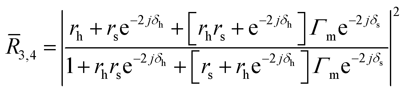
hh/λ is the optical phase thickness of the NMR, δs = 2πss/λ is the optical phase thickness of the spacer, rh = (1 − h)/(1 + h) is the Fresnel coefficient of the vacuum–NMR interface, rs = (h − s)/(h + s) is the Fresnel coefficient of the NMR–spacer interface, and Γm = (s − m)/(s + m) is the equivalent Fresnel coefficient of the spacer–mirror interface. For convenience, Γm is computed using MIA.†
Fig. 1(c) shows the confocal image constructed from the DC voltage of the photodetector. The image reveals the topographical features of the drum and its surroundings. The measured voltages that correspond to zones 1 and 2, mentioned in Fig. 1(b), are taken from the areas shown with the arrows in Fig. 1(c) and they are represented by 1 and 2, respectively. Following the white dashed line in Fig. 1(c), the measured voltage outside the boundary is defined by 3, while the measured voltage inside is represented by 4. It is important to note that the mismatch between the drum boundaries in Fig. 1(a) and (c) is caused by the deformation of the edge of the drum holes during the elastomeric stamp step of the flake transfer.
Since is susceptible to scattering losses,35 we circumvent this issue by normalizing the Michelson contrast34,36 of each FP cavity to its reference. Having defined the experimental and calculated reflectance, the cavity's optical contrast, C, is quantified as C = (3,4 − 2,1)/(3,4 + 2,1), where 3,4 is the stationary reflectance of the FP cavity, and 2,1 is the stationary reflectance of the cavity's reference. Apparently, C ranges between −1 and 1, with zero denoting no difference from the reference. If C is positive, then the cavity is brighter than the reference. Otherwise, the cavity is darker than its reference.
The output voltages measured for each pixel along the dashed lines in Fig. 1(c) are converted into contrast values for devices A and B, as depicted in Fig. 2(a). The experimental contrast Cexp represents the ratio of voltages acquired from different zones in the confocal image of each device while the modelled contrast Cmod is derived using MIA.† See Fig. S5† for the correspondence between the modelled contrast and its h and s pairs for devices A and B. Fig. 2(b and c) show the resulting h and s cross-sectional profiles acquired from minimizing the difference between the experimental contrast values and the contrasts generated by MIA. The mean resonator thicknesses and spacer heights are in excellent agreement with the mean values listed in Table 1. The thickness of the drums measured by our method agrees well with atomic force microscopy measurements for different areas of the flake, as shown in Fig. S2.† The spacer height for both drums and clamps agrees well with the stylus profilometer measurements. From the flake thickness of about 55 nm, we deduce 92 layers of NbSe2 sheets assuming a single layer thickness of 0.6 nm.37
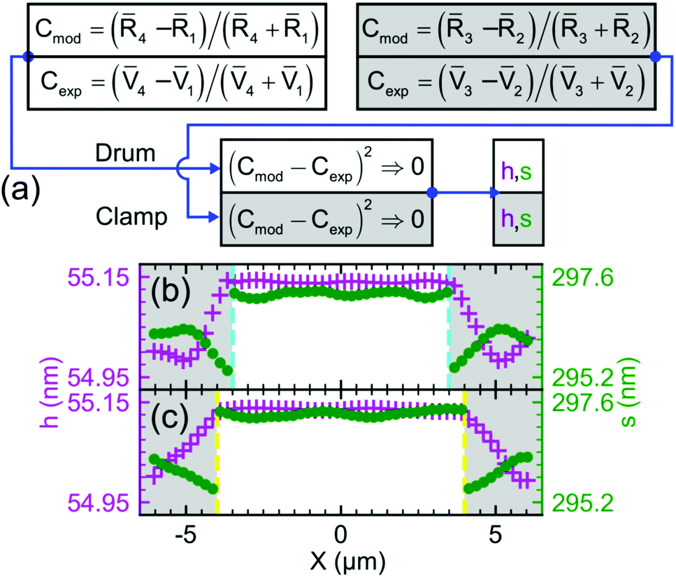 | ||
| Fig. 2 (a) Diagram for determining h and s for the clamp and drum zones. Minimization of the difference between the experimental contrast (Cexp) and the modelled contrast (Cmod) results in h and s profiles for device A (b) and device B (c). Colored dashed lines refer to the hole radius set in Fig. 1(a and c), separating the drum (white fills) and clamp (gray fills) zones. | ||
| Devices | A | B |
|---|---|---|
| h drum (nm) | 55.139 ± 0.002 | 55.135 ± 0.002 |
| h clamp (nm) | 55.03 ± 0.05 | 55.05 ± 0.04 |
| s drum (nm) | 297.2 ± 0.1 | 297.3 ± 0.1 |
| s clamp (nm) | 296.0 ± 0.3 | 295.9 ± 0.3 |
The h profiles in Fig. 2(b and c) show a hundred picometer variation between the drum and clamp zones. Meanwhile, buckling is observed in the s profiles in Fig. 2(b and c) as sdrum for both devices is greater than sclamp by 1.2–1.4 nm. We see the drumheads bulge38–40 presumably due to the pressure difference between the trapped air in the drum hole and the vacuum environment. The surface roughness of the movable mirror likely originates from the thermally grown oxide41 on the surface of the stationary mirror.
Conversion of optical signals to motional amplitudes
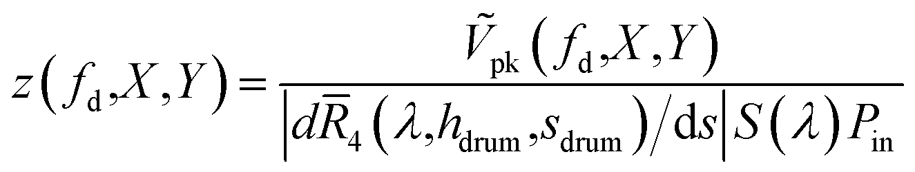
Having determined the mean hdrum and sdrum, we evaluate the optical reflectance-to-displacement responsivity |d4/ds| of each drum. This quantity is obtained from 4(fd) = |d4/ds|z(fd). The AC component reflected from zone 4 and characterized by 4, being purely due to mechanical motion, is insensitive to any scattering losses as this wave is amplitude-modulated. Eqn (1) is then corrected by a prefactor of 0.28 that accounts for the 1.9 μm spot diameter of the probe Gaussian beam. See Fig. S3(a)† for more details on the scaling prefactor.
Estimation of |d4/ds| requires the calculation of the gradient of the corrected 4 with respect to s. Fig. 3(a) shows 4 and its gradient as functions of s. As our NbSe2 plate is considered bulk,27 the 4versus s dependence shows a periodic yet non-sinusoidal behaviour. Yet, this dependence exhibits λ/2 periodicity, though the peak-to-dip and dip-to-peak spacings are asymmetric. The minima and maxima in the |d4/ds| versus s response are shifted by about ±λ/12 with respect to the dip in 4versus s, deviating from the periodic λ/4 spacing expected for FP cavities with a partially transparent moving mirror. We also find that the 4versus s dependence for a monolayer NbSe2 flake follows a distorted, sinusoidal behaviour as shown in Fig. S4(a).† This is unlike the regular sinusoid shape for those mechanical resonators of optically thin cross-sections.2,7 Evaluating |d4/ds| at s = sdrum (black dotted line) yields a device responsivity of 0.40 × 10⁻³ nm−1.
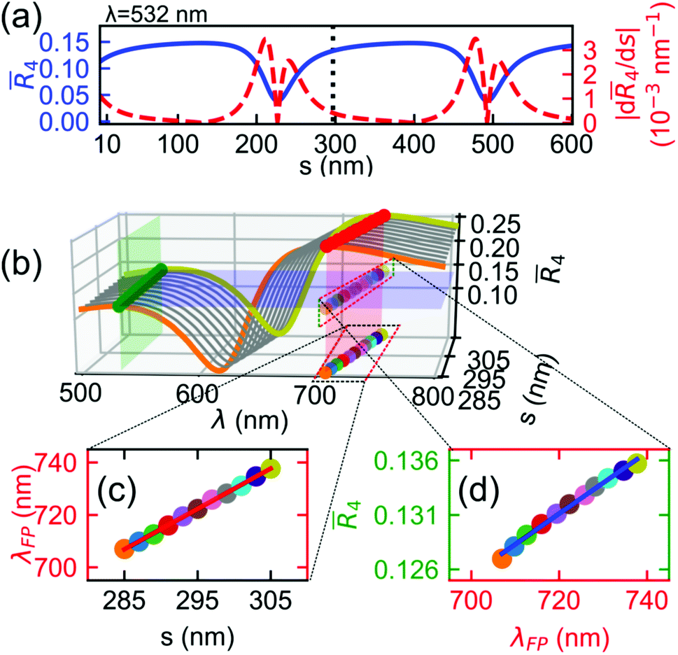 | ||
| Fig. 3 (a) Calculated reflectance 4 and device responsivity |d4/ds| vs. vacuum spacer height s of the measured FP device evaluated at h = 55 nm and λ = 532 nm. (b) Waterfall plot of FP reflectance as a function of λ at varying s, with the used probe wavelength (green plane) situated at λ = 532 nm. (c) Colored scatter plot of λFP as a function of s. The slope of the red solid line originates from the intersection of the red plane with the λ − s plane in (b). (d) Colored scatter plot of 4 as a function of the cavity shift λFP. The blue solid line originates from the intersection of the blue plane with the red plane in (b). | ||
We define the average |d4/ds| to account for spatial variations in sdrum across the plate due to the pressure difference and DC voltage. Note that each complex-valued refractive index is dependent on the probing wavelength; this translates to the wavelength-dependent rh, rs and Γm. We modeled |d4/s|avg. by the chain rule |Δ4(λ)/ΔλFP‖ΔλFP/Δs|s = sdrum, where Δ4/ΔλFP is the change of 4 with regards to the wavelength shift in the FP cavity, and ΔλFP/Δs is the wavelength shift of the FP cavity caused by the change of the spacer gap. Here, we define λFP as the wavelength at which 4(λ) is maximum in the range of λ = 500–900 nm. The resulting dependences are shown as a waterfall plot in Fig. 3(b) with a gap range exceeding the uncertainty of our stylus profilometer. Fig. 3(b) demonstrates larger 4 at near-infrared wavelengths. Fig. 3(c) shows the peak wavelength of the cavity, falling in the near-infrared range, shifting linearly with a slope of 1.543 nm/nm as sdrum increases from 285 nm to 305 nm. Fig. 3(d) shows how the shift consequently increases 4(λ) linearly, with a slope of 0.28 × 10⁻⁶ nm−1. The product of these two slopes, |d4/ds|avg = 0.43 × 10⁻³ nm−1, agrees with the evaluation in Fig. 3(a). The continuous behaviour seen in Fig. 3(b and c) is different from the discontinuous dependence observed for thin membranes in the same ranges of s, as shown in Fig. S4(b–d).† Their difference is mainly due to sharper features of the device responsivity of thin membranes as compared to thicker plates.
We use the average responsivity together with the interferometer system gain S(λ) (V/W) (see the ESI† for more detailed calculations) and the laser probe power Pin to define the displacement amplitude z as
 | (2) |
 factors of 0.20 μV pm−1 for device A and 0.22 μV pm−1 for device B for probe powers listed in Fig. 4(a and b).
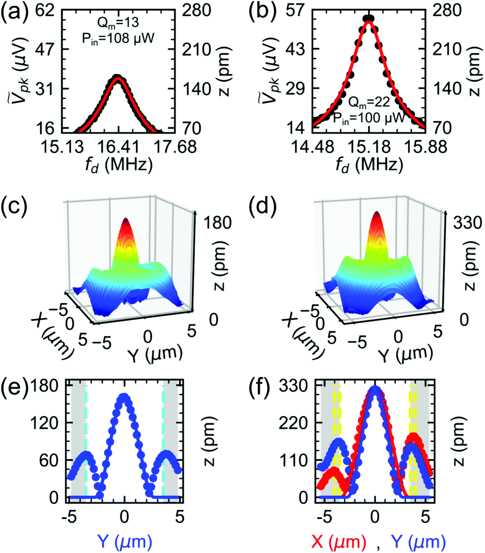 | ||
Fig. 4 Spot-based displacement amplitude response ( ) of device A (a) and device B (b) at VDC = 4 V and VAC = 125 mV and their driven resonator fits (red solid lines). The data shown in (c) and (d) refer to the spatial amplitude mode shape of devices A and B at fd = fm. The amplitude profiles along X ( ) of device A (a) and device B (b) at VDC = 4 V and VAC = 125 mV and their driven resonator fits (red solid lines). The data shown in (c) and (d) refer to the spatial amplitude mode shape of devices A and B at fd = fm. The amplitude profiles along X ( ) and Y ( ) and Y ( ) axes of the mode shapes for devices A (e) and B (f) are fitted with a clamped circular plate model (red and blue solid lines for X and Y, respectively). Dashed vertical lines indicate the edges of the holes. ) axes of the mode shapes for devices A (e) and B (f) are fitted with a clamped circular plate model (red and blue solid lines for X and Y, respectively). Dashed vertical lines indicate the edges of the holes. | ||
Calibration of motional amplitude in the frequency and spatial domains
Fig. 4(a and b) show the measured voltage response and its corresponding z for devices A and B. The measured z response profile agrees well with a driven mechanical resonator model in the linear regime:42 | (3) |
 | (4) |
 represents the normalized coordinates away from the maximum of z, where a and b represent the NMR major (X axis) and minor (Y axis) modal radii, respectively. By setting Φ(X, Y) = 1, we measure zA = 158 ± 2 pm for device A and zB = 259 ± 3 pm for device B. Their magnitudes are three orders of magnitude smaller than hdrum and sdrum.
By driving the plates at fm, and probing their spatial mode shape with scanning mirrors, we observe surface plots of z for devices A and B as shown in Fig. 4(c and d). Fig. 4(e and f) show X and Y axes cuts, with both axes intersecting at zmax of Fig. 4(c and d). They reveal z profiles that agree with eqn (4), with a and b acting as free parameters. zmax, a, and b of the two plates are listed in Table 2. The discrepancy in the values of zB and zmax of device B is due to the location of the laser spot that probed Fig. 4(b). While zA lies at X = Y ≈ 0, zB lies at X, Y ≈ 1 μm from the spatial peak. Both a and b for devices A and B are smaller than the hole radii (set as cyan and yellow dashed lines in Fig. 4(e and f)), making fm for both devices higher than the designed values. A plausible explanation for this is that an initial slack is introduced in the system during the fabrication process.43,44 First, the flake is anchored to the spacer at the hole edge by van der Waals forces. Second, at room temperature, the annealed spacer, CSAR-62, which acts as a suspension support to the drumhead, is softer than typical NMR supports like SiO21,4,5 and Au.1,2,9 These factors, which add up to clamping losses, contribute to the low Qm measured for devices A and B. Furthermore, both devices suffer from imperfect, non-uniform clamping boundaries.45
Table 2 lists other NMR-related quantities that are derived from Fig. 4 such as the effective mass meff, acceleration Aeff, force Feff, and Young's elastic modulus EY. These quantities are derived from a clamped elliptical plate model, with the details discussed in the following sections. The estimated EY is within the range of reported values46,47 for bulk NbSe2 flakes. These quantities are obtained without inducing damage on the flake, and are independent of the actuation scheme.
Eqn (4) does not explain the asymmetric sinusoidal waves propagating beyond the drum edges seen in Fig. 4(e and f). These waves are spatial signatures of support losses due to imperfect flake clamping at the edges.48 Discussing the waves' origin goes beyond the scope of this study, though resolving the waves' amplitude, which is 1/3 of zmax, demonstrates the capability of our method to visualize acoustic waves in NMRs.49,50
Merits of the method
Our motional amplitude calibration works as an ab initio technique because our model-based approach presupposes non-sinusoidal yet periodic Fabry–Perot reflectance versus spacer height which arises from the thickness-dependent optical properties of the suspended flake. With an extensive database that accounts for the effects of the number of layers on the complex-valued refractive indices of 2H-NbSe2, the proposed method can distinguish in great detail the thickness and the number of layers present in NbSe2 NMRs. The resolution in differentiating 1L, 2L, 3L, and multilayer 2H-NbSe2 is shown in Fig. S6(a).† Moreover, its corresponding s is traced as simulated in Fig. S6(b).† The high level of detail and contrast between the drum and clamps in the h and s profiles, as shown in Fig. 2(b and c), makes the confocal microscope an indispensable tool for the optical contrast scheme. Such microscopy, as compared to Raman spectroscopy, has been demonstrated previously to be faster and covers a larger mapping area in distinguishing the number of graphene layers supported by SiO2 (ref. 51) and SiC52 substrates.The calibration method also complements the photodetector-based approach12 as the resonator does not need to be driven to a nonlinear regime of motion to trace its linear motion. Moreover, the values of  acquired from our approach agree with those extracted from the measurement of Brownian motion from other studies as shown in Table 3. Also, see Fig. S7(a and b)† for the estimated power spectral density and Brownian motion of devices A and B. The simulated results confirm the validity of our method for both Brownian and linearly driven motion, which is sufficient for preliminary testing of integrated NMR devices.
Applying MIA for simulating optical-to-motional responsive 2H-NbSe2 resonators with the same substrate, probe laser wavelength, and vacuum gap, we interpret from Fig. S3(c and d)† that resonators with thicknesses below 30 nm have higher device responsivities than the experimental samples. For a vacuum gap of 85 nm, the smallest vacuum gap achieved for suspended van der Waals materials is conducive to microwave optomechanics8,14 and NMR-mediated cavity-qubit systems;53 these resonators, except for monolayer NbSe2, show higher device responsivity. 2H-NbSe2, apart from being a superconducting van der Waals material used for single-photon superconducting detectors,54 has the potential of being integrated with optoelectromechanical platforms.
Conclusions
In summary, we have demonstrated an in situ, non-invasive method of calibrating motional displacement of NbSe2 NMRs by exploiting wave interference phenomena in FP cavities. Using a probe laser beam, and applying MIA, we have first determined the cross-sectional profiles of the NMR thickness and spacer height through contrast minimization. Then the transduction factors of NbSe2 plate resonators are extracted to convert the measured signal to the actual motional amplitudes, which turned out to be in the order of hundreds of picometers. This information provides access to the fundamental mode properties of the drumheads. These include the femtogram effective mass of the drumheads, the 135 ± 13 GPa Young's modulus of the drum material, and the hundreds of piconewton driving force felt by the drumheads.We note that this method has been instrumental in investigating the superposition of vibrational modes in plate NMRs induced by off-resonant frequency driving.30 We foresee that this method, not limited to van der Waals materials, can be extended to flexural NMRs and acoustic wave resonators. Lastly, this work may help establish FP laser interferometry as a non-invasive tool for evaluating NMR specifications that are integrated into other solid-state components like superconducting qubits, photonic cavities, and NMR arrays.
Author contributions
C.-D. C. conceived the devices and supervised the project. J. C. E. fabricated the devices. M. A. C. A. and J.-Y. W. modeled the calibration scheme. C.-Y. Y. and K.-H. L. designed and built the setup for optical measurements. M. A. C. A., J. C. E. and C.-Y. Y. performed the experiment. M. A. C. A., J. C. E., J.-Y. W., T.-H. L., K.-S. C.-L., S. K., Y. P. and C.-D. C. analyzed the data, performed simulations and wrote the manuscript; all authors discussed the results and contributed to the manuscript.Conflicts of interest
There are no conflicts to declare.Acknowledgements
We acknowledge the contribution of T.-H. Hsu and W.-H. Chang in fabricating the devices and in building the experimental setup, Y.-C. Chen and B.-R. Guo for technical assistance, and A. F. Rigosi for sharing the measured dielectric constant spectra of bulk and few-layer NbSe2. We thank the Taiwan International Graduate Program for the financial support. This project is funded by the Academia Sinica Grand Challenge Seed Program (AS-GC-109-08), Ministry of Science and Technology (MOST) of Taiwan (107-2112-M-001-001-MY3), Cost Share Programme (107-2911-I-001-511), the Royal Society International Exchanges Scheme (grant IES\R3\170 029), and iMATE (2391-107-3001). We express our gratitude for the Academia Sinica Nanocore Facility.Notes and references
- J. S. Bunch, A. M. van der Zande, S. S. Verbridge, I. W. Frank, D. M. Tanenbaum, J. M. Parpia, H. G. Craighead and P. L. McEuen, Science, 2007, 315, 490–493 CrossRef CAS PubMed.
- R. De Alba, F. Massel, I. R. Storch, T. Abhilash, A. Hui, P. L. McEuen, H. G. Craighead and J. M. Parpia, Nat. Nanotechnol., 2016, 11, 741 CrossRef CAS PubMed.
- D. Davidovikj, F. Alijani, S. J. Cartamil-Bueno, H. S. van der Zant, M. Amabili and P. G. Steeneken, Nat. Commun., 2017, 8, 1–7 CrossRef CAS PubMed.
- A. Castellanos-Gomez, R. van Leeuwen, M. Buscema, H. S. van der Zant, G. A. Steele and W. J. Venstra, Adv. Mater., 2013, 25, 6719–6723 CrossRef CAS PubMed.
- J. Lee, Z. Wang, K. He, J. Shan and P. X.-L. Feng, ACS Nano, 2013, 7, 6086–6091 CrossRef CAS PubMed.
- N. Morell, A. Reserbat-Plantey, I. Tsioutsios, K. G. Schadler, F. Dubin, F. H. Koppens and A. Bachtold, Nano Lett., 2016, 16, 5102–5108 CrossRef CAS PubMed.
- J. Lee, Z. Wang, K. He, R. Yang, J. Shan and P. X.-L. Feng, Sci. Adv., 2018, 4, eaao6653 CrossRef PubMed.
- P. Weber, J. Guttinger, A. Noury, J. Vergara-Cruz and A. Bachtold, Nat. Commun., 2016, 7, 12496 CrossRef CAS PubMed.
- C. Chen, S. Rosenblatt, K. I. Bolotin, W. Kalb, P. Kim, I. Kymissis, H. L. Stormer, T. F. Heinz and J. Hone, Nat. Nanotechnol., 2009, 4, 861–867 CrossRef CAS PubMed.
- Z. Wang and P. X. Feng, Sci. Rep., 2016, 6, 28923 CrossRef CAS PubMed.
- K. L. Ekinci and M. L. Roukes, Rev. Sci. Instrum., 2005, 76, 1–12 CrossRef.
- R. De Alba, C. B. Wallin, G. Holland, S. Krylov and B. R. Ilic, J. Appl. Phys., 2019, 126, 014502 CrossRef.
- K. Tsoukalas, B. Vosoughi Lahijani and S. Stobbe, Phys. Rev. Lett., 2020, 124, 223–902 CrossRef PubMed.
- J. Guttinger, A. Noury, P. Weber, A. M. Eriksson, C. Lagoin, J. Moser, C. Eichler, A. Wallraff, A. Isacsson and A. Bachtold, Nat. Nanotechnol., 2017, 12, 631–636 CrossRef CAS PubMed.
- F. Yang, F. Rochau, J. S. Huber, A. Brieussel, G. Rastelli, E. M. Weig and E. Scheer, Phys. Rev. Lett., 2019, 122, 154301 CrossRef CAS PubMed.
- V. Singh, S. J. Bosman, B. H. Schneider, Y. M. Blanter, A. Castellanos-Gomez and G. A. Steele, Nat. Nanotechnol., 2014, 9, 820–824 CrossRef CAS PubMed.
- P. Weber, J. Guttinger, I. Tsioutsios, D. E. Chang and A. Bachtold, Nano Lett., 2014, 14, 2854–2860 CrossRef CAS PubMed.
- B. Hauer, C. Doolin, K. Beach and J. Davis, Ann. Phys., 2013, 339, 181–207 CAS.
- D. Davidovikj, J. J. Slim, S. J. Cartamil-Bueno, H. S. van der Zant, P. G. Steeneken and W. J. Venstra, Nano Lett., 2016, 16, 2768–2773 CrossRef CAS PubMed.
- R. J. Dolleman, D. Davidovikj, H. S. van der Zant and P. G. Steeneken, Appl. Phys. Lett., 2017, 111, 253104 CrossRef.
- C. Chen, S. Lee, V. V. Deshpande, G.-H. Lee, M. Lekas, K. Shepard and J. Hone, Nat. Nanotechnol., 2013, 8, 923–927 CrossRef CAS PubMed.
- T. Bagci, A. Simonsen, S. Schmid, L. G. Villanueva, E. Zeuthen, J. Appel, J. M. Taylor, A. Sørensen, K. Usami and A. Schliesser, et al. , Nature, 2014, 507, 81–85 CrossRef CAS PubMed.
- R. W. Andrews, R. W. Peterson, T. P. Purdy, K. Cicak, R. W. Simmonds, C. A. Regal and K. W. Lehnert, Nat. Phys., 2014, 10, 321–326 Search PubMed.
- L. Midolo, A. Schliesser and A. Fiore, Nat. Nanotechnol., 2018, 13, 11–18 CrossRef CAS PubMed.
- M. Will, M. Hamer, M. Muller, A. Noury, P. Weber, A. Bachtold, R. V. Gorbachev, C. Stampfer and J. Guttinger, Nano Lett., 2017, 17, 5950–5955 CrossRef CAS PubMed.
- J. Zhou, N. Moldovan, L. Stan, H. Cai, D. A. Czaplewski and D. Lopez, Nano Lett., 2020, 20, 5693–5698 CrossRef CAS PubMed.
- H. M. Hill, A. F. Rigosi, S. Krylyuk, J. Tian, N. V. Nguyen, A. V. Davydov, D. B. Newell and A. R. H. Walker, Phys. Rev. B, 2018, 98, 165109 CrossRef CAS PubMed.
- X. Luo, Y. Zhao, J. Zhang, Q. Xiong and S. Y. Quek, Phys. Rev. B: Condens. Matter Mater. Phys., 2013, 88, 1–13 Search PubMed.
- G. Pande, J.-Y. Siao, W.-L. Chen, C.-J. Lee, R. Sankar, Y.-M. Chang, C.-D. Chen, W.-H. Chang, F.-C. Chou and M.-T. Lin, ACS Appl. Mater. Interfaces, 2020, 12, 18667 CrossRef CAS PubMed.
- J. C. Esmenda, M. A. C. Aguila, J. Wang, T. Lee, C. Yang, K. Lin, K. Chang-Liao, N. Katz, S. Kafanov, Y. A. Pashkin and C. Chen, Adv. Sci., 2021, 8, 1–9 Search PubMed.
- D. Golla, K. Chattrakun, K. Watanabe, T. Taniguchi, B. J. LeRoy and A. Sandhu, Appl. Phys. Lett., 2013, 102, 161906 CrossRef.
- S. Orfanidis, Electromagnetic Waves and Antennas, Rutgers University, 2016 Search PubMed.
- F. Chen, C. Yang, W. Mao, H. Lu, K. G. Schädler, A. Reserbat-Plantey, J. Osmond, G. Cao, X. Li and C. Wang, et al. , 2D Mater., 2018, 6, 011003 CrossRef.
- I. Jung, M. Pelton, R. Piner, D. A. Dikin, S. Stankovich, S. Watcharotone, M. Hausner and R. S. Ruoff, Nano Lett., 2007, 7, 3569–3575 CrossRef CAS.
- Z. Liu, T. Luo, B. Liang, G. Chen, G. Yu, X. Xie, D. Chen and G. Shen, Nano Res., 2013, 6, 775–783 CrossRef CAS.
- C. Hsu, R. Frisenda, R. Schmidt, A. Arora, S. M. Vasconcellos, R. Bratschitsch, H. S. J. Zant and A. Castellanos-Gomez, Adv. Opt. Mater., 2019, 7, 1–6 Search PubMed.
- A. Castellanos-Gomez, N. Agraït and G. Rubio-Bollinger, Appl. Phys. Lett., 2010, 96, 213116 CrossRef.
- J. S. Bunch, S. S. Verbridge, J. S. Alden, A. M. van der Zande, J. M. Parpia, H. G. Craighead and P. L. McEuen, Nano Lett., 2008, 8, 2458–2462 CrossRef CAS PubMed.
- R. J. T. Nicholl, N. V. Lavrik, I. Vlassiouk, B. R. Srijanto and K. I. Bolotin, Phys. Rev. Lett., 2017, 118, 266101 CrossRef PubMed.
- X.-Q. Zheng, J. Lee and P. X. L. Feng, Microsyst. Nanoeng., 2017, 3, 1–8 Search PubMed.
- X. Blasco, D. Hill, M. Porti, M. Nafria and X. Aymerich, Nanotechnology, 2001, 12, 110–112 CrossRef CAS.
- S. Schmid, L. G. Villanueva and M. L. Roukes, Fundamentals of Nanomechanical Resonators, Springer Nature, Switzerland, 2016, p. 183 Search PubMed.
- H. Üstünel, D. Roundy and T. A. Arias, Nano Lett., 2005, 5, 523–526 CrossRef PubMed.
- V. A. Sazanova, Dissertation, 2006, 79–91 Search PubMed.
- M. Tomi, A. Isacsson, M. Oksanen, D. Lyashenko, J. P. Kaikkonen, S. Tervakangas, J. Kolehmainen and P. J. Hakonen, Nanoscale, 2015, 7, 14747–14751 RSC.
- M. Barmatz, L. R. Testardi and F. J. Di Salvo, Phys. Rev. B: Solid State, 1975, 12, 4367–4376 CrossRef CAS.
- S. Sengupta, H. S. Solanki, V. Singh, S. Dhara and M. M. Deshmukh, Phys. Rev. B: Condens. Matter Mater. Phys., 2010, 82, 155432 CrossRef.
- M. Pandey, R. B. Reichenbach, A. T. Zehnder, A. Lal and H. G. Craighead, J. Microelectromech. Syst., 2009, 18, 836–844 Search PubMed.
- Y. Xu, W. Fu, C.-l. Zou, Z. Shen and H. X. Tang, Appl. Phys. Lett., 2018, 112, 1–4 Search PubMed.
- Y. Wang, J. Lee, X.-Q. Zheng, Y. Xie and P. X. L. Feng, ACS Photonics, 2019, 6, 3225–3232 CrossRef CAS.
- C. Casiraghi, A. Hartschuh, E. Lidorikis, H. Qian, H. Harutyunyan, T. Gokus, K. S. Novoselov and A. Ferrari, Nano Lett., 2007, 7, 2711–2717 CrossRef CAS PubMed.
- V. Panchal, Y. Yang, G. Cheng, J. Hu, M. Kruskopf, C.-I. Liu, A. F. Rigosi, C. Melios, A. R. H. Walker and D. B. Newell, et al. , Commun. Phys., 2018, 1, 1–7 CrossRef CAS.
- J. M. Pirkkalainen, S. U. Cho, F. Massel, J. Tuorila, T. T. Heikkila, P. J. Hakonen and M. A. Sillanpaa, Nat. Commun., 2015, 6, 6981 CrossRef CAS PubMed.
- G. J. Orchin, D. De Fazio, A. Di Bernardo, M. Hamer, D. Yoon, A. R. Cadore, I. Goykhman, K. Watanabe, T. Taniguchi, J. W. A. Robinson, R. V. Gorbachev, A. C. Ferrari and R. H. Hadfield, Appl. Phys. Lett., 2019, 114, 1–5 CrossRef.
Footnotes |
| † Electronic supplementary information (ESI) available. See DOI: 10.1039/d1na00794g |
| ‡ These authors contributed equally to this work. |
| This journal is © The Royal Society of Chemistry 2022 |