
 Open Access Article
 This Open Access Article is licensed under a Creative Commons Attribution-Non Commercial 3.0 Unported Licence
Luminescence enhancement effects on nanostructured perovskite thin films for Er/Yb-doped solar cells †
Zhelu
Hu
a,
María Ujué
González
 b,
Zhuoying
Chen
a,
Patrick
Gredin
cd,
Michel
Mortier
c,
Antonio
García-Martín
b and
Lionel
Aigouy
*a
b,
Zhuoying
Chen
a,
Patrick
Gredin
cd,
Michel
Mortier
c,
Antonio
García-Martín
b and
Lionel
Aigouy
*a
aLaboratoire de Physique et d’Etude des Matériaux (LPEM), CNRS, ESPCI Paris, PSL Research University, UPMC, Sorbonne Universités, F-75231 Paris, France. E-mail: lionel.aigouy@espci.fr
bInstituto de Micro y Nanotecnología IMN-CNM, CSIC, CEI UAM+CSIC, Isaac Newton 8, E-28760 Tres Cantos, Madrid, Spain
cInstitut de Recherche de Chimie Paris, Chimie ParisTech, CNRS, PSL Research University, 11 rue Pierre et Marie Curie, F-75005 Paris, France
dSorbonne Université, Faculté des sciences en Ingénierie, 4 place Jussieu, F-75005 Paris, France
First published on 7th March 2022
Abstract
Recent attempts to improve solar cell performance by increasing their spectral absorption interval incorporate up-converting fluorescent nanocrystals on the structure. These nanocrystals absorb low energy light and emit higher energy photons that can then be captured by the solar cell active layer. However, this process is very inefficient and it needs to be enhanced by different strategies. In this work, we have studied the effect of nanostructuration of perovskite thin films used in the fabrication of hybrid solar cells on their local optical properties. The perovskite surface was engraved with a focused ion beam to form gratings of one-dimensional grooves. We characterized the surfaces with a fluorescence scanning near-field optical microscope, and obtained maps showing a fringe pattern oriented in a direction parallel to the grooves. By scanning structures as a function of the groove depth, ranging from 100 nm to 200 nm, we observed that a 3-fold luminescence enhancement could be obtained for the deeper ones. Near-field luminescence was found to be enhanced between the grooves, not inside them, independent of the groove depth and the incident polarization direction. This indicates that the ideal position of the nanocrystals is between the grooves. In addition, we also studied the influence of the inhomogeneities of the perovskite layer and we observed that roughness tends to locally modify the intensity of the fringes and distort their alignment. All the experimental results are in good agreement with numerical simulations.
A Introduction
Thin film-based solar cells are nowadays the subject of intense research efforts due to their remarkable properties.1,2 Compared to bulk materials, the small amount of matter involved in thin film fabrication makes them very competitive in terms of costs, waste and pollution, as well as the amount of energy needed to produce them. In addition, the possibility of using thin films for making flexible devices paves the way to develop new applications such as curtains, backpacks, clothes and other daily items. A recent example of thin film-based devices are hybrid halide perovskite solar cells (PSCs),3–5 which have a single-junction power conversion efficiency (PCE) above 25% and are therefore potential candidates to compete with silicon solar cells6–8 due to their cost advantage in fabrication and installation. For further development to increase the efficiency of perovskite solar cells, one of the strategies is based on the optimization of optical absorption. For this purpose, many approaches have been proposed using micro and nanostructures capable of modifying the incident plane wave by scattering within the active layer or by trapping and concentrating light in high intensity near-field zones. For example, numerous dielectric materials, arranged to form photonic crystals,9,10 nano-antennas,11 nanoprisms,12 or microlenses,13 have been tested and showed an improvement of solar cell efficiency. In the case of PSCs,14–17 it has also been observed that the texturization of the substrate, the electron transport layer (ETL) or directly the absorbing layer can increase the efficiency of the devices. Finally, metallic nanoparticles, which support surface plasmon resonances, can also improve the cell characteristics thanks to the enhancement of the local electromagnetic near-field.18–20 In addition to increasing optical absorption, plasmonic particles can also modify the generation of excitons, enhance the charge separation, and diminish the recombination rate, thus easing the electron and hole transport in the devices.21Usually, nanostructuration is performed to enable light trapping and absorption in a wavelength range which is directly absorbed by the active material, typically in the visible part of the solar spectrum for PSCs. In this article, our aim is different, as we want to study the effect of nanostructuration on the optical properties of a PSC in the near-infrared (NIR) wavelength range, which is not usually absorbed. The goal is to produce intense and localized local electromagnetic fields which can boost the up-conversion luminescence of nanocrystals that would be further embedded in the absorbing layer or situated at the interface between the absorbing layer and another adjacent material (the electron or the hole transport layers, or the metallic contact for instance).22–24 The principle of this effect is straightforward. Some rare-earth cations like Er3+ can absorb the NIR photons unabsorbed by PSCs and reemit them by luminescence in the visible range, at wavelengths which can be harvested and absorbed by PSCs. However, this effect is rather weak compared to the fluorescence in organic molecules or semiconducting quantum dots since it depends on a two and/or three-photon absorption process whose cross-section efficiency is low.25,26 Boosting the up-conversion absorption process and the emitted luminescence can be performed with plasmonic22,23,25,27–30 or dielectric nanoparticles.29–31 In the case of metallic nanoparticles, luminescence enhancement arises either from an increase of the local electromagnetic field22,32,33 due to plasmonic resonances, or from an increase of the decay rate.34–37 In the case of dielectric micro- and nano-structures, on the other hand, incident light can be trapped and concentrated in different zones due to the refractive index contrast between the structures and the environment. Mie resonances, due to the local charges and displacement currents induced by the incident wave, can also produce strong electromagnetic fields both inside and outside the particles.37
The use of top-down lithography techniques to achieve micro- and nano-structuration in perovskite-based devices has increased in the last few years,38,39 and in particular, direct patterning by means of focused ion beam (FIB) has already been demonstrated to be a technology compatible with these materials.40,41 Here, we have employed FIB to engrave groove arrays on perovskite thin films. As a proof-of-concept, we will show that these grooves can generate strong variations of the local electromagnetic field and induce large up-conversion luminescence enhancements compared to a flat surface. Enhancement depends on the dimensions of the structure (width, depth and period) and on the polarization direction of the incident light. We paid particular attention to the influence of the groove depth, which is a parameter that strongly influences the contrast and the luminescence enhancement. We will also show that the presence of roughness and defects generate fluctuations and hot spots that modify the luminescence. Although structures have been fabricated on a sub-millimeter scale, they can also be created on much larger scales using, for instance, interference lithography or soft lithography.42,43
B Techniques and methods
Perovskite deposition
Fluorine-doped tin oxide (SnO2:F or FTO) coated SiO2 substrates (FTO thickness = 500 nm) were cleaned by four successive ultrasonication baths with soap (2% Hellmanex in water), deionized water, acetone and isopropanol, for 15 min each. Then the dried FTO substrates were treated by an oxygen plasma process for 10 min. A thin (50 nm) compact layer of TiO2 (cp-TiO2) was prepared according to the instructions given in ref. 44. Briefly, a drop of a sol–gel precursor solution of titanium(IV) isopropoxide was spun at 4000 rpm for 25 s onto FTO substrates. The samples were annealed in an oven in air first at 120 °C for 15 min and then at 450 °C for 60 min. After cooling down to room temperature, the substrates were transferred to an Ar-filled glovebox to prepare the perovskite absorber layer. In the following descriptions, the compounds formamidinium and methylammonium will be referred to as FA and MA respectively. The mixed cation perovskite Cs0.05(FA0.83MA0.17)0.95Pb(I0.83Br0.17)3 precursor solution was synthesized by dissolving FAI (1 M), MABr (0.2 M), PbI2 (1.1 M), and PbBr2 (0.2 M) in a solvent mixture of anhydrous dimethylformamide (DMF) and dimethyl sulfoxide (DMSO) (4![[thin space (1/6-em)]](https://www.rsc.org/images/entities/char_2009.gif) :1, v/v) according to previous reports.17 In parallel, a stock solution containing 1.5 M of CsI dissolved in DMSO was added into the above-mentioned precursor solution to achieve the desired composition.45 The perovskite precursor solution was spin-coated onto the cp-TiO2 surface by a consecutive two-step process first at 1000 rpm for 10 s and then at 5000 rpm for 45 s. During the second spin-coating step, 100 μl chlorobenzene was dropped on the spinning substrate after 30 s of spinning. After spin-coating, the substrates with the perovskite film were annealed at 100 °C for 60 min on a hot-plate. The thickness of the obtained perovskite film was 500 nm. The structure of the sample is illustrated in Fig. 1(a).
:1, v/v) according to previous reports.17 In parallel, a stock solution containing 1.5 M of CsI dissolved in DMSO was added into the above-mentioned precursor solution to achieve the desired composition.45 The perovskite precursor solution was spin-coated onto the cp-TiO2 surface by a consecutive two-step process first at 1000 rpm for 10 s and then at 5000 rpm for 45 s. During the second spin-coating step, 100 μl chlorobenzene was dropped on the spinning substrate after 30 s of spinning. After spin-coating, the substrates with the perovskite film were annealed at 100 °C for 60 min on a hot-plate. The thickness of the obtained perovskite film was 500 nm. The structure of the sample is illustrated in Fig. 1(a).
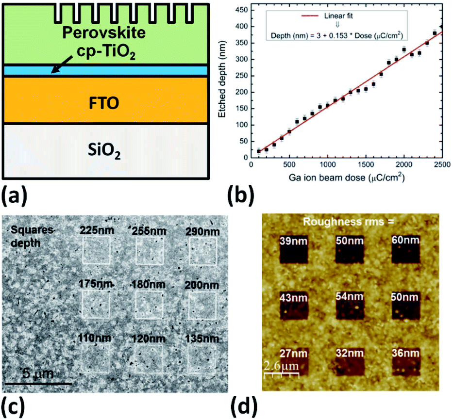 | ||
| Fig. 1 (a) Structure of the patterned perovskite thin film; (b) influence of the Ga ion dose on the etching depth; (c) SEM image of the perovskite surface with etched squared motifs of different depths. The depths are indicated on top of each square. (d) AFM image of the same zone as (c) with corresponding rms roughness values. | ||
FIB nano-fabrication process
The sample was introduced into the chamber of a focused ion beam system (Raith ionLINE), equipped with a Ga ion source. Milling was performed with a Ga + beam accelerated at 30 kV, an ion current of 44 pA, a fixed beam step size of 6 nm and 50 ion scans (loops) for each structure. To calibrate the milling rate of the perovskite film, squared motifs were created and characterized by atomic force microscopy (AFM). Fig. 1(b) shows the influence of the Ga ion dose on the etched depth. A linear relationship was measured, enabling the adjustment of the depth with the dose in future fabrication runs. The surface appearance and roughness created by the FIB milling on the perovskite film were observed by scanning electron microscopy (SEM) and AFM. As shown in the SEM image in Fig. 1(c), the perovskite surface looks identical between etched and un-etched zones, with alternative white and dark grains, as usually observed on this material.4 The rms roughness, measured by AFM, is indicated in Fig. 1(d) for the squares shown in Fig. 1(c), where the depth of each motif is also written on top. It varies between 27 nm and 60 nm and is of the same order of magnitude as the un-etched zones (around 30 nm).In this study, we chose to analyze arrays of one-dimensional (1D) structures made of grooves with a period, p, equal to 500 nm and 1 μm. Each array had a size of 50 × 50 μm2, in such a way that several patterns with different parameters could be fabricated on the same sample. Fig. 2(a) shows a SEM image of an array with a period equal to 500 nm, and a groove width (w) and depth (d) equal to 150 nm and 380 nm, respectively. Although some grains, which are probably residues from the erosion process, remain on the surface, the grooves are regularly spaced with abrupt edges confirming that the direct milling of a perovskite material with a FIB can be performed in a well-controlled and non-destructive manner.
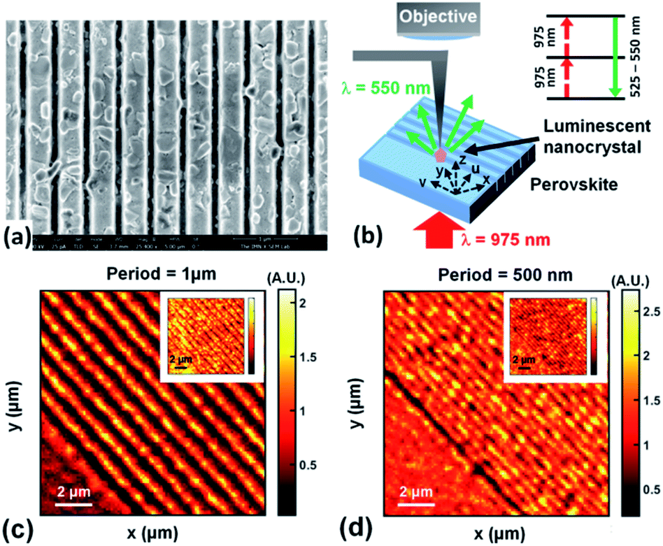 | ||
| Fig. 2 (a) SEM image of a 500 nm period grating with 150 nm wide grooves milled in the perovskite surface; (b) sketch of the experimental configuration for near-field measurements; (c) luminescence image obtained on a structure with p = 1 μm, d = 200 nm and w = 250 nm. Light polarization is parallel to the grooves; (d) same as (c) but with p = 500 nm. The insets show the corresponding AFM images simultaneously acquired during scanning (color scale: 0–300 nm). | ||
Near-field measurement technique
In order to measure the localization of the electromagnetic field and to evaluate the luminescence enhancement, we used a homemade scanning near-field optical microscope (SNOM) whose probe is a fluorescent nanocrystal. This nanocrystal is made of KY3F10 codoped with Er3+ (2 mole%) and Yb3+ (8 mole%) ions and is glued at the end of a sharp AFM tip.31,33 The nanocrystal synthesis is described in the ESI file.† The diameter of the nanocrystal used in this study is between 50 nm and 200 nm. The principle of the experiment is described in Fig. 2(b), which also contains the definition of the direction axis. The sample is set on a scanning stage and illuminated in a transmission mode with an internally modulated laser beam (λexc = 975 nm, fmod = 320 Hz, Ppeak = 30 mW) focused on a ∼50 μm wide spot. The tip scans the sample in the tapping mode and the nanocrystal is excited at λexc by the electromagnetic field localized on the surface. After the absorption of two photons, it emits light by luminescence in the 525–550 nm range. A simplified energy band diagram of the up-conversion excitation is shown in the inset of Fig. 2(b). A more detailed energy band diagram and a luminescence spectrum are shown in the ESI file.† The emitted light is collected with a large numerical aperture objective (N. A. = 0.8) and is sent to a photomultiplier tube connected to a lock-in amplifier. The images are recorded with a homemade Labview program that also drives the movement of the scanning stage.Simulation methods
A finite difference time domain (FDTD) method has been used to calculate the near-field intensity with a proprietary code Lumerical®, which provides us with a robust and reliable solver for Maxwell's equations. We use an impinging plane wave from the substrate side, of unit amplitude everywhere. In the simulation region we employ periodic boundary conditions using as unit cell with a span of 5 trenches in the plane (x and y directions) and perfect absorbing layers in the vertical (z-direction) that spans 10 μm. The refraction index of the perovskite material used was n = 2.32 at 975 nm wavelength as measured in ref. 46 by ellipsometry on a similar compound. The refractive indices for the rest of the involved materials are SiO2 = 1.45; FTO = 1.43, TiO2 = 2. Technical parameters are a mesh size of 5 nm in the xy-plane for the whole simulation; in z it is varied from 5 nm in the trenched area to 25 nm deep in the air and substrate. The pulse duration has been set to 1 ps, more than enough to ensure that all radiation has exited the simulation region. Under these conditions the total field is computed to give rise to the near field intensity color plots. All fields are normalized to the intensity of the impinging plane wave.C Results and discussion
Fig. 2(c) and (d) show two luminescence images obtained for structures having a period of 1 μm and 500 nm, respectively. The corresponding AFM images are shown in the insets (axes are defined in Fig. 2(b)). A portion of unstructured perovskite surface is visible on the lower left part of the images. The polarization of the incident laser beam was parallel to the grooves. As we can see, the presence of the grooves creates bright and dark lines, oriented in a direction parallel to the grooves. Although the measured quantity is the nanocrystal luminescence, we recently observed on other structures31,33 that it is directly linked to the intensity of the near-field on the surface at the excitation wavelength. The observed light contrast lines are due to the refractive index difference between the air and the perovskite (n = 2.32), which perturbs the incident plane wave and tends to confine the light in some particular zones. They result from the combination of the zero order diffraction and other modes in the perovskite layer that are evanescent in the vertical z-direction. These periodic structures constitute then a ridge waveguide grating directly engraved in the perovskite. Among the different geometrical parameters that influence the intensity of the electromagnetic field and luminescence, we decided to analyze in more detail the effect of the groove depth on the contrast.We therefore characterized three structures having the same period (p = 1 μm), the same groove width (w = 250 nm) and three groove depths (d = 100 nm, d = 150 nm, and d = 200 nm). The incident polarization was parallel to the grooves. The luminescence images are displayed in Fig. 3 and luminescence intensity cross-sections in the perpendicular direction to the grooves are shown in the insets. The oscillatory behavior is strong and presents highly contrasted fringes. If we compare the maximum intensity of the fringes Imax to the intensity on the unstructured surface Ib, we find that the ratio Imax/Ib increases from 2 to 3 when the groove depth increases from 100 nm to 200 nm [Fig. 3(d)]. Similarly, the contrast, defined as (Imax − Imin)/(Imax + Imin) where Imin is the minimum fringe intensity, also plotted in Fig. 3(d) as a function of the depth, augments from 0.45 to 0.65. So, both the intensity and contrast increase with the groove depth. To confirm the measured results, FDTD simulations, showing the variations of the near-field intensity with d, are depicted in Fig. 3(e). The maps are cuts in the plane perpendicular to the surface and the grooves (uz-plane). As we can see, the oscillatory behavior is very similar to the one observed in the experiments, and the contrast also increases as the depth increases (as it is confirmed by the increasing intensity of the bright lines appearing in the simulation plots). From the cross-sections, we see that the bright lines are located between the grooves whereas the minimum is located above them. This result can also be extracted from a careful comparison between luminescence and topographic experimental data, see Figs. 2(c and d), and it will be confirmed later (Fig. 4). In the simulation, two bright spots of less intensity are also visible on the sides of the grooves but they do not appear on the luminescence images, probably because of the lack of resolution of the fluorescent nanocrystal used in the measurements and also because they are mainly located inside the perovskite material. These experiments and the simulation indicate that the maximum luminescence enhancement takes place between the grooves.
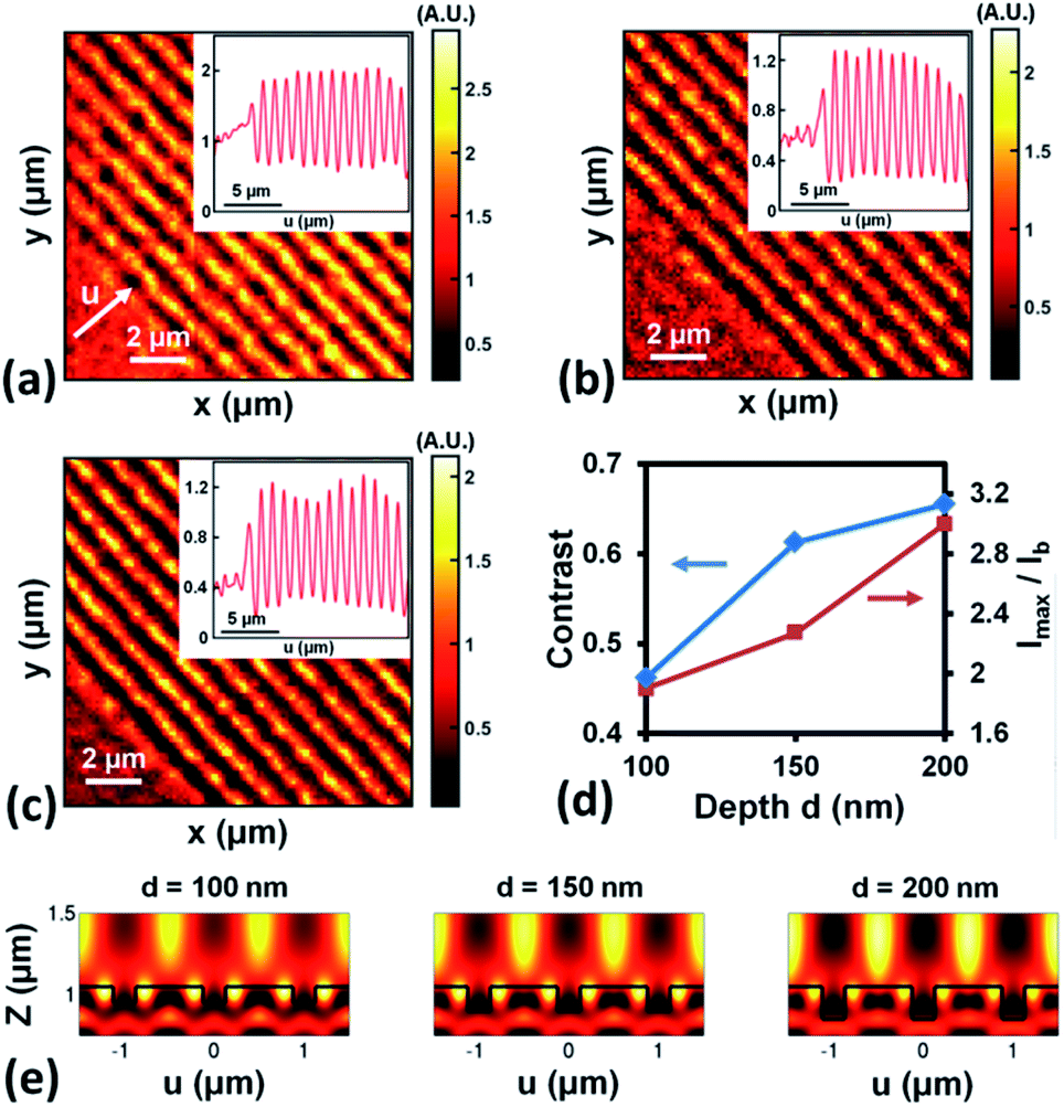 | ||
| Fig. 3 (a)–(c) Luminescence images (the polarization of the impinging wave is parallel to the grooves) measured by scanning the structures with p = 1 μm, w = 250 nm and d = 100 nm (a), d = 150 nm (b), and d = 200 nm (c). The insets show cross sections extracted from the images in a direction perpendicular to the grooves (u); (d) measured contrast and intensity ratio as a function of the depth; (e) FDTD calculations of the near-field intensity for the three structures. The maps are cuts in a plane perpendicular to the surface and to the grooves (uz-plane). Light polarization is again parallel to the grooves. | ||
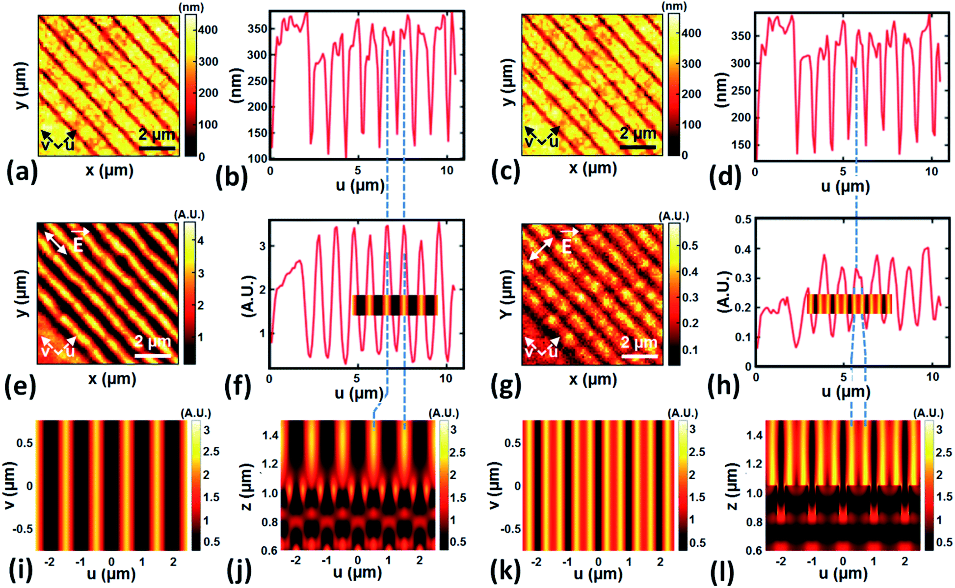 | ||
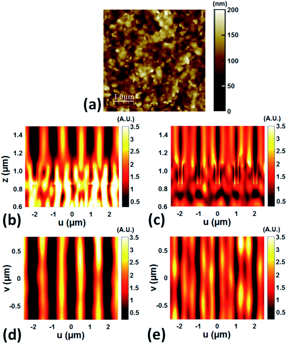
| Fig. 4 Topography (a–d) and luminescence (e–h) measured by scanning the array with period p = 1 μm and groove size w = 250 nm and d = 200 nm; (b, d, f and h) are cross-sections extracted from images (a, c, e and g). FDTD maps (i–l) of the electromagnetic near-field intensity calculated in the uv-plane parallel to the surface (i and k), and in the uz-plane perpendicular to both the surface and grooves (j and l) for the same array. The light polarization is either parallel (e, f, i and j) or perpendicular (g, h, k and l) to the grooves. | ||
All the previous images were measured with an illumination whose polarization was parallel to the grooves. We next studied the influence of the polarization direction on the luminescence enhancement. We focused on the sample with the larger contrast (p = 1 μm, w = 250 nm, and d = 200 nm) and compared the images obtained with both parallel and perpendicular polarizations [see Fig. 4(e) and (g)]. We cannot compare the relative intensities of the two images because the excitation intensity is different for each situation; however, it appears that the contrast is better in the case of the parallel polarization than for the perpendicular one. Moreover, the bright line is broader in the case of the perpendicular polarization. To understand this broadening, we calculated the near-field intensity by FDTD on this structure for both polarizations [see Fig. 4(i)–(l)]. In the case of the perpendicular polarization, the simulation reveals that the near-field is in fact composed of two peaks located on both sides of the grooves. These two peaks are not clearly contrasted, the intensity decreasing only by ∼30% between them [Fig. 4(k) and (l)]. In the experimental image, on the other hand, these two peaks are merged in a single one. The reasons that can explain this are (i) an eventual lack of resolution induced by the fluorescent nanocrystal glued at the tip end due to its size, and (ii) some roughness and residues that can enlarge the near-field distribution, thus impeding the separation and merging the two fringes. These two explanations are both credible and explain why we only see a single but broader peak. Moreover, by aligning and comparing the cross-sections taken along the direction perpendicular to the grooves (u-axis) in both experimental topography and luminescence images [Fig. 4(b), (d), (f) and (h)], as well as the FDTD maps, it can be seen that, independent of the polarization, the observed luminescence enhancement is located between the grooves. Considering the application we described in the introduction, i.e. the incorporation of fluorescent up-converting nanocrystals inside the nanostructured solar cell, illuminated by an unpolarized solar radiation, this experiment indicates that the nanocrystals have to be placed at this exact location, between the grooves.
From the luminescence maps shown in Fig. 2, 3, and 4, we see that the bright lines are not perfectly lined up and that they are not of constant intensity. This may be due to some residues left from the milling but also the roughness of the perovskite surface. Following this idea, we next tried to evaluate the effect of roughness on the near-field distribution on the surface. For that, we performed new FDTD calculations where we introduced some roughness in the perovskite surface using a built-in Lumerical® function for a random interface. We used a rms value of 40 nm and a correlation length of 200 nm, to resemble the grain size and height fluctuations observed experimentally (see AFM image in Fig. 5(a), where a nominal roughness of 30 nm was obtained, with grain sizes ranging between 50 and 400 nm). The results for an array of grooves with p = 1 μm, w = 250 nm and d = 200 nm are shown in Fig. 5(b and e), where intensity near-field maps taking into account the roughness are depicted along uz- and uv-planes for both light polarization directions. Compared to the FDTD maps without roughness shown for instance in Fig. 4(i)–(l), both the intensity and the shape are modified from fringe to fringe. The intensity can be locally enhanced and forms hot spots where luminescence is increased. In the case of the perpendicular polarization [Fig. 5(c) and (e)], we can see that the roughness tends to enlarge the fringes and merge them. Combined with the space-averaging due to the size of the fluorescent nanocrystal, it is not surprising that we were not able to separate the two fringes in the luminescence experiments [see Fig. 4(g) and (h)]. The effect of roughness is less important in the case of parallel polarization for which the fringes are more separated and contrasted [Fig. 5(b) and (d)]. As measured experimentally [see Fig. 4(f)], the full width at half maximum of the fringes for this polarization is approximately 400 nm, in agreement with the FDTD simulations shown in Fig. 4(i) and 5(d). This means that the luminescence enhancement, compared to the unstructured perovskite surface, occurs in this entire large zone. For our application, this situation is very interesting because this area is wide enough to be easily covered with a large number of fluorescent nanocrystals, thus contributing effectively to the improvement of the solar cell efficiency by increasing the absorption of infrared radiation and its re-emission in the visible range.
 | ||
| Fig. 5 AFM image of the topography of the perovskite surface (a); calculated FDTD maps of the near-field intensity for a groove array (p = 1 μm, w = 250 nm and d = 200 nm) incorporating roughness in the uz-plane for parallel (b) and perpendicular (c) incident light polarizations, and in the uv-plane for parallel (d) and perpendicular (e) polarizations. | ||
Another positive effect that both the nanostructuration and the presence of fluorescent nanocrystals could have is the improved scattering and trapping of visible light inside the perovskite layer. This could result in an enhanced absorption of the visible range of the solar spectra compared to the flat surface. We did not perform this study here, and remained focused on the near-field effects in the NIR, but it could be interesting to couple the effect of the nanostructuration in these two spectral zones (absorbed visible light and unabsorbed NIR) and optimize the structures to maximize both of them. On the other hand, many questions could be raised on the negative effects that could have the nanocrystals on the electrical properties of the solar cells. If we refer to recent studies, it has been reported that the incorporation of plasmonic20,21 or dielectric47 nanoparticles improved the PCE of the devices; thus we are therefore confident that fluorescent nanocrystals would have a very limited negative effect. Finally, in this study, we only varied the depth of the grooves, but a deeper optimization of their width as well as the period of the array could be carried out by FDTD and would probably contribute to designing structures that provide larger luminescence enhancements.
D Conclusions
We fabricated perovskite thin films used in hybrid solar cells and engraved their surface with a focused ion beam. Our aim was to create zones where infrared light is both localized and enhanced to boost the luminescence of up-converting nanocrystals placed on the material. We created arrays of grooves of variable depth and we studied them by near-field luminescence microscopy. We observed periodic luminescence variations and the formation of fringes oriented in the direction parallel to the grooves. A luminescence enhancement by a factor of 2 to 3 was measured when the nanocrystals are situated between the grooves compared to the unstructured perovskite surface. We found that the enhancement and the intensity contrast were both larger when increasing the groove depth. The polarization of the incident light also has an effect on the electromagnetic field distribution. Either a single fringe or two fringes appear when the incident polarization is parallel or perpendicular to the grooves, respectively. All the experimental results are in good agreement with numerical calculations performed by FDTD. The influence of the inhomogeneities of the perovskite layer was also studied and showed that the roughness tends to locally modify the intensity of the fringes and to distort their alignment. The measurements and simulations indicate that they can lead to additional hot spots. From our study, we showed that, for unpolarized radiation, which is the operating situation of solar cells under sunlight, the ideal position of the nanocrystals is between the grooves, where luminescence can be enhanced. As a prospect, further optimization could be made by changing the period and the width of the grooves and by improving the quality of the surface to reduce the roughness. The design of two-dimensional structures such as squares or circular disks could also lead to larger enhancements, and the structures would in that case be insensitive to polarization effects.Conflicts of interest
There are no conflicts to declare.Acknowledgements
The authors acknowledge the support from the DIM Nano-K program from “Région Ile de France”, from the Idex Paris Sciences & Lettres through the grant ANR-10-IDEX-0001-02 PSL, from the CNRS and the CSIC through the Spanish-French program PICS (grant SolarNano #PICS07687 and #PIC2016FR2), and the PROCES project (ANR-17-CEO5-0028-01). They also acknowledge the service from the MiNa Laboratory at IMN, which is funded by CM (project S2018/NMT-4291 TEC2SPACE), MINECO (project CSIC13-4E-1794) and EU (FEDER, FSE).References
- T. D. Lee and A. U. Ebong, Renewable Sustainable Energy Rev., 2017, 70, 1286 CrossRef CAS.
- M. Powalla, S. Paetel, E. Ahlswede, R. Wuerz, C. D. Wessendorf and T. Magorian Friedlmeier, Appl. Phys. Rev., 2018, 5, 041602 Search PubMed.
- M. Liu, M. B. Johnston and H. J. Snaith, Nature, 2013, 501, 395 CrossRef CAS PubMed.
- H. Zhou, Q. Chen, G. Li, S. Luo, T.-B. Song, H.-S. Duan, Z. Hong, J. You, Y. Liu and Y. Yang, Science, 2014, 345, 542 CrossRef CAS PubMed.
- J. H. Heo, S. H. Im, J. H. Noh, T. N. Mandal, C. S. Lim, J. A. Chang, Y. H. Lee, H. J. Kim, A. Sarkar, M. K. Nazeeruddin, M. Grätzel and S. Il Seok, Nat. Photonics, 2013, 7, 486 CrossRef CAS.
- W. S. Yang, J. H. Noh, N. J. Jeon, Y. C. Kim, S. Ryu, J. Seo and S. Il Seok, Science, 2015, 348, 1234 CrossRef CAS PubMed.
- Q. Jiang, L. Zhang, H. Wang, X. Yang, J. Meng, H. Liu, Z. Yin, J. Wu, X. Zhang and J. You, Nat. Energy, 2017, 2, 16177 CrossRef CAS.
- W. S. Yang, B.-W. Park, E. H. Jung, N. J. Jeon, Y. C. Kim, D. U. Lee, S. S. Shin, J. Seo, E. K. Kim, J. H. Noh and S. I. Seok, Science, 2017, 356, 1376 CrossRef CAS PubMed.
- P. Bermel, C. Luo, L. Zeng, L. C. Kimerling and J. D. Joannopoulos, Opt. Express, 2007, 15, 16986 CrossRef CAS PubMed.
- S. B. Mallick, M. Agrawal and P. Peumans, Opt. Express, 2010, 18, 5691 CrossRef CAS PubMed.
- Y. Yu, V. E. Ferry, P. Alivisatos and L. Cao, Nano Lett., 2012, 127, 3674 CrossRef PubMed.
- D.-L. Wang, H.-J. Cui, G.-J. Hou, Z.-G. Zhu, Q.-B. Yan and G. Su, Sci. Rep., 2016, 6, 18922 CrossRef CAS PubMed.
- A. Peer, R. Biswas, J.-M. Park, R. Shinar and J. Shinar, Opt. Express, 2017, 25, 10704 CrossRef CAS PubMed.
- L. Zheng, Y. Ma, S. Chu, S. Wang, B. Qu, L. Xiao, Z. Chen, Q. Gong, Z. Wu and X. Hou, Nanoscale, 2014, 6, 8171 RSC.
- A. R. Pascoe, S. Meyer, W. Huang, W. Li, I. Benesperi, N. W. Duffy, L. Spiccia, U. Bach and Y.-B. Cheng, Adv. Funct. Mater., 2016, 26, 1278 CrossRef CAS.
- M. Jošt, S. Albrecht, L. Kegelmann, C. M. Wolff, F. Lang, B. Lipovšek, J. Krč, L. Korte, D. Neher, B. Rech and M. Topič, ACS Photonics, 2017, 4, 1232 CrossRef.
- Z. Hu, J. García-Martín, Y. Li, L. Billot, B. Sun, F. Fresno, A. García-Martín, M. U. González, L. Aigouy and Z. Chen, ACS Appl. Mater. Interfaces, 2020, 12, 5979 CrossRef CAS PubMed.
- M. E. Ferry, L. A. Sweatlock, D. Pacifici and H. A. Atwater, Nano Lett., 2008, 8, 4391 CrossRef PubMed.
- H. A. Atwater and A. Polman, Nat. Mater., 2010, 9, 205 CrossRef CAS PubMed.
- R. T. Ginting, S. Kaur, D.-K. Lim, J.-M. Kim, J. H. Lee, S. H. Lee and J.-W. Kang, ACS Appl. Mater. Interfaces, 2017, 9, 36111 CrossRef CAS PubMed.
- Q. Luo, C. Zhang, X. Deng, H. Zhu, Z. Li, Z. Wang, X. Chen and S. Huang, ACS Appl. Mater. Interfaces, 2017, 9, 34821 CrossRef CAS PubMed.
- D. M. Wu, A. Garcia-Etxarri, A. Salleo and J. A. Dionne, J. Phys. Chem. Lett., 2014, 5, 4020 CrossRef CAS PubMed.
- P. Wang, Z. Li, W. J. Salcedo, Z. Sun, S. Huang and A. G. Brolo, Phys. Chem. Chem. Phys., 2015, 17, 16170 RSC.
- M. Schoenauer Sebag, Z. Hu, K. de Oliveira Lima, H. Xiang, P. Gredin, M. Mortier, L. Billot, L. Aigouy and Z. Chen, ACS Appl. Energy Mater, 2018, 18, 3537 CrossRef.
- Y.-L. Wang, N. M. Estakhri, A. Johnson, H.-Y. Li, L.-X. Xu, Z. Zhang, A. Alù, Q.-Q. Wang and C.-K. Shih, Sci. Rep., 2015, 5, 10196 CrossRef CAS PubMed.
- J.-C. Boyer and F. C. J. M. Van Veggel, Nanoscale, 2010, 2, 1417 RSC.
- J. He, W. Zheng, F. Ligmajer, C.-F. Chan, Z. Bao, K.-L. Wong, X. Chen, J. Hao, J. Dai, S.-F. Yu and D. Y. Lei, Renewable Sustainable Energy Rev., 2017, 6, 16217 Search PubMed.
- D. Zhou, D. Liu, W. Xu, Z. Yin, X. Chen, P. Zhou, S. Cui, Z. Chen and H. Song, ACS Nano, 2016, 10, 5169 CrossRef CAS PubMed.
- Z. Yin, H. Li, W. Xu, S. Cui, D. Zhou, X. Chen, Y. Zhu, G. Qin and H. Song, Adv. Mater., 2016, 28, 2518 CrossRef CAS PubMed.
- S. Han, R. Deng, X. Xie and X. Liu, Angew. Chem., Int. Ed., 2014, 53, 11702 CrossRef CAS PubMed.
- H.-J. Lin, K. de Oliveira Lima, P. Gredin, M. Mortier, L. Billot, Z. Chen and L. Aigouy, Appl. Phys. Lett., 2017, 111, 251109 CrossRef.
- J. C. Goldschmidt and S. Fischer, Adv. Opt. Mater., 2015, 3, 510 CrossRef CAS.
- L. Aigouy, M.-U. González, H.-J. Lin, M. Schoenauer-Sebag, L. Billot, P. Gredin, M. Mortier, Z. Chen and A. García-Martín, Nanoscale, 2019, 11, 10365 RSC.
- P. Anger, P. Bharadwaj and L. Novotny, Phys. Rev. Lett., 2006, 96, 113003 CrossRef PubMed.
- S. Kühn, U. Håkanson, L. Rogobete and V. Sandoghdar, Phys. Rev. Lett., 2006, 97, 017402 CrossRef PubMed.
- S. Fischer, D. Kumar, F. Hallermann, G. V. Plessen and J. C. Goldschmidt, Opt Express, 2016, 24, 460 CrossRef PubMed.
- P. Albella, M. A. Poyli, M. K. Schmidt, S. A. Maier, F. Moreno, J. J. Saenz and J. Aizpurua, J. Phys. Chem. C, 2013, 117, 13573 CrossRef CAS.
- B. Jeong, H. Han and C. Park, Adv. Mater., 2020, 32, 2000597 CrossRef CAS PubMed.
- J. Harwell, J. Burch, A. Fikouras, M. C. Gather, A. Di Falco and I. D. W. Samuel, ACS Nano, 2019, 13, 3823 CrossRef CAS PubMed.
- M. S. Alias, Y. Yang, T. K. Ng, I. Dursun, D. Shi, M. I. Saidaminov, D. Priante, O. M. Bakr and B. S. Ooi, J. Phys. Chem. Lett., 2016, 7, 137 CrossRef CAS PubMed.
- Y. Wang, Z. Gu, Y. Ren, Z. Wang, B. Yao, Z. Dong, G. Adamo, H. Zeng and H. Sun, ACS Appl. Mater. Interfaces, 2019, 11, 15756 CrossRef CAS PubMed.
- K. Wang, G. Xing, Q. Song and S. Xiao, Adv. Mater., 2021, 33, 2000306 CrossRef CAS PubMed.
- A. Kessel, C. Frydendahl, S. R. K. C. Indukuri, N. Mazurski, P. Arora and U. Levy, Adv. Opt. Mater., 2020, 8, 2001627 CrossRef CAS.
- E. Edri, S. Kirmayer, D. Cahen and G. Hodes, J. Phys. Chem. Lett., 2013, 4, 897 CrossRef CAS PubMed.
- M. Saliba, T. Matsui, J.-Y. Seo, K. Domanski, J.-P. Correa-Baena, M. Khaja Nazeeruddin, S. M. Zakeeruddin, W. Tress, A. Abate, A. Hagfeldtd and M. Grätzel, Energy Environ. Sci., 2016, 9, 1989 RSC.
- L. J. Phillips, A. M. Rashed, R. E. Treharne, J. Kay, P. Yates, I. Z. Mitrovic, A. Weerakkody, S. Hall and K. Durose, Sol. Energy Mater. Sol. Cell., 2016, 147, 327 CrossRef CAS.
- C. Zhang, Z. Li, X. Deng, B. Yan, Z. Wang, X. Chen, Z. Sun and S. Huang, Sol. Energy, 2019, 188, 839 CrossRef CAS.
Footnote |
| † Electronic supplementary information (ESI) available: The nanocrystal fabrication procedure, characterization, and near-field tip fabrication procedure have been described in the ESI data file. See DOI: 10.1039/d1na00782c |
| This journal is © The Royal Society of Chemistry 2022 |