
 Open Access Article
 This Open Access Article is licensed under a Creative Commons Attribution-Non Commercial 3.0 Unported Licence
Cross-sectional shape evolution of GaN nanowires during molecular beam epitaxy growth on Si(111)†
Roman
Volkov
 a,
Nikolai I.
Borgardt
a,
Oleg V.
Konovalov
b,
Sergio
Fernández-Garrido‡
c,
Oliver
Brandt
c and
Vladimir M.
Kaganer
*c
a,
Nikolai I.
Borgardt
a,
Oleg V.
Konovalov
b,
Sergio
Fernández-Garrido‡
c,
Oliver
Brandt
c and
Vladimir M.
Kaganer
*c
aNational Research University of Electronic Technology — MIET, Bld. 1, Shokin Square, Zelenograd, Moscow 124498, Russia
bESRF – The European Synchrotron, 71 avenue des Martyrs, 38043 Grenoble, France
cPaul-Drude-Institut für Festkörperelektronik, Leibniz-Institut im Forschungsverbund Berlin e. V., Hausvogteiplatz 5–7, 10117 Berlin, Germany. E-mail: kaganer@pdi-berlin.de
First published on 3rd December 2021
Abstract
We study the cross-sectional shape of GaN nanowires (NWs) by transmission electron microscopy. The shape is examined at different heights of long NWs, as well as at the same height for NWs of different lengths. Two distinct trends in the evolution of the cross-sectional shape along the NW length are observed. At the top, merging NWs develop common {1![[1 with combining macron]](https://www.rsc.org/images/entities/char_0031_0304.gif) 00} side facets. At the bottom, the NWs acquire roundish shapes. This observation is explained by the entirely different NW environments at the top and the bottom of the NWs. At the top, NWs are exposed to the Ga and N atomic fluxes giving rise to axial growth, resulting in the equilibrium growth shape with zero growth rate at the {100} facets. At the bottom, NWs are shadowed from the impinging fluxes and are only annealed, allowing them to eventually approach the equilibrium crystal shape. The study of identical samples by grazing incidence small-angle X-ray scattering independently confirms these trends in the shape evolution of the sidewall facets.
00} side facets. At the bottom, the NWs acquire roundish shapes. This observation is explained by the entirely different NW environments at the top and the bottom of the NWs. At the top, NWs are exposed to the Ga and N atomic fluxes giving rise to axial growth, resulting in the equilibrium growth shape with zero growth rate at the {100} facets. At the bottom, NWs are shadowed from the impinging fluxes and are only annealed, allowing them to eventually approach the equilibrium crystal shape. The study of identical samples by grazing incidence small-angle X-ray scattering independently confirms these trends in the shape evolution of the sidewall facets.
1 Introduction
GaN nanowires (NWs) are currently considered as potential candidates for future nanoscale device applications.1 The main attraction of these structures lies in the fact that threading dislocations, which intersect epitaxial GaN layers in high densities, are entirely absent in thin GaN NWs regardless of the substrate. This fact is due to the close vicinity of the free NW sidewall surface, making it energetically favorable for dislocations to bend and leave the crystal at the sidewalls instead of remaining in the NW.2,3 This beneficial effect is not the only consequence of the exceptionally high surface-to-volume ratio of GaN NWs. Rather, several properties of NWs important for applications are affected or governed by the close vicinity of the sidewall surface, sometimes with undesirable (electrical depletion,4 nonradiative recombination5) and sometimes with beneficial consequences (elastic strain relief,6 high sub-bandgap absorption7).A number of applications of GaN NWs even exclusively relies on surface effects, such as gas sensing,8 solar water-splitting,9 and CO2 reduction.10,11 Most of these effects do not only require the mere presence of a surface, but depend sensitively on the crystallographic nature and termination of this surface. The sidewalls facet orientation is also particularly important for the future development of hybrid inorganic/organic semiconductor devices, since the electronic properties of hybrid interfaces vary depending on the facet.12 Furthermore, from an epitaxial point of view, the actual orientation of the NW facets is critical during the fabrication of devices with a core–shell geometry because, besides affecting the formation of native point defects, both the relative incorporation ratio of group-III elements and the dopants incorporation efficiencies depend on the crystal orientation.13–16 It is thus imperative to understand which planes form the sidewall facets of GaN NWs and how they are affected by growth and environmental conditions.
GaN NWs form spontaneously on various substrates in molecular beam epitaxy (MBE) at high substrate temperature and effectively N rich conditions.17,18 The most common substrate for GaN NWs in MBE is Si(111). On this substrate, GaN NWs form high-density ensembles, regardless of nucleation and growth conditions. The fraction of the substrate surface covered by NWs is at least 20%. The high density of NWs gives rise to their coalescence by bundling: adjacent NWs attract each other, merge together and grow further in height as a single NW aggregate. The driving force of bundling is the reduction of the surface energy of the merging facets on the expense of the bending energy.19 The coalesced aggregates often exhibit irregular cross-sectional shapes,20 but the facets observed in top-view micrographs obtained by scanning electron microscopy (SEM) are formed by GaN{100} planes.20–22 High-resolution transmission electron microscopy (TEM) confirmed this observation, but revealed that the vertices formed by adjacent {100} facets are not atomically abrupt, but rounded.20 On the other hand, numerous ab initio calculations23–31 have shown that the surface energies of {100} and {11![[2 with combining macron]](https://www.rsc.org/images/entities/char_0032_0304.gif) 0} facets are close to each other, so that these two facets would be expected to be present with comparable areas in the equilibrium crystal shape.
0} facets are close to each other, so that these two facets would be expected to be present with comparable areas in the equilibrium crystal shape.
The aim of the present study is to clarify this apparent contradiction between experiment and theory by examining the cross-sectional shapes of NWs at different stages of their growth. To this end, we study the evolution of the cross-sectional sizes and shapes of NWs in the process of MBE growth. We compare TEM micrographs of plan-view cross sections cut out at different heights from one and the same sample with 2.4 μm long GaN NWs and the micrographs of samples with NWs of different lengths cut out at the same height. The results of this TEM investigation are also compared with the cross-sectional size and shape distributions obtained from grazing incidence small-angle X-ray scattering (GISAXS) experiment. We observe two distinct cross-sectional shapes depending on both the NW length and the height of the cross section. At their very top, NWs develop common {100} side facets of merging NWs. At the bottom, NWs attain roundish shapes formed by both {100} and stepped {110} planes. The origin of this difference is discussed.
2 Experimental
2.1 Nanowire growth
For the present study, we have selected three samples with NWs of lengths 230, 650, and 2430 nm from series A studied in ref. 19. The sample with the longest NWs has been used to prepare cuts at different heights for the TEM study, while the two other samples were used to make cuts at about the same height of 200 nm for a comparison.The GaN NWs were synthesized in a molecular beam epitaxy system equipped with a solid-source effusion cell for Ga and a radio-frequency N2 plasma source for generating active N. The samples were grown on Si(111) substrates, which were preliminarily etched in diluted HF (5%), outgassed above 900 °C for 30 min to remove any residual SixOy from the surface, and exposed to the N plasma for 10 min. The substrate growth temperature was approximately 800 °C, as measured with an optical pyrometer. The Ga and N fluxes, calibrated by determining the thickness of GaN films grown under N- and Ga-rich conditions,32 were 0.3 and 0.75 monolayers per second, respectively, where one monolayer corresponds to an areal site density of 1.14 × 1015 cm−2. The growth time is the only parameter that was varied among the samples to obtain ensembles of NWs with different lengths.
2.2 TEM sample preparation
TEM plan-view specimens parallel to the Si(111) substrate surface were prepared using a FEI Helios NanoLab 650 DualBeam workstation equipped with a Kleindick MM3A-EM micromanipulator and a gas injection system allowing the local deposition of a mix of platinum and amorphous carbon. The in situ lift-out technique33 was used. First, for the sake of mechanical stabilization, the space between NWs was filled with a platinum and amorphous carbon mix, using electron beam induced deposition. This mix was used instead of commonly employed epoxy glue, which becomes rather flexible under electron or ion irradiation and causes an undesirable specimen bending.At the beginning of the fastening process, we scanned the substrate region near its cleavage edge by the electron beam with a relatively small current and a dwell time of 0.1 nA and 50 ns, respectively. Such low-irradiation conditions were employed to cover NWs by a thin conductive layer preventing substantial coalescence of NWs due to their charging. After about 5 min, the current and dwell time were increased to 1.6 nA and 1 μs, respectively, to speed up the deposition process. The acceleration voltage was 30 kV instead of the common value of 2 kV to guarantee a uniform deposition along the full length of NWs. These parameters were found empirically as a result of several trials to avoid possible coalescence of the NWs during the TEM specimen preparation.
After fastening the NWs together and protecting them from ion beam damage by an additional platinum layer of about 1 μm in thickness, we created a rectangular trench underneath by focused ion beam milling of the cleavage side. Then, a formed block containing GaN NWs was cut off from the substrate, transferred using a micromanipulator, and attached to a TEM grid by Pt deposition.
The sample with 2430 nm long NWs was used to prepare TEM foils at distances of approximately 200, 800, 1500, and 2300 nm from the substrate surface, as illustrated in Fig. 1. The preparation requires the control of the milling process by preliminarily creating a stream file with a table of ion beam stopping positions and dwell times to form the specimen with such complex stair-step shape, as described in detail in ref. 34. Two other samples with shorter NWs were sectioned at a distance of about 200 nm from the substrate. They were thinned using a standard rectangular milling pattern providing a single flat surface. The accelerating voltage for the ions was 30 keV during this process. The four-section specimen was about 20 × 8 μm2 in size, while the other specimens measured about 10 × 6 μm2.
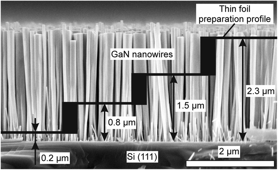 | ||
| Fig. 1 SEM micrograph of a GaN NW ensemble on Si(111) with a scheme of the stair-step thin foil prepared from the sample. The lateral length of the steps is 4–5 μm and is thus not to scale in the figure. | ||
After the specimen thicknesses reached about 100–150 nm, we carried out their final thinning using a Gatan PIPS 691 instrument with a broad beam of Ar ions with an energy of 2 keV. The milling progress was controlled by periodically stopping it and observing the foils in the transmission electron microscope. This step ensured the elimination of the amorphized and contaminated surface layer and also allowed us to avoid the curtain effect often appearing during focused ion beam thinning. The thickness of the prepared specimens was estimated by the convergent-beam electron diffraction technique of TEM to be about 20–40 nm.
2.3 TEM study
The prepared specimens were studied using a FEI Titan Themis 200 transmission electron microscope equipped with an X-FEG electron source, a spherical aberration corrector for an image-forming system, a high-angle annular dark-field (HAADF) detector of electrons, and a Ceta 16M camera. The investigation was performed at the acceleration voltage of 200 kV. Spatial resolutions in high-resolution transmission and scanning transmission electron microscopy (HRTEM and HRSTEM) modes are 0.9 and 1.6 Å, respectively.Images of NWs with a relatively low magnification, without visualizing the atomic structure, were obtained in STEM mode.35 In this mode, contrast originating from strain and crystalline defects is eliminated to a large extent, allowing us to clearly distinguish the GaN NWs from the surrounding material, and to digitally analyze their shape.
HRTEM was used as the most reliable technique to directly visualize the atomic structure of the crystal lattice. We always recorded HRTEM micrographs both without and with the objective aperture (letting only the first-order diffraction reflections pass), which simplifies the recognition of defects and interfaces. HRTEM micrographs were acquired close to the Gaussian focus position of the objective lens, where 2nd and 3rd aberrations were minimized.
Electron microdiffraction patterns were obtained from specimen regions of several micrometers in diameter, to reveal variations in the range of NW orientations at different distances from the substrate. Preliminarily, we set to zero currents through hexapoles of the image aberration corrector, because their operation produces large distortions of diffraction patterns. The diffraction patterns were corrected before the analysis for residual elliptical distortion using the ring diffraction pattern of a standard specimen of polycrystalline NiOx.
Quantitative analysis of the NW shapes requires conversion of the STEM images to binary format, where black areas against a white background correspond to individual NWs. We performed this procedure using the “Magic Wand” tool of the Fiji open source image processing package36 to select cross-sections of individual NWs one by one. Some manual correction was needed to differentiate closely located objects. Details of the image processing and the NW size determination are presented in the ESI.†
2.4 Grazing incidence small-angle X-ray scattering (GISAXS)
Two samples identical to the ones chosen for the TEM study, with NW lengths of 230 and 650 nm, have been already studied by GISAXS.37 In the present paper, we extend the analysis of the cross-sectional shapes of NWs based on these data.The GISAXS measurements were performed at the beamline ID10 of the European Synchrotron Radiation Facility (ESRF) using an X-ray energy of 22 keV (wavelength 0.5636 Å). The incident beam was directed at a grazing incidence to the substrate. The chosen grazing incidence angle was 0.2°, i.e., about 2.5 times larger than the critical angle of the substrate, to avoid possible complications of the scattering pattern typical for grazing incidence X-ray scattering.38 A two-dimensional detector (Pilatus 300K, Dectris) placed at a distance of 2.38 m from the sample provided a resolution of 8.06 × 10⁻³ nm−1.
The processing of the measured two-dimensional intensity distribution is described in ref. 37. In brief, small-angle scattering around the transmitted beam is used. Each qz-scan through the intensity map  (where x axis is parallel to the surface and z axis normal to it) is fitted to a Gaussian, and its maximum value is taken to be the GISAXS intensity I(qx). The widths of the Gaussians Δqz are found to linearly depend on qx, which is due to a random tilt of the long axes of NWs with respect to the substrate surface normal. The full width at half maximum (FWHM) of the tilt is found to be 5.9° and 5.1° for the two samples.
3 Results
Fig. 2 presents top-view HAADF STEM images acquired from regions located at different distances from the substrate, as schematized in Fig. 1. The NWs are recognized as compact regions with almost homogeneous or monotonically varying intensity. They are either brighter or darker, depending on their tilt, than the surrounding material (platinum nanoparticles and amorphous carbon deposited during TEM specimen preparation). In the surrounding material, the contours observed around the NWs are a consequence of the variation of the platinum-to-carbon ratio during their deposition, caused by changes of the electron beam current, and the joining of layers forming around neighboring NWs. Black regions in Fig. 2 are residual voids, which are mainly present at the bottom of the NW ensemble close to the interface with the substrate, and reflect the incomplete penetration of the platinum–carbon mix from the top to the bottom of the sample.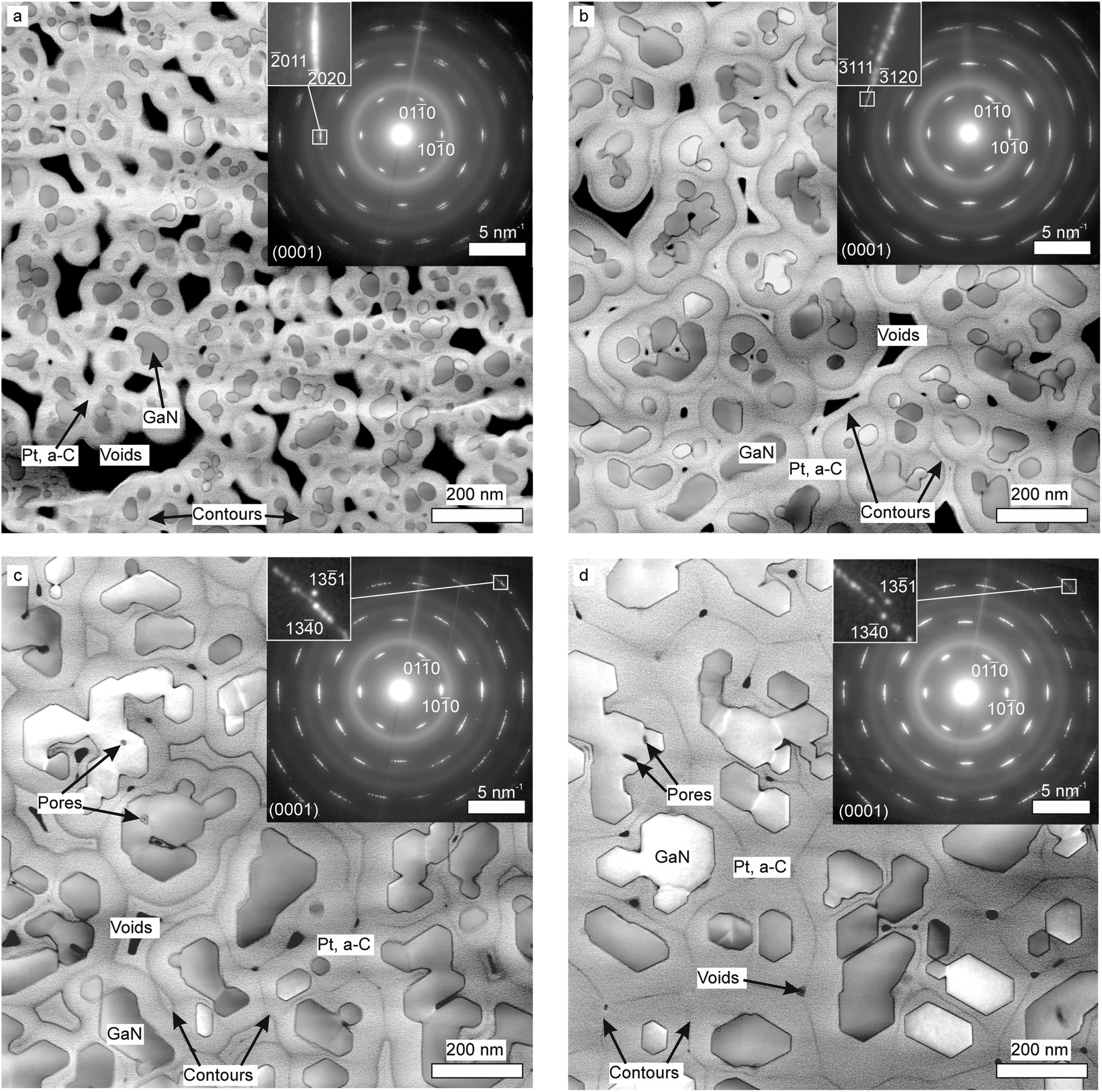 | ||
| Fig. 2 HAADF STEM micrographs and electron microdiffraction patterns (insets) of cross-sections at distances of about (a) 200, (b) 800, (c) 1500, and (d) 2300 nm from the substrate. | ||
The electron microdiffraction patterns shown in the insets of Fig. 2 reveal reflection arcs instead of spots indicating an axial misorientation (twist) of individual NWs. Additional reflections resulting from tilted NWs are also observed. Some of them are indexed in the magnified images of the individual arcs. From the bottom (Fig. 2a) to the top (Fig. 2d) of the NW ensemble, the number and intensity of these reflections decreases, revealing a reduction of the NW tilt. The reduction of tilt from the bottom to the top of the NWs is also directly seen in Fig. 1.
Transformation of the sizes and shapes of NWs is evident from Fig. 2a–d. At the bottom (Fig. 2a), NWs are small and roundish in their cross-sections. At the top (Fig. 2d), the NW sides are notably larger and mostly bounded with {100} facets. Some of the NW cross sections are hexagons, while others are large irregular aggregates formed by the coalescence of individual NWs. Fig. 2b and c show that this transformation proceeds continuously with increasing distance from the substrate. Some NWs in Fig. 2c and d contain pores. Careful examination of the images showed that pores are absent in the bottom parts of NWs, and the number of them increases with the height over the substrate.
A quantitative statistical analysis of the cross-sectional areas of individual NWs has been performed on a series of images similar to the ones presented in Fig. 2. In total, 2578, 1494, 561, and 419 NWs were analyzed at distances of 200, 800, 1500, and 2300 nm from the substrate, respectively. These numbers are large enough to ensure small errors in the statistical analysis.
The NW densities at the respective distances from the substrate are presented in Fig. 3a by solid squares. For a comparison, we reproduce by open circles the results of the analysis of a series of samples19 grown at the same conditions as the sample analyzed by TEM in the present work. The only parameter varying in the series was the growth time and hence the NW length. The analysis was performed using top-view SEM micrographs. The data point for the longest NWs has not been presented in ref. 19.
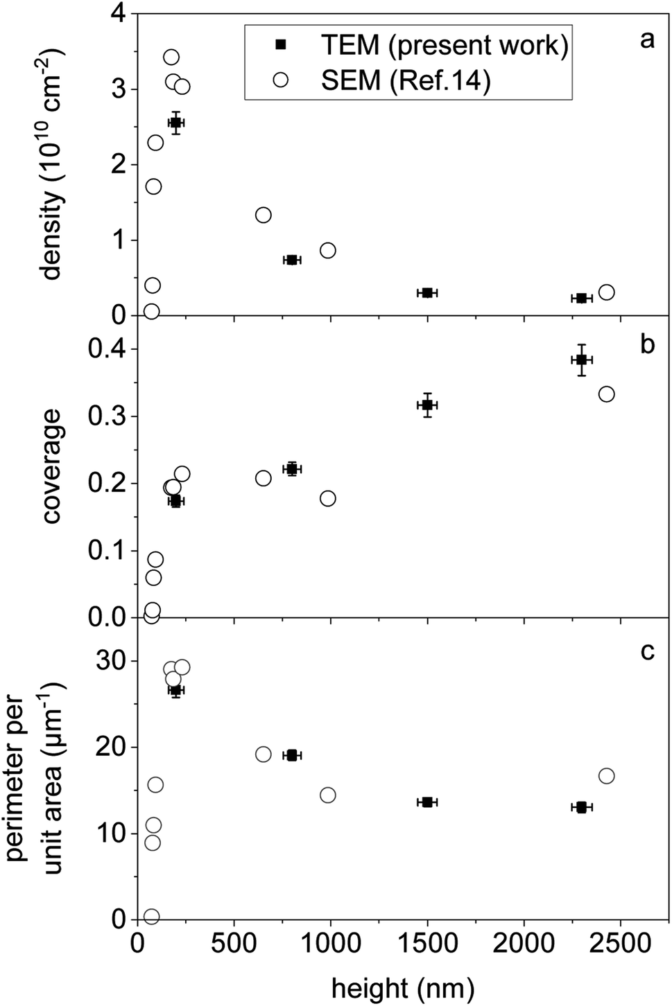 | ||
| Fig. 3 (a) Density, (b) coverage (fraction of surface area covered by NWs), and (c) total perimeter of NWs per unit surface area as a function of height (distance from the substrate). Solid squares present the data obtained from the statistical analysis of TEM images of the sections at different heights from a single sample performed in the present work. Open circles are the result of the analysis of top-view SEM micrographs on a series of samples performed in ref. 19. The series of samples in ref. 19 and the sample studied in the present work are grown under identical conditions. The data point for the longest NWs and the perimeters in (c) have not been presented in ref. 19. | ||
The error bars in Fig. 3 are estimated as follows. The determination of the distances from the substrate (abscissa of Fig. 3) is affected by a possible misalignment of the horizontal scanning direction of the focused ion beam with respect to the substrate orientation by up to 0.1°. The uncertainty of the substrate position is given by the distance of about 10 nm between subsequent slices formed by the focused ion beam. The errors in the ordinates in Fig. 3 originate from (i) the magnification calibration error of the microscope of less than 1%, (ii) NWs at the image edges which can be either included or excluded from the analysis, and (iii) segmentation errors when proceeding from the original to binary (black and white) images. The latter quantity was estimated by comparing 10 independent procedures applied to small regions of the images.
Fig. 3a shows that the evolution of the NW density with the distance from the substrate in a single sample is in good agreement with the densities at the NW top in a series of samples grown for different times. Nucleation of NWs proceeds until the average NW length reaches 200 nm, and gives rise to a NW density of about 3 × 1010 cm−2. During further NW growth, their density decreases by an order of magnitude as their length reaches 1000 nm, and remains almost constant during the subsequent NW elongation.
Fig. 3b presents the evolution of the fraction of the substrate area covered by NWs (coverage). We again compare TEM measurements at different heights in a single sample in the present work (solid squares) with the analysis of the top-view SEM micrographs of a series of samples grown under the same conditions for different times19 (open circles). The results are in good agreement and show that the coverage quickly increases to 0.2 during the nucleation stage and then slowly increases to 0.4 as the NWs grow in length to 2.4 μm.
Fig. 3c shows the evolution of the total perimeter of NWs per unit surface area. The TEM data obtained at different heights of a single sample and the SEM data from a series of samples are represented by solid squares and open circles, respectively, in the same way as above. The perimeters of individual NWs were measured and used in ref. 19 to obtain the NW circularity, but were not presented directly. A comparison of the plots in Fig. 3b and c reveals a peculiar development of the NW ensemble: after nucleation has ceased at a NW length of about 200 nm, the total NW area (coverage) increases while the total perimeter decreases. This finding implies a transformation of the cross-sectional shapes of NWs. We will discuss this phenomenon, as well as other consequences that follow from the comparison of the plots in Fig. 3, in Section 4.
Fig. 4 presents distributions of NW radii at different heights obtained by a statistical analysis of the TEM micrographs similar to the ones in Fig. 2. The NW radii R are obtained from their cross-sectional areas A and perimeters P as R = 2A/P. The NW radius defined this way is more suitable than the equivalent-disk approximation  when comparing NWs with regular and irregular cross sections, and has been used previously to describe the surface recombination rate of excitons for NWs of arbitrary shape.39 The lines in Fig. 4a are the respective distributions obtained by the Monte Carlo simulation of the GISAXS intensity described below. We note that the GISAXS intensity is collected from the whole NW volume.
 | ||
| Fig. 4 Histograms of the NW radii obtained from the statistical analysis of TEM micrographs of the sections of the 2.4 μm long NWs at a height of (a) 200 nm, (b) 800 mn, (c) 1500 nm, and (d) 2300 nm. The NW radii are defined as R = 2A/P, where A is the NW cross-sectional area and P its perimeter. The curves in (a and b) are obtained by Monte Carlo simulation of the GISAXS intensity for the samples with NW lengths of 230 and 650 nm. | ||
As we have already noticed above, the shape of the NW cross sections in Fig. 2 continuously evolves from roundish at the distance of 200 nm from the substrate to faceted at the distance of 2300 nm. For a comparison, Fig. 5 presents cross sections of three samples with NWs of different lengths, taken at the same height of about 200 nm. The cross-sectional shape at the bottom parts of NWs, which originally were hexagonal for short NWs (Fig. 5a), becomes roundish during further NW growth (Fig. 5c).
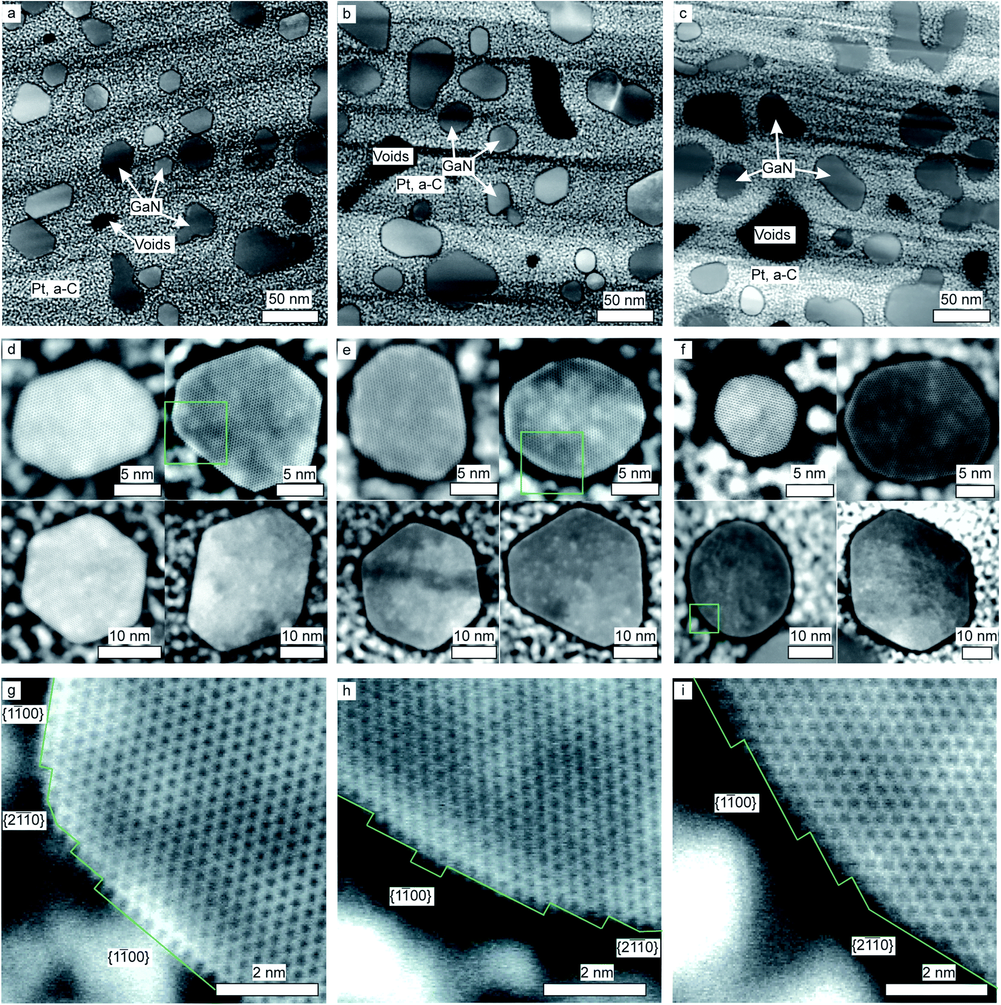 | ||
| Fig. 5 HAADF STEM micrographs of GaN NWs (a, d and g) 230, (b, e and h) 650, and (c, f and i) 2400 nm in length. The cross sections are taken at the same distance of about 200 nm from the substrate. The squares in (d–f) highlight the parts of the NWs presented in (g–i) with a higher magnification. | ||
Fig. 5d–f present magnified cross-sectional micrographs of a few exemplary NWs. The cross sections of short NWs in Fig. 5d have hexagonal shape, which evolves to a roundish one for long NWs in Fig. 5f. This shape transformation is the same for both the thinnest and thicker NWs in the top and the bottom rows of Fig. 5d–f, respectively. The high-resolution micrographs in Fig. 5g–i reveal the atomic structure of the side NW surfaces. Short NWs exhibit {100} facets that are almost atomically perfect and flat, while longer NWs possess in addition {110} facets as well as a large number of atomic steps, which makes their shape appear roundish in lower magnification.
Further insight into the cross-sectional shape transformation can be obtained from HRTEM micrographs of coalesced NWs. Fig. 6 shows an example of an irregularly shaped NW aggregate formed by the coalescence of three NWs, prepared at a distance of 200 nm from the substrate. The difference in their contrast is caused by a small relative misorientation of the individual NWs: the top and the bottom NWs in Fig. 6 are rotated about the vertical axis (twisted) with respect to the middle one by 0.6° and 0.7°, respectively. The dashed lines in Fig. 6 follow the {100} facets of the initial uncoalesced NWs. Dotted lines mark the present NW boundaries, recognized by the rapid change of the image intensity. The boundary between two large NWs is rotated with respect to the initial boundary by 20°. An inspection of a large number of coalesced NWs in TEM micrographs with a lower magnification shows that the rotation of the boundary between the NWs is a common effect and the orientations of the rotated boundaries are close to the {110} planes.
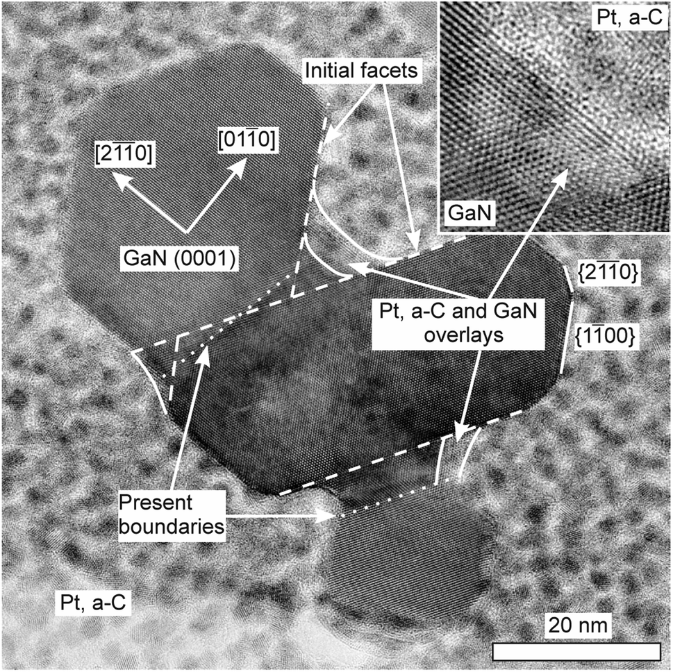 | ||
| Fig. 6 HRTEM micrograph of coalesced 2400 nm long NWs sectioned at a height of 200 nm. Solid, dotted and dashed lines show the facets of NWs, the present boundaries between them, and probable boundaries immediately after their coalescence, respectively. The inset shows a magnified micrograph revealing the superposition of the contrast of the GaN lattice and that of Pt and amorphous C. | ||
In the concave regions at the NW joint, a superposition of the contrasts of the GaN crystal lattice and that of the Pt nanoparticles deposited during specimen preparation is observed. The width of the superposition region between the two large NWs in Fig. 6 is about 5 nm, while the thickness of the foil, estimated by the comparison of the experimental and the simulated convergent-beam electron diffraction patterns of GaN,40,41 is about 20 nm. With such a rate of the lateral growth, the whole hollow region will be filled during further NW elongation after about 100 nm of axial growth. Then, the lateral growth will cease providing a common {100} facet of the merged NWs. The NW aggregate will then have a common hexagonal cross-sectional shape and grow further as a single NW. The neck between the large central NW in Fig. 6 and a small NW at the bottom of the figure is presumably a result of the filling of the gap between NWs below their joint. We thus suppose that this joint was at a height above the foil cut out for the TEM study.
Two samples identical to the ones shown in Fig. 5a and b have been recently studied by GISAXS.37 We revisit these measurements and perform new Monte Carlo simulations of the intensity with the aim to gain more detailed information on the cross sections of NWs. The GISAXS intensities from samples with NWs of 230 nm and 650 nm in length are presented in Fig. 7a, b, d and e, respectively. Since the GISAXS intensity I(qx) (where the x axis is along the surface in the direction normal to the incident X-ray beam) follows at large qx Porod's law I(qx)∝qx−4, the product I(qx)qx4 is plotted. The gray lines in Fig. 7a, b, d and e are the experimental curves from ref. 37. Red broken lines are Monte Carlo simulations that assume distorted hexagonal cross sections and take into account the distributions of the NW orientations and the cross-sectional shapes.37 These simulations adequately reproduce the scattering intensity in the direction of the normal to the {100} facets (facet truncation rods) for orientations of 0° and 60°, but give too low intensity in the direction of the NW edges, for an orientation of 30°. Hence, we refine the model with the aim to properly describe the scattering intensity in the direction of the edges between {100} facets.
 | ||
| Fig. 7 GISAXS intensity from samples with NW arrays of an average NW length of (a and b) 230 nm and (d and e) 650 nm (gray lines).37 The intensity curves are obtained at different azimuthal orientations of the samples from 0° to 60° with a step of 5°. Red dashed lines show Monte Carlo simulations assuming hexagonal cross-sectional shapes of NWs performed in ref. 37. Blue lines are the results of the Monte Carlo simulation allowing for dodecagonal cross sections with both {100} and {110} side facets. Examples of the NW cross sections used in the simulations of the two samples are presented in (c) and (f), respectively. | ||
For this purpose, we model the cross sections of NWs by hexagons with the vertices cut such as to represent the {110} facets. Hence, the cross-sectional shape, instead of a hexagon (a polygon with six vertices), becomes a dodecagon (a polygon with twelve vertices). Fig. 7c and f exemplify the cross-sectional distributions in the Monte Carlo simulations of the two samples. The disorder in NW orientations and cross-sectional shapes is modeled in the same way as in ref. 37, and random cuts of the hexagon vertices are added to the model. Since the scattering amplitude of an arbitrary polygon is expressed through coordinates of the vertices, the simulations are performed in the same way as described in ref. 37. The simulated GISAXS intensity curves for the two samples are shown in Fig. 7a, b, d and e by blue curves. The curves for the orientation of 30°, i.e., the {110} facet truncation rods, are now close to the experimental curves. We also found in the simulations a 1° misalignment of the samples with respect to the NW facets: the nominal orientations 0°, 30°, 60° in Fig. 7 are in fact 1°, 31°, 61° when counting from the mean orientations of the {100} facets. Particularly, the misalignment is clearly seen in comparison of the top pair of the experimental curves in Fig. 7d with the respective pair in Fig. 7e. The curves at 5° and 55° are expected to coincide due to the hexagonal symmetry. However, they differ since they correspond to 6° and 56° with respect to the facets. The root-mean-squared (rms) roughness of the NW sidewalls for the two samples is found to be 0.7 and 0.8 nm, respectively, somewhat smaller than the values obtained in the former study.37 These values are less than 3 times the height of an atomic step on the {100} facet.
The NW size distributions for the two samples obtained in the simulations are compared in Fig. 4a with the results of the TEM study. A good agreement is found, considering that GISAXS provides an average over the whole volume of the NWs while TEM represents their distribution at a certain height. Fig. 8 presents the distributions of the ratio of the areas of the {110} and {100} side facets of NWs obtained in the Monte Carlo simulations. The average ratios are 0.26 and 0.37 for the two samples. Hence, NWs with a larger length are more roundish, as it is seen when comparing Fig. 7c and f. This result agrees well with the TEM images of the respective samples shown in Fig. 5a and b.
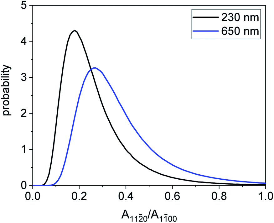 | ||
| Fig. 8 Distributions of the ratios of the areas of the {110} and {100} facets obtained in the Monte Carlo simulations of the GISAXS intensities. The NW distributions obtained in the simulations are exemplified in Fig. 7c and f. | ||
4 Discussion
The results of the previous section reveal two opposing trends in the shape evolution of the growing GaN NWs. At the top, merging NWs develop common {100} facets. In the lower parts, NWs attain roundish shapes containing both {100} and highly stepped {110} facets.
As the NWs grow in length, they bundle to reduce the energy of the side facets at the expense of the bending energy.19 The concave regions between merged NWs are filled by radial growth that reduces the total perimeter and thus the surface energy of NWs. The rate of the radial growth has been estimated from the observation of both the GaN crystal lattice and the Pt with amorphous C filling in the overlay region in Fig. 6. The width of this region of 5 nm in a 20 nm thick foil means that the whole concave region will be filled during the NW elongation of about 100 nm. Then, a common {100} facet will be formed. Such facets dominate in the cross-sectional shape at the NW top, as seen in Fig. 2d. The filling of the concave regions with the formation of {100} facets seems the main process responsible of the increase of the surface coverage by NWs in Fig. 3b from 0.2 at the end of the nucleation stage to 0.4 as the NWs reach 2.4 μm in length.
Further insight into the shape transformation follows from a comparison of the three plots in Fig. 3. After the nucleation process ends at the NW lengths of about 200 nm, the increase of the total area covered by NWs in Fig. 3b is accompanied with the decrease of their total perimeter in Fig. 3c. Such behavior cannot be achieved if NWs grow by scaling their cross-sectional dimensions. Rather, an overgrowth of the concave regions gives rise to the area increase together with the perimeter decrease.
A shape transformation of different kind takes place at a lower height. Fig. 5 shows that, as the NWs grow in length, they become more roundish at their bottom. Some NWs are almost perfectly round, as seen, for example, in the left bottom image in Fig. 5f. However, most of the NWs possesses notable {100} facets, connected by arcs with continuously varying surface orientation. A more detailed comparison of the magnified images in Fig. 5g and i also shows that the {100} oriented parts of the surfaces look differently. NWs of small length in Fig. 5d and g possess atomically flat side facets. Even individual atomic steps on the facets are recognized in the images, indicating that the columns of atoms run through the whole thickness of the TEM specimen. In contrast, the {100} oriented parts of the surface of long NWs in Fig. 5f and i are more diffuse, pointing to some roughness of the side facets.
In Fig. 1, besides the 2400 nm long NWs, we also observe short NWs with the lengths less than 500 nm. In fact, the NW length distribution is bimodal:42 during growth, a part of NWs is shadowed from the impinging fluxes and does not grow in length. Thus, some NWs observed in Fig. 2a and b may be these shorter NWs. They occur in the same environment as the bottom parts of the longer NWs and possess the same cross-sectional shapes. Hence, there is no need to consider them differently from the cross sections of long NWs at the same height.
The opposing trends of faceting in the top parts of NWs and rounding in the bottom parts can be attributed to the consequences of the very different NW environments at the top and the bottom. The top part of a NW is directly exposed to the Ga and N fluxes. In addition, Ga adatoms diffuse along the {100} side facets to the top (000) facet. These adatoms, together with the Ga adatoms directly impinging at the top facet, react with the N flux and thus give rise to the axial NW growth. In contrast, radial growth on the {100} side facets does not take place in the absence of Ga rich conditions on the top facet.43 Following the description of the shapes of GaN crystals grown by vapor phase epitaxy in terms of the kinetic Wulff construction,44–48 we conclude that in MBE growth of GaN NWs, a kinetic Wulff plot in the 0001 plane possesses a zero growth velocity in the 〈100〉 directions, which gives rise to the {100} faceted NWs in their growing parts.
The bottom parts of the NWs are shadowed from the impinging fluxes by surrounding NWs.42 They do not receive direct Ga and N fluxes and hence no radial growth can take place at the bottom. At the high substrate temperatures employed, GaN may dissociate and desorb, as it takes place for (0001)-oriented GaN films at or above 800 °C.49,50 However, the surface coverage observed for the bottom parts of the long NWs is virtually identical to that of the shorter NWs grown for shorter times as seen in Fig. 3b, and the sublimation of GaN, if any, must occur with a very low rate.
Different NW environments in the top and in the bottom parts, and different transformations of the cross-sectional shapes, are inherent to MBE growth and are not expected in vapor phase epitaxy. The shape evolution observed in our work is a result of the shadowing of NWs by their neighbors from the direct impinging atomic beams, which does not take place in the growth from a vapor. The equilibrium growth shapes observed in vapor phase epitaxy depend on temperature, pressure, and the source materials.48
The stability of {100} planes at high temperatures is confirmed by the GaN NW shape transformation during thermal decomposition.51 It has been found that the decomposition of GaN NWs is initiated at the edges between the top (0001) and the side {100} facets and proceeds layer-by-layer, with a rate at the {100} facets an order of magnitude lower than that at the (0001) facet. Such edges are absent at the bottom of the NWs studied in the present work and cannot serve as the starting point of the decomposition process. Further evidence of the stability of both {100} and {110} facets can be found in the selective area sublimation of pre-patterned GaN(0001) layers.52,53 In this technique, the GaN layer decomposes except in areas covered by a protective mask, until only GaN columns with straight sidewalls remain underneath the mask. In other words, desorption ceases as soon as the sides of the columns become vertical.
In the opposite case of the selective area growth of GaN NWs, the cross-sectional shape transformation is observed during NW growth after the initial nucleation and full coalescence within each nanohole.54 The NWs are initially roundish, then acquire both {100} and {110} facets, and finally become hexagonal with {100} facets only. This final shape is treated in ref. 54 as the equilibrium crystal shape. However, this shape is reached during growth under impinging Ga and N fluxes and hence has to be considered as the equilibrium growth shape. The angular dependency of the surface energy considered in ref. 54 has to be treated as the one of the growth velocity in the lateral plane.
Thus, we conclude that the cross sections of the NWs tend to attain the equilibrium crystal shape in the bottom parts of the NWs. The equilibrium crystal shape may contain flat facets as well as continuously curved regions between them, depending on the shape of the angular plot of the surface free energy.55 The ab initio calculations23–31 provide surface energies only for the low index {100} and {110} facets. These energies amount to values of about 100 meV Å−2 or slightly above, with the {100} surface energy lower than that of the {110} surface by about 5 meV Å−2. If the angular plot of the surface energies would have strong cusps in these directions, so that the equilibrium crystal shape consists only of these facets, the ratio of the areas of the {110} and {100} facets is about 0.5. The average values of 0.26 and 0.37 obtained in the GISAXS study of the samples with 230 nm and 650 nm long NWs (see Fig. 8) are smaller, since the GISAXS measurements present an average over the whole NW volume. A replacement of the curved regions of the NW surface with the {110} facets in the modeling of the GISAXS intensity is a reasonable simplification, especially because relatively short NWs with dominant {100} facets are modeled.
Finally, based on the observation of the {100} facets (smeared out by the oxidation of Ga) and curved parts of the surface between them at the bottom parts of long NWs, we conclude that the polar plot of the surface free energies contains cusps in the 〈100〉 directions and smooth minima in the 〈110〉 directions.
5 Summary
We found two opposing trends in the evolution of the cross-sectional shape of GaN NWs along their length during growth by MBE. The top parts of NWs merge together and develop common {100} side facets during further growth. Their formation proceeds under continuously impinging Ga and N fluxes and can be considered in terms of the kinetic Wulff construction as due to zero growth rate at the {100} facets. At the bottom parts of NWs, a transformation to a roundish shape with {100} facets and arcs due to smoothly varying surface orientation between them is observed. This transformation takes place in the absence of the impinging fluxes due to the shadowing of NWs by the surrounding ones and can be considered as a transition to the equilibrium cross-sectional crystal shape, presumably due to the fact that the bottom part of the NWs do not receive direct Ga and N fluxes, but are only annealed. The observed cross-sectional shape corresponds to the polar plot of the surface free energies with cusps in the 〈100〉 directions and smooth minima in the 〈110〉 directions.
Author contributions
SFG was responsible for the growth of GaN NW samples. RV and NIB performed the TEM study. OVK made the GISAXS measurements. VMK used Monte Carlo simulations to model the GISAXS experiment. VMK and OB analyzed the data. RV, VMK, and OB wrote the manuscript.Conflicts of interest
There are no conflicts to declare.Acknowledgements
We thank Carsten Stemmler (Paul-Drude-Institut, Berlin) for his help with the preparation of the samples and Lutz Geelhaar (Paul-Drude-Institut, Berlin) for a critical reading of the manuscript. We acknowledge the ESRF for providing the beamtime. RV and NIB acknowledge the partial financial support of the Ministry of Science and Higher Education of the Russian Federation (State assignment No. FSMR-2020-0018). SFG acknowledges the partial financial support received through the Spanish program Ramón y Cajal (co-financed by the European Social Fund) under grant RYC-2016-19509 from the former Ministerio de Ciencia, Innovación y Universidades.References
- F. Chen, X. Ji and S. P. Lau, Mater. Sci. Eng., R, 2020, 142, 100–578 Search PubMed.
- S. D. Hersee, A. K. Rishinaramangalam, M. N. Fairchild, L. Zhang and P. Varangis, J. Mater. Res., 2011, 26, 2293–2298 CrossRef CAS.
- K. Kishino and S. Ishizawa, Nanotechnology, 2015, 26, 225–602 CrossRef PubMed.
- R. Calarco, M. Marso, T. Richter, A. I. Aykanat, R. J. Meijers, A. V. D. Hart, T. Stoica and H. Lüth, Nano Lett., 2005, 5, 981–984 CrossRef CAS PubMed.
- T. Auzelle, M. Azadmand, T. Flissikowski, M. Ramsteiner, K. Morgenroth, C. Stemmler, S. Fernández-Garrido, S. Sanguinetti, H. T. Grahn, L. Geelhaar and O. Brandt, ACS Photonics, 2021, 8, 1718–1725 CrossRef CAS.
- V. M. Kaganer, O. Marquardt and O. Brandt, Nanotechnology, 2016, 27, 165201 CrossRef PubMed.
- J. Kamimura, P. Bogdanoff, P. Corfdir, O. Brandt, H. Riechert and L. Geelhaar, ACS Appl. Mater. Interfaces, 2016, 8, 34490–34496 CrossRef CAS PubMed.
- M. A. H. Khan and M. V. Rao, Sensors, 2020, 20, 3889 CrossRef CAS PubMed.
- J. Lin, W. Wang and G. Li, Adv. Funct. Mater., 2020, 2005677 CrossRef CAS.
- B. AlOtaibi, S. Fan, D. Wang, J. Ye and Z. Mi, ACS Catal., 2015, 5, 5342–5348 CrossRef CAS.
- Y. Wang, S. Fan, B. AlOtaibi, Y. Wang, L. Li and Z. Mi, Chem.–Eur. J., 2016, 22, 8809–8813 CrossRef CAS PubMed.
- T. Auzelle, F. Ullrich, S. Hietzschold, C. Sinito, S. Brackmann, W. Kowalsky, E. Mankel, O. Brandt, R. Lovrincic and S. Fernández-Garrido, ACS Appl. Mater. Interfaces, 2021, 13, 4626–4635 CrossRef CAS PubMed.
- A. Feduniewicz, C. Skierbiszewski, M. Siekacz, Z. R. Wasilewski, I. Sproule, S. Grzanka, R. Jakieła, J. Borysiuk, G. Kamler, E. Litwin-Staszewska, R. Czernecki, M. Boćkowski and S. Porowski, J. Cryst. Growth, 2005, 278, 443–448 CrossRef CAS.
- S. F. Chichibu, A. Setoguchi, A. Uedono, K. Yoshimura and M. Sumiya, Appl. Phys. Lett., 2001, 78, 28–30 CrossRef CAS.
- A. J. Ptak, L. J. Holbert, L. Ting, C. H. Swartz, M. Moldovan, N. C. Giles, T. H. Myers, P. Van Lierde, C. Tian, R. A. Hockett, S. Mitha, A. E. Wickenden, D. D. Koleske and R. L. Henry, Appl. Phys. Lett., 2001, 79, 2740–2742 CrossRef CAS.
- K. Y. Lai, T. Paskova, V. D. Wheeler, T. Y. Chung, J. A. Grenko, M. A. L. Johnson, K. Udwary, E. A. Preble and K. R. Evans, Phys. Status Solidi A, 2012, 209, 559–564 CrossRef CAS.
- S. Fernández-Garrido, J. Grandal, E. Calleja, M. A. Sánchez-García and D. López-Romero, J. Appl. Phys., 2009, 106, 126102 CrossRef.
- S. Fernández-Garrido, X. Kong, T. Gotschke, R. Calarco, L. Geelhaar, A. Trampert and O. Brandt, Nano Lett., 2012, 12, 6119–6125 CrossRef PubMed.
- V. M. Kaganer, S. Fernández-Garrido, P. Dogan, K. K. Sabelfeld and O. Brandt, Nano Lett., 2016, 16, 3717–3725 CrossRef CAS PubMed.
- O. Brandt, S. Fernández-Garrido, J. K. Zettler, E. Luna, U. Jahn, C. Chèze and V. M. Kaganer, Cryst. Growth Des., 2014, 14, 2246–2253 CrossRef CAS.
- K. A. Bertness, N. A. Sanford, J. M. Barker, J. B. Schlager, A. Roshko, A. V. Davydov and I. Levin, J. Electron. Mater., 2006, 35, 576–580 CrossRef CAS.
- L. Largeau, D. L. Dheeraj, M. Tchernycheva, G. E. Cirlin and J. C. Harmand, Nanotechnology, 2008, 19, 155704 CrossRef CAS PubMed.
- J. E. Northrup and J. Neugebauer, Phys. Rev. B: Condens. Matter Mater. Phys., 1996, 53, R10477 CrossRef CAS.
- D. Segev and C. G. Van der Walle, Surf. Sci., 2007, 601, L15–L18 CrossRef CAS.
- C. E. Dreyer, A. Janotti and C. G. Van der Walle, Phys. Rev. B: Condens. Matter Mater. Phys., 2014, 89, 081305(R) CrossRef.
- P. Mutombo and O. Romanyuk, J. Appl. Phys., 2014, 115, 203–508 CrossRef.
- R. González-Hernández, A. González-García and D. Barragán-Yani, Appl. Surf. Sci., 2014, 314, 794–799 CrossRef.
- H. Li, L. Geelhaar, H. Riechert and C. Draxl, Phys. Rev. Lett., 2015, 115, 085503 CrossRef PubMed.
- J. Zhang, Y. Zhang, K. Tse, B. Deng, H. Xu and J. Zhu, J. Appl. Phys., 2016, 119, 205–302 Search PubMed.
- Y. Zhang, J. Zhang and J. Zhu, Phys. Rev. Mater., 2018, 2, 073401 CrossRef CAS.
- T. Akiyama, Y. Seta, K. Nakamura and T. Ito, Phys. Rev. Mater., 2019, 3, 023401 CrossRef CAS.
- B. Heying, R. Averbeck, L. F. Chen, E. Haus, H. Riechert and J. S. Speck, J. Appl. Phys., 2000, 88, 1855–1860 CrossRef CAS.
- T. Kamino, T. Yaguchi, T. Hashimoto, T. Ohnishi and K. Umemura, in Introduction to Focused Ion Beams: Instrumentation, Theory, Techniques, and Practice, ed. L. A. Giannuzzi and F. A. Stevie, Springer, Boston, 2005, pp. 230–234 Search PubMed.
- R. L. Volkov, N. I. Borgardt, D. G. Gromov and S. V. Dubkov, J. Surf. Invest.: X-Ray, Synchrotron Neutron Tech., 2018, 12, 473–479 CrossRef CAS.
- Transmission Electron Microscopy: Diffraction, Imaging, and Spectrometry, ed. C. B. Carter and D. B. Williams, Springer, Switzerland, 2016 Search PubMed.
- J. Schindelin, I. Arganda-Carreras, E. Frise, V. Kaynig, M. Longair, T. Pietzsch, S. Preibisch, C. Rueden, S. Saalfeld, B. Schmid, J. Y. Tinevez, D. J. White, V. Hartenstein, K. Eliceiri, P. Tomancak and A. Cardona, Nat. Methods, 2012, 9, 676–682 CrossRef CAS PubMed.
- V. M. Kaganer, O. V. Konovalov and S. Fernández-Garrido, Acta Crystallogr., Sect. A: Found. Adv., 2021, 77, 42–53 CrossRef CAS PubMed.
- G. Renaud, R. Lazzari and F. Leroy, Surf. Sci. Rep., 2009, 64, 255–380 CrossRef CAS.
- C. Hauswald, P. Corfdir, J. K. Zettler, V. M. Kaganer, K. K. Sabelfeld, S. Fernández-Garrido, T. Flissikowski, V. Consonni, T. Gotschke, H. T. Grahn, L. Geelhaar and O. Brandt, Phys. Rev. B: Condens. Matter Mater. Phys., 2014, 90, 165304 CrossRef.
- P. A. Stadelmann, Ultramicroscopy, 1987, 21, 131–145 CrossRef CAS.
- M. Klinger, M. Němec, L. Polívka, V. Gärtnerová and A. Jäger, Ultramicroscopy, 2015, 150, 88–95 CrossRef CAS PubMed.
- K. K. Sabelfeld, V. M. Kaganer, F. Limbach, P. Dogan, O. Brandt, L. Geelhaar and H. Riechert, Appl. Phys. Lett., 2013, 103, 133105 CrossRef.
- S. Fernández-Garrido, V. M. Kaganer, K. K. Sabelfeld, T. Gotschke, J. Grandal, E. Calleja, L. Geelhaar and O. Brandt, Nano Lett., 2013, 13, 3274–3280 CrossRef PubMed.
- D. Du, D. J. Srolovitz, M. E. Coltrin and C. C. Mitchell, Phys. Rev. Lett., 2005, 95, 155503 CrossRef PubMed.
- Q. Sun, C. D. Yerino, T. S. Ko, Y. S. Cho, I.-H. Lee, J. Han and M. E. Coltrin, J. Appl. Phys., 2008, 104, 093523 CrossRef.
- V. Jindal and F. Shahedipour-Sandvik, J. Appl. Phys., 2009, 106, 083115 CrossRef.
- Q. Sun, C. D. Yerino, B. Leung, J. Han and M. C. Coltrin, J. Appl. Phys., 2011, 110, 053517 CrossRef.
- B. N. Bryant, A. Hirai, E. C. Young, S. Nakamura and J. S. Speck, J. Cryst. Growth, 2013, 369, 14–20 CrossRef CAS.
- N. Grandjean, J. Massies, F. Semond, S. Yu. Karpov and R. A. Talalaev, Appl. Phys. Lett., 1999, 74, 1854–1856 CrossRef CAS.
- S. Fernández-Garrido, G. Koblmüller, E. Calleja and J. S. Speck, J. Appl. Phys., 2008, 2008, 033541 CrossRef.
- J. K. Zettler, P. Corfdir, C. Hauswald, E. Luna, U. Jahn, T. Flissikowski, E. Schmidt, C. Ronning, A. Trampert, L. Geelhaar, H. T. Grahn, O. Brandt and S. Fernández-Garrido, Nano Lett., 2016, 16, 973–980 CrossRef CAS PubMed.
- B. Damilano, S. Vézian, J. Brault, B. Alloing and J. Massies, Nano Lett., 2016, 16, 1863–1868 CrossRef CAS PubMed.
- S. Fernández-Garrido, T. Auzelle, J. Lähnemann, K. Wimmer, A. Tahraoui and O. Brandt, Nanoscale Adv., 2019, 1, 1893–1900 RSC.
- Ž. Gačević, D. G. Sánchez and E. Calleja, Nano Lett., 2015, 15, 1117–1121 CrossRef PubMed.
- C. Herring, Phys. Rev., 1951, 82, 87–93 CrossRef CAS.
Footnotes |
| † Electronic supplementary information (ESI) available: Quantification of the transmission electron microscopy images. See DOI: 10.1039/d1na00773d |
| ‡ Present address: Grupo de electrónica y semiconductors, Dpto. Física Aplicada and Instituto Nicolás Cabrera, Universidad Autónoma de Madrid, C/Francisco Tomás y Valiente 7, 28049 Madrid, Spain. |
| This journal is © The Royal Society of Chemistry 2022 |