
 Open Access Article
 This Open Access Article is licensed under a
 Creative Commons Attribution 3.0 Unported Licence
Custom-made holey graphene via scanning probe block co-polymer lithography†
Samar A.
Alsudir
 a,
Roa S.
Fardous
a,
Shahla
Alsoughayer
b,
Abdulaziz M.
Almalik
ab,
Edreese H.
Alsharaeh
c and
Ali H.
Alhasan
*cd
a,
Roa S.
Fardous
a,
Shahla
Alsoughayer
b,
Abdulaziz M.
Almalik
ab,
Edreese H.
Alsharaeh
c and
Ali H.
Alhasan
*cd
aNational Center for Pharmaceutical Technology, Life Science and Environmental Research Institute, King Abdulaziz City for Science and Technology (KACST), P. O. Box 6086, Riyadh 11461, Saudi Arabia
bKACST-BWH/Harvard Centre of Excellence for Biomedicine, Joint Centers of Excellence Program, King Abdulaziz City for Science and Technology (KACST), P. O. Box 6086, Riyadh 11461, Saudi Arabia
cCollege of Science and General Studies, Alfaisal University, P. O. Box 50927, Riyadh 11533, Saudi Arabia
dNational Center for Biotechnology, Life Science and Environmental Research Institute, King Abdulaziz City for Science and Technology (KACST), P. O. Box 6086, Riyadh 11461, Saudi Arabia. E-mail: aalhasan@kacst.edu.sa
First published on 31st January 2022
Abstract
Oxidative chemical etching of metal nanoparticles (NPs) to produce holey graphene (hG) suffers from the presence of aggregated NPs on the graphene surface triggering heterogeneous etching rates and thereby producing irregular sized holes. To encounter such a challenge, we investigated the use of scanning probe block co-polymer lithography (SPBCL) to fabricate precisely positioned silver nanoparticles (AgNPs) on graphene surfaces with exquisite control over the NP size to prevent their aggregation and consequently produce uniformly distributed holes after oxidative chemical etching. SPBCL experiments were carried out via printing an ink suspension consisting of poly(ethylene oxide-b-2-vinylpyridine) and silver nitrate on a graphene surface in a selected pattern under controlled environmental and instrumental parameters followed by thermal annealing in a gaseous environment to fabricate AgNPs. Scanning electron microscopy revealed the uniform size distribution of AgNPs on the graphene surface with minimal to no aggregation. Four main sizes of AgNPs were obtained (37 ± 3, 45 ± 3, 54 ± 2, and 64 ± 3 nm) via controlling the printing force, z-piezo extension, and dwell time. Energy dispersive X-ray spectroscopy analysis validated the existence of elemental Ag on the graphene surface. Subsequent chemical etching of AgNPs using nitric acid (HNO3) with the aid of sonication and mechanical agitation produced holes of uniform size distribution generating hG. The obtained ID/IG ratios ≤ 0.96 measured by Raman spectroscopy were lower than those commonly reported for GO (ID/IG > 1), indicating the removal of more defective C atoms during the etching process to produce hG while preserving the remaining C atoms in ordered or crystalline structures. Indeed, SPBCL could be utilized to fabricate uniformly distributed AgNPs of controlled sizes on graphene surfaces to ultimately produce hG of uniform hole size distribution.
Introduction
Among various carbon nanostructures, holey graphene (hG) has attracted considerable interest owing to its exceptional properties including excellent electrical conductivity, large specific surface area, and superior chemical/electrochemical stability surpassing its pristine graphene form.1,2 It is synthesized via perforating abundant in-plane pores using either bottom-up3–5 or top-down6–8 methodologies, among which the so-called template-assisted or template-free approaches are the most common. The latter approach operates via oxidative chemical etching of graphene using either oxidants such as H2O2,6,7 O2,9 nitric acid (HNO3),10 and potassium hydroxide (KOH),11 or catalysts including metal (Ag12–14 and Cu15) or metal oxide (ZnO,16 MnO2,17 SnO2,18 and Fe2O3)19 nanoparticles (NPs). The catalytic etching process involves NP deposition on the graphene basal plane, etching reaction, and catalyst removal. The deposited NPs could catalytically oxidize C atoms to produce nano-sized holes under specific conditions such as annealing or photochemical/sonochemical treatments. Although graphene is used as a mesh to enhance NP distribution, aggregation still persists,12,20–23 which is a hammering obstacle resulting in heterogeneous etching rates24,25 and thereby producing irregular sized holes.15,26 Therefore, advanced methodologies for fabricating hG with tunable hole sizes are coveted.Inspired by the successful route of scanning probe block co-polymer lithography (SPBCL) to fabricate precisely positioned single metallic NPs with control over the particle size,27–30 we hypothesized the use of SPBCL to fabricate hG with enhanced hole distribution. SPBCL might offer an exquisite control over the size and position of the resulting nanoholes on graphene surfaces (Scheme 1).
 | ||
| Scheme 1 Proposed SPBCL route to fabricate hG. | ||
Graphene hydrophobicity,31 thermal stability (≤600 °C),32 and electrical conductivity33 are the determinant properties that could permit the use of SPBCL to fabricate uniformly distributed AgNPs on its surface. Subsequent chemical etching of patterned AgNPs is expected to create patterned nanoholes on graphene with high uniformity.
Experimental
Materials
Dettol hand soap (DHS) (original) was bought from a nearby grocery store. Ethanol (EtOH) and hexane were purchased from Fisher Scientific, Ltd., UK. Graphene substrates (monolayer graphene on Si/SiO2 substrates (2.5 × 2.5 cm2)) were obtained from Graphena, Inc., Spain. Graphite in powder form was purchased from Sigma-Aldrich, USA. HNO3 was bought from Panreac Química SLU, Spain. Hexamethyldisilazane (HMDS) was obtained from Alfa Aesar, USA. Poly(ethylene oxide-b-2-vinylpyridine) (PEO-b-P2VP) (Mn: PEO 2800 and P2VP 1500) was obtained from Polymer Source, Inc., Canada. Polyvinylpyrrolidone (PVP) (Mw: 1![[thin space (1/6-em)]](https://www.rsc.org/images/entities/char_2009.gif) 300000) and silver nitrate (AgNO3) were purchased from Sigma-Aldrich, USA. Milli-Q® distilled deionized water (DDW) was used throughout the course of the investigation.
300000) and silver nitrate (AgNO3) were purchased from Sigma-Aldrich, USA. Milli-Q® distilled deionized water (DDW) was used throughout the course of the investigation.
Printing process
Si/SiO2 substrates (2 × 2 cm2) and polydimethyl siloxane (PDMS) pen arrays with a 100 μm tip-spacing were purchased from TERA-Print, LLC., USA. In a typical experiment, a Si/SiO2 substrate was vapor primed with an HMDS:hexane mixture (1:1 v/v) for 24 h under static vacuum to render the surface hydrophobic.34 Following a procedure developed by Noroozi et al.35 with slight modification, graphene was exfoliated out of graphite (1 mg mL−1) upon mixing with PVP (0.9 mg mL−1) and DHS (12.50 μL mL−1) in DDW (4 mL) with the aid of probe sonication in a continuous mode at 60% amplitude at various sonication times (1–4 h). To self-assemble graphene flakes into a uniform layer, graphene in PVP:DHS (1 mL) was diluted with EtOH (5 mL), sonicated for 15 min, and then injected in a timely manner into DDW (12 mL). The self-assembled layer was next carefully transferred to the HMDS-primed substrate and allowed to dry under ambient conditions. The ink was prepared via dissolving PEO-b-P2VP (5 mg mL−1) in DDW under continuous stirring till a transparent solution was obtained. Subsequently, AgNO3 (0.5 mM) was added and the pH was adjusted to 3 using HNO3. The ink was kept under stirring for 3 h in the dark prior to the electrospraying process. A PDMS pen array was plasma cleaned using a Zepto plasma cleaner (Diener Electronic-Germany, O2 plasma, 18 psi, 120 W, 220 s) directly before ink deposition via electrospraying using a Spraybase® instrument (Spraybase®-Ireland, emitter inner diameter: 0.35 mm, flow rate: 1 mL h−1, distance from the injector to the collector: 10 cm, voltage: 8.4 kV, and duration of electrospraying: 10 min). SPBCL experiments were carried out on a TERA-Fab M series instrument, TERA-Print, LLC., USA, operating at a temperature of 27 ± 2 °C and a relative humidity (RH) of 92 ± 2%. Patterns of 12 × 12 dots were created with a step size of either 0.5 μm or 1 μm and variable dwell times (s) and z-piezo extensions (μm) while keeping the printing force constant at 200 mN. Annealing was carried out using a tube furnace (Lindberg/Blue M™ 1200 °C Split-Hinge, Thermo Scientific™, USA) having multiple gas ports to attach cylinders of Ar and H2.
Chemical etching process
Each printed substrate was dipped in an HNO3 aqueous solution (2.5 M), sonicated, and shaken for predetermined periods of time, after which the substrate was allowed to dry under ambient conditions.Characterization
The samples were analysed using the following characterization techniques: UV-Vis spectroscopy (PerkinElmer spectrometer-Lambda 950), thermogravimetric analysis (TGA) (NETZCH 209 F1 Thermo-gravimetric analyzer), Raman spectroscopy (Thermo DXR3 Raman Microscope), and scanning electron microscopy (SEM) (JEOL SEM-JSM-IT500HR-equipped with different detectors: an energy dispersive X-ray spectroscopy (EDS) detector, secondary electron detector (SED), and backscattering detector (BED)). The EDS detector is used to measure the spectrum of generated X-rays to determine the elements present in the sample (qualitative analysis) along with tracking the amount of each element from the intensity of the characteristic X-ray signals (quantitative analysis). The BED conveys information on the sample's composition wherein the number of backscattered electrons reaching the detector is proportional to the atom's Z (atomic) number. Higher Z atoms scatter more electrons back towards the detector than lower Z atoms and thus create higher signals. For example, the heavier Ag atoms (Z = 47) scatter more electrons than the lighter C (Z = 6) or O (Z = 8) atoms and thus appear brighter in the SEM images recorded using the BED. In contrast, the SED conveys topographic information of the sample surface as it detects secondary electrons originating from the surface or near-surface regions of the sample owing to the inelastic interactions between the primary electron beam and the sample.Image processing
Each SEM image was processed using the SEM software (SEM Operation), wherein the ruler tool was used to quantitatively measure the sizes of all AgNPs/formed holes. A line was drawn by tapping the start point of the target NP/hole and dragging the line to the end point of the target. Once done, the size will be displayed. This process was repeated for all NPs/holes in order to calculate the average size and standard deviation. The relative area of holes to that of graphene was calculated using ImageJ software.Results and discussion
SPBCL is increasingly becoming a preferred route to fabricate metal NPs owing to its vast capabilities to exquisitely control the size, shape, and position of NPs on solid substrates. SPBCL-defined polymeric nanoreactors govern the size of fabricated features via confining NP nucleation and growth, which are primarily affected by the hydrophobicity of the substrate, the printing force, z-piezo extension, and dwell time along with the conditions utilized during the subsequent thermal annealing step.36Si/SiO2 substrates were primed with HMDS via vapor coating of an HMDS:hexane mixture to ensure substrate hydrophobicity.34 To uniformly deposit graphene flakes on HMDS-primed substrates, graphene was first exfoliated out of graphite following a procedure developed by Noroozi et al.35 with slight modification. Briefly, graphite was suspended in a PVP:DHS aqueous dispersion with the aid of probe sonication as shown in Fig. 1a. Probe sonication was carried out in a continuous mode at 60% amplitude at various sonication times (1–4 h) to examine the output graphene flakes against a commercially available graphene suspended in the PVP:DHS aqueous dispersion and probe sonicated for 1 h. The UV-Vis spectrum of commercial graphene shown in Fig. 1b revealed the characteristic absorbance peak of graphene centered around 270 nm corresponding to the π/π* transitions of the aromatic C![[double bond, length as m-dash]](https://www.rsc.org/images/entities/char_e001.gif) C bonds along with a shoulder around 320 nm attributed to n/π* transitions of CO bonds present in graphene oxide.37 A gradual increase in absorption around 270 nm was found with increasing probe sonication time, 3 h of which exhibited a comparable absorbance to that of commercial graphene with a slight red-shifting indicating the preservation of the electronic conjugation within the graphene basal plane.38 Thereby, 3 h-probe sonication was applied hereafter to obtain exfoliated graphene flakes in the PVP:DHS aqueous dispersion. Next, a uniform layer of graphene flakes was deposited on the HMDS-primed substrate via Marangoni self-assembly described by Ye et al.39 Briefly, graphene in PVP:DHS was diluted with EtOH and sonicated for 15 min to ensure the uniformity of graphene flakes, which allowed their injection in a timely manner into DDW. Besides graphene hydrophobicity, the difference in surface tension between EtOH and DDW permitted graphene flakes to float, collide, and self-assemble to ultimately form a continuous layer of graphene in a uniform fashion. This layer was carefully transferred to the HMDS-primed substrate and allowed to dry under ambient conditions (Fig. 1c) in order to be subsequently used for the SPBCL experiment.
C bonds along with a shoulder around 320 nm attributed to n/π* transitions of CO bonds present in graphene oxide.37 A gradual increase in absorption around 270 nm was found with increasing probe sonication time, 3 h of which exhibited a comparable absorbance to that of commercial graphene with a slight red-shifting indicating the preservation of the electronic conjugation within the graphene basal plane.38 Thereby, 3 h-probe sonication was applied hereafter to obtain exfoliated graphene flakes in the PVP:DHS aqueous dispersion. Next, a uniform layer of graphene flakes was deposited on the HMDS-primed substrate via Marangoni self-assembly described by Ye et al.39 Briefly, graphene in PVP:DHS was diluted with EtOH and sonicated for 15 min to ensure the uniformity of graphene flakes, which allowed their injection in a timely manner into DDW. Besides graphene hydrophobicity, the difference in surface tension between EtOH and DDW permitted graphene flakes to float, collide, and self-assemble to ultimately form a continuous layer of graphene in a uniform fashion. This layer was carefully transferred to the HMDS-primed substrate and allowed to dry under ambient conditions (Fig. 1c) in order to be subsequently used for the SPBCL experiment.
 | ||
| Fig. 1 (a) Schematic of graphene exfoliation out of graphite using a DHS:PVP aqueous dispersion with the aid of probe sonication, (b) UV-Vis spectra of graphene dispersions obtained at different probe sonication times, and (c) SEM micrographs of the Marangoni self-assembly of graphene. | ||
In parallel to substrate preparation, the ink was prepared via dissolving PEO-b-P2VP in DDW at a concentration of 5 mg mL−1 followed by the addition of AgNO3 (0.5 mM). The pH was adjusted to 3 using HNO3, and the ink was kept under stirring in the dark for 3 h to ensure the complete coordination between the pyridine group and Ag ions. PEO-b-P2VP is expected to form micelles in DDW with P2VP core and PEO shell. The hydrophobic core coordinates with metal precursors while the hydrophilic shell ensures ink fluidity during printing in a high humidity environment. The ink was next electrosprayed on the polymer pen array and allowed to dry prior to mounting on the instrument. The sprayed polymer pen array was incubated for 2 hours in a high humidity environment (92 ± 2%) at 27 ± 2 °C prior to the printing process. This step is necessary to enable ink hydration, spreading, and diffusion, thereby facilitating its transport to the substrate. A 12 × 12 dot matrix design was used to print the ink using 200 mN of force, 1 s of dwell time, and a step size of 500 nm. Printing and patterning parameters are summarized in Table 1.
| Printing parameters | Patterning parameter | |||
|---|---|---|---|---|
| Force | 200 mN | X | Y | |
| Voltage | 10 V | Start point | 5 μm | 5 μm |
| Current threshold | 0.2 mA | Step size | 500 nm | 500 nm |
| Dwell time | 1 s | No. of points | 12 | 12 |
| Relative z-piezo extension | 0 μm | Spacing between pens | 100 μm | 100 μm |
The printed substrate was thermally annealed at 150 °C for 16 h under Ar atmosphere and then at 500 °C for another 16 h under H2. The first annealing stage induced AgNO3 particle nucleation and coarsening as the decomposition of AgNO3 wouldn't start unless the temperature reaches ∼285 °C. The second annealing stage initiated reduction and particle growth producing AgNPs29 along with decomposition of PEO-b-P2VP, PVP, and DHS since their decomposition temperatures are 409 °C,40 436 °C, and 289 °C (Fig. S1†), respectively. SEM micrographs shown in Fig. 2a–c reveal the uniform size distribution of AgNPs with an average of 38 ± 13 nm on graphene flakes. EDS analysis confirmed the presence of elemental Ag as shown in Fig. 2d. Subsequent chemical etching of AgNPs using HNO3 (2.5 M) under sonication for 6 h resulted in no obvious hole formation probably because the holes were too small to be seen and/or the contrast was too weak as shown in Fig. 3a and b. Thus, mechanical agitation was carried out for a week while monitoring the hole formation on a daily basis. On day 7, hG with uniformly distributed holes with an average size of 152 ± 45 nm was produced (Fig. 3c).
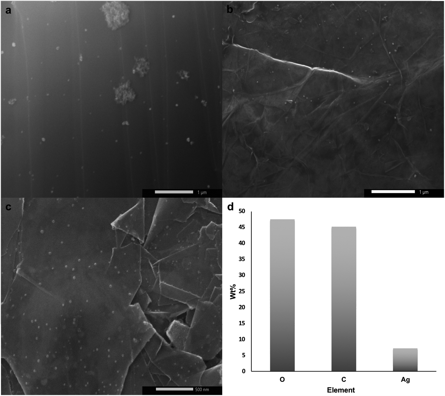 | ||
| Fig. 2 (a–c) SEM micrographs of the uniformly distributed AgNPs on graphene flakes, and (d) EDS analysis of Ag–graphene flakes. | ||
 | ||
| Fig. 3 SEM micrographs of etched AgNP-decorated graphene after (a and b) sonication for 6 h, and (c) mechanical agitation for a week. | ||
AgNPs acted as a catalyst to oxidize the surrounding carbon atoms resulting in CO/CO2 liberation and hole generation. This is generally accompanied by ‘track-marks’ formation owing to the etching-induced motion of AgNPs.12,13 Apparently, the holes' size is 4× larger than the size of AgNPs, which can be attributed to hole merging and/or excessive oxidative etching owing to the prolonged etching time.
After proven successful, the SPBCL approach was re-utilized to fabricate AgNPs of tunable sizes on a CVD-graphene substrate in order to lessen the number of steps and simplify the whole process. The same methodology for ink preparation, electrospraying, and humidification was followed. Yet, a 12 × 12 dot matrix design was used to print the ink dispersion via applying 200 mN of force, varied dwell times (3–6 s), varied relative z-piezo extensions (0–6 μm), and a step size of 1 μm in both X & Y directions as shown in Fig. 4a and summarized in Table 2. These variations in z-piezo extensions and dwell times would influence the size of the resulting AgNPs; the (0 μm, 3 s) block would result in fabricating the smallest NPs whereas the (6 μm, 6 s) block would account for the largest NPs.
 | ||
| Fig. 4 (a) Pattern of the dot matrix used for printing the ink dispersion on a CVD graphene substrate at 92 ± 2% RH and 27 ± 2 °C, (b) light microscope images of the CVD-graphene substrate right after ink printing, (c) plot representing the sizes of fabricated AgNPs on the CVD-graphene substrate upon varying the relative z-piezo extension and dwell time, and (d) fabricated AgNPs on the CVD-graphene substrate. | ||
| Printing parameters | Patterning parameter | |||
|---|---|---|---|---|
| Force | 200 mN | X | Y | |
| Voltage | 10 V | Start point | 5 μm | 5 μm |
| Current threshold | 0.2 mA | Step size | 1 μm | 1 μm |
| Dwell time | 3–6 s | No. of points | 12 | 12 |
| Relative z-piezo extension | 0–6 μm | Spacing between pens | 100 μm | 100 μm |
These instrumental parameters could have a pronounced effect on the amount of delivered ink to the substrate; increasing the relative z-piezo extension could increase the tip-substrate contact area and thereby increase the amount of delivered ink. Parallel to this, prolonged dwell times deliver larger amounts of ink to the substrate. Thereby, a tunable gradient of feature sizes was fabricated via varying the relative z-piezo extension and dwell time as evidenced in Fig. 4b. The printed CVD-graphene substrate was next thermally annealed under Ar atmosphere at 200 °C for 10 h and then at 500 °C for another 6 h. Four main populations of NPs ranging between 37 ± 3 nm and 64 ± 3 nm were observed owing to the applied variations in both the z-piezo extension and dwell time (Fig. 4c). Apparently, the fabricated AgNPs were of uniform size distribution on the CVD-graphene substrate showing no signs of aggregation (Fig. 4d). Indeed, the SPBCL approach adopted here evokes exquisite control over the size of the fabricated NPs on the CVD-graphene substrate via controlling the printing force, z-piezo extension, and dwell time.
Despite their uniform size distribution, AgNPs lost their patterned spatial features. This can be attributed to the partial loss of graphene hydrophobicity in the thermal annealing step, leading to the formation of multiple NPs per nanoreactor. Boosting graphene hydrophobicity via chemical means prior to the printing process might tremendously help in overcoming this encountered challenge. Another obstacle is the presence of defects in the CVD-graphene substrate including grafolds, in which AgNPs were trapped resembling the beads in a chain. Subsequent etching of AgNPs using HNO3 (2.5 M) with the aid of sonication for 4 h and shaking for another 14 h helped with the guided breakage of the graphene sheet into smaller structures owing to the presence of catalytic AgNP chains specifically in the grafolds (Fig. 5).
 | ||
| Fig. 5 SEM micrographs of the broken CVD-graphene sheet into smaller structures containing AgNPs owing to sonomechanical treatment in the presence of HNO3. Images on the left were taken using the secondary electron detector (SED) whereas those on the right are the representative images taken using the backscattering detector (BED). | ||
Prolonged etching (8 h of sonication and 28 h of shaking) produced either hG sheets (Fig. 6a) or two-dimensional laminar porous graphene (Fig. 6b) owing to the removal of AgNPs producing holes and subsequently stacked hG sheets. Similar to hG flakes, holes could be observed in both hG sheets and the two-dimensional laminar porous graphene exhibiting four main populations ranging between 207 ± 43 nm and 411 ± 63 nm. The relative area of holes to that of the graphene sheet was calculated to be 85 ± 8%.
 | ||
| Fig. 6 SEM micrographs (left) and schematics (right) of (a) an hG sheet, and (b) two-dimensional laminar porous graphene. | ||
Despite their holey structures, both hG flakes and sheets considerably retained their two-dimensional graphitic crystallinity as evidenced in Fig. 7. Raman spectra showed a D band at ∼1420 cm−1, a G band at ∼1630 cm−1, and a 2D band at ∼2763 cm−1. The obtained ID/IG ratios for hG flakes (0.89) and hG sheets (0.96) were lower than those commonly reported for GO (ID/IG > 1). This plausibly stemmed from removing more defective C atoms during the etching process to produce hG while preserving the remaining C atoms in ordered or crystalline structures despite the increase in the hole diameter.41,42
 | ||
| Fig. 7 Raman spectra of hG flakes and an hG sheet. | ||
The graphene surface could be primed with N-methyl-2-pyrrolidone (NMP) followed by HMDS43 to protect its conductivity during the printing step as well as its hydrophobicity during thermal annealing. This would further enhance the size and distribution of AgNPs on the graphene surface, if needed. The downstream etching step could be optimized to improve the size of holes via adjusting the sonication/shaking time along with the HNO3 concentration or employing oxygen plasma as an alternative etchant.
Conclusion
Graphene physiochemical properties including hydrophobicity, thermal stability, and electrical conductivity permitted the use of SPBCL to fabricate uniformly distributed AgNPs on its surface with minimal to no aggregation. Regardless of all encountered challenges, the developed SPBCL approach elicited a precise control over the size and position of the fabricated AgNPs on the graphene surface and hence producing hG of uniform hole size distribution after HNO3-induced etching. Indeed, SPBCL could be used to fabricate custom-made metal NP–graphene composites and/or their etched counterparts with spatial and dimensional control, offering a powerful route to nanofabrication and nanomanipulation bypassing the implementation of conventional methods. The produced hG might exhibit promising properties featuring high conductivity and hence it can be used in electronics, energy storage devices, and electro-catalytic reactions. Also, it can be potentially applied in biomedical applications either in the detection or the treatment of diseases.Author contributions
S. A. A., E. H. A., and A. H. A. designed the research; S. A. A., R. S. F., and S. A. performed the research; S. A. A. and A. H. A. analyzed the data; and S. A. A., E. H. A., A. M. A., and A. H. A. wrote and finalized the manuscript.Conflicts of interest
There are no competing interests to declare.Acknowledgements
This work was supported by the National Industrial Development and Logistics Program (NIDLP) part of the Saudi Vision 2030 through King Abdulaziz City for Science and Technology (KACST). S. A. A., A. M. A., and A. H. A. gratefully acknowledge the support from the International Institute of Nanotechnology at Northwestern University for the training on the TERA-Fab M series. Special thanks goes to Dr Ahmad Alshimmari and Abdulaziz Alsaiegh for their help with the tube furnace.References
- Y. Lin, Y. Liao, Z. Chen and J. W. Connell, Holey graphene: a unique structural derivative of graphene, Mater. Res. Lett., 2017, 5, 209 CrossRef CAS.
- A. C. Lokhande, A. Qattan, C. D. Lokhande and S. P. Patole, Holey graphene: an emerging versatile material, J. Mater. Chem. A, 2020, 8, 918 RSC.
- M. Wang, L. Fu, L. Gan, C. Zhang, M. Rümmeli, A. Bachmatiuk, K. Huang, Y. Fang and Z. Liu, CVD growth of large area smooth-edged graphene nanomesh by nanosphere lithography, Sci. Rep., 2013, 3, 1238 CrossRef PubMed.
- X. Dong, N. Hu, L. Wei, Y. Su, H. Wei, L. Yao, X. Li and Y. Zhang, A new strategy to prepare N-doped holey graphene for high-volumetric supercapacitors, J. Mater. Chem. A, 2016, 4, 9739 RSC.
- C. Moreno, M. Vilas-Varela, B. Kretz, A. Garcia-Lekue, M. V. Costache, M. Paradinas, M. Panighel, G. Ceballos, S. O. Valenzuela, D. Peña and A. Mugarza, Bottom-up synthesis of multifunctional nanoporous graphene, Science, 2018, 360, 199 CrossRef CAS PubMed.
- Y. Xu, Z. Lin, X. Zhong, X. Huang, N. O. Weiss, Y. Huang and X. Duan, Holey graphene frameworks for highly efficient capacitive energy storage, Nat. Commun., 2014, 5, 4554 CrossRef CAS PubMed.
- Y. Xu, C. Y. Chen, Z. Zhao, Z. Lin, C. Lee, X. Xu, C. Wang, Y. Huang, M. I. Shakir and X. Duan, Solution Processable Holey Graphene Oxide and Its Derived Macrostructures for High-Performance Supercapacitors, Nano Lett., 2015, 15, 4605 CrossRef CAS PubMed.
- A. K. Lu, H. Y. Li and Y. Yu, Holey graphene synthesized by electrochemical exfoliation for high-performance flexible microsupercapacitors, J. Mater. Chem. A, 2019, 7, 7852 RSC.
- P. Z. Shuangyan, G. Liqin, D. Zonghuai and L. Z. Lei, Green synthesis of holey graphene sheets and their assembly into aerogel with improved ion transport property, Electrochim. Acta, 2016, 212, 171 CrossRef.
- X. Wang, L. Jiao, K. Sheng, C. Li, L. Dai and G. Shi, Solution-processable graphene nanomeshes with controlled pore structures, Sci. Rep., 2013, 3, 1996 CrossRef PubMed.
- S. Wu, K. S. Hui, K. N. Hui, J. M. Yun and K. H. Kim, A novel approach to fabricate carbon sphere intercalated holey graphene electrode for high energy density electrochemical capacitors, Chem. Eng. J., 2017, 317, 461 CrossRef CAS.
- Y. Lin, K. A. Watson, J. W. Kim, D. W. Baggett, D. C. Working and J. W. Connell, Bulk preparation of holey graphene via controlled catalytic oxidation, Nanoscale, 2013, 5, 7814 RSC.
- E. Alsharaeh, F. Ahmed, Y. Aldawsari, M. Khasawneh, H. Abuhimd and M. Alshahrani, Novel synthesis of holey reduced graphene oxide (HRGO) by microwave irradiation method for anode in lithium-ion batteries, Sci. Rep., 2016, 6, 29854 CrossRef CAS PubMed.
- C. Guo, Y. Zhang, T. Zeng, D. Huang, Q. Wan and N. Yang, High-performance asymmetric supercapacitors using holey graphene electrodes and redox electrolytes, Carbon, 2020, 157, 298 CrossRef CAS.
- D. Dutta, J. Y. Jiang, A. Jamaluddin, S. M. He, Y. H. Hung, F. Chen, J. K. Chang and C. Y. Su, Nanocatalyst-assisted fine tailoring of pore structure in holey-graphene for enhanced performance in energy storage, ACS Appl. Mater. Interfaces, 2019, 11, 36560 CrossRef CAS PubMed.
- O. Akhavan, Graphene nanomesh by ZnO nanorod photocatalysts, ACS Nano, 2010, 4, 4174 CrossRef CAS PubMed.
- Z. Fan, Q. Zhao, T. Li, J. Yan, Y. Ren, J. Feng and T. Wei, Easy synthesis of porous graphene nanosheets and their use in supercapacitors, Carbon, 2012, 50, 1699 CrossRef CAS.
- H. K. Kim, S. M. Bak, S. W. Lee, M. S. Kim, B. Park, S. C. Lee, Y. J. Choi, S. C. Jun, J. T. Han, K. W. Nam, K. Y. Chung, J. Wang, J. Zhou, X. Q. Yang, K. C. Roh and K. B. Kim, Scalable fabrication of micron-scale graphene nanomeshes for high-performance supercapacitor applications, Energy Environ. Sci., 2016, 9, 1270 RSC.
- C. Ma, Y. Zhao and Y. Li, A facile solution-free etching preparation of porous graphene nanosheets with high performances for lithium storage, Chem. Eng. J., 2017, 320, 283 CrossRef CAS.
- Z. Jin, D. Nackashi, W. Lu, C. Kittrell and J. M. Tour, Tour Decoration, Migration, and Aggregation of Palladium Nanoparticles on Graphene Sheets, Chem. Mater., 2010, 22, 5695 CrossRef CAS.
- M. K. Chuang, S. W. Lin, F. C. Chen, C. W. Chu and C. S. Hsu, Gold nanoparticle-decorated graphene oxides for plasmonic-enhanced polymer photovoltaic devices, Nanoscale, 2014, 6, 1573 RSC.
- A. H. Alhasan, R. S. Fardous, S. A. Alsudir, M. A. Majrashi, W. M. Alghamdi, E. H. Alsharaeh and A. M. Almalik, Polymeric reactor for the synthesis of superparamagnetic-thermal treatment of breast cancer, Mol. Pharm., 2019, 16, 3577 CrossRef CAS PubMed.
- K. Garg, P. Papponen, A. Johansson, N. Puttaraksa and L. Gilbert, Preparation of graphene nanocomposites from aqueous silver nitrate using graphene oxide's peroxidase-like and carbocatalytic properties, Sci. Rep., 2020, 10, 5126 CrossRef CAS PubMed.
- P. Dixit and J. Miao, Effect of SF6 flow rate on the etched surface profile and bottom grass formation in deep reactive ion etching process, J. Phys.: Conf. Ser., 2006, 34, 095 CrossRef.
- H. Le-The, E. Berenschot, R. M. Tiggelaar, N. R. Tas, A. V. D. Berg and J. C. T. Eijkel, Large-scale fabrication of highly ordered sub-20 nm noble metal nanoparticles on silica substrates without metallic adhesion layers, Microsyst. Nanoeng., 2018, 4, 1 CrossRef CAS PubMed.
- T. Liu, L. Zhang, B. Cheng, X. Hu and J. Yu, Holey Graphene for Electrochemical Energy Storage, Cell Rep. Phys. Sci., 2020, 1, 100215 CrossRef CAS.
- J. Chai, F. Huo, Z. Zheng, L. R. Giam, W. Shim and C. A. Mirkin, Scanning probe block copolymer lithography, Proc. Natl. Acad. Sci. U. S. A., 2010, 107, 20202 CrossRef CAS PubMed.
- P. C. Chen, G. Liu, Y. Zhou, K. A. Brown, N. Chernyak, J. L. Hedrick, S. He, Z. Xie, Q. Y. Lin, V. P. Dravid, S. A. O'Neill-Slawecki and C. A. Mirkin, Tip-Directed Synthesis of Multimetallic Nanoparticles, J. Am. Chem. Soc., 2015, 137, 9167 CrossRef CAS PubMed.
- P. C. Chen, J. S. Du, B. Meckes, L. Huang, Z. Xie, J. L. Hedrick, V. P. Dravid and C. A. Mirkin, Structural Evolution of Three-Component Nanoparticles in Polymer Nanoreactors, J. Am. Chem. Soc., 2017, 139, 9876 CrossRef CAS PubMed.
- E. J. Kluender, J. L. Hedrick, K. A. Brown, R. Rao, B. Meckes, J. S. Du, L. M. Moreau, B. Maruyama and C. A. Mirkin, Catalyst discovery through megalibraries of nanomaterials, Proc. Natl. Acad. Sci. U. S. A., 2019, 116, 40 CrossRef CAS PubMed.
- X. Zhang, S. Wan, J. Pu, L. Wang and X. Liu, Highly hydrophobic and adhesive performance of graphene films, J. Mater. Chem., 2011, 21, 12251 RSC.
- A. M. Díez-Pascual, C. Vallés, R. Mateos, S. Vera-López, I. A. Kinloch and M. P. S. Andrés, Influence of surfactants of different nature and chain length on the morphology, thermal stability and sheet resistance of graphene, Soft Matter, 2018, 14, 6013 RSC.
- M. J. Allen, V. C. Tung and R. B. Kaner, Honeycomb Carbon: A Review of Graphene, Chem. Rev., 2010, 110(1), 132 CrossRef CAS PubMed.
- D. J. Eichelsdoerfer, X. Liao, M. D. Cabezas, W. Morris, B. Radha, K. A. Brown, L. R. Giam, A. B. Braunschweig and C. A. Mirkin, Large-area molecular patterning with polymer pen lithography, Nat. Protoc., 2013, 8, 2548 CrossRef CAS PubMed.
- M. Noroozi, A. Zakaria, S. Radiman and Z. Abdul Wahab, Environmental Synthesis of Few Layers Graphene Sheets Using Ultrasonic Exfoliation with Enhanced Electrical and Thermal Properties, PLoS One, 2016, 11, e0152699 CrossRef PubMed.
- J. Chai, X. Liao, L. R. Giam and C. A. Mirkin, Nanoreactors for Studying Single Nanoparticle Coarsening, J. Am. Chem. Soc., 2012, 134, 158 CrossRef CAS PubMed.
- J. Li, C. Y. Liu and Y. Liu, Au/graphene hydrogel: synthesis, characterization and its use for catalytic reduction of 4-nitrophenol, J. Mater. Chem., 2012, 22, 8426 RSC.
- D. Li, M. B. Muller, S. Gilje, R. B. Kaner and G. G. Wallace, Processable aqueous dispersions of graphene nanosheets, Nat. Nanotechnol., 2008, 3, 101 CrossRef CAS PubMed.
- C. Ye, Y. Zhu, H. Sun, F. Chen, H. Sun, W. Dai, Q. Wei, L. Fu, A. Yu, S. Du, M. Yang, L. F. Huang, J. Yu, N. Jiang and C. T. Lin, Layer-by-layer stacked graphene nanocoatings by Marangoni self-assembly for corrosion protection of stainless steel, Chin. Chem. Lett., 2021, 32, 501 CrossRef CAS.
- G. Liu, D. J. Eichelsdoerfer, B. Rasin, Y. Zhou, K. A. Brown, X. Liao and C. A. Mirkin, Delineating the pathways for the site-directed synthesis of individual nanoparticles on surfaces, Proc. Natl. Acad. Sci. U. S. A., 2013, 110, 887 CrossRef CAS PubMed.
- K. Savaram, M. Li, K. Tajima, K. Takai, T. Hayashi, G. Hall, E. Garfunkel, V. Osipov and H. He, Dry microwave heating enables scalable fabrication of pristine holey graphene nanoplatelets and their catalysis in reductive hydrogen atom transfer reactions, Carbon, 2018, 139, 861–871 CrossRef CAS.
- S. D. Lacey, D. J. Kirsch, Y. Li, J. T. Morgenstern, B. C. Zarket, Y. Yao, J. Dai, L. Q. Garcia, B. Liu, T. Gao, S. Xu, S. R. Raghavan, J. W. Connell and Y. Lin, Extrusion-Based 3D Printing of Hierarchically Porous Advanced Battery Electrodes, Adv. Mater., 2018, 30, 1705651 CrossRef PubMed.
- K. Thodkar, D. Thompson, F. Lüönd, L. Moser, F. Overney, L. Marot, C. Schönenberger, B. Jeanneret and M. Calame, Restoring the Electrical Properties of CVD Graphene via Physisorption of Molecular Adsorbates, ACS Appl. Mater. Interfaces, 2017, 9, 25014 CrossRef CAS PubMed.
Footnote |
| † Electronic supplementary information (ESI) available: TGA graphs determining the decomposition temperatures of PVP and DHS, EDS elemental mapping of AgNP-decorated graphene, and Raman spectra of hG flakes and hG sheets. See DOI: 10.1039/d1na00769f |
| This journal is © The Royal Society of Chemistry 2022 |