
 Open Access Article
 This Open Access Article is licensed under a
 Creative Commons Attribution 3.0 Unported Licence
A GaSe/Si-based vertical 2D/3D heterojunction for high-performance self-driven photodetectors
Sahin
Sorifi
a,
Shuchi
Kaushik
 a and
Rajendra
Singh
*ab
a and
Rajendra
Singh
*ab
aDepartment of Physics, Indian Institute of Technology Delhi, New Delhi, 110016, India. E-mail: rsingh@physics.iitd.ac.in
bNanoscale Research Facility, Indian Institute of Technology Delhi, New Delhi, 110016, India
First published on 2nd December 2021
Abstract
We report on the fabrication of a vertical 2D/3D heterojunction diode between gallium selenide (GaSe) and silicon (Si), and describe its photoresponse properties. Kelvin probe force microscopy (KPFM) has been employed to investigate the surface potentials of the GaSe/Si heterostructure, leading to the evaluation of the value of the conduction band offset at the heterostructure interface. The current–voltage measurements on the heterojunction device display a diode-like nature. This diode-like nature is attributed to the type-II band alignment that exists at the p–n interface. The key parameters of a photodetector, such as photoresponsivity, detectivity, and external quantum efficiency, have been calculated for the fabricated device and compared with those of other similar devices. The photodetection measurements of the GaSe/Si heterojunction diode show excellent performance of the device, with high photoresponsivity, detectivity, and EQE values of ∼2.8 × 10³ A W−1, 6.2 × 10¹² Jones, and 6011, respectively, at a biasing of −5 V. Even at zero biasing, a high photoresponsivity of 6 A W−1 was obtained, making it a self-powered device. Therefore, the GaSe/Si self-driven heterojunction diode has promising potential in the field of efficient optoelectronic devices.
Introduction
Dimensionality is one of the crucial parameters to define the property of a material. The same material can exhibit a dramatic change in its behavior depending on whether it is arranged in a zero-dimensional (0D),1 one-dimensional (1D),2 two-dimensional (2D),3 or three-dimensional (3D)4 crystal structure. Ever since the successful isolation of a single layer of graphite through mechanical exfoliation in 2004 by Novoselov and Geim,5 two-dimensional layered materials (TDLMs) such as transition metal dichalcogenides (TMDCs),6,7 and transition metal monochalcogenides (TMMCs)8 garnered tremendous attention of the scientific community. These materials overcame the zero band-gap limitation of graphene and emerged to be revolutionary in the field of optoelectronics and microelectronics with their highly promising properties, such as layer-dependent bandgaps, efficient light absorption, flexibility, and alluring electrical tunability.9,10 The weak van der Waals (vdW) forces existing between the different layers of TDLMs help to cleave them in layers; moreover, the absence of dangling bonds in these materials facilitates the integration of different TDLMs to realize van der Waals heterostructures (vdWHs).11–13 These ultrathin vdWHs, such as GaSe–MoS2,14 GaSe–InSe,15 GaSe–WS2,16 GaS–GaSe,17 SnSe2–MoSe2,18 and GaSe–MoSe2,19 have been fabricated for potential applications in several optoelectronics devices for their high sensitivity, high speed, and wide range of photoresponse properties. Beyond these 2D heterostructures, the TDLMs can also be integrated with bulk 3D semiconducting materials without any problem of crystal lattice mismatch. In these mixed-dimensional vdWHs, the advantageous properties of both 2D and 3D materials can be utilized in a single device.20–23 In the recent past, several research groups implemented this idea of utilizing the complementary properties of different dimensions and integrated the 2D layered materials with several bulk materials, such as SiC,24 GaN,25 and Si.26,27 In particular, the 2D/3D heterojunctions between 2D layered materials and 3D Si have shown immense potential for large-scale practical applications, such as highly efficient solar cells28,29 and photodetectors.30,31 To date, most of the reported 2D/3D p–n heterojunction-based photodetectors have been limited to the combination of Si with graphene32 or with TMDCs such as MoS226,33 and most recently a few have involved combining graphene with GaN.34,35 There are very few reports available on p–n heterojunctions based on Si and TMMCs such as InSe and GaSe. In the recent past, several research groups developed GaSe-based photodetectors which were found to be very promising in terms of their detectivity, photoresponsivity, speed, and noise equivalent power (NEP).36,37 Yan et al.38 provided a brief account of some high-performance selenide-based vdW heterojunction photodetectors, such as SnSe/Si39 and InSe/Si.40 However, the photoresponse properties still require some improvements to find potential for commercial applications. One of the most effective ways to do this is to integrate this intrinsic p-type GaSe with the state-of-the-art silicon-based technology.GaSe is a III–VI semiconducting material with a direct bandgap of ∼2 eV in the multi-layer form and an indirect bandgap of ∼4 eV when prepared in a monolayer form.41 Each layer of this layered material comprises a respective sequence of four atoms, Se–Ga–Ga–Se, and a weak van der Waals force exists between the different layers, enabling it to be exfoliated in layers via mechanical exfoliation.42
In the present work, we report about the fabrication and characterization of a vertically stacked exfoliated GaSe/Si-based 2D/3D p–n heterojunction. A type-II band alignment is present at the p-GaSe/n-Si interface which modulates and tunes the optoelectronic properties of GaSe effectively. The Kelvin probe force microscopy (KPFM) investigation confirms that a difference of 146 mV in the surface potential values exists between Si and GaSe; this results in an interfacial barrier, which causes quick separation of the charge carriers. The heterojunction shows a rectifying nature, with a high current rectification ratio of about 103 evaluated at ±5 V. Photoresponse measurements on the fabricated device indicate excellent performance, with high photoresponsivity, detectivity, and EQE values of ∼2.8 × 10³ A W−1, 6.2 × 10¹² Jones, and 6011, respectively. Moreover, a strong photoresponse of 6 A W−1 has also been observed even at zero biasing. The inbuilt potential at the heterostructure enables the device to work even without power, making it a self-driven photodetector. Therefore, this GaSe/Si-based p–n vertical heterojunction holds great potential to enrich the field of electronic and optoelectronic devices.
Experimental section
To fabricate the vertical p-GaSe/n-Si heterojunction, an n-type silicon (100) wafer with a thickness of ∼400 μm and p-type GaSe (purchased from 2D Semiconductors, USA) were used. Firstly, the n-type silicon wafer was given an ultrasonic bath to remove all the contamination from its surface. It was treated successively in acetone, isopropyl alcohol, and de-ionized (DI) water for 5 minutes each at room temperature. Metallic marks were fabricated on the cleaned Si substrate, with the help of electron beam lithography (EBL) and electron beam evaporation, so that the position of the micro-sized GaSe flakes could be easily traced. A small amount of the bulk GaSe crystal was taken on scotch tape, and it was uniformly distributed all over the tape. The tape was then slightly pressed onto the cleaned marked n-Si substrate and peeled off. This mechanically exfoliated GaSe possesses better crystallinity with fewer defects than chemically produced GaSe.The thicknesses of the transferred GaSe films were precisely measured by employing atomic force microscopy (AFM) in tapping mode (model: Dimension ICON from Bruker), and the surface potential measurements were performed using multi-modal KPFM (model: Dimension ICON from Bruker) in tapping mode. Raman measurements were carried out with 514 nm laser excitation in a Micro-Raman system at a power of 40 mW to confirm the successful transfer of GaSe flakes on Si (model: Lab RAM HR evolution from Horiba). The chemical compositions at the p–n heterojunction were estimated using energy dispersive X-ray spectroscopy (EDS) (Hitachi tabletop microscope, TM 3000).
The device was fabricated using EBL (model: eLine plus Raith GmbH). To insulate the electrode over GaSe from Si, a 300 nm thick PMMA (polymethyl methacrylate) layer with a molecular weight of 950k was hardened at the GaSe flake in such a way that it partially lies on the flake. The PMMA was exposed to an optimized high dose with an energy density of 7000 μC cm−2 to harden it and later developed in acetone followed by rinsing in isopropyl alcohol. One more step of EBL was performed to pattern the contact electrode on the GaSe flake. Ti (30 nm) with a capping layer of Au (60 nm) was deposited on the electrode with the help of e-beam evaporation, and the lift-off process was performed in acetone. The complete process of fabricating the device was carried out inside class 100 clean rooms, avoiding any unwanted contamination effects. The complete process of the device fabrication is shown in Fig. 1. A DC probe station (model: EverBeing-EB6) coupled with a semiconductor characterization system (Keithley: SCS-4200), placed inside a black case, was employed to carry out the electrical characterization of the fabricated device. A 75 W xenon lamp was used for the photodetection measurements. The power density of the incident light (580 nm laser) was measured with the help of a silicon power detector from Thorlabs (model: S-130 VC) and a power meter (model: PM-100D).
 | ||
| Fig. 1 Complete device fabrication process. (a) Cleaned Si (100) substrate; (b) fabrication of plus marks; (c) transfer of GaSe flake on the Si substrate using mechanical exfoliation; (d) PMMA hardened near the edge of the GaSe flake to insulate the electrode; (e) formation of the electrode on the GaSe flake; (f) schematic of the final device. | ||
Results and discussion
The mechanically exfoliated GaSe thin flakes, transferred onto the Si substrate, were observed under a field emission scanning electron microscope (FESEM), and suitable flakes were chosen for device fabrication. Fig. 2a presents a schematic of the fabricated device. The AFM image of the vertical p–n heterojunction formed between the p-type GaSe thin flake and the n-type Si within the rectangular region, as indicated in Fig. 2a, is shown in Fig. 2b. AFM in tapping mode was employed to characterize the surface morphology of the p-GaSe/n-Si heterojunction (Fig. 2b). The inset in Fig. 2b presents the height profile corresponding to the drawn arrow line, and it shows that the thickness of the GaSe flake is approximately 19 nm. The FESEM image of the as-fabricated device is shown in Fig. 2c. | ||
| Fig. 2 (a) A schematic of the top view of the GaSe/Si p–n heterojunction photodetector. (b) AFM micrograph of the GaSe/Si heterojunction, where the inset graph represents the height profile along the white dashed arrow. (c) FESEM image of the as-fabricated device. | ||
The existence of the exfoliated GaSe flake on the Si substrate was confirmed using Raman spectroscopic measurement with a 514 nm laser excitation (of 40 mW power). The Raman spectrum of the sample at the pristine GaSe, Si, and GaSe/Si overlapped region sites is shown in Fig. 3a. As can be observed from Fig. 3a, GaSe gives three dominant peaks, positioned at 133.0 cm−1 (A11g), 307.0 cm−1 (A21g), and 212.5 cm−1 (E12g). Among these three Raman-active modes, E12g is an in-plane vibration mode and A11g and A21g are out-of-plane vibration modes. These Raman modes are in complete agreement with the previously reported Raman spectrum of GaSe.8 In addition to these three main peaks, a broad feature, positioned at 249.0 cm−1, can be seen in the Raman spectrum. The reason for the appearance of this feature lies in the formation of amorphous selenium (a-Se) in GaSe from the inter-chain bond stretching of the disordered selenium.43 In the Raman spectrum of Si, a high-intensity peak is located at 521 cm−1. All the characteristic peaks of both GaSe and Si are observed in the GaSe/Si overlapped region without any noticeable change in their peak positions, as shown in Fig. 3a. As the Raman peaks of GaSe are generated from the thin GaSe nanoflakes, their intensities are much lower compared to the Raman peak of bulk Si. Moreover, according to Doan et al.,44 the interfacial coupling between the two materials of the heterojunction may also contribute to the reduction of intensities of the GaSe peaks. The energy dispersive X-ray spectrum (EDS), derived at the GaSe/Si heterojunction, also confirms the existence of GaSe and Si in the heterostructure. Fig. 3b clearly shows the signals from the elements Ga, Se, and Si. The peaks for Ga and Se appear at almost the same height, indicating that the stoichiometric amounts of Ga and Se are in the ratio of 1![[thin space (1/6-em)]](https://www.rsc.org/images/entities/char_2009.gif) :1.
:1.
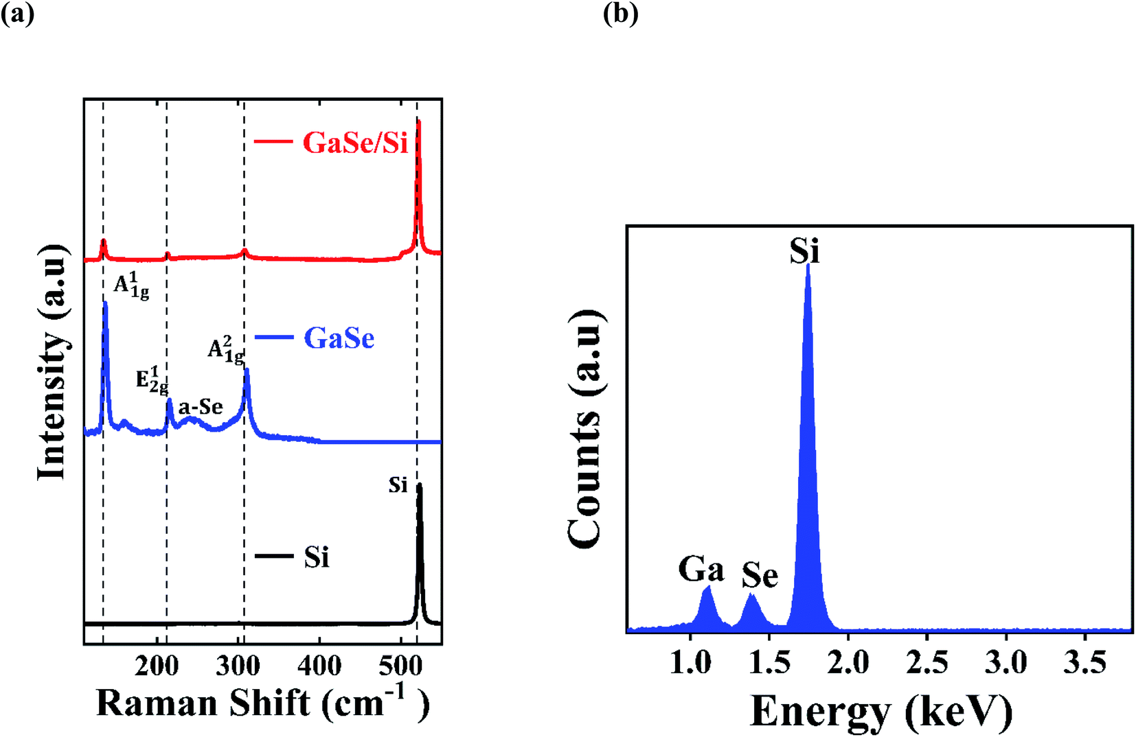 | ||
| Fig. 3 (a) Raman spectra of isolated Si, GaSe, and their overlapped region. (b) EDS spectrum of the GaSe/Si p–n heterojunction. | ||
Before carrying out the photodetection measurements on the GaSe/Si vertical p–n heterojunction, the current–voltage (I–V) characteristics of the heterostructure were examined in dark conditions at room temperature. The I–V curve from the heterostructure in Fig. 4c shows a very clear diode-like nature with a high current rectification ratio. Prior to the fabrication of the heterostructure, we conducted a separate study on the ohmic contact formations on n-Si and p-GaSe. Eutectic In–Ga provided perfect ohmic behavior on n-Si, and nearly ohmic behavior was observed in the case of p-GaSe with Ti(30 nm)/Au(60 nm) as metal contacts. The linear I–V characteristics on p-GaSe are shown in Fig. 4a and those for n-Si are shown in Fig. 4b. The lower dark current drawn from the p-GaSe, as compared to the n-Si, is attributed to the lower hall mobility and higher resistivity of the p-type GaSe layered structure than of the bulk n-Si.45 Since both the p-GaSe and n-Si provide a linear I–V relationship, we can conclude that the nonlinear rectifying nature of the I–V curve from the GaSe/Si p–n heterojunction in Fig. 4c must originate from the GaSe/Si heterojunction itself. The semi-log plot of the same I–V characteristics is shown in the inset of Fig. 4c. The device presents a very good rectifying characteristic, with a high forward current of nearly 100 μA at +5 V and a low-leakage current of nearly 0.1 μA at −5 V, offering a high current rectification ratio of nearly 1000.
 | ||
| Fig. 4 I–V measurements on (a) p-GaSe and (b) n-Si in dark conditions using the Ti/Au and In–Ga eutectic electrodes, respectively. The insets present the schematics of the arrangements for carrying out the I–V measurements. (c) I–V characteristics of the p-GaSe/n-Si heterojunction diode under dark conditions at room temperature, showing a clear current rectification. | ||
The I–V characteristics of this vertical GaSe/Si heterojunction under dark conditions could be described by the thermionic emission model, given by eqn (1), which takes into account the current transport of majority charge carriers from the GaSe film to Si.46
 | (1) |
Moreover, the values of the ideality factor, η, and the barrier height, φ, can be evaluated with the help of the following equations:
 | (2) |
 | (3) |
 | (4) |
Based on the above equations, the values of the ideality factor and the barrier height have been estimated to be approximately 4.9 and 439 meV, respectively. This large ideality factor is attributed to the presence of interface states at the GaSe/Si junction. Since the p–n heterojunction diode has been fabricated via mechanical exfoliation with the help of scotch tape, the interface between Si and GaSe is not free from these interface states. As a result, the mechanism of carrier transport is no longer followed solely by thermionic emission, but some additional transport mechanisms such as recombination and tunneling become dominant, thereby increasing the value of the ideality factor. This large ideality factor value was also reported previously by several groups.20,31
To study the photoresponse behavior of the as-fabricated p–n heterojunction diode, it was irradiated with a monochromatic light of wavelength 580 nm (energy: 2.1 eV, greater than the bandgap of GaSe). The light was vertically incident on the GaSe/Si heterostructure device, and the corresponding photo-generated current was patterned. A significant increment in current was seen compared to the dark current, which is clearly visible in Fig. 5a. The incident light generates adequate electron–hole pairs in the junction, which are promptly separated by the existing electric field, originating from the applied bias, and it contributes to the enhancement in current. A strong photoresponse was also observed even at zero bias, which clearly indicates the existence of a built-in potential in the heterojunction, thereby making it a promising candidate for self-powered photodetectors. To further investigate the photoresponsive effect at the GaSe/Si heterojunction, it was subjected to laser light of varying power densities ranging from 40.7 mW cm−2 to 44.6 mW cm−2, keeping the wavelength fixed at 580 nm, as illustrated in Fig. 5b. It was found that at an applied bias of −5 V and a fixed power density of 44.6 mW cm−2, the current in the p–n heterostructure device increases from −1.45 × 10⁻⁷ A to −3.21 × 10⁻⁵ A, which gives a photo-to-dark-current-ratio of about 221. In the reverse bias condition, the depletion width of the heterojunction increases, which results in significant enhancement of the electric field at the junction. The strong electric field decreases the carrier transit time, leading to reduced carrier recombination. Therefore, the large number of electron–hole pairs produced at the junction can be separated sufficiently and promptly, which is manifested as photocurrent. Upon increasing the power density of the incident illumination, a larger number of photo-generated charge carriers are available at the junction, thereby increasing the photocurrent to a greater extent. In contrast, under the forward bias condition, there exists a negligible depletion layer at the heterojunction, and hence the number of photo-generated charge carriers is relatively small as compared to the forward bias current. Therefore, because of the lack of availability of the photo-generated charge carriers in the forward bias, the photocurrent does not significantly increase the way it increases in the reverse bias condition upon increasing the incident power, as shown in Fig. 5b. A similar observation was reported by Lv et al.16 for their photodetector based on a graphene sandwiched GaSe/WS2 heterojunction. Shin et al.26 found a similar trend for their MoS2/Si vertical heterojunction photodetector.
 | ||
| Fig. 5 Semilog plot of the current–voltage characteristics of the as-fabricated device under (a) dark and illumination conditions (using a 580 nm laser with a power density of 46.9 mW cm−2), and (b) a fixed 580 nm laser light illumination with variable power densities. (c) The plots of the responsivity and specific detectivity with varying power densities. The inset shows the magnified plots of the same, highlighting the values of responsivity and specific detectivity at the lowest power density of 40.7 mW cm−2. (d) Variation of responsivity with applied bias voltage. The inset demonstrates the magnified plot of the responsivity vs. the applied bias curve near the zero bias voltage. | ||
The performance of the heterojunction photodetector was evaluated based on figure of merit parameters such as the photoresponsivity (Rλ), noise equivalent power (NEP), specific detectivity (D*), and external quantum efficiency (EQE). Photoresponsivity quantifies the response of a photodetector when a photon is incident on it, which is calculated as the amount of photocurrent per unit incident power on the effective area of the device. It is mathematically represented by:
 | (5) |
The specific detectivity gives a measure of the ability of a photodetector to distinguish weak optical signals from noise, and it is expressed as:
 | (6) |
 , represents the NEP, which expresses the minimum power detectable per square root bandwidth of a photodetector. The EQE measures the photon-to-electron conversion efficiency, and it is given by the following equation:
 | (7) |
By using eqn (5) and (6), the variations of the photoresponsivity and the specific detectivity of the p–n heterojunction photodetector with power density were studied, which has been illustrated in Fig. 5c. As can be seen from Fig. 5c, there is a continuous rise in the values of both the photoresponsivity and specific detectivity with the power density of the incident illumination. The photocurrent increases significantly with the increasing power density, leading to high values of Rλ and D. For the present device, the effective device area is approximately 22 μm2. At a biasing of −5 V, with a 580 nm laser light of power density of 44.6 mW cm−2, the D and Rλ values of the photodetector have been evaluated to be ∼6.2 × 10¹² Jones (1 Jones = 1 cm  W−1) and ∼2.8 × 10³ A W−1, respectively. The inset of Fig. 5c shows that under the minimum light illumination of 40.7 mW cm−2, both the responsivity and detectivity have significant values of approximately 25 A W−1 and 4.4 × 10¹⁰ Jones, respectively. These high values of Rλ and D point out that the GaSe/Si based photodetector is very sensitive to incident weak optical signals. The variation of Rλ with applied bias voltage was also studied, and it is plotted in Fig. 5d. As can be observed from Fig. 5d, Rλ increases with increasing bias voltage, and the inset of Fig. 5d clearly indicates that the device has an excellent photoresponsivity of 6 A W−1 even at zero bias. Under the zero bias, the electron–hole pairs generated from the incident illumination are swept in the opposite directions with the help of the built-in electric field present at the p–n heterojunction, giving a non-zero value of photoresponsivity; thus, the device is self-powered. Moreover, for the fabricated GaSe/Si p–n heterostructure, at a biasing of −5 V, the NEP value has been extracted to be 2.0 × 10⁻¹³ A Hz−1/2. Also, the EQE value was calculated by using eqn (7), and a high value of ∼6011 was obtained at a biasing of −5 V, which is very promising in the field of photodetection. A comparative study of the key parameters of a photodetector for our fabricated GaSe/Si p–n heterojunction device was carried out and is summarized in Table 1.
| Devices | Measurement conditions | Responsivity (A W−1) | Specific detectivity (Jones) | EQE | Response time | Reference |
|---|---|---|---|---|---|---|
| MoS2/Si | λ = 365 nm | 7.2 | ∼109 | ∼25 | N.A. | 30 |
| V = −2 V | ||||||
| GaSe/MoS2 | λ = 532 nm | 0.35 | ∼1010 | 0.82 | 50 ms | 47 |
| V = 2 V | ||||||
| WSe2/GaSe | λ = 520 nm | 6.2 | ∼1010 | ∼15 | 30 μs | 48 |
| V = −1.5 V | ||||||
| GaSe/WS2 | λ = 410 nm | 149 | 4.3 × 10¹² | ∼450 | 37 μs | 16 |
| V = 2 V | ||||||
| GaSe/InSe | λ = 410 nm | 350 | 3.7 × 10¹² | ∼1060 | 2 μs | 15 |
| V = 2 V | ||||||
| GaSe/MoS2 | λ = 520 nm | 0.67 | 2.3 × 10¹¹ | 1.6 | 155 μs | 49 |
| V = 0 V | ||||||
| WS2/Si | λ = 630 nm | 1.15 | ∼1011 | 1.16 | 42 ms | 50 |
| V = −1 V | ||||||
| GaSe/Si | λ = 580 nm, | 6 | 7.2 × 10¹⁰ | 12.85 | 1.4 s | This work |
| V = 0 V | ||||||
| λ = 580 nm | 2.8 × 10³ | 6.2 × 10¹² | 6011 | |||
| V = −5 V |
The excellent photoelectrical performance of our fabricated GaSe/Si-based 2D/3D vertical heterostructure device can be attributed to the following factors:
(i) The vertical structure of the device reduces the transport channel length of the photogenerated charge carriers, which reduces the probability of recombination and thereby effectively enhances the carrier collection efficiency.
(ii) The type-II band alignment and the presence of the built-in potential at the GaSe/Si p–n heterostructure aid efficient separation of the photogenerated charge carriers, leading to an increased lifetime of the photogenerated electron–hole pairs.
(iii) Generally, photodetectors exploiting the photovoltaic effect have poor responsivity due to the lack of internal gain.51 However, in this case, a photo-multiplication52 (PM) process comes into play when the heterojunction is illuminated with laser light under an applied bias. Trap states exist in GaSe and at the interface between GaSe and Si.53 These trap states prolong the lifetime of the photo-generated charge carriers so that the carriers can cycle the GaSe channel many times before recombination with the help of external bias.
In brief, the large electric field and the short transit time at the vertical 2D/3D heterojunction contribute significantly to increasing the photocurrent, which is directly manifested as high photoconductive gain, specific detectivity, and EQE, demonstrating its great potential towards future optoelectronic applications.
The temporal response of the GaSe/Si vertical p–n heterojunction device was also recorded with the help of a 580 nm laser light, having a power density of 44.6 mW cm−2 at a constant bias voltage of −5 V. The laser light was illuminated on the device periodically by switching the laser between the on and off states with an interval of 10 seconds. As can be seen from Fig. 6a, the photocurrent increases sharply on the left edge of every pulse. This happens because of the sudden rise in photogenerated charge carriers upon illumination. Later, the photocurrent increases slowly and finally attains a constant value. A similar behavior is observed in the photocurrent when the laser light is switched off. Fig. 6b represents the magnified plot of one cycle, and it shows that the GaSe/Si p–n heterojunction-based photodetector has an approximate rise time of 1.4 seconds and decay time of 1.3 seconds. It is worthwhile to mention that the temporal response of the device was recorded by manual switching of the laser light without using any chopper. The slow response of the device can be accredited to the trap states present at the p–n heterojunction interface. Moreover, the GaSe flakes were mechanically exfoliated, and it has been reported that flakes obtained by mechanical exfoliation are prone to edge defects, which serve as traps to the photogenerated electron–hole pairs and reduce the overall speed of the fabricated device.36,54,55
 | ||
| Fig. 6 (a) Temporal response of the GaSe/Si p–n heterojunction device, observed under the illumination of a laser light with a wavelength of 580 nm and power density of 44.6 mW cm−2, at −5 V biasing. (b) Magnified curve of one response cycle. | ||
We further carried out KPFM measurements on the vertical GaSe/Si p–n heterostructure to understand its band alignment. KPFM is one of the electrical modes of AFM; it is used to obtain workfunction values and information regarding the surface potential and charge at the nanoscale.56 A few research groups previously utilized this technique to examine the alignment of bands at the 2D/3D interface.20,30 KPFM basically measures the contact potential difference (CPD) between a conducting AFM tip and a sample surface by reading long-range electrostatic forces generated from the probe–sample interactions. In our present work, this technique was utilized to estimate the conduction band offset value at the GaSe/Si heterostructure. Fig. 7a portrays the surface potential mapping of the vertical GaSe/Si heterostructure, and Fig. 7b plots the variation of surface potential with respect to lateral distance at the GaSe/Si site along the dashed line as highlighted in Fig. 7a. The CPD between the sample substrate and the tip is defined as:
 | (8) |
 | ||
| Fig. 7 (a) Kelvin probe force microscopy (KPFM) image of the GaSe flake on Si substrate, indicating the change in surface potential between GaSe and Si. (b) Variation of surface potential with position across the GaSe/Si heterojunction along the dashed line depicted in (a). | ||
The change in CPD values between GaSe and Si is given by
 | (9) |
In Fig. 7b, this change in CPD between GaSe and Si at the GaSe/Si interface can be seen clearly. The surface potential value of the Si sample is 146 mV greater than that of the GaSe film. Therefore, the difference in work function values between Si and GaSe is evaluated as:
| ∅Si − ∅GaSe ≈ 146 meV | (10) |
This result, obtained from the KPFM measurement, gives direct proof of the junction formation between the GaSe flake and the Si substrate.
Next, to obtain the conduction band offset value for the heterojunction, we can use the following set of equations:
Considering the bandgap of GaSe as 2 eV,57 we have
| EGaSeC − EGaSeV = 2.0 eV | (11) |
Also, we know from the semiconductor fundamentals58 that
 | (12) |
Subtracting eqn (12) from (11), we have
 | (13) |
Also,
 | (14) |
| EGaSeC − EGaSeF = 1.714 eV | (15) |
| ESiC − ESiF = 0.205 eV | (16) |
Subtracting eqn (16) from eqn (15), we can find the value of the conduction band offset, ΔEC, which is given by
| ΔEC = EGaSeC − ESiC = (EGaSeF − ESiF) + 1.714 − 0.205 | (17) |
Therefore,
| ΔEC = 1.509 − (ESiF − EGaSeF) = 1.509 − (∅Si − ∅GaSe) | (18) |
The value of the workfunction difference, (∅Si − ∅GaSe), was experimentally found from KPFM measurements, as given in eqn (10). Thus, the conduction band offset value was calculated to be 1.36 eV.
As per Anderson's rule,60 the difference in electron affinity values between GaSe and Si provides the conduction band offset, ΔEC.
| ΔEC = χSi − χGaSe | (19) |
The reported values of χSi and χGaSe are 4.1 eV and 2.7 eV, respectively,61 which gives the value of ΔEC to be 1.4 eV. This value is in good agreement with our experimentally obtained result.
Further, the depletion width was estimated using the value of the built-in potential (Vbi), and finally, the energy band diagram was drawn. The energy band diagram, shown in Fig. 8a–d, helps to understand the current transport in the GaSe/Si p–n heterojunction.
 | ||
| Fig. 8 Band alignment at the vertical 2D/3D GaSe/Si heterojunction interface. (a) Band alignment for isolated GaSe and Si. The conduction band offset, ΔEC, has a value of ∼1.4 eV. (b–d) Band alignment at the GaSe/Si p–n heterojunction interface at different applied biases: (b) zero bias, (c) reverse bias, and (d) forward bias. | ||
Ideally, the work function difference between GaSe and Si provides the built-in potential barrier.
| eVbi = ∅Si − ∅GaSe ≈ 146 meV as measured by KPFM | (20) |
The depletion width is given by
 | (21) |
Moreover, the built-in potential (Vbi) values can be evaluated on both sides using the following equations:
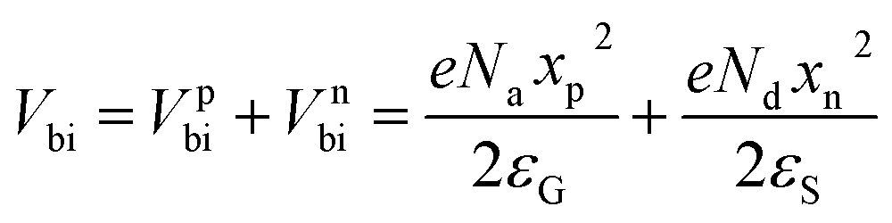 | (22) |
| Vpbi = 144.7 mV and Vnbi = 0.74 mV | (23) |
Therefore, the built-in potential barriers in the GaSe and Si sides were evaluated to be 144.7 mV and 0.75 mV, respectively. These values of the built-in potential and the depletion width are used to evolve the band diagram and charge transport.
To understand the current transport and photoelectrical behavior of the heterostructure device, a schematic energy band diagram, based on the type-II band alignment, has been drawn in Fig. 8. A conduction band offset value of approximately 1.4 eV exists in the heterojunction, as depicted in Fig. 8a. Under the zero bias condition, the Fermi levels of Si and GaSe become aligned, which causes band bending at the junction (Fig. 8b). Upon illumination, the photogenerated electron–hole pairs are collected by the electrodes with the help of the built-in potential present at the heterojunction, giving a non-zero photoresponsivity even at zero bias; thus, the device is self-powered. In Fig. 8c, when the heterostructure device is given negative biasing, a strong electric field is developed at the GaSe/Si heterojunction; as a result, the carrier transit time is shortened, which in turn reduces the carrier recombination. Thus, an excellent photoresponse is observed under this condition. Under the forward bias condition, as shown in Fig. 8d, the barrier height at the interface is reduced and a large amount of current flows through the junction.
Conclusions
In this work, we have fabricated a vertical 2D/3D p–n heterojunction photodetector using mechanically exfoliated p-GaSe and n-type Si. The KPFM measurements on the device show that a type-II band alignment exists at the GaSe/Si heterojunction. Surface potential mapping at the heterojunction was carried out to extract the conduction band offset value, which was found to be ∼1.4 eV. The current–voltage measurements on the device reveal that the GaSe/Si photodiode exhibits a rectifying nature, with a high current rectification ratio of approximately 1000 at ±5 V. The photoresponse measurement on the fabricated device shows excellent performance, with high photoresponsivity, specific detectivity, and EQE values of ∼2.8 × 10³ A W−1, 6.2 × 10¹² Jones, and 6011, respectively, at a biasing of −5 V. Moreover, an excellent photoresponse of 6 A W−1, obtained at the zero bias, suggests that the heterojunction device does not require any external power to operate. These results show the promising potential of self-driven GaSe/Si-based 2D/3D heterostructure devices in the field of photodetection. This work may pave the way to designing innovative optoelectronic devices by integrating low-dimensional materials with conventional 3D semiconducting materials.Author contributions
Sahin Sorifi: validation, formal analysis, investigation, data curation, visualization, writing – original draft. Shuchi Kaushik: methodology. Rajendra Singh: conceptualization, writing – review & editing, supervision, funding acquisition.Conflicts of interest
There are no conflicts to declare.Acknowledgements
The authors acknowledge the Nanoscale Research Facility (NRF), Indian Institute of Technology Delhi for providing device fabrication and characterization facilities. Sahin Sorifi would like to thank the Department of Science and Technology (DST), India for supporting with a research fellowship. The authors would also like to acknowledge the ‘Grand Challenge Project on MBE growth of 2D materials’ sponsored by the Ministry of Human Resource Development (MHRD), India, and the Indian Institute of Technology Delhi for partial financial support for this work.References
- Y. Xu, Z. Wang, Z. Guo, H. Huang, Q. Xiao, H. Zhang and X.-F. Yu, Adv. Opt. Mater., 2016, 4, 1223–1229 CrossRef CAS.
- J. Li and G. Zheng, Adv. Sci., 2017, 4, 1600380 CrossRef PubMed.
- O. Lopez-Sanchez, D. Lembke, M. Kayci, A. Radenovic and A. Kis, Nat. Nanotechnol., 2013, 8, 497–501 CrossRef CAS PubMed.
- S. H. Park, R. Su, J. Jeong, S.-Z. Guo, K. Qiu, D. Joung, F. Meng and M. C. McAlpine, Adv. Mater., 2018, 30, 1803980 CrossRef PubMed.
- K. S. Novoselov, D. Jiang, F. Schedin, T. J. Booth, V. V. Khotkevich, S. V. Morozov and A. K. Geim, Proc. Natl. Acad. Sci., 2005, 102, 10451–10453 CrossRef CAS PubMed.
- R. Ganatra and Q. Zhang, ACS Nano, 2014, 8, 4074–4099 CrossRef CAS PubMed.
- J. D. Yao, Z. Q. Zheng, J. M. Shao and G. W. Yang, Nanoscale, 2015, 7, 14974–14981 RSC.
- H. Huang, P. Wang, Y. Gao, X. Wang, T. Lin, J. Wang, L. Liao, J. Sun, X. Meng, Z. Huang, X. Chen and J. Chu, Appl. Phys. Lett., 2015, 107, 143112 CrossRef.
- S. Z. Butler, S. M. Hollen, L. Cao, Y. Cui, J. A. Gupta, H. R. Gutiérrez, T. F. Heinz, S. S. Hong, J. Huang, A. F. Ismach, E. Johnston-Halperin, M. Kuno, V. V. Plashnitsa, R. D. Robinson, R. S. Ruoff, S. Salahuddin, J. Shan, L. Shi, M. G. Spencer, M. Terrones, W. Windl and J. E. Goldberger, ACS Nano, 2013, 7, 2898–2926 CrossRef CAS.
- F. Xia, H. Wang, D. Xiao, M. Dubey and A. Ramasubramaniam, Nat. Photonics, 2014, 8, 899–907 CrossRef CAS.
- L. Britnell, R. V. Gorbachev, R. Jalil, B. D. Belle, F. Schedin, A. Mishchenko, T. Georgiou, M. I. Katsnelson, L. Eaves, S. V. Morozov, N. M. R. Peres, J. Leist, A. K. Geim, K. S. Novoselov and L. A. Ponomarenko, Science, 2012, 335, 947–950 CrossRef CAS PubMed.
- X. Zhou, X. Hu, J. Yu, S. Liu, Z. Shu, Q. Zhang, H. Li, Y. Ma, H. Xu and T. Zhai, Adv. Funct. Mater., 2018, 28, 1706587 CrossRef.
- S. Kaushik and R. Singh, Adv. Opt. Mater., 2021, 2002214 CrossRef CAS.
- N. Zhou, R. Wang, X. Zhou, H. Song, X. Xiong, Y. Ding, J. Lü, L. Gan and T. Zhai, Small, 2018, 14, 1702731 CrossRef PubMed.
- F. Yan, L. Zhao, A. Patanè, P. Hu, X. Wei, W. Luo, D. Zhang, Q. Lv, Q. Feng, C. Shen, K. Chang, L. Eaves and K. Wang, Nanotechnology, 2017, 28, 27LT01 CrossRef.
- Q. Lv, F. Yan, X. Wei and K. Wang, Adv. Opt. Mater., 2018, 6, 1700490 CrossRef.
- W. Wei, Y. Dai, C. Niu, X. Li, Y. Ma and B. Huang, J. Mater. Chem. C, 2015, 3, 11548–11554 RSC.
- C. K. Zankat, P. M. Pataniya, A. Patel, S. A. Bhakhar, S. Narayan, G. K. Solanki, K. D. Patel, V. M. Pathak, C. K. Sumesh and P. K. Jha, Mater. Today Energy, 2020, 18, 1–9 Search PubMed.
- X. Li, M. W. Lin, J. Lin, B. Huang, A. A. Puretzky, C. Ma, K. Wang, W. Zhou, S. T. Antelides, M. Hi, I. Kravchenko, J. Fowlkes, C. M. Ouleau, D. B. Geohegan and K. Xiao, Sci. Adv., 2016, 2(4) DOI:10.1126/sciadv.1501882.
- D. Ruzmetov, K. Zhang, G. Stan, B. Kalanyan, G. R. Bhimanapati, S. M. Eichfeld, R. A. Burke, P. B. Shah, T. P. O'Regan, F. J. Crowne, A. G. Birdwell, J. A. Robinson, A. V. Davydov and T. G. Ivanov, ACS Nano, 2016, 10, 3580–3588 CrossRef CAS PubMed.
- F. Wang, K. Pei, Y. Li, H. Li and T. Zhai, Adv. Mater., 2021, 33, 2005303 CrossRef CAS.
- Y. Liu, M. Chen and S. Yang, InfoMat, 2021, 3, 231–251 CrossRef CAS.
- Z. Li, D. Li, H. Wang, P. Chen, L. Pi, X. Zhou and T. Zhai, Small Methods, 2021, 5, 2100567 CrossRef PubMed.
- E. W. Lee, L. Ma, D. N. Nath, C. H. Lee, A. Arehart, Y. Wu and S. Rajan, Appl. Phys. Lett., 2014, 105, 203504 CrossRef.
- E. W. Lee, C. H. Lee, P. K. Paul, L. Ma, W. D. McCulloch, S. Krishnamoorthy, Y. Wu, A. R. Arehart and S. Rajan, Appl. Phys. Lett., 2015, 107, 103505 CrossRef.
- G. H. Shin, J. Park, K. J. Lee, G.-B. Lee, H. B. Jeon, Y.-K. Choi, K. Yu and S.-Y. Choi, ACS Appl. Mater. Interfaces, 2019, 11, 7626–7634 CrossRef CAS.
- L. Wang, J. Jie, Z. Shao, Q. Zhang, X. Zhang, Y. Wang, Z. Sun and S.-T. Lee, Adv. Funct. Mater., 2015, 25, 2910–2919 CrossRef CAS.
- A. Ur Rehman, M. F. Khan, M. A. Shehzad, S. Hussain, M. F. Bhopal, S. H. Lee, J. Eom, Y. Seo, J. Jung and S. H. Lee, ACS Appl. Mater. Interfaces, 2016, 8, 29383–29390 CrossRef PubMed.
- M.-L. Tsai, S. Su, J. Chang, D. Tsai, C.-H. Chen, C. Wu, L. Li, L. Chen and J. He, ACS Nano, 2014, 8, 8317–8322 CrossRef CAS.
- Y. Li, C.-Y. Xu, J.-Y. Wang and L. Zhen, Sci. Rep., 2015, 4, 7186 CrossRef.
- M. Moun, M. Kumar, M. Garg, R. Pathak and R. Singh, Sci. Rep., 2018, 8, 11799 CrossRef PubMed.
- T. Cui, R. Lv, Z.-H. Huang, S. Chen, Z. Zhang, X. Gan, Y. Jia, X. Li, K. Wang, D. Wu and F. Kang, J. Mater. Chem. A, 2013, 1, 5736 RSC.
- V. Dhyani and S. Das, Sci. Rep., 2017, 7, 44243 CrossRef PubMed.
- J. Li, X. Xi, S. Lin, Z. Ma, X. Li and L. Zhao, ACS Appl. Mater. Interfaces, 2020, 12, 11965–11971 CrossRef CAS PubMed.
- C. Liu, X. Li, T. Hu, W. Zhu, F. Yan, T. Wu, K. Wang and L. Zhao, Nanoscale, 2021, 13(41), 17512–17520 RSC.
- P. Hu, Z. Wen, L. Wang, P. Tan and K. Xiao, ACS Nano, 2012, 6, 5988–5994 CrossRef CAS PubMed.
- H. Huang, P. Wang, Y. Gao, X. Wang, T. Lin, J. Wang, L. Liao, J. Sun, X. Meng, Z. Huang, X. Chen and J. Chu, Appl. Phys. Lett., 2015, 107, 143112 CrossRef.
- F. Yan, C. Hu, Z. Wang, H. Lin and K. Wang, Appl. Phys. Lett., 2021, 118, 190501 CrossRef CAS.
- X. Wang, X. Zhao, C. Hu, Y. Zhang, B. Song, L. Zhang, W. Liu, Z. Lv, Y. Zhang, J. Tang, Y. Sui and B. Song, Appl. Phys. Lett., 2016, 109, 023502 CrossRef.
- W. Luo, Y. Cao, P. Hu, K. Cai, Q. Feng, F. Yan, T. Yan, X. Zhang and K. Wang, Adv. Opt. Mater., 2015, 3, 1418–1423 CrossRef CAS.
- D. V. Rybkovskiy, N. R. Arutyunyan, A. S. Orekhov, I. A. Gromchenko, I. V. Vorobiev, A. V. Osadchy, E. Y. Salaev, T. K. Baykara, K. R. Allakhverdiev and E. D. Obraztsova, Phys. Rev. B: Condens. Matter Mater. Phys., 2011, 84, 085314 CrossRef.
- A. Kuhn, A. Chevy and R. Chevalier, Phys. Status Solidi A, 1975, 31, 469–475 CrossRef CAS.
- P. J. Carroll and J. S. Lannin, Solid State Commun., 1981, 40, 81–84 CrossRef CAS.
- M.-H. Doan, Y. Jin, S. Adhikari, S. Lee, J. Zhao, S. C. Lim and Y. H. Lee, ACS Nano, 2017, 11, 3832–3840 CrossRef CAS PubMed.
- V. Augelli, C. Manfredotti, R. Murri and L. Vasanelli, Phys. Rev. B: Condens. Matter Mater. Phys., 1978, 17, 3221–3226 CrossRef CAS.
- L. Zeng, C. Xie, L. Tao, H. Long, C. Tang, Y. H. Tsang and J. Jie, Opt. Express, 2015, 23, 4839 CrossRef CAS.
- A. Islam, J. Lee and P. X. L. Feng, ACS Photonics, 2018, 5, 2693–2700 CrossRef CAS.
- X. Wei, F. Yan, Q. Lv, C. Shen and K. Wang, Nanoscale, 2017, 9, 8388–8392 RSC.
- Z. He, J. Guo, S. Li, Z. Lei, L. Lin, Y. Ke, W. Jie, T. Gong, Y. Lin, T. Cheng, W. Huang and X. Zhang, Adv. Mater. Interfaces, 2020, 7, 1901848 CrossRef CAS.
- R. K. Chowdhury, R. Maiti, A. Ghorai, A. Midya and S. K. Ray, Nanoscale, 2016, 8, 13429–13436 RSC.
- M. Buscema, J. O. Island, D. J. Groenendijk, S. I. Blanter, G. A. Steele, H. S. J. van der Zant and A. Castellanos-Gomez, Chem. Soc. Rev., 2015, 44, 3691–3718 RSC.
- L. Li, F. Zhang, W. Wang, Q. An, J. Wang, Q. Sun and M. Zhang, ACS Appl. Mater. Interfaces, 2015, 7, 5890–5897 CrossRef CAS.
- S. Ghatak, A. N. Pal and A. Ghosh, ACS Nano, 2011, 5, 7707–7712 CrossRef CAS.
- S. Kaushik, S. Sorifi and R. Singh, Photonics Nanostructures - Fundam. Appl., 2021, 43, 100887 CrossRef.
- S. Kaushik, T. R. Naik, M. Ravikanth, C.-H. Liao, X. Li, V. R. Rao and R. Singh, Semicond. Sci. Technol., 2021, 36, 055001 CrossRef CAS.
- M. Nonnenmacher, M. P. O'Boyle and H. K. Wickramasinghe, Appl. Phys. Lett., 1991, 58, 2921–2923 CrossRef.
- S. Sorifi, M. Moun, S. Kaushik and R. Singh, ACS Appl. Electron. Mater., 2020, 2, 670–676 CrossRef CAS.
- D. A. Neamen and D. Biswas, Semiconductor Physics and Devices, Mc Graw Hill Education, 4th edn, 2007 Search PubMed.
- V. G. Voevodin, O. V. Voevodina, S. A. Bereznaya, Z. V. Korotchenko, A. N. Morozov, S. Y. Sarkisov, N. C. Fernelius and J. T. Goldstein, Opt. Mater., 2004, 26, 495–499 CrossRef CAS.
- R. L. Anderson, IBM J. Res. Dev., 1960, 4, 283–287 CAS.
- P. J. Ko, A. Abderrahmane, T. Takamura, N.-H. Kim and A. Sandhu, Nanotechnology, 2016, 27, 325202 CrossRef PubMed.
| This journal is © The Royal Society of Chemistry 2022 |