DOI:
10.1039/D1NA00321F
(Paper)
Nanoscale Adv., 2022,
4, 1464-1482
A DFT study of SenTen clusters†
Received
3rd May 2021
, Accepted 14th January 2022
First published on 15th January 2022
Abstract
First principles calculations have been performed to study the characteristic properties of SenTen (n = 5–10) clusters. The present study reveals that the properties of these small clusters are consistent with the properties of Se–Te glassy systems. Several hundred equilibrium structures obtained from a genetic algorithm based USPEX code are relaxed to their minimum energy using the VASP code. Most of the lowest energy buckled ring-like structures are formed from Se–Te heteropolar bonds. Detailed structural analysis and distance energy plots unveil that many equilibrium structures are close in energy to their global minimum. The computed Raman and IR spectra show the dominance of Se–Te heteropolar bonds, consistent with earlier simulation and experimental findings in Se1−xTex glass materials. Low frequency vibrational modes observed in small clusters are characteristic features of amorphous materials. Non-bonding orbitals (lone pair) are observed in the HOMO, whereas the LUMO is formed from purely antibonding orbitals. The dielectric functions corroborate the bonding mechanism and slightly polar nature of SenTen clusters. The energy loss and absorption coefficient indicate the presence of π–plasmons in the UV-visible region. Furthermore, it is ascertained that the use of a hybrid functional (B3LYP) does not affect the properties of small clusters appreciably, except causing a blue shift in the optical spectra. Hence, we find that the small clusters have bearing on the formation of glassy Se–Te systems.
1 Introduction
Nanoclusters have received attention because of their unique properties and technological applications. The exceptional structural, electronic, optical, magnetic and catalytic properties1,2 of clusters facilitate their use in nano-solid state devices. They have potential applications in carbon nanotubes, semiconductor nanowires, chemical catalysts, creation of memory cells, lasers and photonics.3 Small clusters are considered as the building blocks of nanomaterials, and hence, play a vital role in determining the properties of these materials. Consequently, cluster-assembled materials are likely to exhibit unique properties.4 Recently, transition metal and semiconductor clusters have been studied5,6 because of their interesting magnetic and optical properties, respectively. Nanostructured transition metal chalcogenides have gained enormous consideration due to their typical chemical stability, electronic properties and remarkable structure.7
Since, clusters exhibit properties of molecule and bulk, hence, they are known as 5th state of matter.8 The computational convenience of clusters makes them a supplement to conventional large systems and thus they are considered as microscopic analogues of bulk systems. Small clusters exhibit size dependent effects not observed in bulk systems. The properties of clusters are expected to converge to their bulk as the cluster size approaches the bulk dimensions. A high value of the ratio of the number of atoms on the surface to that inside the cluster show the properties of a bulk surface without affecting their reactivity. Size dependent effects in small clusters are the origin of the coexistence of liquid-like and solid-like states.9 The size and composition of a cluster can be controlled with atomic precision. Mostly clusters exhibit a large number of isomers, in which atoms are arranged in different configurations/structures. Separation between different structures, i.e., ordered and disordered structures, has been discussed in several ways.10 Disordered structures are said to exhibit amorphous nature.10,11 The concept of amorphous or glassy clusters was reported by Rose and Berry.10 According to them, if a cluster has a large number of inherent disorder structures compared to ordered structures, it can be considered to have a microamorphous (MA) state. The MA state is a small analogue to the bulk, in reference to the properties of bulk glass. For a MA state to exist, clusters must be trappable into solid amorphous structures through realistic experimental processes. The existence of disorder structures as a low energy configuration has been reported12–15 in the literature. Bulgac and co-workers have reported the existence of small Na8 glassy clusters.16 The literature shows the existence of many more glassy clusters9,10,17
Most of the surface properties are determined by the nanostructures present on the surface. The formation, growth and dynamics of surfaces are believed to be essential components in device fabrication.18 Researchers have focused on the use of free clusters for assembling nano-structured thin films.1 Nanostructured films obtained by assembling atomic clusters are of strategic importance for a wide variety of applications.1,2 Recently, nano-structured thin films were prepared and their structural, optical and electrical properties were studied.19–23 The formation of small clusters has been noticed23 in Se–Te thin films. The presence of small structures or defects in thin films has a significant impact on their structural and functional properties.24,25 The synthesis, characterization and different properties of Se–Te nanostructured thin films26,27 have been reported in the literature. Amorphous nano-structured Se–Te films have shown enhanced and direct band gaps not reported for their counterparts,28,29 crystals. The Raman spectra and photoluminescence study of Te94Se6 nanoparticles thin films have shown their application in optical disk and semiconducting devices.28 Tripathi et al.30 have reported the optical properties of nanostructured selenium-tellurium thin films grown by a thermal evaporation technique. Several researchers31–33 have reported the electrical and transport properties of chalcogenide glasses. A structural study of Se–Te glasses using Raman spectroscopy and first principles methods has been recently reported34 by A. Tverjanovich et al. They have simulated open triatomic Se–Te clusters and oligomers of Te to compare their results with experiments. Experimental studies35,36 on Se–Te glasses indicate the presence of chain like structures with a significant contribution of Sen and Ten fragments. The Raman study34–36 of Se–Te glasses and triatomic clusters has shown that the Se and Te atoms are randomly distributed in the chain with preference to heteropolar bonds. In view of the isoelectronic nature of Se and Te, it is expected37 that Te not only enters the chain and rings of Se but also favours the cross linking of rings and chains. The addition of Te to Se results in an increase in structural and compositional disorder.
However, studies on nano-chalcogenides are at the primary stage and the overall features are not explored. The study of nano-chalcogenides is crucial for device fabrication. Free from bonding restrictions, amorphous nanostructures may result in a large range of nanostructures, in contrast to crystalline nano-structures. Control on the nanometer scale in nanostructures could be an important area of research in amorphous semiconductors. Thus, the study of nano-chalcogenides is inevitable for their use in nano-devices2 like nano-electronic devices, memory devices, optical memory devices, nanophotonic devices, etc. Furthermore, the increasing focus on free cluster assembled thin films demands the study of small clusters. Clusters of S, Se and Te have been synthesized in experiments like gas condensation and laser vaporization in a pulsed-nozzle cluster source. Detailed discussion on Se–Te small structures is still missing. Here, a first principles study of SenTen clusters will help us to understand the molecular origin of the vitreous state of a material. In this way, the present investigation is an attempt to study the properties of a conventional large system through its microscopic analogue. In the present work, we aim to study the structural, electronic and optical properties of SenTen clusters using the first principles method. SenTen small clusters of different sizes are obtained using the USPEX code.38,39 Most of the buckled ring-like structures exhibit properties similar to the properties of Se–Te glass. Hence, our work is relevant to the experimental work on bulk systems, because bulk as well as Se–Te thin films in their properties show the dominance of small clusters.
2 Computational details
First principles calculations are performed, using the Vienna ab initio simulation code (VASP),40–42 to examine the structural and optical properties of SenTen clusters. The Perdew–Burke–Ernzerhof (PBE) form of the exchange correlation functional of the generalized gradient approximation (GGA) has been employed43,44 to perform the simulations. Projected augmented wave (PAW) pseudo-potentials are used to describe the electron–ion interactions. The outermost valence electrons 4s24p4 of the Se atom and the 5s25p4 valence electrons of the Te atom are considered to compute the potential. Initially, SenTen clusters are generated using the universal structure prediction evolutionary xtallography (USPEX) code.38,39 It generates several hundred possible structures along with their symmetries, knowing only the chemical composition of the system. Only a few (50–60) stable structures of each cluster have been considered for examination. Generated clusters are placed at the center of cubic supercells of different sizes, ranging from 15 to 30 Å depending upon the size of the cluster, so that the interaction among the periodic images of clusters separated by vacuum is negligible. The structural optimization of each cluster is carried out with VASP until all the force components become less than 0.005 eV Å−1 with a convergence of about 10−4 eV Å−1 in the total energy. The USPEX run provides hundreds of structures, but generally many of them are duplicate structures. To isolate the duplicate structures, the Crystal Fingerprint (crystalfp) code45 has been used. The Crystal Fingerprint approach has been further exploited to generate distance energy (DE) plots for these clusters. Established least energy structures (ground state structure) are considered to compute the IR and Raman spectra, eigenvalue value spectrum and optical properties of SenTen clusters.
3 Results and discussion
3.1 Structural and electronic properties
The least energy (ground state) structures of SenTen clusters, n = 5–10, along with a few isomers are presented in Fig. 1 and 2. The energy of the least energy structure is taken as zero and the energy of its isomers is relative. It is observed that SenTen clusters acquire closed chain ring type structures exhibited by pristine Sen and Ten clusters,47 also reported in a Se–Te liquid phase.48 Most of the examined structures are ring type with two nearest neighbours. However, for n = 5, we have noticed a few high energy structures with three nearest neighbours, reported in the ESI (Fig. S1†). SenTen clusters adopt an order–disorder pattern, Fig. 1 and 2, noticed in isolated Sen and Ten clusters.47 The point symmetries, bond lengths, HOMO–LUMO gap and binding energy per atom are given in Table 1. The values given in the table are our results and superscripts a and b on values show that these values are consistent with the values reported in ref. 35 and 46.
 |
| | Fig. 1 Lowest energy isomers of SenTen clusters, n = 5–7. Red spheres represent Te atoms and yellow spheres represent Se atoms. Given energy is in eV. | |
 |
| | Fig. 2 The same as in Fig. 1 for n = 8–10. Given energy is in eV. | |
Table 1 Calculated structural and electronic properties of SenTen clusters
|
n
|
Point sym. |
Bond length (Å) |
H–L gap (eV) |
B.E. per atom (eV) |
| Se–Se |
Te–Te |
Se–Te |
(eV) |
(eV) |
|
Ref. 35.
Ref. 46.
|
| Se5Te5 |
C
5v
|
|
|
2.55a,b |
1.80 |
−3.11 |
|
|
C
s
|
|
|
2.54–2.56a,b |
1.65 |
−3.10 |
|
|
C
1
|
2.39a,b |
2.71a,b |
2.52–2.59a,b |
1.69 |
−3.10 |
|
|
C
s
|
2.36–2.37a,b |
2.73–2.74a,b |
2.55a,b |
1.87 |
−3.09 |
|
|
C
s
|
|
|
2.54–2.57a,b |
1.65 |
−3.09 |
| Se6Te6 |
D
3d
|
|
|
2.55a,b |
1.94 |
−3.11 |
|
|
C
1
|
|
|
2.53–2.58a,b |
1.61 |
−3.11 |
|
|
D
3d
|
|
|
2.55a,b |
1.86 |
−3.11 |
|
|
C
1
|
2.38–2.39a,b |
2.73–2.74a,b |
2.53–2.56a,b |
1.90 |
−3.11 |
|
|
C
1
|
2.35–2.37a,b |
2.74a,b |
2.55a,b |
1.96 |
−3.10 |
| Se7Te7 |
C
s
|
|
|
2.53–2.61a,b |
1.54 |
−3.12 |
|
|
C
s
|
|
|
2.54–2.56a,b |
1.73 |
−3.12 |
|
|
C
1
|
2.36–2.37a,b |
2.67–2.75a,b |
2.51–2.67a,b |
1.48 |
−3.10 |
|
|
C
1
|
2.36–2.39a,b |
2.72–2.76a,b |
2.52–2.57a,b |
1.52 |
−3.10 |
|
|
C
1
|
2.37–2.38a,b |
2.69–2.82a,b |
2.52–2.65 |
1.44 |
−3.09 |
| Se8Te8 |
D
4d
|
|
|
2.55a,b |
1.68 |
−3.12 |
|
|
D
4d
|
|
|
2.55a,b |
1.62 |
−3.108![[thin space (1/6-em)]](https://www.rsc.org/images/entities/char_2009.gif) 9 9 |
|
|
C
1
|
2.37–2.39a,b |
2.71–2.74a,b |
2.53–2.57a,b |
1.65 |
−3.11 |
|
|
C
1
|
2.34–2.41a,b |
2.71–2.77a,b |
2.52–2.59a,b |
1.63 |
−3.11 |
| Se9Te9 |
C
1
|
2.39a,b |
2.69–2.72a,b |
2.52–2.62a,b |
1.53 |
−3.11 |
|
|
C
1
|
2.35–2.36a,b |
2.69–2.73a,b |
2.51–2.62 |
1.62 |
−3.10 |
|
|
C
s
|
2.38–2.40a,b |
2.73–2.74a,b |
2.53–2.56a,b |
1.75 |
−3.10 |
|
|
C
1
|
2.39–2.40a,b |
2.65–2.71a,b |
2.50–2.63 |
1.70 |
−3.10 |
| Se10Te10 |
C
i
|
|
|
2.53–2.58a,b |
1.45 |
−3.12 |
|
|
C
1
|
2.38–2.39a,b |
2.72–2.73a,b |
2.52–2.58a,b |
1.58 |
−3.11 |
|
|
D
5d
|
|
|
2.55a,b |
1.40 |
−3.10 |
|
|
C
2
|
2.37–2.39a,b |
2.73–2.75a,b |
2.54–2.56a,b |
1.55 |
−3.09 |
Binding energy per atom is calculated for each SenTen cluster from the relationship
| |  | (1) |
where
E[Se],
E[Te], and E[Se
nTe
n] represent the energy of an isolated Se atom, Te atom and Se
nTe
n clusters, respectively, and 2
n is the total number of Se and Te atoms in a Se
nTe
n cluster. The dynamic stability of least energy structures is examined from their vibrational frequencies. The computed vibrational frequencies of these structures do not possess any imaginary value, which reveals their dynamic stability. The thermodynamic stability of clusters has been ascertained from mixing energy. The energy of mixing is computed from the equation
49| |  | (2) |
where
N =
m +
n, and
m and
n represent the number of atoms in Se
N and Te
N clusters, respectively. The obtained energy of mixing is reported in
Table 2 along with the B.E per atom of Se
2n and Te
2n clusters. A negative energy of mixing indicates that the alloy formation is thermodynamically favorable.
Table 2 Energy of mixing for Se–Te clusters and BE per atom of Se2n and Te2n clusters
| Cluster |
E
mix (eV) |
B.E. per atom (eV) |
| Te2n |
Se2n |
| Se5Te5 |
−0.40 |
−2.82 |
–3.47 |
| Se6Te6 |
−0.48 |
−2.83 |
–3.47 |
| Se7Te7 |
−0.49 |
−2.84 |
–3.47 |
| Se8Te8 |
−0.72 |
−2.84 |
–3.47 |
| Se9Te9 |
−0.81 |
−2.84 |
–3.46 |
| Se10Te10 |
−0.60 |
−2.83 |
–3.46 |
It is noticed that with an increase in the number of atoms (n), i.e. cluster size, the ring gets buckled and elongated. Though the addition of an atom in a cluster does not change the B.E. per atom much, the geometries get modified, Fig. 1 and 2. The deep examination of these structures reveals that the structural parameters, i.e., bond length and bond angle, do not remain the same throughout the structure, Table 1. All ground state (GS) structures consist of heteropolar Se–Te bonds, except Se9Te9. It has a different geometry consisting of Se–Te, Se–Se and Te–Te bonds. Bonding in these structures shows that Te atoms enter the Se chain and get dissolved in the chain. In some higher energy isomers, the Se–Te–Se–Te–Se bonding pattern is disobeyed and instead, Se–Te–Te–Se, Se–Te–Te–Te–Se, Se–Se–Te–Te–Te–Se, and Se–Te–Te–Te–Te–Se bonding patterns are observed, Fig. 1 and 2. This shows the presence of homopolar bonds along with the heteropolar bonds. The dominance of Se–Te bonds in GS structures is consistent with earlier work,35,46 in the case of open chain structures. Though the bonding arrangements of the isomers are different, the B.E. per atom is very close to the ground state. It differs at the most by 0.35 eV. The bond angle α (x–y–z with x, z = Se/Te and y = Te/Se) has been observed in the range 101° to 111° for all structures. Its value in triatomic clusters34 lies between 105.5° and 108.5°and in Se–Te glasses the reported average bond angle value is 105°.35
To determine the effect of bonding arrangement on ground state structures, we constructed a few structures with 5, 6, 7 and 8 atoms of Se on one side of the ring and of Te on the other side of the ring (not reported here). Structures were relaxed in VASP so as to attain their minimum energy state. It is found that Se and Te atoms do not change their positions, which means that Se–Se and Te–Te homopolar bonds still exist as before relaxation. The B.E. of these relaxed structures is close to the B.E. of the GS structures reported in Fig. 1 and 2. This shows that the B.E per atom of a structure is not affected by the presence of heteropolar/homopolar bonds, a possibility in experiments during film deposition.51
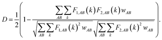
The structural disorder and existence of metastable structures with energy very close to the ground state energy indicate the amorphous nature of SenTen clusters. To complete the structural analysis, we have examined the distance energy (DE) plots, Fig. 3, of SenTen clusters. The DE plot provides necessary information regarding the character of the potential energy surface (PES) and allows us to distinguish between glassy and non-glassy clusters. We have generated the distance energy plots using crystalfp. The fingerprint function (F), which characterizes the structure, is defined as52,53
| |  | (3) |
where the double sum runs over all
ith and
jth atoms of types
A and
B, respectively, within a distance
Rmax.
Rij is the interatomic distance,
Ni is number of atoms of type
i and
δ(
R −
Rij) is the Gaussian-smeared delta function absorbing numerical errors. To be robust against numerical errors and computationally convenient, the
FAB(
R) function is discretized over bins of width Δ.
gAB(
R) is the pair correlation function and subtracting 1 from it makes it short ranged.
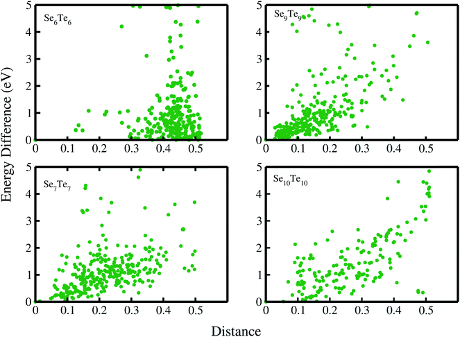 |
| | Fig. 3 DE plots for SenTen clusters. | |
The discretization of fingerprints, FAB(R), allows it to be represented as a vector. Each structure can thus be uniquely described by a fingerprint vector and the dissimilarity between structures can be calculated using the definition of distance,
| |  | (4) |
F
i,AB(k) represents the fingerprint of component i in the kth bin and
| |  | (5) |
is the weight factor of each fingerprint component. To characterize the molecular structures, configurational fingerprint vectors have been introduced.
53 They are the counterparts of the quantities used to identify the structures experimentally. The Euclidean distance between the configurational fingerprint vectors satisfies the properties of a metric and can therefore safely be used to measure dissimilarities between configurations in high dimensional configuration space. The normalized Euclidean distance
| |  | (6) |
measures the dissimilarly between structures
p and
q with no need to superimpose them.
F is a symmetric
N ×
N matrix whose elements depend only on the interatomic distances
rij = ‖
ri −
rj‖ of an n-atom configuration. Vectors
F containing eigenvalues of such a matrix form a configurational fingerprint, which allows the identification of a structure. In order to make Δ
D independent of the atomic indices, the elements of each
F are sorted in an ascending order. Computing the distance between two structures one quantifies the difference between them. Detailed discussion about fingerprint calculations is given in ref.
52 and
53. In DE plots,
Fig. 3, the obtained distance of isomers from the ground state is taken along the
x axis and the corresponding energy with respect to the global minima is taken along the
y axis. Such DE plots, in particular, have been used to infer
17 the glassy nature of clusters. In the present case, clusters are 1D ring-like structures and do reveal interesting features. Se
7Te
7 and Se
10Te
10 clusters show the presence of many low energy structures at small distances. It means that the structures are similar and very close to the ground state. In Se
6Te
6 and Se
9Te
9 however bunching of structures is seen. It implies that there are so many low energy structures, which are energetically close but structurally different than the ground state. From
Fig. 3, it is evident that enough configurations of a cluster exhibit local minima very close to the global minima, a distinct feature of glassy systems.
17 Thus, there exist enough geometries of similar energies separated by a barrier of different heights. Cooling through room temperature may leave any of these structures in the ground state. Any system having such metastable geometries are said to possess glassy nature. Such clusters may lead to the formation of amorphous solids
via rapid cooling
10 of these liquid clusters. The formation of such clusters in bulk alloys as well as on the surface of thin films
23 will make them to behave as amorphous materials. The amorphous nature of the Se–Te alloy has been well established in the experimental studies.
Shape analysis of these clusters has been done using the shape deformation parameter  , where Qx ≥ Qy ≥ Qz are the eigenvalues of the quadrupole tensor Qij = ∑IRIiRIj. Here RIi is the ith coordinate of ion I relative to the centre of mass.54,55 The eigenvalues of quadrupole tensors Qx, Qy, and Qz, as a function of cluster size are shown in Fig. 4. There is a significant change in the shape along the x direction compared to that in the y and z directions. It means that with an increase in the size of the cluster, it gets elongated (Qx > Qy). The variation in Qx, Qy and Qz shows a considerable change in the x and y directions, whereas along the z direction it is negligibly small. In the histogram, Fig. 4, for n = 5, 6 and 8, Qx ≃ Qy, which implies their circular shape, see Fig. 1.
 |
| | Fig. 4 Shape parameters Qx, Qy, and Qz as a function of sizes of clusters. | |
3.2 Raman and IR spectra
Vibrational spectroscopy is a commonly and widely used technique for the structure elucidation and identification of sustained impurities in a given material. The Raman spectra for the ground state geometries of SenTen clusters, n = 5–10, are shown in Fig. 5(a). The Raman intensities of phonon modes have been calculated from the derivative of a macroscopic dielectric tensor with respect to the normal mode coordinate.56 The observed Raman bands along with the assigned modes are presented in Table 3. The values given in the table are our results and superscripts a and b on values show that these values are consistent with the values reported in ref. 50 and 34. The occurrence of Se–Te bands is consistent with their structural arrangement, Fig. 1. The band at 214.7 cm−1 in the Se5Te5 geometry is ascribed to stretching vibration and the bands at 72.2 cm−1 and 59.3 cm−1 are assigned to the bending vibrations of Se–Te bonds. In the Se6Te6 cluster, Raman bands are observed at 211 cm−1 and 39 cm−1. The band at 211 cm−1 corresponds to stretching vibration in the Se–Te bond, whereas the band at 39 cm−1 shows the presence of a Te–Te bond not observed in the ring structure. The Raman spectra of Se7Te7, Se9Te9, and Se10Te10 clusters unveil the occurrence of Se–Se, Te–Te and Se–Te stretching and bending modes, Table 3. The Raman stretching modes observed in the spectral ranges 242–243, 197–233 and 173–194 cm−1 correspond to the stretching vibration of Se–Se, Se–Te and Te–Te bonds, respectively. The difference in the positions of the occurrence of Raman peaks may be ascribed to the difference in the structural parameters51 of these clusters. The emergence of Se–Se stretching and bending modes in Se9Te9 may be understood from its ring structure. Raman bands depicting the presence of homopolar bonds is a consequence of buckling in a ring structure that causes interaction between the nearest atoms. Bending Raman modes are noticed in the spectral ranges 100–108 and 60–75 cm−1 less than 50 cm−1 for Se–Se, Se–Te and Te–Te bonds, respectively. The noticed Raman bands are consistent with the Raman bands observed in a-Se, a-Te and Se–Te glass.34,50,57–62
 |
| | Fig. 5 (a) Raman and (b) infrared spectra of SenTen (n = 5–10) clusters. | |
Table 3 Raman and IR bands in SenTen clusters
| Clusters |
Raman ω (cm−1) |
Mode |
IR ω (cm−1) |
Mode |
|
Ref. 50.
Ref. 34.
|
| Se5Te5 |
214.7b |
Se–Te (stretching) |
213.9 |
Se–Te (stretching) |
|
|
72.2 |
Se–Te (bending) |
77.5a |
Se–Te (bending) |
|
|
59.3 |
Se–Te (bending) |
64.5 |
Se–Te (bending) |
| Se6Te6 |
211b |
Se–Te (stretching) |
216.5a |
Se–Te (stretching) |
|
|
39 |
Te–Te (bending) |
55.9 |
Se–Te (bending) |
| Se7Te7 |
222.9 |
Se–Te (stretching) |
222.9a |
Se–Te (stretching) |
|
|
221.5 |
Se–Te (stretching) |
221.5a |
Se–Te (stretching) |
|
|
207.7b |
Se–Te (stretching) |
221.4a |
Se–Te (stretching) |
|
|
182.1b |
Te–Te (stretching) |
182.5 |
Te–Te (stretching) |
|
|
173.4b |
Te–Te (stretching) |
182.1 |
Te–Te (stretching) |
|
|
106.3 |
Se–Se (bending) |
173.4a |
Te–Te (stretching) |
|
|
74.8 |
Se–Te (bending) |
98.4a |
Se–Se (bending) |
|
|
59.1 |
Se–Te (bending) |
72.2a |
Se–Te (bending) |
| Se8Te8 |
214.4a |
Se–Te (stretching) |
218.6a |
Se–Te (stretching) |
|
|
32.2 |
|
93.7a |
Se–Se (bending) |
| Se9Te9 |
242.9a,b |
Se–Se (stretching) |
242.9a |
Se–Se (stretching) |
|
|
242a,b |
Se–Se (stretching) |
242a |
Se–Se (stretching) |
|
|
232.9a |
Se–Se (stretching) |
215.4a |
Se–Te (stretching) |
|
|
224.3 |
Se–Te (stretching) |
214.3 |
Se–Te (stretching) |
|
|
217.6b |
Se–Te (stretching) |
210.9 |
Se–Te (stretching) |
|
|
210.9b |
Se–Te (stretching) |
202.6 |
Se–Te (stretching) |
|
|
200a |
Se–Te (stretching) |
197 |
Se–Te (stretching) |
|
|
197a |
Se–Te (stretching) |
196.6 |
Se–Te (stretching) |
|
|
108.4 |
Se–Se (bending) |
|
|
| Se10Te10 |
223.9 |
Se–Te (stretching) |
223.9a |
Se–Te (stretching) |
|
|
220.1 |
Se–Te (stretching) |
220.1a |
Se–Te (stretching) |
|
|
219.3 |
Se–Te (stretching) |
219.3 |
Se–Te (stretching) |
|
|
216.6b |
Se–Te (stretching) |
210.7 |
Se–Te (stretching) |
|
|
201.1a |
Se–Te (stretching) |
205.7 |
Se–Te (stretching) |
|
|
194.1a |
Se–Te (stretching) |
180.7 |
Te–Te (stretching) |
|
|
178.5b |
Te–Te (stretching) |
105.2a |
Se–Se (bending) |
|
|
99.7 |
Se–Se (bending) |
99.7a |
Se–Se (bending) |
|
|
36.7 |
|
91.5a |
Se–Se (bending) |
Stretching Se–Se, Se–Te and Te–Te bands in SexTe1−x glasses are observed34,57–62 at 250, 210 and 175 cm−1, respectively. Meanwhile in a DFT study34 of triatomic clusters, these bands were calculated to be in the spectral ranges 264–270, 218–230 and 180–183 cm−1, respectively. Our values for the Se–Se band are red shifted, whereas for Se–Te and Te–Te bands they are blue shifted in reference to experimental results. This difference may have been due to the absence of inter cluster interaction discussed in ref. 34. We have recorded the Raman spectra of individual clusters, whereas in glass they exist as a bunch of clusters. Our values are in good agreement with experimental values for Se–Te glasses, which shows that the Se–Te alloy, in the bulk form or in thin films, consists of ring structures.23,34,37
We have also examined the IR spectra of these clusters. IR intensities are computed from the eigenvectors and the Born effective-charge tensors. The Born effective charge tensor and the phonon eigenvectors are calculated from density functional perturbation theory (DFPT) implemented in the VASP code.56,63 Bands observed in IR spectra are also given in Table 3. Our results show the presence of Se–Se, Te–Te and Se–Te stretching and bending modes in the IR spectra in concurrence with Raman spectra. Se–Se, Te–Te and Se–Te IR stretching bands are ascertained in the spectral ranges 242.9–242, 173.4–182.5 and 196.6–222.9 cm−1, respectively. IR bands at lower frequencies, i.e., in the ranges 98.4–105.2, 45–49 and 55.7–99.7 cm−1, are assigned to the bending vibrations of Se–Se, Te–Te and Se–Te respectively. Our results are in agreement with the values reported for a− Se and SexTe1−x glasses or films.50,62
It is noticed that even the ground state structures of Se7Te7 and Se10Te10 clusters do not contain any homopolar bond, i.e., Se–Se or Te–Te bond, but Raman and IR spectra show the presence of Se–Se and Te–Te stretching and bending modes. The origin of these modes is the buckling in the ring structures. At the buckling point, a Se–Te–Se or Te–Se–Te trimer is formed. Depending upon the angle, the distance between two adjacent atoms may reduce and the Se/Te atom in one trimer starts to interact with the Se/Te atom of the second trimer. The occurrence of different bands at different wave numbers is ascribed to the difference in the bond length and bond angle.51 From Table 3, it is observed that IR active vibrational bands are also Raman active and surfaced more or less at the same wave number. Surfaced vibrational bands in the low frequency region, <100 cm−1, represent boson peaks. The appearance of boson peaks is a universal characteristic of glassy materials and they exist in all amorphous solids.60
Raman, IR and configurational studies reveal that the structural properties of SenTen clusters are consistent with Se–Te glass. It means that Se–Te glass is an ensemble of small clusters, each of which is in a configurationally disordered state. From the above discussion, we can say that SenTen clusters represent the microamorphous states of the bulk Se–Te system, because they can be realized experimentally. The structural parameters of SenTen clusters may differ from those of the Se–Te conventional system due to the fact that the experimentally acquired conventional amorphous system is not a true binary system.37
3.3 Energetics
The energy of the highest occupied molecular orbital (HOMO) and the lowest unoccupied molecular orbital (LUMO) for the least energy isomers (ground state) has been examined for each cluster. The difference in energy between the HOMO and LUMO refers to the chemical stability of clusters, Fig. 6(a). Clusters having a high value of the HOMO–LUMO gap (HLG) are considered more stable compared to other clusters.
 |
| | Fig. 6 (a) HOMO–LUMO gap and (b) BE per atom of SenTen clusters. | |
Binding energy per atom for ground state SenTen clusters as a function of cluster sizes is reported in Fig. 6(b). The maximum variation in B.E per atom is about 0.02 eV. In our previous work, we have studied pristine Sen and Ten clusters47 and observed that the values of the HL gap and BE per atom of SenTen clusters lie in between the values of pristine Sen and Ten clusters. This indicates that Se–Te clusters have intermediate behaviour between pure Se and Te clusters also observed in bulk Se–Te systems.27
The stability of SenTen clusters is also discussed in terms of ionization potential (IP) and electron affinity (EA). The ionization potential measures the energy difference between the ground state of the neutral and its cationic cluster, whereas the electron affinity is the energy difference between the ground state of the neutral and its anionic cluster. The IP and EA for the ground state structures are reported in Table 4. A high IP refer to more stability and less reactivity, whereas a high EA indicates high reactivity. The computed IP of these clusters lies between 4.89 and 5.61 eV, Table 4, which is lower than the IP of a-Se,64 9.75 eV, and a-Te,64 9 eV. Meanwhile the EA values are comparable to the values reported for Se,65 2.02 eV, and Te,66 1.97 eV. To investigate the effect of addition and removal of electrons on the charge distribution in a cluster, we have computed the charge density difference between the neutral and charged clusters. The charge density difference profile of the charged systems reveals that the electron and hole charge does not spill over to the vacuum region but is localized on the cluster (see Fig. S2, ESI†).
Table 4 Ionization potentials (IPs), electron affinities (EAs) and compositions of the HOMO and LUMO in SenTen clusters
|
|
IP (eV) |
EA (eV) |
HOMO |
LUMO |
| Se5Te5 |
5.61 |
2.69 |
0.20% s + 98.23% p |
8.95% s + 87.05% p |
| Se6Te6 |
5.42 |
2.49 |
98.82% p |
10.02% s + 85.77% p |
| Se7Te7 |
5.47 |
2.75 |
2.47% s + 95.82% p |
8.83% s + 87.14% p |
| Se8Te8 |
5.28 |
2.82 |
98.84% p |
9.72% s + 86.11% p |
| Se9Te9 |
4.89 |
2.59 |
0.38% s + 98.11% p |
10.02% s + 85.27% p |
| Se10Te10 |
5.01 |
2.77 |
98.26% p |
10.33% s + 85.19% p |
The nature of eigenvalues as a function of cluster size can be analysed from the energy eigenvalue spectrum. We have plotted the energy eigenvalue spectrum in Fig. 7. The black (blue) part of the spectrum is identified as occupied (unoccupied) orbitals. The reference energy for each cluster is with respect to the vacuum energy, which is zero. The occupied part of the spectrum consists of three well separated groups bunched together, similar to pristine Sen and Ten eigenvalue spectra.47 A splitting of energy levels in the lower group, except for n = 9, as well as in the upper group is observed. Band energy along with site projected s and p characters for n = 5 clusters is given in Table 5. Due to quasi-degeneracy, Table 5, the number of energy levels in a particular group is not clearly distinguishable. The nearly degenerate levels are reflected in the broadening of the line in the spectrum. The angular momentum character of the states can be analysed by examining the partial density of states (PDOS). The angular momentum projected density of states, a typical case for n = 5, is shown in ESI, Fig. S3.† The analysis of orbital electronic occupancies for different ground state structures discloses that the lowest group is mainly formed from atomic s orbitals and is well separated by an energy gap of ≥4.50 eV from the p group. The upper occupied group is formed mainly from pure p orbitals. All three px, py and pz orbitals are found to contribute to the formation of the upper group. It means that the lowest filled group is a result of pure s orbitals, whereas the upper group is a mixture of px, py and pz orbitals. The composition analysis of HOMO and LUMO levels, Table 4, shows that the contribution of the s component is about 0 to 3% in the HOMO orbital and 8 to 10% in the LUMO orbital. This indicates the least possibility of mixing of s and p orbitals, meaning no sp hybridization. The LUMO is separated at most by ∼2 eV from the HOMO, Fig. 7, consistent with our earlier results.47 The HOMO–LUMO gap determines the optical properties of a material. The HL gap of the investigated geometries concurs with the optical band gap of the amorphous Se(1−x)Tex system.26,67 Furthermore, our values of the HL gap, Table 1, are close to the reported energy gap of a-Se, 1.99 eV, and higher than that of a-Te, 0.5 eV.37
 |
| | Fig. 7 Eigenvalue spectrum for SenTen clusters. | |
Table 5 Band energy and s and p characters of molecular orbitals for n = 5
| Band |
Energy (eV) |
S (%) |
py (%) |
pz (%) |
px (%) |
Band |
Energy (eV) |
S (%) |
py (%) |
pz (%) |
px (%) |
| S1 |
−18.490 |
96.74 |
0.42 |
2.12 |
0.42 |
P1 |
−9.014 |
0 |
48.24 |
0 |
48.58 |
| S2 |
−18.211 |
96.07 |
0.84 |
1.83 |
0.84 |
P2 |
−8.973 |
4.13 |
54.04 |
22.44 |
17.59 |
| S3 |
−18.207 |
96.07 |
0.84 |
1.69 |
0.98 |
P3 |
−8.960 |
4.13 |
16.88 |
22.8 |
54.4 |
| S4 |
−17.530 |
94.54 |
1.91 |
0.82 |
2.05 |
P4 |
−8.383 |
8.79 |
22.71 |
44.51 |
23.26 |
| S5 |
−17.528 |
94.54 |
2.05 |
0.82 |
2.05 |
P5 |
−8.383 |
8.81 |
22.75 |
44.4 |
23.3 |
| S6 |
−15.304 |
91.05 |
3.92 |
0.42 |
3.92 |
P6 |
−7.747 |
3.18 |
44.16 |
8.28 |
43.52 |
| S7 |
−15.303 |
91.05 |
3.92 |
0.42 |
3.92 |
P7 |
−7.483 |
7.51 |
19.96 |
44.87 |
26.74 |
| S8 |
−14.122 |
93.42 |
3.49 |
0.81 |
1.88 |
P8 |
−7.481 |
7.82 |
21.64 |
47.64 |
22.18 |
| S9 |
−14.116 |
93.56 |
1.74 |
0.67 |
3.49 |
P9 |
−7.474 |
4.36 |
27.13 |
21.78 |
45.74 |
| S10 |
−13.479 |
96.83 |
0.13 |
2.64 |
0.13 |
P10 |
−7.469 |
3.99 |
51.9 |
19.16 |
23.95 |
|
|
|
|
|
|
|
P11 |
−6.326 |
5.45 |
10.48 |
68.76 |
11.32 |
|
|
|
|
|
|
|
P12 |
−6.079 |
0.79 |
45.04 |
10.71 |
42.06 |
|
|
|
|
|
|
|
P13 |
−6.077 |
0.79 |
44.05 |
10.71 |
43.06 |
|
|
|
|
|
|
|
P14 |
−5.947 |
3.13 |
29.1 |
64.64 |
1.29 |
|
|
|
|
|
|
|
P15 |
−5.933 |
3.13 |
0.92 |
65.19 |
28.91 |
|
|
|
|
|
|
|
P16 |
−5.450 |
1.96 |
1.96 |
90.96 |
3.14 |
|
|
|
|
|
|
|
P17 |
−5.220 |
3.55 |
5.72 |
39.25 |
48.52 |
|
|
|
|
|
|
|
P18 |
−5.213 |
3.54 |
48.62 |
38.98 |
5.91 |
|
|
|
|
|
|
|
P19 |
−5.026 |
0.2 |
47.15 |
4.72 |
46.56 |
|
|
|
|
|
|
|
P20 |
−5.024 |
0.2 |
47.15 |
4.72 |
46.37 |
|
|
|
|
|
|
|
P21 |
−3.220 |
8.95 |
36.19 |
24.95 |
25.9 |
|
|
|
|
|
|
|
P22 |
−3.208 |
8.94 |
26.81 |
24.33 |
35.93 |
|
|
|
|
|
|
|
P23 |
−3.078 |
6.76 |
36.87 |
17.18 |
36.68 |
|
|
|
|
|
|
|
P24 |
−2.420 |
9.49 |
22.08 |
41.61 |
22.08 |
|
|
|
|
|
|
|
P25 |
−2.310 |
8.46 |
18.27 |
35.38 |
32.31 |
|
|
|
|
|
|
|
P26 |
−1.995 |
3.86 |
47 |
11.59 |
28.33 |
3.4 Chemical bonding
Most of the properties of a material are determined by the nature of bonding in the material. The unusual stability of the clusters can be ascertained from the formation of different types of covalent bonds. We have examined the partial charge densities of individual MOs of ground state structures to understand the nature of bonding in SenTen clusters. The different ways in which orbitals overlap to form a covalent bond is the origin of the unusual stability of ring structures. Since s and p energy levels are far apart, there is no possibility of mixing of these energy levels. It shows that the bonds will have a dominant s or p character. The orientation of the Cartesian axis has been inserted in Fig. 8. The contributions of px, py and pz orbitals are provided in Table 5 for n = 5. It may be noted that the z-axis is perpendicular to the plane of the ring.
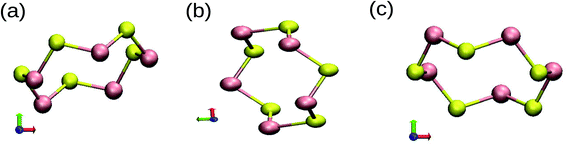 |
| | Fig. 8 Different geometries, (a)–(c), of SenTen cluster with the orientation of Cartesian axes. | |
We have examined the individual MOs of Se5Te5 clusters, Fig. 9, to understand the significant features of bonding. For analysis, we have considered 1/6th to 1/8th iso-surface values to the maximum value. The 1st molecular orbital of Se5Te5 is formed from pure s orbitals with the formation of delocalized sσ bonds, Fig. 9(a). The 11th MO is formed from purely p orbitals. Here, only the px and py components participate in the bonding, which forms a σ bond along the line joining the atoms, Fig. 9(f). The delocalization of charge is evident in the 1st and 11th MOs. As we go for higher MOs, the participation of py and pz components in the bond formation is realised. The 15th MO, Fig. 9(i), indicates the formation of three centred π orbitals, originating from buckling in the ring, along with an adjacent pσ bond.68 The formation of such three centred π orbitals facilitates distortion in the ring, necessary for the stability of one dimensional structures. Thus, bending or buckling is facilitated by the formation of pπ orbitals due to mixing of px, py and pz orbitals. In higher MOs, the delocalization nature of orbitals is not seen. The 30th and 31st MOs, i.e. HOMO and LUMO, consist of nonbonding and antibonding orbitals, Fig. 9(m) and (n). The HOMO along with the antibonding orbitals consists of nonbonding orbitals (lone pairs). The presence of lone pairs in a material facilitates the formation of amorphous structures. Furthermore, the 33rd MO consists of purely antibonding orbitals, Fig. 9(o). Since we have plotted the charge density of MOs, it is not possible to show the sign of the lobes, which makes the identification of bonding and anti-bonding MOs difficult. However, in some cases it is possible to identify the bonding and anti-bonding character of MOs from the nature of the iso-surface. The 1st, 2nd, and 3rd MOs in Fig. 9 reveal the bonding nature, whereas the 8th and 10th MOs show the anti-bonding nature of s MOs. The 11th, 12th, and 13th MOs represent pσ orbitals, the 15th, 16th, and 26th MOs represent pπ orbitals and the 29th, 30th, 31st and 33rd MOs reveal the presence of non-bonding and anti-bonding MOs.
 |
| | Fig. 9 Bonding, antibonding and non-bonding molecular orbitals of Se5Te5 clusters. | |
As noticed by Akola and Jones, the geometrical constraints imposed by closed ring structures may lead to an overlap of lone pairs with the nearest neighbour orbitals. So, it is instructive to show the manifestation of such an overlap by examining the charge density of some MOs, Fig. 9. We have shown the partial charge density iso-surface of a few MOs. The 15th MO, Fig. 9, reveals the occurrence of three and two centred bonds. The formation of two half rings one above and the other below the line joining the atoms can be clearly seen. It shows an interesting formation, X, of a bent pσ bond aided by the pz of Te and px and py orbitals of Se. Note that all three atoms, 2 atoms of Se and 1 atom of Te, participate in bonding. A similar formation, Y, is seen between the 2 atoms of Te and 1 atom of Se on the other side. The 16th MO shows the formation of an inner ring, displaying the presence of a multi-centred bond by the overlap of inner lobes of p orbitals, typically consisting of px and py orbitals. All the orbitals involved are perpendicular to the line joining the atoms. In other words, radially inward Te orbitals overlap and aid the formation of a bond between two nearest neighbour Se atoms. Since the orbitals are perpendicular to the bond axes, it is a π orbital formation.59 In the 26th MO, a peculiar orbital formation is observed. It shows a multi-centred π ring, in which alternate top and bottom lobes of pz orbitals of Se and Te overlap and give rise to a central ring. The nearest neighbour overlap comes from pz lobes on different sides (up and down). Although weak, the formation of yet another π orbital is revealed. The existence of such π orbitals has been noticed and discussed in the literature.59,69–75 The MO analysis of other clusters, n = 6–10, depicts the same features as observed in Se5Te5.
3.5 Optical properties
The real and imaginary parts of the dielectric function have been computed for most stable structures. The calculation of the dielectric function involves the electronic transitions between filled and empty states. The imaginary part of the dielectric function,  , is computed from the momentum matrix element between the filled and empty states using the relationship76–82
| |  | (7) |
where the indices α and β are the Cartesian components, êj is the unit vector along the direction of the electromagnetic field of energy ℏω, p is the momentum operator, e and m are the charge and mass of the bare electron, ψv and ψc are the filled and empty state eigenfunctions of the system and Ev and Ec are their corresponding energies. The momentum matrix is evaluated between filled and empty states using the corresponding eigenfunctions of each filled and empty state. Depending upon the size of the cluster, we have considered a minimum of 60 to 120 empty states to calculate  . We have varied the number of empty states to ascertain that the spectrum does not change appreciably with the number of empty states. We have plotted
  and
and  in Fig. S4 and S5† by varying the empty states for n = 5 and 10. It is observed that the increase or decrease in the number of empty states does not affect the spectra, remarkably. We found that the dielectric functions are converged with respect to the number of empty states for the entire energy window, Fig. S4 and S5.† Optical properties are reported to have functional dependence. To probe the functional dependence of optical properties, we have computed the dielectric functions using the B3LYP hybrid functional, Fig. 12 and 13. It is noted that the spectra obtained from the two functionals are consistent. The real part of the dielectric tensor ε′ can be obtained from the famous Kramers–Kronig transformation,
| |  | (8) |
where P denotes the principal value of the integral. Only interband transitions between valence and conduction states are taken into consideration.
The imaginary part of the dielectric function,  , for both in-plane polarization (E⊥C) and out-of-plane polarization (E∥C), is shown in Fig. 10.
  consists of sharp peaks for both in-plane and out-of-plane polarization. Peaks are characteristic features of discrete electronic states of clusters. The gap in the dielectric function (i.e. interval for which
  is zero) is about 1.6 eV in (E⊥C) and 2.71 eV in (E∥C) and matches the obtained HL gap of the clusters. It discloses the semiconducting behaviour of mixed clusters in analogy to pristine Sen and Ten clusters. Furthermore,
  reveals the pronounced absorption peaks between 2 and 8 eV. It is remarkable to point out that the optical response of the clusters along different orthogonal directions is not the same, and hence, clusters are no longer isotropic. The real part of the dielectric function
  is plotted in Fig. 11. It reveals the ability of a material to allow the passage of an electromagnetic field through it. The nature of bonding in a material has a significant impact on its electronic polarizability (optical dielectric constant, ε∞) and phonon polarizability (static dielectric constant, ε0). These quantities can be ascertained from the real dielectric function,
  . The bonding mechanism in amorphous materials83 can also be extracted from the static dielectric constant.
  , for clusters with n = 5, 8, and 10, has been obtained by extrapolating
  down to zero frequency. Its maximum values, 1.5, along E⊥C and 1.2, along E∥C, are in agreement with earlier reported values84 and indicate their feebly polar nature. The contribution of electronic polarizability (ε∞) is small compared to phonon polarizability.83,85 The dominance of
  divulges the presence of IR active phonons, corroborated by FTIR spectra. The small values of
  can be unequivocally attributed to the small difference (18%) in the electronegativity37 value of Se and Te. Thus, the dielectric study of SenTen clusters substantiates the covalent bonding, as discussed in the section Chemical bonding, and weak polarization in these clusters.47
 |
| | Fig. 10 Imaginary part of the dielectric function of clusters for polarization: (a) E⊥C and (b) E∥C. | |
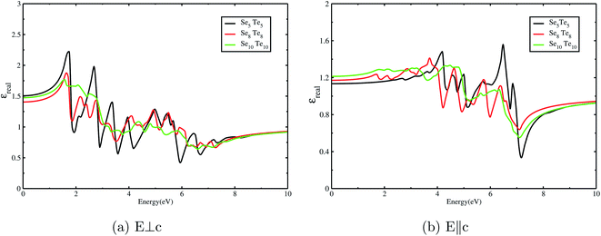 |
| | Fig. 11 Real part of the dielectric function of clusters for polarization: (a) E⊥C and (b) E∥C. | |
 |
| | Fig. 12 Dielectric function with PBE and B3LYP hybrid functionals for E⊥C. | |
 |
| | Fig. 13 Dielectric function with PBE and B3LYP hybrid functionals for E∥C. | |
The electron energy loss (EEL) function is computed from the real and imaginary parts of the dielectric function as
| |  | (9) |
The electron energy loss spectra (EELS) and absorption coefficient for the studied clusters are shown in Fig. 14. We have also ascertained that the variation in the number of empty states does not change the EELS substantially. In Fig. S6† we have plotted the EELS by varying the empty states for n = 5 and 10. An increase or decrease in the number of empty states does not affect the spectra, remarkably. We found that the EELS are converged with respect to the number of empty states for the entire energy window, Fig. S6.† Both spectra show prominent peaks in the range 2–8 eV. Resonant peaks in the EELS with fragmentation towards low as well as high energy represent the main plasma peaks.86 The fragmentation of peaks reveals87 the inhomogeneity in surface electron density. Peaks in the absorption coefficient reveal interband transitions between the HOMO and LUMO. The observed low energy excitations, below 8 eV, correspond to π band transitions. Because the electrons in the π orbital are loosely bound than the electrons in the σ orbital. The resonant peaks in the spectra E⊥C (E∥C) correspond to the π plasmon. Peak positions identify the plasmon frequency arising from the collective motion of π electrons. With an increase in the size of the cluster, a little shift and broadening in the resonant peaks is observed, also noticed in the EELS. It may be due to the fact that increase in size implies increase in polarizability and decrease in plasmon frequency.87 Also, the cluster size determines the surface plasmon energy,87 which decreases with increase in the size of the cluster. Furthermore, π plasmons are located in the ultraviolet (UV)-visible region. Strong absorption peaks in SenTen clusters, like Sin clusters,6 lie in the UV-visible region, whereas Se–Te alloys show high absorption in the visible reason.37 The intensity and position of absorption bands in UV-visible spectra are strongly influenced by the particle size, shape, concentration, composition and dielectric properties of clusters.88 Thus, the clusters with tunable optical properties can be designed simply by changing their size and composition. Absorption in the UV-visible region implies their use in the development of optoelectronic devices. Within the DFT framework, our results indicate that SenTen clusters may be potential candidates for the development of optoelectronic devices. The calculated value of the static refractive index for the studied clusters (n = 5–10) in E⊥C (E∥C) is 1.19(1.04), 1.15(1.07), 1.14(1.11), 1.16(1.06), 1.20(1.04), and 1.19(1.08). Our values of the static refractive index are close to the values reported for Se–Te glasses.89 The computed dielectric functions, EELS and absorption coefficient, using B3LYP and PBE functionals, are shown in Fig. 15 and 16. Their comparison shows some interesting features.  and
and  computed from the B3LYP functional do not show any change in the spectra except that the spectral peaks get shifted to higher energy with decrease in intensity. For the B3LYP functional, it is observed that peaks at lower energy occur with low intensity, whereas peaks at higher energy occur with high intensity in all spectra. B3LYP E⊥C EELS spectra for Se10Te10 reveal two more peaks of low intensity not observed in PBE spectra. The effect in E∥C is much pronounced; the first three peaks are suppressed and the main peak is enhanced by about 1.5. The B3LYP absorption coefficient for Se10Te10 is consistent with PBE spectra but the main peak is enhanced by about 1.5 times in both E⊥C and E∥C spectra. In all B3LYP spectra, the maximum shift in energy is about 1.35 eV. It is noteworthy that the B3LYP functional induces a blue shift in the optical properties of SenTen clusters. Experimental verification for the use of this functional is needed.
 |
| | Fig. 14 Electron energy loss spectra and absorption coefficient of SenTen clusters (E⊥C (black) and E∥C (red)). | |
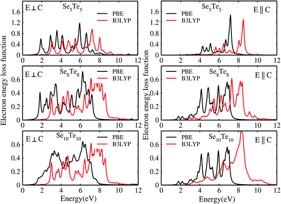 |
| | Fig. 15 Electron energy loss function with PBE and B3LYP hybrid functionals. | |
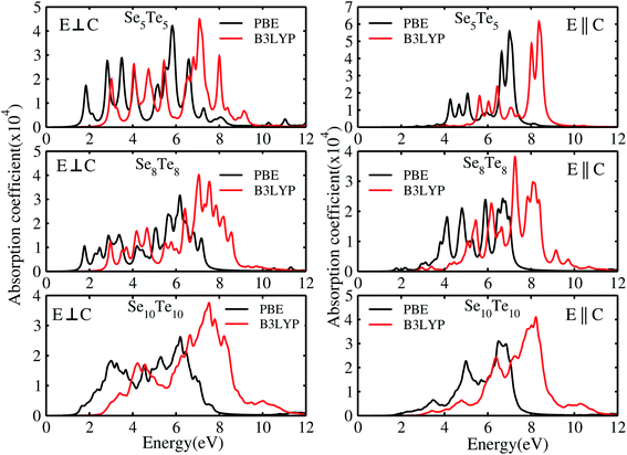 |
| | Fig. 16 Absorption coefficient with PBE and B3LYP hybrid functionals. | |
4 Summary and conclusion
We have presented the structural, electronic and optical properties of SenTen (n = 5–10) clusters. The initial geometries are obtained from a genetic algorithm based USPEX code. Structures were relaxed using the VASP code to their minima. About 50–60 structures of each cluster were examined to study their properties. The resulting structures are closed chain structures in concurrence with pristine Sen and Ten structures. The values of structural parameters, i.e., bond length and bond angle, correspond to the values reported for Se–Te glass. Ground state structures are purely formed from heteropolar Se–Te bonds, observed in previous simulations and experimental studies. The crystalfp code is employed to create distance energy plots. The DE plots reveal the presence of a large number of isomers having local minima close to their global minima. Raman and IR spectra describe the presence of Se–Te, Se–Se and Se–Te bonds in the ring structures, observed in Se–Te glass. Low frequency bands that surfaced in Raman and IR spectra are attributed to the presence of bosonic peaks, a universal feature of amorphous solids. The energy eigenvalue spectrum and nature of bonding in these clusters are consistent with Sen and Ten isolated clusters. The eigenvalue spectrum of ground state clusters shows a clear separation between the s and p orbitals. The nature of bonding has been analysed from the partial charge densities of individual molecular orbitals. The partial charge density of iso-surfaces reveals the presence of pσ and pπ orbitals. From the study of partial charge densities, it observed that the HOMO and LUMO of the investigated clusters consist of non-bonding and anti-bonding orbitals, respectively.
Optical properties are examined in terms of the dielectric constant, electron energy loss spectra (EELS) and absorption coefficient. A small value of the static dielectric constant establishes the covalent bonding and feebly polarizable nature of the clusters. The HL gap, originating from optical properties, matches well with the optical energy gap obtained from the imaginary part of the dielectric function. The energy loss spectra and absorption coefficient indicate the π-band transition that leads to the creation of π plasmons. Sharp peaks, between 2 and 8 eV, in  correspond to absorption peaks in the absorption coefficient. The plasmon frequency (ωp) decreases with increase in the size of the cluster, as observed in EEL spectra. The use of a hybrid functional (B3LYP) does not appreciably affect the form of the optical spectra. Absorption in the UV-visible region is unlike the absorption in Se–Te glasses. The present study shows that the properties of Se–Te glasses concur with the properties of SenTen clusters. Thus, SenTen clusters can be considered as a microamorphous state of the Se–Te alloy.
Author contributions
In the manuscript preparation all authors have contributed significantly. D. G. Kanhere was involved in supervision, conceptualization and acquiring resources. Raman Sharma has taken care of software, formal analysis and project administration. Tamanna Sharma has carried out the work. She contributed to data curation, formal analysis, validation and investigation.
Conflicts of interest
There is no conflict of interest to declare.
Acknowledgements
The authors acknowledge the HPC cluster facility created in the Department of Physics, Himachal Pradesh University, Summer Hill, Shimla, from the UGC FIST grant. Raman Sharma also acknowledges the help and discussion about distance energy plots with Balasaheb J. Nagare.
References
- F. Broghi, A. Podesta, C. Piazzoni and P. Milani, Growth mechanism of cluster assembled surfaces: from submonolayer to thin-film regime, Phys. Rev. Appl., 2018, 9(1–14), 044016 CrossRef.
- P. Mélinon, G. Fuchs, B. Cabaud, A. Hoareau, P. Jensen, V. Paillard and M. Treilleux, Low-energy cluster beam deposition: Do you need it?, J. Phys. IV, 1993, 3, 1585–1603 Search PubMed.
- A. N. Belov, S. V. Bulyarsky, D. G. Gromov, L. M. Pavlova and O. V. Pyatilova, Study of silver cluster formation from thin films on inert surface, CALPHAD: Comput. Coupling Phase Diagrams Thermochem., 2014, 44, 138–141 CrossRef CAS.
- S. N. Khanna and P. Jena, Atomic clusters: Building blocks for a class of solids, Phys. Rev., 1995, 51, 13705–13716 CAS.
- B. Chen, W. Sun, X. Kuang, G. L. Gutsev and C. Lu, Modification of Geometric and Electronic structure of Iron clusters by Nitrogen: Fe8−vs. Fe8N−, J. Phys. Chem. C, 2020, 124, 3867–3872 CrossRef CAS.
- A. Lehr, M. Jäger and R. Schäfer, Optical properties of Sin+ (n = 6–100) clusters: the approach to bulk behaviour, J. Phys. Chem. C, 2020, 124, 1070–1076 CrossRef CAS.
- J. Theerthagiri, K. Karuppasamy, G. Durai, A. U. H. S. Rana, P. Arunachalam, K. Sangeetha, P. Kappusami and H. S. Kim, Recent advances in metal chalcogenides (MX; X = S, Se) Nanostructures for electrochemical supercapacitors applications: a brief review, Nanomaterials, 2018, 8(1–28), 256 CrossRef PubMed.
- A. Jr Castleman and R. Keesee, Clusters: Properties and formation, Annu. Rev. Phys. Chem., 1986, 37, 525–550 CrossRef.
- D. Y. Sun and X. G. Gong, Structural properties and glass transition in Aln clusters, Phys. Rev. B: Condens. Matter Mater. Phys., 1998, 57, 4730–4735 CrossRef CAS.
- J. P. Rose and R. S. Berry, (KCl)32 and the possibilities for glassy clusters, J. Chem. Phys., 1993, 98, 3262–3274 CrossRef CAS.
- D. Vollath, D. Holec and F. D. Fischer, Au55, a stable glassy cluster: results of ab initio calculations, J. Nanotechnol., 2017, 8, 2221–2229 CAS.
- J. Y. Yi, D. J. Oh and J. Bernholc, Structural Distortions in Metal Clusters, Phys. Rev. Lett., 1991, 67, 1594–1597 CrossRef CAS PubMed.
- A. Sachdev, R. I. Masel and J. B. Adams, An Embedded Atom Method study of the equilibrium shapes of small platinum and palladium clusters, Z. Phys. D, 1993, 26, 310–312 CrossRef CAS.
- U. Rothlisberger, W. Andreoni and P. Glannozzi, Thirteen-atom clusters: Equilibrium geometries, structural transformations, and trends in Na, Mg, AI, and Si, J. Chem. Phys., 1992, 96, 1248–1256 CrossRef.
- S. Debiaggi and A. Caro, Structural study of Al147, Phys. Rev. B: Condens. Matter Mater. Phys., 1992, 46, 7322–7325 CrossRef CAS PubMed.
- A. Bulgac and D. Kusnezov, Thermal Properties of Na8 Microclusters, Phys. Rev. Lett., 1992, 68, 1335–1338 CrossRef CAS PubMed.
- S. De, B. Schaefer, A. Sadeghi, M. Sicher, D. G. Kanhere and S. Goedecker, Relation between the Dynamics of Glassy Clusters and Characteristic Features of their Energy Landscape, Phys. Rev. Lett., 2014, 112(1–5), 083401 CrossRef.
-
Z. H. Ebrahiminejad, S. F. Masoudi, R. S. Dariani and S. Jahromi, Thin Film Growth by Using Random Shape Cluster Deposition, arXiv:1205.3956v2[Cond-Mat.mes-hall], 08 Nov. 2012 Search PubMed.
- Z. H. Khan, S. A. Khan, S. Habib, A. A. Al-Ghamdi and N. Salah, Morphology and optical properties of thin films of GaxSe100−x nanoparticles, Nanosci. Nanotechnol. Lett., 2011, 3, 319–323 CrossRef CAS.
- Z. H. Khan, S. A. Khan, N. Salah, S. S. Habib and A. A. Al-Ghamdi, Electrical transport properties of thin film of a-Se87Te13 nanorods, J. Exp. Nanosci., 2011, 6, 337–348 CrossRef CAS.
- Z. H. Khan, S. A. Khan, N. Salah, A. A. Al-Ghamdi and S. Habib, Electrical properties of thin films of a-GaxTe100−x composed of nanoparticles, Philos. Mag. Lett., 2011, 91, 207–213 CrossRef CAS.
- N. Salah, S. S. Habib, Z. H. Khan, E. Alarfaj and S. A. Khan, Synthesis and Characterization of Se35Te65−xGex Nanoparticle Films and Their Optical Properties, J. Nanomater., 2012,(1–9), 393084 Search PubMed.
- Z. H. Khan, N. Salah, S. Habib, A. A. Al-Ghamdi and S. A. Khan, Electrical and optical properties of a-SexTe100−x thin films, Opt. Laser Technol., 2012, 44(1), 6–11 CrossRef CAS.
- E. H. Sondheimer, The mean free path of electrons in metals, Adv. Phys., 1952, 1(1), 1–42 CrossRef.
- A. F. Mayadas and M. Shatzkes, Electrical-resistivity model for polycrystalline films: The case of arbitrary reflection at external surfaces, Phys. Rev. B: Condens. Matter Mater. Phys., 1970, 1, 1382–1389 CrossRef.
- F. A. Al-Agel, Optical and structural properties of amorphous SexTe100−x aligned nanorods, Nanoscale Res. Lett., 2013, 8(1–9), 520 CrossRef PubMed.
- Z. H. Khan, A. A. Al-Ghamdib and F. A. Al-Agelb, Crystallization kinetics in as-synthesis high yield of a-Se100−xTex nanorods, Mater. Chem. Phys., 2012, 134, 260–265 CrossRef CAS.
- N. Salah, A. S. S. Habib, A. Memic, N. D. Alharbi, S. S. Babkair and Z. H. Khan, Syntheses and characterization of thin films of Te94Se6 nanoparticles for semiconducting and optical devices, Thin Solid Films, 2013, 531, 70–75 CrossRef CAS.
- N. Salah, S. S. Habib and Z. H. Khan, Direct bandgap materials based on the thin films of SexTe100−x nanoparticles, Nanoscale Res. Lett., 2012, 7(1–8), 509 CrossRef PubMed.
- K. Tripathi, A. A. Bahishti, M. A. Majeed Khan, M. Husain and M. Zulfequar, Optical properties of selenium-tellurium nanostructured thin film grown by thermal evaporation, Phys. B, 2009, 404, 2134–2137 CrossRef CAS.
- Z. H. Khan, M. M. Malik, M. Zulfequar and M. Husain, Electrical conduction mechanism in a-Se80−xTexGa20 films (x < or = x < or = 20), J. Condens. Matter Phys., 1995, 7, 8979–8991 CrossRef CAS.
- Z. H. Khan, M. Zulfequar, M. M. Malik and M. Husain, Electrical transport properties of thin films of a-Se80−xGa20Bix, Mater. Sci. Technol., 1997, 13, 484–489 CrossRef CAS.
- Z. H. Khan, M. Zilfequar, M. Ilyas and M. Husain, Electrical Conductivity and Thermoelectric Power of a-Se80−xGa20Tex (x = 0, 5, 10, 15 and 20) Thin Films, Acta Phys. Pol., A, 2000, 98, 93–98 CrossRef CAS.
- A. Tverjanovich, A. Cuisset, D. Fontanari and E. Bychkov, Structure of Se-Te glasses by Raman spectroscopy and DFT modeling, J. Am. Ceram. Soc., 2018, 1–10, 5188–5197 CrossRef.
- K. Itoh, Structure of Se-Te glasses studied using neutron, X-ray diffraction and reverse Monte Carlo modeling, J. Solid State Chem., 2017, 246, 372–378 CrossRef CAS.
- B. Bureau, C. Boussard-Plédel, M. LeFloch, J. Troles, F. Smektala and J. Lucas, Selenium-tellurium sequences in binary glasses as depicted by 77Se and 125Te NMR, J. Phys. Chem. B, 2005, 109, 6130–6135 CrossRef CAS PubMed.
- K. V. Reddy and A. K. Bhatnagart, Electrical and optical studies on amorphous Se-Te alloys, J. Phys. D: Appl. Phys., 1992, 25, 1810–1816 CrossRef CAS.
- C. W. Glass, A. R. Oganov and N. Hansen, USPEX - Evolutionary crystal structure prediction, Comput. Phys. Commun., 2006, 175, 713–720 CrossRef CAS.
- A. R. Oganov, A. O. Lyakhov and M. Valle, How Evolutionary Crystal Structure Prediction Works and Why, Acc. Chem. Res., 2011, 44, 227–237 CrossRef CAS PubMed.
- G. Kresse and J. Hafner, Ab initio Molecular Dynamics for Liquid Metal, Phys. Rev. B: Condens. Matter Mater. Phys., 1993, 47, 558–561 CrossRef CAS PubMed.
- G. Kresse and J. Furthmuller, Efficient iterative schemes for ab initio total-energy calculations using a plane-wave basis set, Phys. Rev. B: Condens. Matter Mater. Phys., 1996, 54, 11169–11186 CrossRef CAS PubMed.
-
G. Kresse and J. Furthmuller, VASP the GUIDE, 2005 Search PubMed.
- J. P. Perdew, K. Burke and M. Ernzerhof, Generalized Gradient Approximation Made Simple, Phys. Rev. Lett., 1996, 77, 3865–3868 CrossRef CAS PubMed.
- J. P. Perdew, K. Burke and M. Ernzerhof, Generalized Gradient Approximation Made Simple, Phys. Rev. Lett., 1997, 78, 1396 CrossRef CAS.
- M. Valle and A. R. Oganov, Crystal fingerprint space - a novel paradigm for studying crystal-structure sets, Acta Crystallogr., Sect. A: Found. Crystallogr., 2010, 66, 507–517 CrossRef CAS PubMed.
- M. Majid, S. Bénazeth, C. Souleau and J. Purans, XAFS study of interchain and intrachain order in Se1−xTex glasses: Nearest neighbors, Phys. Rev. B: Condens. Matter Mater. Phys., 1998, 58, 6104–6114 CrossRef CAS.
- T. Sharma, R. Sharma, R. A. Tamboli and D. J. Kanhere, Ab initio investigation of structural and electronic properties of selenium and tellurium clusters, Eur. Phys. J. B, 2019, 92(1–14), 51 CrossRef.
- L. A. Silva and M. Cutler, Optical properties of liquid Se-Te alloys, Phys. Rev. B: Condens. Matter Mater. Phys., 1990, 42, 7103–7113 CrossRef CAS PubMed.
- S. Datta, A. K. Raychaudhuri and T. Saha-Dasgupta, First principles study of bimetallic N13−nAgn nano-clusters (n = 0–13): structural, mixing, electronic and magnetic properties, J. Chem. Phys., 2017, 146, 164301 CrossRef PubMed.
- P. Heera and R. Sharma, Spectroscopic analysis of Sn doped Se-Te glassy alloy, J. Non-Cryst. Solids, 2016, 437, 87–92 CrossRef CAS.
- A. Rana, B. P. Singh and R. Sharma, Structural and chemical changes in Ga doped Ge-S glassy alloy, J. Non-Cryst. Solids, 2019, 523(1–8), 119597 CrossRef CAS.
- A. R. Oganov and M. Valle, How to quantify energy landscapes of solids, J. Chem. Phys., 2009, 130(1–9), 104504 CrossRef PubMed.
- A. Sadeghi, S. A. Ghasemi, B. Schaefer, S. Mohr, M. A. Lill and S. Goedecker, Metrics for measuring distances in configuration spaces, J. Chem. Phys., 2013, 139, 184118 CrossRef PubMed.
- I. Heidari, S. De, S. M. Ghazi, S. Goedecker and D. G. Kanhere, Growth and Structural Properties of MgN (N = 10–56) Clusters: Density Functional Theory Study, J. Phys. Chem. A, 2011, 115, 12307–12314 CrossRef CAS PubMed.
- S. M. Ghazi and D. G. Kanhere, Thermodynamic Properties of Ga27Si3 Cluster Using Density Functional Molecular Dynamics, J. Phys. Chem. A, 2012, 116, 11–17 CrossRef CAS PubMed.
- D. Yao, Y. D. Xu, C. Wang, Y. Y. Lv, Y. B. Chen, S. H. Yaoacd and H. Zhou, Infrared and Raman spectra of Bi2O2X and Bi2OX2 (X = S, Se, and Te) studied from first principles calculations, RSC Adv., 2019, 9, 18042 RSC.
- A. T. Ward, Investigation of Amorphous Chalcogenide Alloys Using Laser Raman Spectroscopy, Adv. Chem., 1972, 110, 163–178 CrossRef CAS.
- M. H. Brodsky, R. J. S. Gambino, J. E. Smith and Y. Yacoby, The Raman spectrum of amorphous Tellurium, Phys. Status Solidi, 1972, 52, 609–614 CrossRef CAS.
- J. Akola and R. O. Jones, Structure and dynamics in amorphous tellurium and Ten clusters: a density functional study, Phys. Rev. B: Condens. Matter Mater. Phys., 2012, 85(1–12), 134103 CrossRef.
- A. A. Baganich, V. I. Mikla, D. G. Semak, A. P. Sokolov and A. P. Shebanin, Raman scattering in amorphous Selenium, Phys. Status Solidi, 1991, 166, 297–302 CrossRef CAS.
- A. H. Goldan, C. Li, S. J. Pennycook, J. Schneider, A. Blom and W. Zhao, Molecular Structure of vapour-deposited amorphous selenium, J. Appl. Phys., 2016, 120(1–9), 135101 CrossRef.
- K. Nagata, k. Ishibashi and y. Miyamoto, Raman and Infrared spectra of rhombohedral selenium, Jpn. J. Appl. Phys., 1981, 20, 463–469 CrossRef CAS.
- A. Roy, S. Mukherjee, R. Gupta, S. Auluck, R. Prasad and A. Garg, Electronic structure, Born effective charges and spontaneous polarization in magnetoelectric gallium ferrite, J. Phys.: Condens. Matter, 2011, 23(1–9), 325902 CrossRef PubMed.
-
Ionization potentials of atoms and atomic ions in Handbook of Chem. and Phys., D. R. Lide, 1992, pp. 10–211 Search PubMed.
- M. Vandevraye, C. Drag and C. Blondel, Electron affinity of selenium measured by photodetachment microscopy, Phys. Rev. A, 2012, 85(1), 015401 CrossRef.
- G. Haeffler, A. E. Klinkmüller, J. Rangell, U. Berzinsh and D. Hanstorp, The Electron Affinity of Tellurium, Z. Phys. D, 1996, 38(3), 211 CrossRef CAS.
- H. El-Zahed, M. A. Khaled, A. El-Korashy, S. M. Youssef and M. El. Ocker, Dependence of optical band gap on the compositions of Se(1−x)Tex thin films, Solid State Commun., 1994, 89, 1013–1016 CrossRef CAS.
- P. Ghosh, J. Bhattacharjee and U. V. Waghmare, The Origin of Stability of Helical Structure of Tellurium, J. Phys. Chem. C, 2008, 112, 983–989 CrossRef CAS.
- G. Orlova and J. D. Goddard, Density Functional Study of Tetra-Atomic Clusters and Complexes of the Group 16 Elements: Trends in Structure and Bonding, J. Phys. Chem. A, 1999, 103(34), 6825–6834 CrossRef CAS.
- K. Tanaka, Excitation-induced effects in selenium clusters: molecular-orbital analyses, J. Optoelectron. Adv. Mater., 2017, 19, 586–594 CAS.
- Z. O. Li, J. Z. Yu and K. Ohno, Electronic states and stability of selenium clusters, Phys. Rev. B: Condens. Matter Mater. Phys., 1995, 52, 1524–1527 CrossRef CAS PubMed.
- H. J. Choi, Tellurium Clusters (125Tem) and Their Electronic Structures with Mossbauer Couplings, J. Korean Phys. Soc., 1998, 30, 562–570 Search PubMed.
- T. H. Lee and S. R. Elliott, Chemical Bonding in Chalcogenides: The Concept of Multicenter Hyperbonding, Adv. Mater., 2020, 32, 200340 Search PubMed.
- T. Chivers and R. S. Laitinen, Tellurium: a maverick among the chalcogens, Chem. Soc. Rev., 2015, 44, 1725–1739 RSC.
- V. S. Ghemud, H. A. Shafiei Gol and A. Kshirrsagar, How different are Te clusters- a first principles study, J. Nanopart. Res., 2018, 20, 177 CrossRef.
- X. D. Zhang, M. L. Guo, D. Wu, P. X. Liu, Y. M. Sun, L. Zhang, Y. She, Q. F. Liu and F. Y. Fan, First-Principles Investigation of Ag-Doped Gold Nanoclusters, Int. J. Mol. Sci., 2011, 12, 2972–2981 CrossRef CAS PubMed.
- C. Noguez and S. E. Ulloa, First-principles calculations of optical properties: Application to silicon clusters, Phys. Rev. B: Condens. Matter Mater. Phys., 1997, 56, 9719–9725 CrossRef CAS.
- D. Singh, S. K. Gupta, Y. Sonvanea and I. Lukacevic, Antimonene: a monolayer material for ultraviolet optical nanodevices, J. Mater. Chem. C, 2016, 4, 6386–6390 RSC.
- P. Rani, G. S. Dubey and V. K. Jindal, study of optical properties of pure and doped graphene, Phys. E, 2014, 62, 28–35 CrossRef CAS.
- X. D. Zhang, M. L. Guo, W. X. Li and C. L. Liu, First-principles study of electronic and optical properties in wurtzite Zn1−xCdxO, J. Appl. Phys., 2008, 103(1–6), 06372 Search PubMed.
- X. D. Zhang, M. L. Guo, C. L. Liu, W. X. Li and X. F. Hong, Electronic and optical properties of Ti1−xCdxO2: a first principles prediction, Appl. Phys. Lett., 2008, 93(1–3), 012103 CrossRef.
- M. Gajdoš, K. Hummer and G. Kresse, Linear optical properties in the projector-augmented wave methodology, Phys. Rev. B: Condens. Matter Mater. Phys., 2006, 73(1–9), 045112 CrossRef.
- C. Chen, P. Jost, H. Volker, M. Kaminski, M. Wirtssohn, U. Engelmann, K. Krüger, F. Schlich, C. Schlockermann, R. P. S. M. Lobo and M. Wuttig, Dielectric properties of amorphous phase-change materials, Phys. Rev. B: Condens. Matter Mater. Phys., 2017, 95(1–9), 094111 CrossRef.
- H. P. D. Lanyon, Optical and Electrical properties of Selenium-Tellurium Alloys, J. Appl. Phys., 1964, 35, 1516–1523 CrossRef CAS.
- D. Lencer, M. Salinga and M. Wuttig, Design Rules for Phase-Change Materials in Data Storage Applications, Adv. Mater., 2011, 23(18), 2030–2058 CrossRef CAS PubMed.
- R. Moradian, M. Shahrokhi, S. S. Charganeh and S. Moradian, Structural, magnetic, electronic and optical properties of iron cluster (Fe6) decorated boron nitride sheet, Phys. E, 2012, 46, 182–188 CrossRef CAS.
- A. Rubio, J. A. Alonso and J. M. López, Surface plasmon excitations in C60, C60K and C60H clusters, Phys. B, 1993, 183, 247–263 CrossRef CAS.
- C. Sönnichsen, T. Franzl, T. Wilk, G. v. Plessen and J. Feldmann, Plasmon resonances in large noble-metal clusters, New J. Phys., 2002, 4, 93.1–93.8 CrossRef.
- M. Mishra, R. Chauhan, A. Katiyar and K. K. Srivastava, Optical properties of amorphous thin film of Se-Te-Ag system prepared by using thermal evaporation technique, Prog. Nat. Sci.: Mater. Int., 2011, 21, 36–39 CrossRef.
Footnote |
| † Electronic supplementary information (ESI) available. See DOI: 10.1039/d1na00321f |
|
| This journal is © The Royal Society of Chemistry 2022 |
Click here to see how this site uses Cookies. View our privacy policy here. 
 Open Access Article
 This Open Access Article is licensed under a Creative Commons Attribution-Non Commercial 3.0 Unported Licence
 *a and
D. G.
Kanhere
b
*a and
D. G.
Kanhere
b


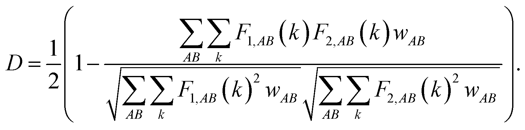


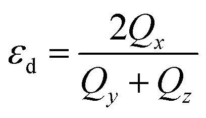 , where Qx ≥ Qy ≥ Qz are the eigenvalues of the quadrupole tensor Qij = ∑IRIiRIj. Here RIi is the ith coordinate of ion I relative to the centre of mass.54,55 The eigenvalues of quadrupole tensors Qx, Qy, and Qz, as a function of cluster size are shown in Fig. 4. There is a significant change in the shape along the x direction compared to that in the y and z directions. It means that with an increase in the size of the cluster, it gets elongated (Qx > Qy). The variation in Qx, Qy and Qz shows a considerable change in the x and y directions, whereas along the z direction it is negligibly small. In the histogram, Fig. 4, for n = 5, 6 and 8, Qx ≃ Qy, which implies their circular shape, see Fig. 1.

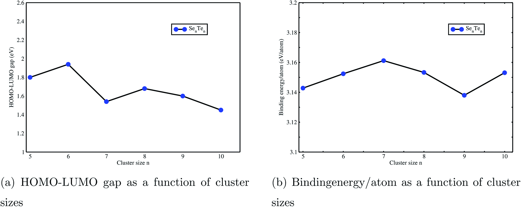


 , is computed from the momentum matrix element between the filled and empty states using the relationship76–82
 . We have varied the number of empty states to ascertain that the spectrum does not change appreciably with the number of empty states. We have plotted
  and
and  in Fig. S4 and S5† by varying the empty states for n = 5 and 10. It is observed that the increase or decrease in the number of empty states does not affect the spectra, remarkably. We found that the dielectric functions are converged with respect to the number of empty states for the entire energy window, Fig. S4 and S5.† Optical properties are reported to have functional dependence. To probe the functional dependence of optical properties, we have computed the dielectric functions using the B3LYP hybrid functional, Fig. 12 and 13. It is noted that the spectra obtained from the two functionals are consistent. The real part of the dielectric tensor ε′ can be obtained from the famous Kramers–Kronig transformation,
 , for both in-plane polarization (E⊥C) and out-of-plane polarization (E∥C), is shown in Fig. 10.
  consists of sharp peaks for both in-plane and out-of-plane polarization. Peaks are characteristic features of discrete electronic states of clusters. The gap in the dielectric function (i.e. interval for which
  is zero) is about 1.6 eV in (E⊥C) and 2.71 eV in (E∥C) and matches the obtained HL gap of the clusters. It discloses the semiconducting behaviour of mixed clusters in analogy to pristine Sen and Ten clusters. Furthermore,
  reveals the pronounced absorption peaks between 2 and 8 eV. It is remarkable to point out that the optical response of the clusters along different orthogonal directions is not the same, and hence, clusters are no longer isotropic. The real part of the dielectric function
  is plotted in Fig. 11. It reveals the ability of a material to allow the passage of an electromagnetic field through it. The nature of bonding in a material has a significant impact on its electronic polarizability (optical dielectric constant, ε∞) and phonon polarizability (static dielectric constant, ε0). These quantities can be ascertained from the real dielectric function,
  . The bonding mechanism in amorphous materials83 can also be extracted from the static dielectric constant.
  , for clusters with n = 5, 8, and 10, has been obtained by extrapolating
  down to zero frequency. Its maximum values, 1.5, along E⊥C and 1.2, along E∥C, are in agreement with earlier reported values84 and indicate their feebly polar nature. The contribution of electronic polarizability (ε∞) is small compared to phonon polarizability.83,85 The dominance of
  divulges the presence of IR active phonons, corroborated by FTIR spectra. The small values of
  can be unequivocally attributed to the small difference (18%) in the electronegativity37 value of Se and Te. Thus, the dielectric study of SenTen clusters substantiates the covalent bonding, as discussed in the section Chemical bonding, and weak polarization in these clusters.47


 and
and  computed from the B3LYP functional do not show any change in the spectra except that the spectral peaks get shifted to higher energy with decrease in intensity. For the B3LYP functional, it is observed that peaks at lower energy occur with low intensity, whereas peaks at higher energy occur with high intensity in all spectra. B3LYP E⊥C EELS spectra for Se10Te10 reveal two more peaks of low intensity not observed in PBE spectra. The effect in E∥C is much pronounced; the first three peaks are suppressed and the main peak is enhanced by about 1.5. The B3LYP absorption coefficient for Se10Te10 is consistent with PBE spectra but the main peak is enhanced by about 1.5 times in both E⊥C and E∥C spectra. In all B3LYP spectra, the maximum shift in energy is about 1.35 eV. It is noteworthy that the B3LYP functional induces a blue shift in the optical properties of SenTen clusters. Experimental verification for the use of this functional is needed.
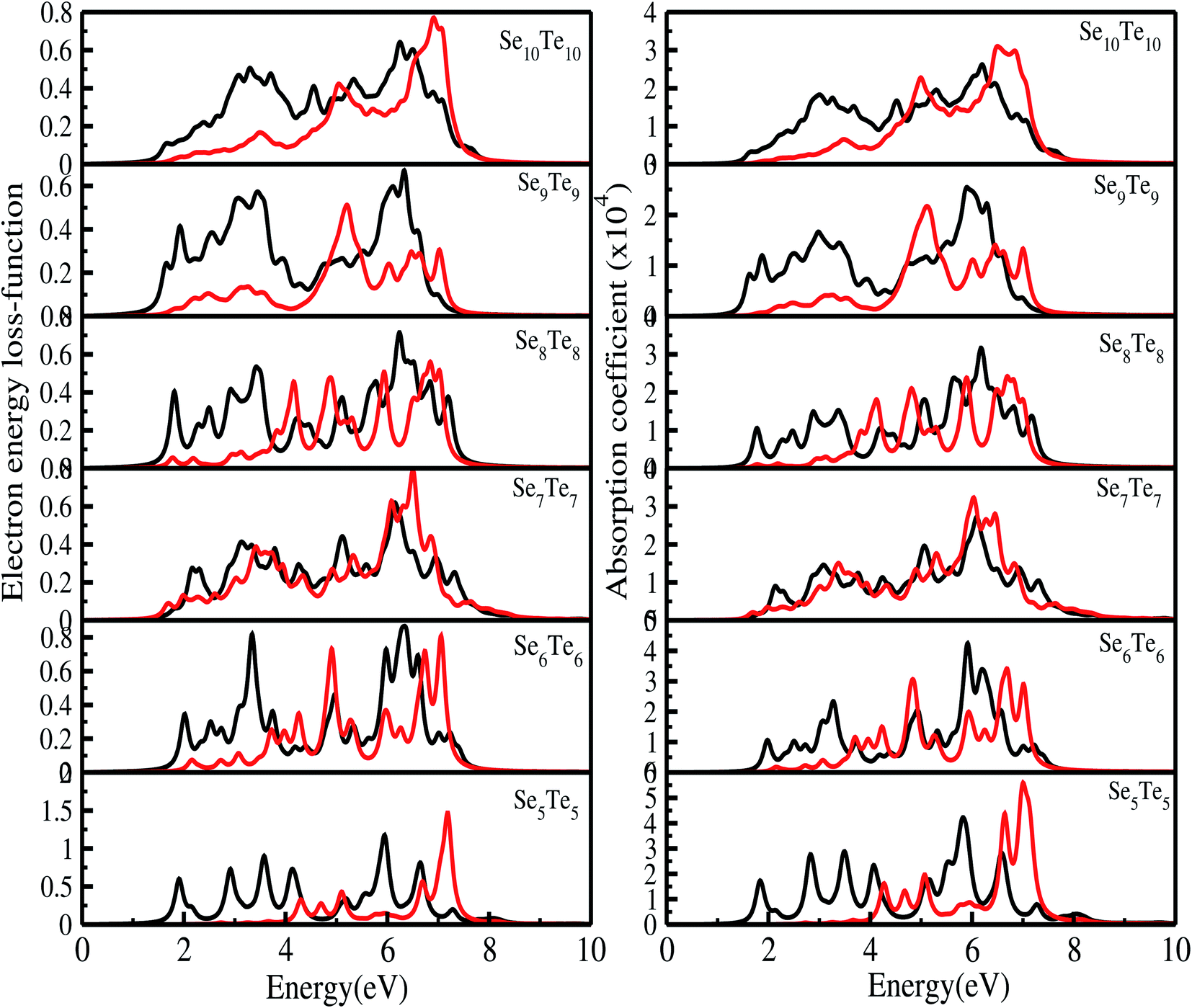


 correspond to absorption peaks in the absorption coefficient. The plasmon frequency (ωp) decreases with increase in the size of the cluster, as observed in EEL spectra. The use of a hybrid functional (B3LYP) does not appreciably affect the form of the optical spectra. Absorption in the UV-visible region is unlike the absorption in Se–Te glasses. The present study shows that the properties of Se–Te glasses concur with the properties of SenTen clusters. Thus, SenTen clusters can be considered as a microamorphous state of the Se–Te alloy.