
 Open Access Article
 This Open Access Article is licensed under a Creative Commons Attribution-Non Commercial 3.0 Unported Licence
Identification of multi-color emission from coaxial GaInN/GaN multiple-quantum-shell nanowire LEDs
Kazuma
Ito†
a,
Weifang
Lu†
 *a,
Sae
Katsuro
a,
Renji
Okuda
a,
Nanami
Nakayama
a,
Naoki
Sone
ac,
Koichi
Mizutani
d,
Motoaki
Iwaya
a,
Tetsuya
Takeuchi
a,
Satoshi
Kamiyama
a and
Isamu
Akasaki
ab
*a,
Sae
Katsuro
a,
Renji
Okuda
a,
Nanami
Nakayama
a,
Naoki
Sone
ac,
Koichi
Mizutani
d,
Motoaki
Iwaya
a,
Tetsuya
Takeuchi
a,
Satoshi
Kamiyama
a and
Isamu
Akasaki
ab
aDepartment of Materials Science and Engineering, Meijo University, 1-501 Shiogamaguchi, Tenpaku-ku, Nagoya, 468-8502, Japan. E-mail: weif@meijo-u.ac.jp; nianyulu@outlook.com
bAkasaki Research Center, Nagoya University, Furo-cho, Chikusa-ku, Nagoya 460-8601, Japan
cKoito Manufacturing Co., LTD., Tokyo 108-8711, Japan
dTOYODA GOSEI Co., Ltd., Aichi 492-8542, Japan
First published on 13th October 2021
Abstract
Multi-color emission from coaxial GaInN/GaN multiple-quantum-shell (MQS) nanowire-based light-emitting diodes (LEDs) was identified. In this study, MQS nanowire samples for LED processes were selectively grown on patterned commercial GaN/sapphire substrates using metal–organic chemical vapor deposition. Three electroluminescence (EL) emission peaks (440, 540, and 630 nm) were observed, which were primarily attributed to the nonpolar m-planes, semipolar r-planes, and the polar c-plane tips of nanowire arrays. A modified epitaxial growth sequence with improved crystalline quality for MQSs was used to effectively narrow the EL emission peaks. Specifically, nanowire-based LEDs manifested a clear redshift from 430 nm to 520 nm upon insertion of AlGaN spacers after the growth of each GaInN quantum well. This demonstrates the feasibility of lengthening the EL emission wavelength since an AlGaN spacer can suppress In decomposition of the GaInN quantum wells during ramping up the growth temperature for GaN barriers. EL spectra showed stable emission peaks as a function of the injection current, verifying the critical feature of the non-polarization of GaN/GaInN MQSs on nanowires. In addition, by comparing EL and photoluminescence spectra, the yellow-red emission linked to the In-fluctuation and point defects in the c-plane MQS was verified by varying the activation annealing time and lowering the growth temperature of the GaInN quantum wells. Therefore, optimization of MQS nanowire growth with a high quality of c-planes is considered critical for improving the luminous efficiency of nanowire-based micro-LEDs/white LEDs.
1. Introduction
With the recent proliferation of 5G technology and the increasing demand for more immersive environments for augmented reality (AR) and virtual reality (VR), more high-performance electronic technologies are expected. Among these technologies, micro-light-emitting diodes (LEDs) are gaining popularity because they can offer higher light brightness, faster response time, higher resolution, and lower power consumption than do current liquid crystal displays (LCD) and organic LED (OLED) displays.1–7 In particular, group III nitride semiconductors, which can cover the entire wavelength range of visible light, are promising for the realization of high-performance white LEDs/micro-LEDs.8,9 Although there have been marvelous advancements in nitride LEDs using the polar plane (c-plane) as the light-emitting region, the progress has reached a ceiling for the dramatically increasing requirement in AR, VR, and other modern display systems in the future. In addition, the quantum confinement Stark effect (QCSE) in conventional c-plane LEDs makes it difficult to achieve high efficiency in the long-wavelength region.10,11 Alternatively, GaN nanowires or nanorods have been attracting attention as an alternative to achieve high-performance micro-LEDs.12,13GaN nanowires (or nanorods) are three-dimensional hexagonal prismatic crystals with three different crystal planes, namely, the polar c-plane, semipolar r-planes, and nonpolar m-planes on the sidewalls.14 The height of the nanowire is tunable from hundreds of nanometers to several micrometers, depending on the growth time. In particular, GaInN/GaN multiple-quantum-shell (MQS) active structures can be coaxially grown on GaN nanowires.15 Nanowire LEDs with such core–shell MQS structures grown on the sidewalls can reduce the performance degradation induced by the QCSE, which is the major obstacle to improving the luminous efficiency of c-plane LEDs, especially in the long-wavelength region. Moreover, by controlling the diameter, pitch, and morphology of the nanowires, the amount of In incorporation and light emission intensity can be controlled.16–19 Furthermore, since toxic arsenic, phosphorus, and rare-earth elements are not used in GaInN/GaN MQS nanowires, environmentally friendly high-efficiency red LEDs can be realized.20 GaN nanowire crystals contain few threading dislocations inherited from the GaN template on the sapphire substrate, yielding a high-quality MQS active layer.21,22 In addition, the three-dimensional structure can expand the light-emitting area and provide several other advantages that are incomparable to those of c-plane LEDs.23–25 On the basis of these advantages, coaxial MQS nanowires are being researched by many institutions and are attracting interest in lighting, lasing, and visible light communication systems, as well as micro-LEDs.26–28 For instance, a monolithic white LED has been realized in nanowires, which comprised a multi-stacked core–shell tunnel junction structure with an aluminum (Al) tunnel junction and GaInN quantum wells.29 In such core–shell nanowires, a high internal quantum efficiency (IQE) of approximately 60% was demonstrated at room temperature (300 K), which is higher than that of c-plane LEDs in a similar visible wavelength range.29 Besides, the IQE in MQS nanowires has also been improved to 69% by adopting an AlGaN spacer after each GaInN quantum well growth and a high growth temperature for GaN quantum barriers.30 Thus, coaxial MQS nanowire LEDs can realize high-efficiency LEDs in the entire visible light range. However, differential In distributions on c-, r-, and m-planes of MQS nanowires usually induce different electroluminescence (EL) peaks with an increase in the applied voltage.12,31 Further clarification of the emission peaks is required in MQS nanowire LEDs, especially since the emissions at the long-wavelength side are still unclear.
In this work, we investigated emission features in MQS nanowire LEDs under different growth conditions of GaInN/GaN MQS structures and thermal annealing time. Emission peaks in the EL and cathodoluminescence (CL) spectra were compared to identify the distinguishable emission peaks in nanowire LEDs. AlGaN spacers were also introduced into coaxial GaInN/GaN MQS to enhance the In incorporation in the quantum wells. Different activation annealing times were applied to inspect the effect of emission peaks in the yellow-red emission range. In addition, the growth temperature of GaInN quantum wells was decreased to confirm the shift of EL emission peaks in nanowire LEDs.
2. MOCVD growth and device fabrication
The coaxial nanowire samples for device fabrication were prepared by selective area growth in a horizontal metal–organic chemical vapor deposition (MOCVD) system (SR 2000, TAIYO NIPPON SANSO Co., Japan). Initially, an aperture array with a constant diameter (320 nm) and pitch (1200 nm) was formed on the commercial n-GaN/sapphire substrates, using a nanoimprint lithographic patterning and dry etching of the SiO2 mask layer.32 Afterward, the n-type GaN core, GaInN/GaN MQS active layer, and p-type GaN shell were grown on patterned substrates in sequence. Trimethylgallium (TMG), triethylgallium, ammonia, trimethylindium, trimethylaluminium, silane, and bis-cyclopentadienyl magnesium were used as precursors for Ga, N, In, Al, Si, and Mg dopants, respectively. The doping concentration of Si in the n-core was estimated to be 2 × 1018 cm−3 through four-point nano-probe measurements. Meanwhile, the Mg-doping level in the p-GaN shell is approximately 3 × 1019 cm−3, as confirmed through three-dimensional atom probe tomography. Detailed growth processes of the n-GaN core and MQS active layer can be found in our previous work.30 To investigate the optical and electrical properties of nanowire-based LEDs, six samples were prepared under different growth conditions of the MQS layer, as listed in Table 1. Unlike the reference sample a, the growth temperature of the GaN barriers in sample b was increased from 750 °C to 810 °C to improve the uniformity of In incorporation in the MQS region. In samples c, d, and e, AlGaN spacers with an Al composition of ∼6% were inserted after each GaInN well growth. In this study, AlGaN spacers were used to improve the crystalline quality and suppress In decomposition of GaInN wells when ramping up the growth temperature for GaN barriers.30 To further confirm the emission features in nanowire-based LEDs, sample e was prepared at a lower growth temperature (740 °C) for GaInN wells. Morphology was characterized using scanning electron microscopy (SEM-SU5000, Hitachi Co., Japan). A parabolic mirror and filter/detector system (Gatan MonoCL4) equipped with the same SEM system were employed to investigate the CL properties. The acceleration voltage for SEM and CL measurements was set to 3 kV. The photoluminescence (PL) spectra of the nanowire samples were acquired using a 405 nm laser diode (NEOARK Corp., Tokyo, Japan) and a fiber spectrometer (USB4000, Ocean Optics Inc., Largo, FL, USA).| Samples | Temperature of GaN barriers in MQSs | Temperature of GaInN wells in MQSs | Spacers in MQS growth | TMG flow rate for p-type GaN shell growth (same thickness) | Activation time for p-GaN |
|---|---|---|---|---|---|
| a | 750 °C | 750 °C | GaN | 6 sccm | 30 min |
| b | 810 °C | 750 °C | GaN | 6 sccm | 30 min |
| c | 810 °C | 750 °C | AlGaN | 6 sccm | 30 min |
| d | 810 °C | 750 °C | AlGaN | 24 sccm | 30/90 min |
| e | 810 °C | 740 °C | AlGaN | 24 sccm | 30 min |
Subsequently, nanowire devices were fabricated on these five as-grown samples. The schematic diagram of the nanowire LED is illustrated in Fig. 1(a), whereas the current flow path is denoted in the nanowire arrays. The planar-view inset shows the coaxially arranged n-type core, GaInN/GaN MQS, and p-type GaN shells. In Fig. 1(b) and (c), a nanowire LED with a chip size of 340 μm × 340 μm is schematically drawn, and the fabricated nanowire-LED structure is correspondingly shown in the SEM image. Detailed morphology of the as-grown nanowires is shown in Fig. 1(d) and (e), manifesting clear nonpolar m-planes, semipolar r-planes, and a polar c-plane facet in every single nanowire. The activation of the Mg acceptor in p-GaN was performed using thermal annealing under nitrogen and oxygen atmospheres for 30 min at 650 °C. To form an anode in samples a, b, c, and d, the n-GaN substrate was exposed to an ultrasonic stripping, followed by inductively coupled plasma (ICP) etching of the SiO2 mask layer. However, in sample e, nanowires were embedded with positive resist (AZ 5214-E), whereas the designated nanowires in electrodes were removed by ICP etching. During etching, the selection ratio of GaN to resist was adjusted to be 1![[thin space (1/6-em)]](https://www.rsc.org/images/entities/char_2009.gif) :1 under optimal Cl2 gas conditions, aiming to achieve a flat surface on the electrodes. Afterward, a 100 nm-thick indium tin oxide (ITO) film was deposited as the current spreading layer using a high frequency magnetron sputtering system (CFS-4EP, Shibaura Mechatronics Co., Japan). Finally, electron beam evaporation of Cr (10 nm)/Ni (20 nm)/Au (200 nm) films was used to form n-contact and p-contact. The fabricated nanowire LEDs were characterized by measuring the current–voltage (I–V) and light output (I–L) characteristic curves and EL spectra through a micro-probe system coupled with a mini-spectrometer (Hamamatsu, Japan) and a fiber spectrometer (USB2000, Ocean Optics Inc., Largo, FL, USA).
:1 under optimal Cl2 gas conditions, aiming to achieve a flat surface on the electrodes. Afterward, a 100 nm-thick indium tin oxide (ITO) film was deposited as the current spreading layer using a high frequency magnetron sputtering system (CFS-4EP, Shibaura Mechatronics Co., Japan). Finally, electron beam evaporation of Cr (10 nm)/Ni (20 nm)/Au (200 nm) films was used to form n-contact and p-contact. The fabricated nanowire LEDs were characterized by measuring the current–voltage (I–V) and light output (I–L) characteristic curves and EL spectra through a micro-probe system coupled with a mini-spectrometer (Hamamatsu, Japan) and a fiber spectrometer (USB2000, Ocean Optics Inc., Largo, FL, USA).
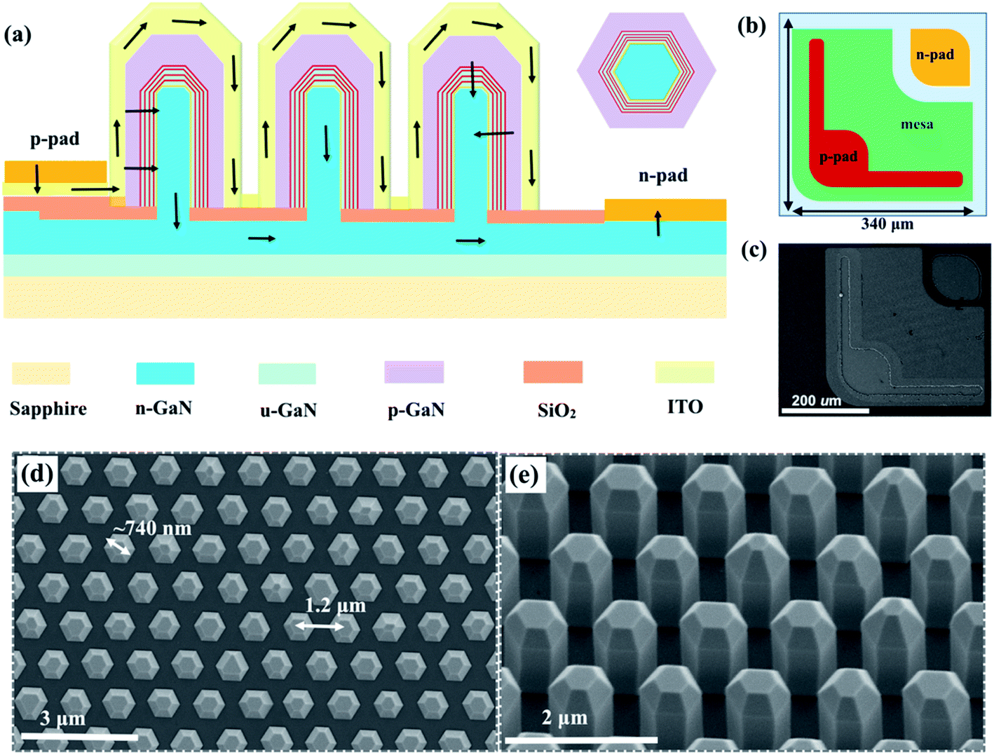 | ||
| Fig. 1 (a) Schematic diagram of the nanowire-based LED device structure. The hexagonal shape of the cross-sectional view of one nanowire is illustrated on the right, involving the n-type core, GaInN/GaN multiple-quantum-shell (MQS) active layer, and p-type GaN shell. (b) The designed LED chip (340 μm × 340 μm), and the corresponding (c) scanning electron microscopy (SEM) image after the process. (d) The planar-view SEM image of an as-grown nanowire sample and (e) the 30°-tilted view SEM image. | ||
3. Results and discussion
3.1 Comparison of EL and CL emission peaks
For sample a, the EL results were compared with the CL spectra obtained from each plane to identify the electronically stimulated emission planes, as shown in Fig. 2. A microprobe setup was employed for EL measurements, while the emitted light was detected from the back side of the chips. In Fig. 2(a), three peaks located at 440, 540, and 630 nm are distinguished in the EL spectra, especially at an injection current higher than 50 mA. At 100 mA, the EL intensity of the longer emission peaks at 540 and 630 nm is approximately two-thirds of that at 440 nm. At a low injection current, EL spectra are dominated by the peak located at 650 nm. Notably, the emission peaks at 440 and 540 nm are invariable with an increase in injection current; however, a slight blueshift is observed for the peak located around 630 nm. Here, it can be inferred that the emission peaks at 440 and 540 nm are mainly from nonpolar and semipolar planes, whereas the peak located around 630 nm is attributable to the non-uniform In-rich clusters or deep-level defects in the polar c-plane region. This is because the growth of MQSs on nanowires mainly depends on the high impinging rate of adatoms, diffusion along the nanowires, and the lateral diffusion from the SiO2 mask layer. The combined effect of these three factors results in a spatial distribution of In incorporation along the nanowires, i.e. a higher In concentration in the c-plane apex region than the r- and m-planes.12,31 The blue shift of the peak near 630 nm is associated with the QCSE of the polar c-plane so that the effective field strength was reduced by the Coulomb screening as the injection current increased.33 On the other hand, such a kind of phenomenon in nanowire-based LEDs was also ascribed to the locally enhanced potential drop near the c-plane region with In fluctuation, especially at a low injection current.12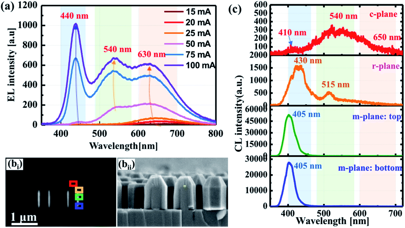 | ||
| Fig. 2 (a) Electroluminescence spectra of sample a at different injection currents. Three peaks located at 440, 540 and 630 nm are identified. (bi) and (bii) The cross-sectional view CL panchromatic mapping and SEM images of the nanowires in sample a. Panels in (c) show the CL spectra acquired in the c-plane apex region, r-plane, and top and bottom areas on the m-plane. | ||
To confirm the EL emission peaks, CL measurements were performed on the m-, r- and c-plane regions across the cleaved GaInN/GaN MQS nanowires. Fig. 2(bi) and (bii) show the CL panchromatic mapping and the corresponding SEM images. The bright light emission in the mapping is related to the coaxial GaInN/GaN MQS layer. However, emission intensity is much weaker at the r- and c-planes. In the CL spectra plotted in Fig. 2(c), a redshift of 25 nm is observed from the bottom part of the m-plane to the r-plane region, which is due to the spatial distribution of In incorporation along the nanowires.32 Specifically, two prominent emission peaks appeared in the r-plane region, indicating the nonuniform In incorporation during growth. In addition, a broad yellowish emission range from 480 to 650 nm is confirmed in the c-plane area, which is attributable to the In-rich clusters and point defect related recombination.34,35 Compared with the EL spectra, CL emission peaks of the m- and r-planes correspond to the EL emission peak at 440 nm, as marked by the rectangle in Fig. 2(a) and (c). On the other hand, the CL spectra of the r- and c-plane indicate that the EL peak at 540 nm is contributed by the emission from both the r- and c-planes, since the In incorporation rate is higher in the apex region as confirmed through energy-dispersive X-ray spectroscopy line-scan profiles of nanowires.30 However, a deviation was confirmed for the peaks at 440 and 405–430 nm in the EL and CL spectra, respectively. This can be attributed to the difference in the characterization methods between injection current through plenty of nanowires in the LED chips and the weak electron beam irradiation on a single nanowire. Despite the In-rich clusters in the c-plane MQS, the deep-level defects such as the Mg–N-vacancy complex and other related point defects are assignable to the red component (∼630 nm) in EL spectra.34 Therefore, the multiple tunneling via defects and In-rich clusters occurred on the c-plane area at a low injection current, resulting in a strong emission located around 630 nm.34,36 Overall, the results here indicate that the EL emission at 440 nm is inevitably from the m- and r-planes, whereas the broad emission at 540 nm originated from both the r- and c-planes. Regarding the EL peak located at 630 nm, it is considered to be from the non-uniform In-rich clusters and deep-level defects in the c-plane MQS. A further investigation of the nanowire growth conditions was conducted to find the origin of multi-color emission in nanowire LEDs.
3.2 Effect of AlGaN spacers on the EL emission wavelength
The crystalline quality of MQSs is critical for high-performance nanowire-based LEDs. As reported, high IQE and high In contents can be simultaneously achieved using an AlGaN spacer before increasing the barrier temperature for MQS growth, since the decomposition of GaInN quantum wells was suppressed on all planes.30 Accordingly, samples b and c were prepared to further verify the effect of AlGaN spacers on the EL emission wavelength. The I–V and EL characteristics of the nanowire devices with and without AlGaN spacers are depicted in Fig. 3(a) and (b). Both samples have current leakage, which is attributed to the unintentional exfoliation of a few nanowires in the mesa area during the fabrication process. Since the growth conditions for the p-GaN shell were identical, the I–V characteristic curves are similar, despite the slightly higher resistance on account of the variation in height. The cross-sectional SEM images of the nanowires in the insets of Fig. 3(a) show an unconformable deposition of the ITO layer on the nanowires, particularly in sample b. The thicknesses of the ITO film on the c- and r-planes are approximately 400 and 270 nm, respectively, whereas only a 30 nm-thick ITO was deposited at the bottom of the m-plane. As a result, such imperfect ITO coverage impeded the spread of current among the nanowires in the mesa area. In addition, the In fluctuation along nanowires may induce current concentration at the upper part of the nanowires in the LEDs. The normalized EL spectra in Fig. 3(b) show that the emission peaks of the LEDs in samples b and c are 430 and 520 nm at the injection current of 100 mA, respectively, which are dominated by the emission from the m- and r-planes. The higher growth temperature of GaN quantum barriers also ensured a singular EL emission in the nanowire LEDs, yielding a narrower full width at half maximum than that of sample a. Moreover, inserting an AlGaN spacer in MQS growth sufficiently increased the In content in GaInN wells, as a 90 nm redshift is observed in sample c. This is attributable to the suppression of the In decomposition rate in the GaInN wells by the AlGaN spacer during ramping up the barrier growth temperature. Such an effect has been demonstrated in the MQS nanowires, which was ascribed to the thermal stability of AlGaN owing to the high sticking coefficient of Al adatoms and large bond energy of Al–N.30,37 This phenomenon was also confirmed in planar c-plane LEDs, allowing high In incorporation into InGaN wells.38,39 Moreover, the yellow-red range emission is negligible in these two samples because of the improved growth of MQSs and p-GaN shell on the c-plane area.41,42 The standard growth of MQSs in sample a can induce indistinguishable MQS structures at the c-plane apex, including non-uniform In-rich clusters.30,40 Thereupon, considerable stacking faults, dislocations, pyramids, or other point defects may be formed in the p-GaN shell of sample a. The improved growth on the c-plane apex was also expected to improve the crystalline quality of p-type GaN at the apex of nanowires in both samples b and c.42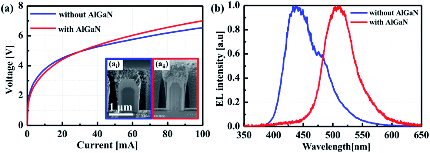 | ||
| Fig. 3 (a) The I–V characteristics of nanowire-LED samples b (without AlGaN spacers) and c (with AlGaN spacers). The cross-sectional view SEM images of sample b (ai) and c (aii) coated with the indium tin oxide film. (b) The normalized EL spectra of samples b and c at an injection current of 100 mA. | ||
3.3 Identification of the red emission component in nanowire LEDs
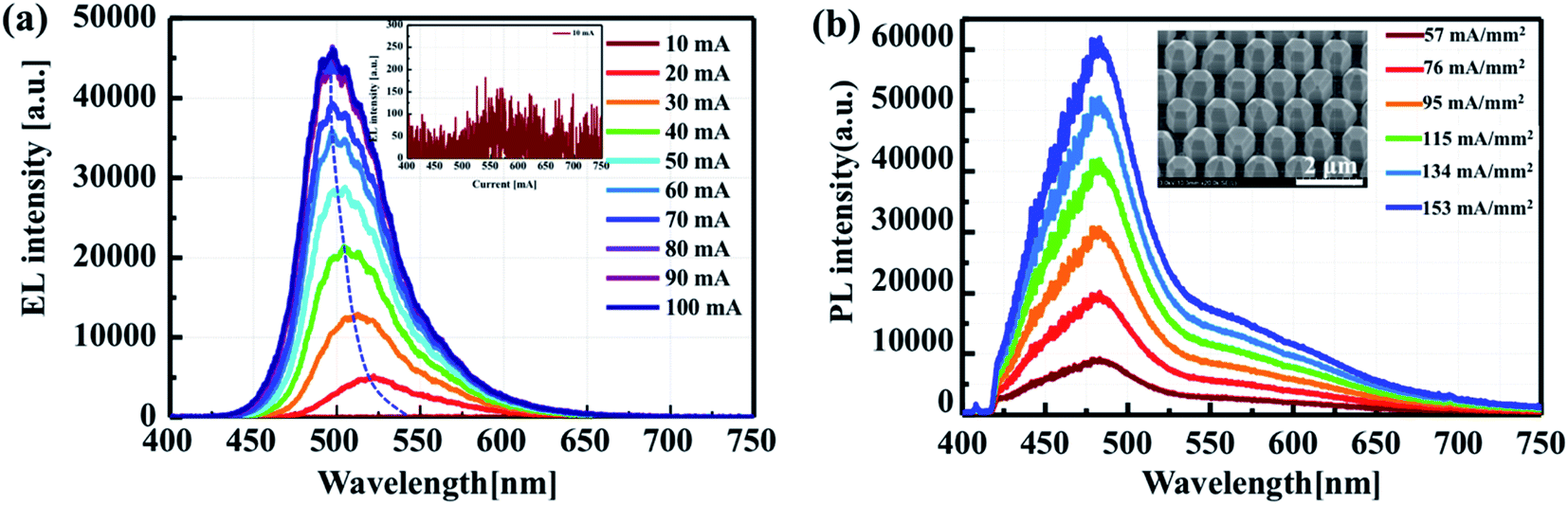
To confirm the effect of activation time on the EL emission wavelength in nanowire LEDs, thermal annealing was performed on sample d (cleaved into two half-sizes: d1 and d2) with different times, 30 and 90 min, respectively. The I–V characteristics, light output characteristics, and optical properties were characterized, as depicted in Fig. 4. For the nanowire LED with 30 min thermal annealing, only one emission peak at 480 nm is observed, as shown in Fig. 4(a). The emission wavelength is stable as a function of injection current, and the peak intensity increased as the current increased. This demonstrates the critical feature of nonpolar/semipolar GaN/GaInN MQSs on nanowires without a clear blueshift induced by the QCSE. Besides the main EL peak at 480 nm, another distinct peak at 630 nm appears in sample d2, as shown in Fig. 4(c). Regarding the two prominent peaks, the shorter one at 480 nm is assumed to be from the MQS active layer, whereas the longer one at 630 nm is related to the emission from defects near the c-plane area.20 Several defects such as various In-rich clusters, point defects, and stacking defects exist near the c-plane of the MQS nanowires, as elaborated in Section 3.1. The insets of Fig. 4(a) and (c) show the emission graphs taken from the front side through a microscope, which was different from the measurement of EL spectra. Nanowire-LED samples d1 and d2 manifest red luminescence over the entire mesa area at low injection current and localized blue dot luminescence with an increase in injection current. However, the emission color of LED figures in sample d2 is dominated by the yellow-red light even at high injection current. Therefore, EL peaks measured from the back side and emission graphs obtained from the front side can initially testify that the yellow-red emission is primarily caused by the presence of considerable In-rich clusters and point defects at the c-plane of the MQS nanowires. Of note, such a phenomenon was aggravated by the concentration of current at the top of the nanowires on account of non-uniform ITO film deposition on the entire nanowires.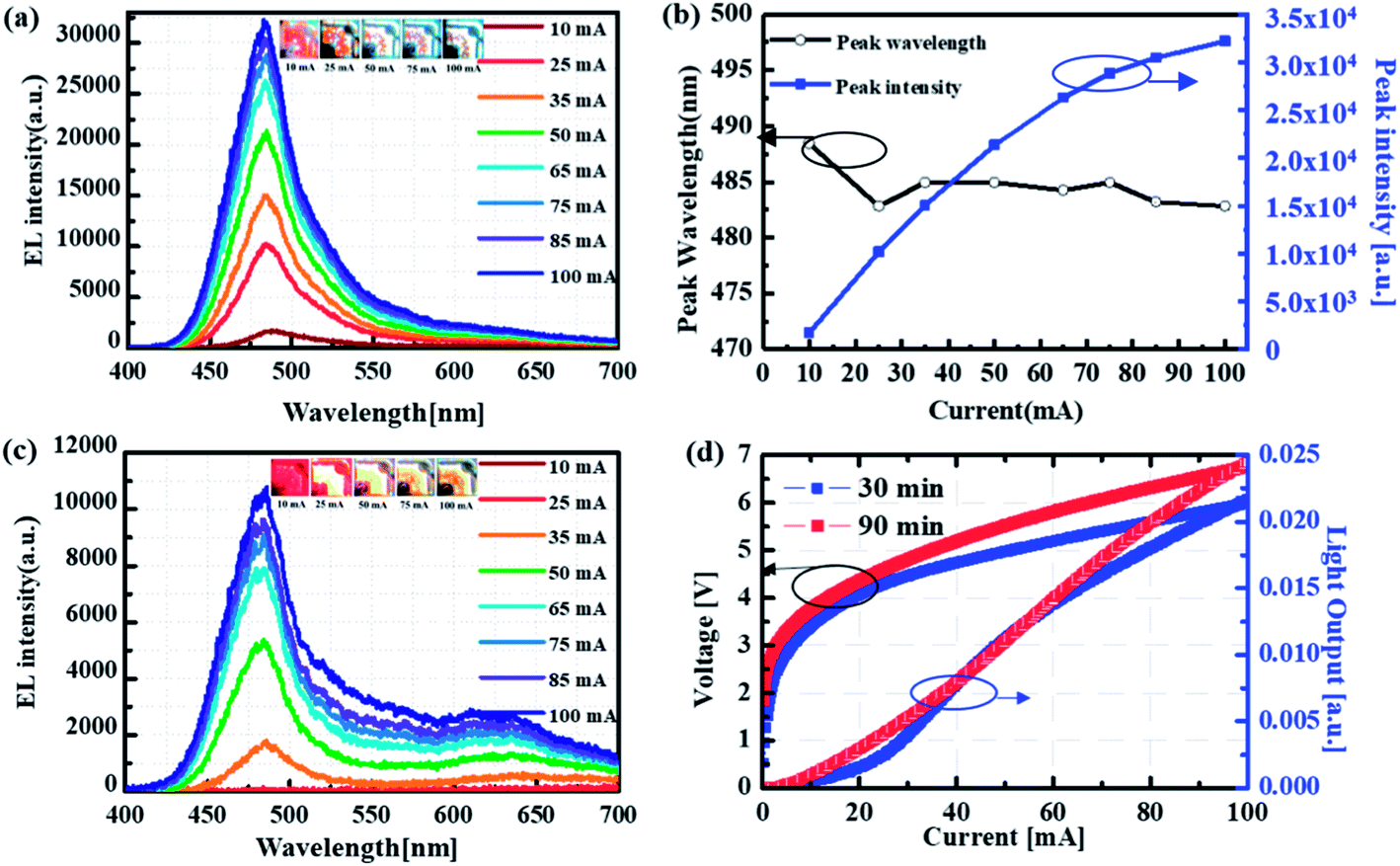 | ||
| Fig. 4 (a) EL spectra of sample d1 with an activation time of 30 min for the p-GaN shell. The corresponding light emission images at different injection currents are shown as insets. (b) The emission peak and intensity as a function of injection current varying from 10 to 100 mA. (c) EL spectra of sample d2 with an activation time of 90 min for the p-GaN shell. (d) The I–V characteristics and light output of sample d with 30 and 90 min activation, respectively. | ||
Furthermore, the EL intensity of the emission peak at 480 nm in LED sample d1 is 2.7 times stronger than that of sample d2. The degradation of the peak at 480 nm is attributable to prolonged annealing, which may be detrimental to the MQS active layer. In contrast, the long emission component at 630 nm is enhanced by approximately four times because of the activation of deep-level defects near the c-plane, which acted as radiative recombination centers. These results indicate that prolonged activation annealing can reduce the intensity of the emission from MQSs and strengthen the red emission from defect levels, which is not suitable for nanowire LEDs. According to the I–V characteristic curves in Fig. 4(d), an increase in differential resistance, as well as a reduced leakage due to prolonged annealing, was confirmed. The I–L characteristics indicate that the light output of sample d1 gradually increased at low injection current and then rapidly increased as the current exceeded 30 mA. On the other hand, for the LEDs that were thermally annealed for 90 min, the light output increased relatively linearly as a function of injection current. Note that the I–L signal was also detected from the back side of the chips as that of EL measurements. The integrated intensity of the EL spectra was verified to be larger in the 90 min thermally annealed LEDs due to the strong emission in the longer wavelength side. Thus, the light output intensity of sample d2 is reasonably stronger than that of sample d1. Although the AlGaN spacer was implied in sample d, the weak yellow-red emission from the c-plane MQS is still observed in the nanowire LEDs. Appropriate activation conditions of p-GaN shells are beneficial to improve electrical properties.
To verify the EL emission peak at 480 nm, sample e was grown under identical conditions to sample d, except for a 10 °C lowered temperature for GaInN quantum wells. Fig. 5 shows the optical characteristics of the LED devices in sample e. In Fig. 5(a), the EL emission peaks show a blueshift from 540 to 500 nm as the injection current increased from 10 to 100 mA. The inset of Fig. 5(a) shows that the EL intensity is extremely low at the injection current of 10 mA. This suggests that the emitted light was mainly from the c-planes at lower injection current, and then shifted to the r- and m-planes as the injection current increased. Nevertheless, in comparison with the EL spectra of the LEDs with GaInN wells grown at 750 °C [see Fig. 4(a)], a redshift from 480 to 500 nm was observed in sample d at the injection current of 100 mA. This is ascribed to the enhanced In incorporation in the GaInN well by lowering the well growth temperature. The emission intensity is also comparable to that of sample d. Therefore, AlGaN spacers and a high barrier growth temperature can be used to effectively achieve high In incorporation in GaInN wells with a lower growth temperature of GaInN wells. To better understand optical performance, power-dependent-PL spectral measurements were performed in the nanowire sample e. An intense emission peak from GaInN/GaN MQSs was observed at 480 nm, as shown in Fig. 5(b). Because the PL signal is detected from the front side of the nanowire arrays, the broadened and blue-shifted emission peak results from the overall emission on the m-, r-, and c-planes of the MQS structures. Specifically, a broad yellow luminescence from In-rich clusters and point defects in the c-plane MQS or near p-GaN shell is also observed. Of note, the EL spectra measured from the back side of the chip are dominated by the emission from the upper part of the nanowire array due to the localized electric field.
 | ||
| Fig. 5 (a) The EL spectra in sample e measured at different injection currents. The inset shows the EL spectrum at an injection current of 10 mA. (b) PL spectra of sample e measured under irradiation using a 405 nm laser with different current intensities. | ||
4. Conclusion
In summary, the optical and electrical properties of coaxial GaInN/GaN MQS nanowire-based LEDs were systematically investigated by varying the growth and activation conditions. EL and CL spectra were recorded for the samples to identify the distinguishable emission peaks in nanowire LEDs. It was inferred that the EL emission peaks (440, 540, and 630 nm) in nanowire LEDs were emitted from the m-planes, r-planes, and the various In-rich clusters, as well as deep-level defect-related centers near the c-planes, respectively. Since the MQS quality is vital for nanowire LEDs, GaN/AlGaN spacers and an increased growth temperature of GaN barriers were applied for the MQS growth. Consequently, the EL spectra of nanowire LEDs exhibited narrowed emission peaks and a clear redshift from 430 nm to 520 nm upon insertion of AlGaN spacers. The redshift was attributed to the suppression of In decomposition from the wells by AlGaN spacers during ramping up of the growth temperature. The absence of a blueshift of the EL emission peaks as a function of the injection current confirms the critical feature of nonpolar GaN/GaInN MQSs on nanowires without the QCSE. A prolonged activation annealing was performed on the nanowire sample to gain insight into the weak emission at 630 nm of nanowire LEDs. Nevertheless, the intensity of the emission from MQSs was decreased, and yielded a four-fold enhancement of the yellow-red emission component. Such a phenomenon was attributed to the activation of deep-level defects in the c-plane MQS, which acted as radiative recombination centers. By changing the growth temperature of the well from 750 °C to 740 °C, a redshift from 480 to 500 nm was observed at 100 mA injection current. This is because the decomposition rate of In in the wells was suppressed by the lower growth temperature of the GaInN wells. Overall, the control of EL emission peaks and the corresponding emission mechanism in this study are quite essential for developing nanowire-based white LEDs and micro-LEDs.Author contributions
W. L. devised the experiments in this work. K. I. fabricated the LED devices, measured the chip performance, and prepared the first draft of the manuscript. W. L. and K. I. prepared all the figures. W. L. grew the nanowire samples, measured the PL spectra, analyzed the results, and re-wrote and revised the manuscript. W. L. prepared the response to reviewers' comments with input from K. I. S. Katsuro contributed to the device fabrication and characterization of samples d and e. N. N. contributed to the epitaxial growth of samples d and e. N. S., K. M., and R. O. supported the epitaxial growth and device fabrication. S. Kamiyama assisted in writing the discussion and revising the manuscript. S. Kamiyama, T. T., M. I., and I. A. contributed to the data analysis and supervised the project.Conflicts of interest
There are no conflicts to declare.Acknowledgements
This work was financially supported by MEXT “Program for research and development of next-generation semiconductor to realize energy-saving society” [No. JPJ005357], MEXT “Private University Research Branding Project”, JSPS KAKENHI for Scientific Research A [No. 15H02019], JSPS KAKENHI for Scientific Research A [No. 17H01055], JSPS KAKENHI for Innovative Areas [No. 16H06416], and Japan Science and Technology CREST [No. 16815710].References
- R.-H. Horng, H.-Y. Chien, F.-G. Tarntair and D.-S. Wuu, Fabrication and Study on Red Light Micro-LED Displays, IEEE J. Electron Devices Soc., 2018, 6, 1064–1069 CAS.
- K. Zhang, D. Peng, K. M. Lau and Z. Liu, Fully-integrated active matrix programmable UV and blue micro-LED display system-on-panel (SoP), J. Soc. Inf. Disp., 2017, 25, 240–248 CrossRef CAS.
- L. Z. Jun, W. K. Ming, K. C. Wing, T. C. Wah and L. K. May, Monolithic LED Microdisplay on Active Matrix Substrate Using Flip-Chip Technology, IEEE J. Sel. Top. Quantum Electron., 2009, 15, 1298–1302 Search PubMed.
- J. Day, J. Li, D. Y. C. Lie, C. Bradford, J. Y. Lin and H. X. Jiang, III-Nitride full-scale high-resolution microdisplays, Appl. Phys. Lett., 2011, 99, 031116 CrossRef.
- A. Paranjpe, J. Montgomery, S. M. Lee and C. Morath, Micro-LED Displays: Key Manufacturing Challenges and Solutions, SID Symposium Digest of Technical Papers, Wiley Online Library, 2018, pp. 597–600 Search PubMed.
- H. Jiang and J. Lin, Nitride micro-LEDs and beyond-a decade progress review, Opt. Express, 2013, 21, A475–A484 CrossRef CAS PubMed.
- W. C. Chong, W. K. Cho, Z. J. Liu, C. H. Wang and K. M. Lau, 1700 Pixels Per Inch (PPI) Passive-Matrix Micro-LED Display Powered by ASIC, 2014 IEEE Compound Semiconductor Integrated Circuit Symposium (CSICS), IEEE, 2014, pp. 1–4 Search PubMed.
- I. Akasaki, Nobel lecture: fascinated journeys into blue light, Rev. Mod. Phys., 2015, 87, 1119 CrossRef.
- S. Nakamura, M. Senoh, N. Iwasa and S.-i. Nagahama, High-brightness InGaN blue, green and yellow light-emitting diodes with quantum well structures, Jpn. J. Appl. Phys., 1995, 34, L797 CrossRef CAS.
- T. Takeuchi, S. Sota, M. Katsuragawa, M. Komori, H. Takeuchi, H. Amano and I. Akasaki, Quantum-confined Stark effect due to piezoelectric fields in GaInN strained quantum wells, Jpn. J. Appl. Phys., 1997, 36, L382 CrossRef CAS.
- T. Takeuchi, C. Wetzel, S. Yamaguchi, H. Sakai, H. Amano, I. Akasaki, Y. Kaneko, S. Nakagawa, Y. Yamaoka and N. Yamada, Determination of piezoelectric fields in strained GaInN quantum wells using the quantum-confined Stark effect, Appl. Phys. Lett., 1998, 73, 1691–1693 CrossRef CAS.
- Y. J. Hong, C. H. Lee, A. Yoon, M. Kim, H. K. Seong, H. J. Chung, C. Sone, Y. J. Park and G. C. Yi, Visible-color-tunable light-emitting diodes, Adv. Mater., 2011, 23, 3284–3288 CrossRef CAS.
- J. Y. Lin and H. X. Jiang, Development of microLED, Appl. Phys. Lett., 2020, 116, 100502 CrossRef CAS.
- T. W. Yeh, Y. T. Lin, L. S. Stewart, P. D. Dapkus, R. Sarkissian, J. D. O'Brien, B. Ahn and S. R. Nutt, InGaN/GaN multiple quantum wells grown on nonpolar facets of vertical GaN nanorod arrays, Nano Lett., 2012, 12, 3257–3262 CrossRef CAS.
- S. Kamiyama, W. Lu, T. Takeuchi, M. Iwaya and I. Akasaki, Growth and Characterization of Core-Shell Structures Consisting of GaN Nanowire Core and GaInN/GaN Multi-Quantum Shell, ECS J. Solid State Sci. Technol., 2019, 9, 015007 CrossRef.
- K. Ito, W. Lu, N. Sone, Y. Miyamoto, R. Okuda, M. Iwaya, T. Tekeuchi, S. Kamiyama and I. Akasaki, Development of Monolithically Grown Coaxial GaInN/GaN Multiple Quantum Shell Nanowires by MOCVD, Nanomaterials, 2020, 10, 1354 CrossRef CAS PubMed.
- H. Sekiguchi, K. Kishino and A. Kikuchi, Emission color control from blue to red with nanocolumn diameter of InGaN/GaN nanocolumn arrays grown on same substrate, Appl. Phys. Lett., 2010, 96, 231104 CrossRef.
- K. Kishino, K. Nagashima and K. Yamano, Monolithic integration of InGaN-based nanocolumn light-emitting diodes with different emission colors, Appl. Phys. Express, 2012, 6, 012101 CrossRef.
- W. Lu, K. Ito, N. Sone, R. Okuda, Y. Miyamoto, M. Iwaya, T. Tekeuchi, S. Kamiyama and I. Akasaki, Color-tunable emission in coaxial GaInN/GaN multiple quantum shells grown on three-dimensional nanostructures, Appl. Surf. Sci., 2021, 539, 148279 CrossRef CAS.
- E. A. Evropeitsev, D. R. Kazanov, Y. Robin, A. N. Smirnov, I. A. Eliseyev, V. Y. Davydov, A. A. Toropov, S. Nitta, T. V. Shubina and H. Amano, State-of-the-art and prospects for intense red radiation from core–shell InGaN/GaN nanorods, Sci. Rep., 2020, 10, 190480 Search PubMed.
- Y.-S. Chen, W.-Y. Shiao, T.-Y. Tang, W.-M. Chang, C.-H. Liao, C.-H. Lin, K.-C. Shen, C. Yang, M.-C. Hsu and J.-H. Yeh, Threading dislocation evolution in patterned GaN nanocolumn growth and coalescence overgrowth, J. Appl. Phys., 2009, 106, 023521 CrossRef.
- K. Kishino and S. Ishizawa, Selective-area growth of GaN nanocolumns on Si (111) substrates for application to nanocolumn emitters with systematic analysis of dislocation filtering effect of nanocolumns, Nanotechnology, 2015, 26, 225602 CrossRef PubMed.
- T.-Y. Tang, W.-Y. Shiao, C.-H. Lin, K.-C. Shen, J.-J. Huang, S.-Y. Ting, T.-C. Liu, C. Yang, C.-L. Yao and J.-H. Yeh, Coalescence overgrowth of GaN nanocolumns on sapphire with patterned metal organic vapor phase epitaxy, J. Appl. Phys., 2009, 105, 023501 CrossRef.
- W. Bergbauer, M. Strassburg, C. Kölper, N. Linder, C. Roder, J. Lähnemann, A. Trampert, S. Fündling, S. Li and H. Wehmann, Continuous-flux MOVPE growth of position-controlled N-face GaN nanorods and embedded InGaN quantum wells, Nanotechnology, 2010, 21, 305201 CrossRef CAS.
- M. Tchernycheva, C. Sartel, G. Cirlin, L. Travers, G. Patriarche, J. Harmand, L. S. Dang, J. Renard, B. Gayral and L. Nevou, Growth of GaN free-standing nanowires by plasma-assisted molecular beam epitaxy: structural and optical characterization, Nanotechnology, 2007, 18, 385306 CrossRef.
- M. Nami, I. E. Stricklin, K. M. DaVico, S. Mishkat-Ul-Masabih, A. K. Rishinaramangalam, S. Brueck, I. Brener and D. F. Feezell, Carrier dynamics and electro-optical characterization of high-performance GaN/InGaN core-shell nanowire light-emitting diodes, Sci. Rep., 2018, 8, 1–11 CAS.
- G. Cossu, A. Khalid, P. Choudhury, R. Corsini and E. Ciaramella, 3.4 Gbit/s visible optical wireless transmission based on RGB LED, Opt. Express, 2012, 20, B501–B506 CrossRef CAS.
- M. Nami, A. Rashidi, M. Monavarian, S. Mishkat-Ul-Masabih, A. K. Rishinaramangalam, S. R. Brueck and D. Feezell, Electrically Injected GHz-Class GaN/InGaN Core–Shell Nanowire-Based μLEDs: Carrier Dynamics and Nanoscale Homogeneity, ACS Photonics, 2019, 6, 1618–1625 CrossRef CAS.
- Y. H. Ra and C. R. Lee, Core-Shell Tunnel Junction Nanowire White-Light-Emitting Diode, Nano Lett., 2020, 20, 4162–4168 CrossRef CAS PubMed.
- W. Lu, Y. Miyamoto, R. Okuda, K. Ito, N. Sone, M. Iwaya, T. Tekeuchi, S. Kamiyama and I. Akasaki, Correlation between Optical and Structural Characteristics in Coaxial GaInN/GaN Multiple Quantum Shell Nanowires with AlGaN Spacers, ACS Appl. Mater. Interfaces, 2020, 12, 51082–51091 CrossRef CAS.
- Y. Robin, S. Y. Bae, T. V. Shubina, M. Pristovsek, E. A. Evropeitsev, D. A. Kirilenko, V. Y. Davydov, A. N. Smirnov, A. A. Toropov, V. N. Jmerik, M. Kushimoto, S. Nitta, S. V. Ivanov and H. Amano, Insight into the performance of multi-color InGaN/GaN nanorod light emitting diodes, Sci. Rep., 2018, 8, 7311 CrossRef CAS PubMed.
- W. Lu, N. Sone, N. Goto, K. Iida, A. Suzuki, D. P. Han, M. Iwaya, T. Tekeuchi, S. Kamiyama and I. Akasaki, Effect of AlGaN undershell on the cathodoluminescence properties of coaxial GaInN/GaN multiple-quantum-shells nanowires, Nanoscale, 2019, 11, 18746–18757 RSC.
- S. F. Chichibu, A. Uedono, T. Onuma, B. A. Haskell, A. Chakraborty, T. Koyama, P. T. Fini, S. Keller, S. P. Denbaars, J. S. Speck, U. K. Mishra, S. Nakamura, S. Yamaguchi, S. Kamiyama, H. Amano, I. Akasaki, J. Han and T. Sota, Origin of defect-insensitive emission probability in In-containing (Al,In,Ga)N alloy semiconductors, Nat. Mater., 2006, 5, 810–816 CrossRef CAS PubMed.
- Q. Yan, A. Janotti, M. Scheffler and C. G. Van de Walle, Role of nitrogen vacancies in the luminescence of Mg-doped GaN, Appl. Phys. Lett., 2012, 100, 142110 CrossRef.
- J. L. Lyons, A. Janotti and C. G. Van de Walle, Carbon impurities and the yellow luminescence in GaN, Appl. Phys. Lett., 2010, 97, 152108 CrossRef.
- Y. Huang, F. Yun, Y. Li, W. Ding, Y. Wang, H. Wang, W. Zhang, Y. Zhang, M. Guo, S. Liu and X. Hou, Defect-induced color-tunable monolithic GaN-based light-emitting diodes, Appl. Phys. Express, 2014, 7, 102102 CrossRef.
- M. Albrecht, L. Lymperakis, J. Neugebauer, J. E. Northrup, L. Kirste, M. Leroux, I. Grzegory, S. Porowski and H. P. Strunk, Chemically orderedAlxGa1−xNalloys: Spontaneous formation of natural quantum wells, Phys. Rev. B: Condens. Matter Mater. Phys., 2005, 71, 035314 CrossRef.
- S. Hussain, K. Lekhal, H. Kim-Chauveau, P. Vennéguès, P. De Mierry and B. Damilano, Capping green emitting (Ga,In)N quantum wells with (Al,Ga)N: impact on structural and optical properties, Semicond. Sci. Technol., 2014, 29, 035016 CrossRef CAS.
- D. Koleske, A. Fischer, B. Bryant, P. Kotula and J. Wierer, On the increased efficiency in InGaN-based multiple quantum wells emitting at 530–590 nm with AlGaN interlayers, J. Cryst. Growth, 2015, 415, 57–64 CrossRef CAS.
- W. Lu, N. Goto, H. Murakami, N. Sone, K. Iida, M. Terazawa, D.-P. Han, M. Iwaya, T. Tekeuchi, S. Kamiyama and I. Akasaki, Controlled synthesis of nonpolar GaInN/GaN multiple-quantum-shells on GaN nanowires by metal-organic chemical vapour deposition, Appl. Surf. Sci., 2020, 509, 145271 CrossRef CAS.
- S. Katsuro, W. Lu, K. Ito, N. Nakayama, N. Sone, K. Okuno, M. Iwaya, T. Takeuchi, S. Kamiyama and I. Akasaki, Emission characteristics of GaInN/GaN multiple quantum shell nanowire-based LEDs with different p-GaN growth conditions, Nanophotonics, 2021, 10, 3441–3450 CrossRef.
- W. Lu, N. Nakayama, K. Ito, S. Katsuro, N. Sone, Y. Miyamoto, K. Okuno, M. Iwaya, T. Takeuchi, S. Kamiyama and I. Akasaki, Morphology Control and Crystalline Quality of p-Type GaN Shells Grown on Coaxial GaInN/GaN Multiple Quantum Shell Nanowires, ACS Appl. Mater. Interfaces, 2021 DOI:10.1021/acsami.1c13947.
Footnote |
| † These authors contributed equally to this work. |
| This journal is © The Royal Society of Chemistry 2022 |