
 Open Access Article
 This Open Access Article is licensed under a
 Creative Commons Attribution 3.0 Unported Licence
Control of up-to-down/down-to-up light-induced ferroelectric polarization reversal†
Huan
Tan
 a,
Gustavo
Castro
b,
Jike
Lyu
a,
Pablo
Loza-Alvarez
b,
Florencio
Sánchez
a,
Josep
Fontcuberta
a and
Ignasi
Fina
*a
a,
Gustavo
Castro
b,
Jike
Lyu
a,
Pablo
Loza-Alvarez
b,
Florencio
Sánchez
a,
Josep
Fontcuberta
a and
Ignasi
Fina
*a
aInstitut de Ciència de Materials de Barcelona (ICMAB-CSIC), Campus UAB, Bellaterra, 08193, Barcelona, Spain. E-mail: ifina@icmab.es
bICFO-Institut de Ciencies Fotoniques, The Barcelona Institute of Science and Technology, 08860, Castelldefels, Barcelona, Spain
First published on 4th August 2022
Abstract
Light control of ferroelectric polarization is of interest for the exploitation of ferroelectric thin films in ultrafast data storage and logic functionalities. The rapidly oscillating electric field of light absorbed in a ferroelectric layer can suppress its polarization but cannot selectively reverse its direction. Here we take advantage of the built-in asymmetry at ferroelectric/electrode interfaces to break the up/down symmetry in uniaxial ferroelectrics to promote polarization reversal under illumination. It is shown that appropriate ferroelectric/metal structures allow the direction of the imprint electric field to be selected, which is instrumental for polarization reversal. This ability is further exploited by demonstrating the optical control of the resistance states in a ferroelectric capacitor.
New conceptsFerroelectric materials are fascinating and useful because they show spontaneous electric polarization and it is strongly coupled to long-range electric and stress fields. Piezoelectricity and electrically switchable polarization arise from these coupled magnitudes. Alternatively, optical control of ferroelectric polarization is of interest for new envisaged devices integrating optical sensing, logic and memory functionalities. The fact is that light is coupled to ferroelectric polarization. However, light cannot univocally determine the final polarization sign and therefore subsidiary tools are needed to unbalance one of the degenerated polarization states. In this communication, we evidence that light can selectively produce up-to-down or down-to-up polarization switching by manipulation of the internal electric field's sign and magnitude. Remarkably, the final polarization state remains after optical stimuli. This method consists in the unbalancing of the internal electric fields, and therefore ferroelectric polarization final state, by appropriate electrode selection. The significance of the developed method combining a photoelectric response and manipulation of internal electric fields has been proven useful in devices with capacitator structures, where resistance can be also selectively switched high-to-low or low-to-high by light. |
Introduction
The light control of memory elements holds promise for energy efficient and ultrafast managing of data storage and computing.1 Moreover, such optically active elements would allow the development of devices combining memory and optical sensing functionalities.2 Among photoresponsive materials, ferroelectrics are particularly interesting as ferroelectric polarization (P) is a non-volatile magnitude, thus providing an intrinsic memory functionality. Therefore, the coupling of photoresponsivity and polarization retention offers new opportunities. For instance, the photovoltaic response of a ferroelectric device can be modulated by the direction of the P.3–5 Besides, the resistance state of ferroelectric tunnel junctions or field effect transistors can be modulated by the electrically-controlled polarization state of the ferroelectric layer.6,7 Therefore, ferroelectric materials offer the opportunity to integrate optically commanded memory functions without relying on voltage-control.8Of relevance here are the coupling mechanisms between light and polarization, which depend on materials and arrangements. Optical absorption in ferroelectrics leads to the modification of its crystal lattice due to the combination of photogalvanic and piezoelectric/electrostrictive effects,9 which may result in modification of its polarization state.10–14 On the other hand, when using semiconducting electrodes in ferroelectric devices, photoabsorption at electrodes allows modulation of the amount of screening charges and consequently of the depolarization field, which can lead to polarization reversal.15 Similar mechanisms have been recently exploited to irreversibly control the polarization state in ferroelectric/2D-semiconductor devices, with the 2D material acting as a photoabsorbing electrode,16 and allowing the observation of the change of resistance state across the devices.16–19 The light can also be absorbed at the interface in metal/ferroelectric capacitor structures, such as in Pb(Zr0.2Ti0.8)O3/La0.7Sr0.3MnO3, where an important role of the film surface morphology on photo-induced polarization reversal was identified.20 On the other hand, ferroelectric materials such as BaTiO3(BTO), PZT, LiNbO3, etc., often present very reactive surfaces and a polarization selective photocatalytic response.21 Concomitantly, polarization can also be affected by the photoinduced changes of surface state, which largely affect the internal field.21–25 These potentially coexisting and entangled mechanisms challenge the fine control of ferroelectric polarization under illumination. Achieving the reversible rotation of the polarization sign by light using the listed mechanisms is not possible. So far, light-induced reversible control of ferroelectric polarization has only been reported in complex ferroelectric devices by exploiting the unconventional bulk photovoltaic response.26,27 Establishing the role of the different intrinsic electric fields of ferroelectric materials, such as the depolarization electric field and imprint electric field, is necessary for device development. Precisely, for applications, it is necessary to fully control the final P state after illumination, which has not been achieved hitherto, and only a detailed analysis of the role of internal electric fields can permit it.
Here we show that the electric imprint field (Eimp) can be tailored by the use of suitable bottom electrodes, and this allows up-to-down or down-to-up polarization switching by illumination. We investigate films of the seemingly best-known ferroelectric material (BaTiO3, BTO). We demonstrate that in films showing Eimp, polarization switching by light can be observed with the final polarization direction dictated by Eimp. Consistently, we also show that when the imprint is absent (Eimp ≈ 0), photoabsorption does not affect the polarization state of the ferroelectric layer. Piezoelectric force microscopy (PFM) provides the first hint at the observed phenomena. Second harmonic generation (SHG) imaging provides a deeper insight into its origin, confirming that photoabsorption at the bulk of the ferroelectric film rules the observed effect rather than changes in the surface state. Finally, we show the robustness of the effect in a metal–ferroelectric–metal device structure, where depending on Eimp, its resistance state can be switched from high-to-low or from low-to-high after suitable illumination.
Results
Epitaxial BTO films of an identical thickness (65 nm) are grown on different single or bilayer epitaxial bottom electrodes on LaAlO3(001) (LAO) substrates. The structures are: BTO/La2/3Sr1/3MnO3 (LSMO)/LaNiO3 (LNO)//LAO, BTO/LNO//LAO, and BTO/SrRuO3 (SRO)/LNO//LAO, as sketched in Fig. 1(a–c). The thickness of the LSMO, LNO and SRO electrodes is 25, 30 and 30 nm, respectively. Note that in the three samples, LNO is grown directly on the LAO substrate, while the LSMO, LNO or SRO layers are in direct contact with the BTO layer. In the following we will refer to the three samples as BTO/LSMO, BTO/LNO and BTO/SRO, respectively. Experimental details on the grown conditions can be found in the methods section and elsewhere.28,29 The use of the same bottom LNO buffer layer allows obtaining BTO layers with similar strain state as demonstrated as follows. In Fig. 1(a–c), we show the X-ray diffraction (XRD) reciprocal space maps (RSMs) of the BTO/LNO, BTO/LSMO and BTO/SRO samples around the (103) reflection of LAO. It can be observed that the (103) reflection of LSMO, LNO and SRO is close to the corresponding reflection from the substrate. The lattice parameters of the layers are indicated in Table S1, ESI.† It can be seen that LNO and LSMO are strained, but SRO is relaxed. The (103) reflection of BTO occurs at a very similar position in the three samples, indicating that the three BTO films have close in-plane and out-of-plane cell parameters. In Fig. 1(a–c), the position of the red cross indicates the peak position of BTO for the BTO/LSMO sample, which as shown, closely coincides with the BTO peak position in the RSM of the BTO/LNO and BTO/SRO samples. The a and c parameters of BTO in the three samples are indicated in Table S1, ESI.† It is seen that both the a and c parameter are expanded with respect to the bulk values. The expansion, usual in epitaxial BTO films grown by pulsed laser deposition, is likely due to oxygen vacancies and other point defects.30 The corresponding XRD specular θ–2θ scans (Fig. S1, ESI†) confirm that BTO films are (001) oriented and that no other crystal orientations or phases are observed. We also conclude that although different layers are used as bottom electrodes, the unit cell parameters of the top BTO films in these three samples are very similar.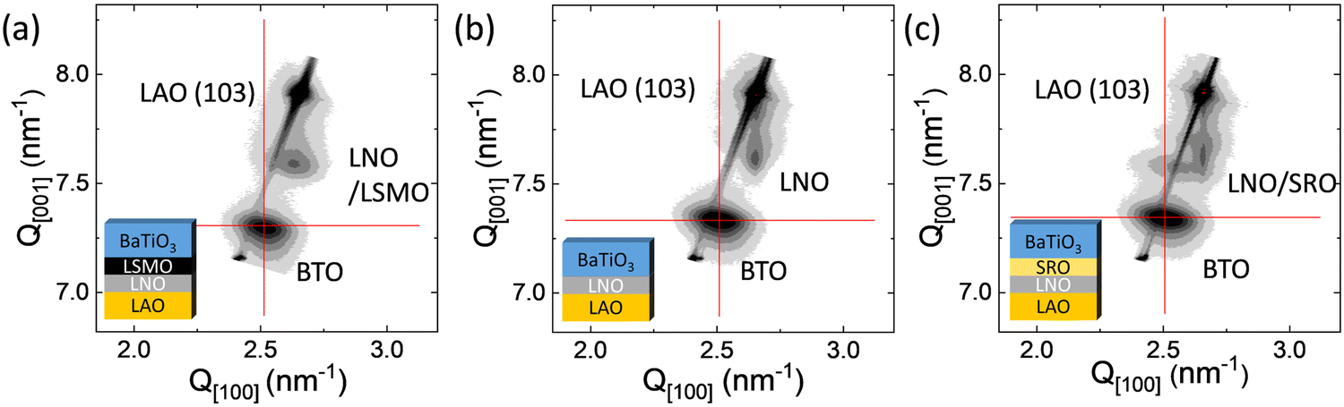 | ||
| Fig. 1 Reciprocal space maps for the BTO/LSMO (a), BTO/LNO (b) and BTO/SRO (c) samples around the LAO (103) reflection. | ||
Next, we analyze the Eimp field of these samples by PFM. The PFM phase loops, Fig. 2(a–c), display the 180° phase contrast typically taken as a signature of the ferroelectric character of the material. Macroscopic characterization also evidences the ferroelectric nature of the three samples (Fig. S2, ESI†). Of interest here is the horizontal shift, which is a fingerprint of Eimp. It can be appreciated that the loop of the BTO/LSMO sample [Fig. 2(a)] is shifted towards the right (V > 0), signaling that Eimp favors the up polarization (Eimp > 0). In contrast, the loop of the BTO/SRO sample [Fig. 2(c)] shows a clear left shift, which indicates that Eimp favors down polarization (Eimp < 0). For the BTO/LNO sample, the loop [Fig. 2(b)] shows only a small shift towards the left, suggesting a very small imprint. The Eimp values are: 178.5, −29.2 and −167.7 kV cm−1 for BTO/LSMO, BTO/LNO and BTO/SRO, respectively. The PFM amplitude loops [Fig. 2(d–f)] have the butterfly shape expected for an intrinsic ferroelectric response and indicate an Eimp direction which is in agreement with that observed in the phase loops. Therefore, it is concluded that the selection of the bottom electrode allows the selection of the presence of the imprint field and its direction in the BTO layer. Several effects can rule the observed variation of the Eimp among samples. Flexoelectric effects resulting from strain gradients,31 asymmetric defect distribution,32 or the combination of them33,34 occurring at the ferroelectric layer might modulate internal electric fields. However, given the very similar lattice parameters of the three samples (Fig. 1), important differences in strain gradients or defect presence can be ruled out. Thus, flexoelectricity or asymmetric defect distribution are not the main mechanisms governing the observed change of sign of the internal electric field, although these might be present, and the role of the selected electrode must be considered. Electrode termination35 can determine Eimp. However, substrates have not been treated so the electrode surface charge is expected to be mixed in LSMO and neutral in LNO and SRO, disregarding a significant change on the charged terminations of the bottom electrodes among samples. Therefore, the different chemistry at the electrode/ferroelectric interface or the different electrostatic boundary conditions imposed by the different electronic properties of the used electrodes are both possible mechanisms determining Eimp. The three used bottom electrodes have similar workfunction 4.9, 4.9, and 5.2 eV for LSMO,36 LNO37 and SRO,38 respectively, which are smaller than Pt (5.7 eV).39 Therefore, the different electrostatic boundary conditions among samples should not be critical for Eimp. Instead, the different particular chemistry at the electrode/ferroelectric interface can be at the origin of the observed Eimp change of sign. Besides, the chemistry at the electrode/ferroelectric interface can also be relevant to determine the type and number of defects, which might potentially also determine sub-bandgap light absorption.
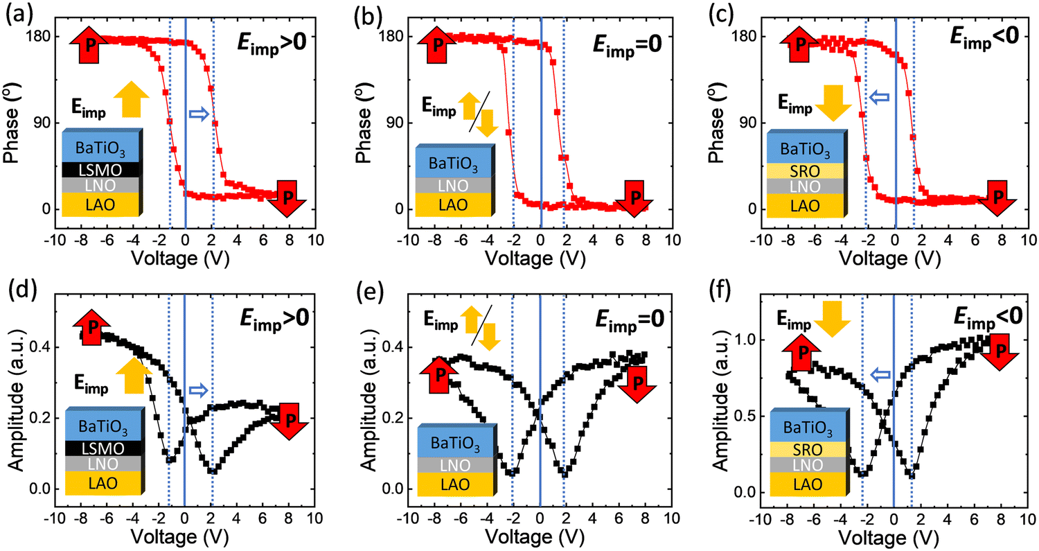 | ||
| Fig. 2 (a–c) PFM phase and amplitude (d–f) loops of the BTO/LSMO, BTO/LNO and BTO/SRO samples, respectively. Sketches of the Eimp direction are indicated by vertical (yellow) and horizontal (open blue) arrows. | ||
Next, we turn to the optical switching of ferroelectric polarization and its relation with the imprint. In Fig. 3(a–c), we show the PFM phase images of the BTO/LSMO, BTO/LNO and BTO/SRO samples, collected after applying either +8 V (dark) or −8 V (bright) to write regions with a well defined polarization. The corresponding PFM amplitude images (Fig. S3, ESI†) show 180° phase contrast between different regions. In the outer region, no voltage has been applied and it corresponds to the pristine polarization state of the BTO film. It can be appreciated in Fig. 3(a) that the outer region of the BTO/LSMO sample is bright. Thus, the as-grown polarization state for the BTO/LSMO sample is up. High temperature retention experiments show that PFM contrast is similar after heating the sample for 10 min and 80 °C (Fig. S4, ESI†), an indication of the good retention of polarization, and therefore the negligible role of depolarization electric field in the reported optical polarization switch. On the contrary, for BTO/LNO and BTO/SRO samples, the contrast in the outermost region is mixed and dark, respectively. Thus, the as-grown polarization state corresponds to a mixture of up and down domains for the BTO/LNO sample but to down polarization for the BTO/SRO. Therefore, it is concluded that the bottom electrode rules the Eimp direction, and Eimp governs the as-grown state polarization, as commonly found in ferroelectric thin films.40
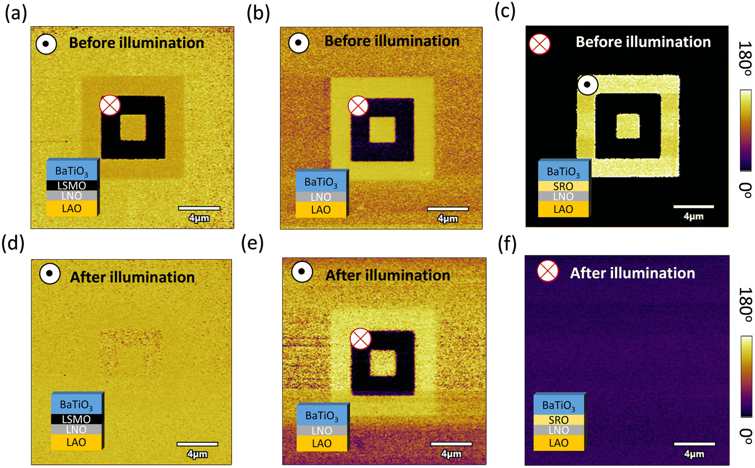 | ||
| Fig. 3 PFM phase images collected (a–c) before and (d–f) after illumination for the BTO/LSMO, BTO/LNO and BTO/SRO samples, respectively. | ||
In Fig. 3(d–f), we show the PFM phase images collected after illumination (405 nm, 12.2 W cm−2, 10 min). Note that the used photons (3.06 eV) are of sub-bandgap energy (Eg = 3.3 eV for BTO).41 It is known that oxygen deficiencies (or other point defects) in BTO introduce donor states, either shallow or deep42 and thus a significant photon absorption for sub-bandgap incoming photons is expected.43 Focusing first on BTO/LSMO, comparison of the images in Fig. 3a and d, reveals that illumination promotes the switching of dark regions to bright indicating that the polarization is optically reversed from down to up. It can also be appreciated that bright regions with up polarization do not suffer any change of contrast. Thus, in the BTO/LSMO sample the as-grown state (polarization up) is recovered after illumination. Note that the sample conductivity increase under illumination is much smaller than that produced by heating the sample up to 40 °C, disregarding the presence of sample heating (Fig. S5, ESI†). For the BTO/LNO, comparison of the images collected before and after illumination states [Fig. 3(b and e)] does not show any appreciable change of contrast. On the contrary, in BTO/SRO [Fig. 3(c and f)], and opposed to BTO/LSMO, the illumination reverses the polarization from up to down, indicating that in the BTO/SRO sample, the as-grown state is also recovered after illumination. Similar optical switching of polarization is observed in BiFeO3 (BFO) films (Fig. S6, ESI†). Absence of optical switching has been observed in the BTO/LSMO and BTO/SRO samples under red illumination using the same power (Fig. S7 and S8, ESI†) and while probing regions near the illuminated area (Fig. S9 and S10, ESI†), further disregarding the important contribution of heating effects and indicating that the polarization switch is driven by photocarrier generation as claimed in previous works.44 In addition, the absence of switching under red illumination in the BTO/LSMO and BTO/SRO samples also indicates that the light absorption and concomitant photocharge generation at the electrode, which should occur at this wavelength, because the LSMO and SRO bandgaps are smaller (Eg,SRO = 0.27 eV45 and Eg,LSMO = 0.63 eV46) than the energy of the red photons (Ered = 1.94 eV), does not have an impact on the P switch under illumination. Therefore, photocarriers generated at the BTO layer are at the origin of the P switch under illumination. In particular, the amplitude of the polarization of a ferroelectric semiconductor shall depend on the amount of available free charges.47 Photogenerated carriers, here generated at BTO as mentioned, can screen ionic charges and eventually cancel the coulomb interaction between them. As a consequence, polarization vanishes. Alternatively, photogenerated carriers can help to screen polarization, thus enhancing it, but cancelling the interaction of internal electric fields with polarization.48 In both cases, the polarization is unstable under illumination and the subsequent reduction of available photocarriers when the light stimulus is off results in the alignment of the ferroelectric polarization with the internal electric fields.44
The PFM measurements described above provide rather compelling evidence that illumination promotes the reversal of the ferroelectric polarization direction at the BTO film surface. However, it would be reassuring to use an additional probe directly related to the ferroelectric polarization of the ferroelectric layer. This is the purpose of the second harmonic generation (SHG) microscopy experiments described in the following. SHG is primarily insensitive to the presence and nature of surface charges and the SHG signal genuinely develops in non-centrosymmetric materials and allows mapping polar domains in ferroelectric materials.49Fig. 4(a) displays the sketch of the experimental set-up. The incident light impinges the film at an angle θ (=17°) with respect to the normal of the film (i.e. the polar c-axis of BTO). In this configuration, in a ferroelectric material with polarization along the normal direction, such as in the BTO films, the intensity of the SHG reflected beam shall depend on the polarization state (up/down) of the material under the field-of-view.49 In Fig. 4(b, left), an SHG map collected on the BTO surface of the BTO/LSMO sample is shown. The sample is previously prepoled using either +8V (dark) or −8 V (bright) using PFM, thus using the same method to that used to collect the images of Fig. 3(a) described above, despite the patterned region is here larger to allow easier localization. Prepoled regions with V+ and V− voltages show an obvious SHG contrast indicating different polarization directions: point up in the bright regions and down in the dark ones. The SHG images collected after illuminating the sample (405 nm, 12.2 W cm−2) (Fig. 4(b), right), show that regions of dark contrast have disappeared, indicating down-to-up optically induced switching. Fig. 4(c) displays the corresponding SHG images collected before (left) and after (right) illuminating the BTO/LNO sample; it can be inferred that light does not change the polarization state of this sample. Finally, Fig. 4(d) displays the SHG images of BTO/SRO. It can be appreciated that bright regions (poled with V−) turn dark after illumination, thus indicating up-to-down polarization reversal. In Fig. 4(d) large dots of bright contrast are observed due to the higher level of surface adsorbates in this sample. Overall, the data in Fig. 4(b–d) show that the contrast changes observed by SHG and PFM before and after illumination are closely coincident. These data confirm that the optical switching of the polarization observed by PFM reflects the switching of the bulk ferroelectric polarization of the BTO layer, rather than non-ferroelectric surface charge or charge injection effects.49
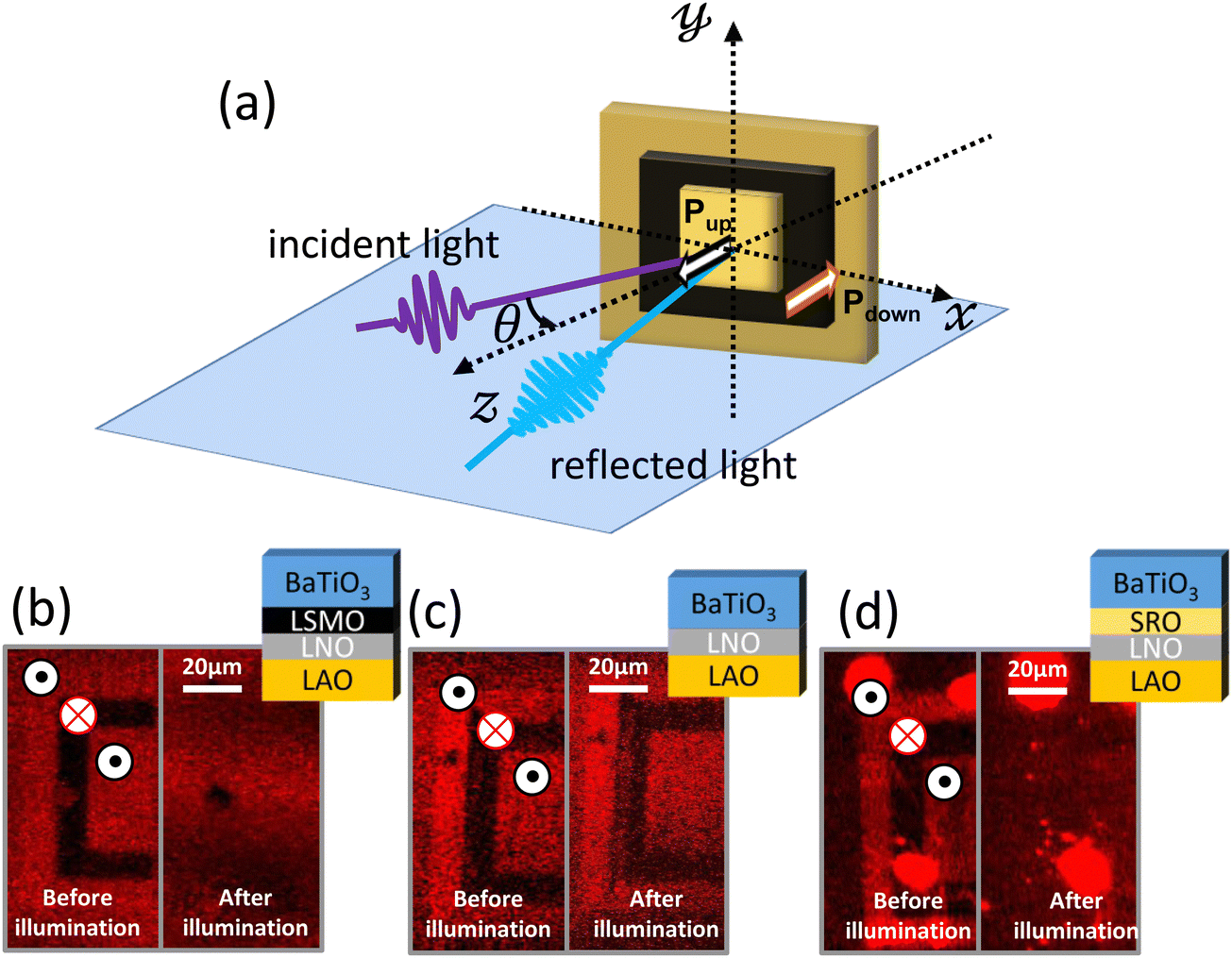 | ||
| Fig. 4 (a) Sketch of the SHG measurements. The Pup and Pdown directions are indicated by the corresponding arrows. (b–d) SHG images after electrical writing (left) and after electrical writing and illumination (right) for the BTO/LSMO, BTO/LNO and BTO/SRO samples, respectively. | ||
In brief, the data show that light induces polarization switching in BTO films, and that Eimp is instrumental and dictates the light induced polarization switching path, as summarized in Fig. 5. In the BTO/LSMO the imprint is up and light switches polar domains pointing down to up. This is contrary to the case of BTO/SRO, where the imprint is down, and light switches domains pointing up to down. In the BTO/LNO sample, where the imprint is negligible, illumination does not perturb any domain written pattern.
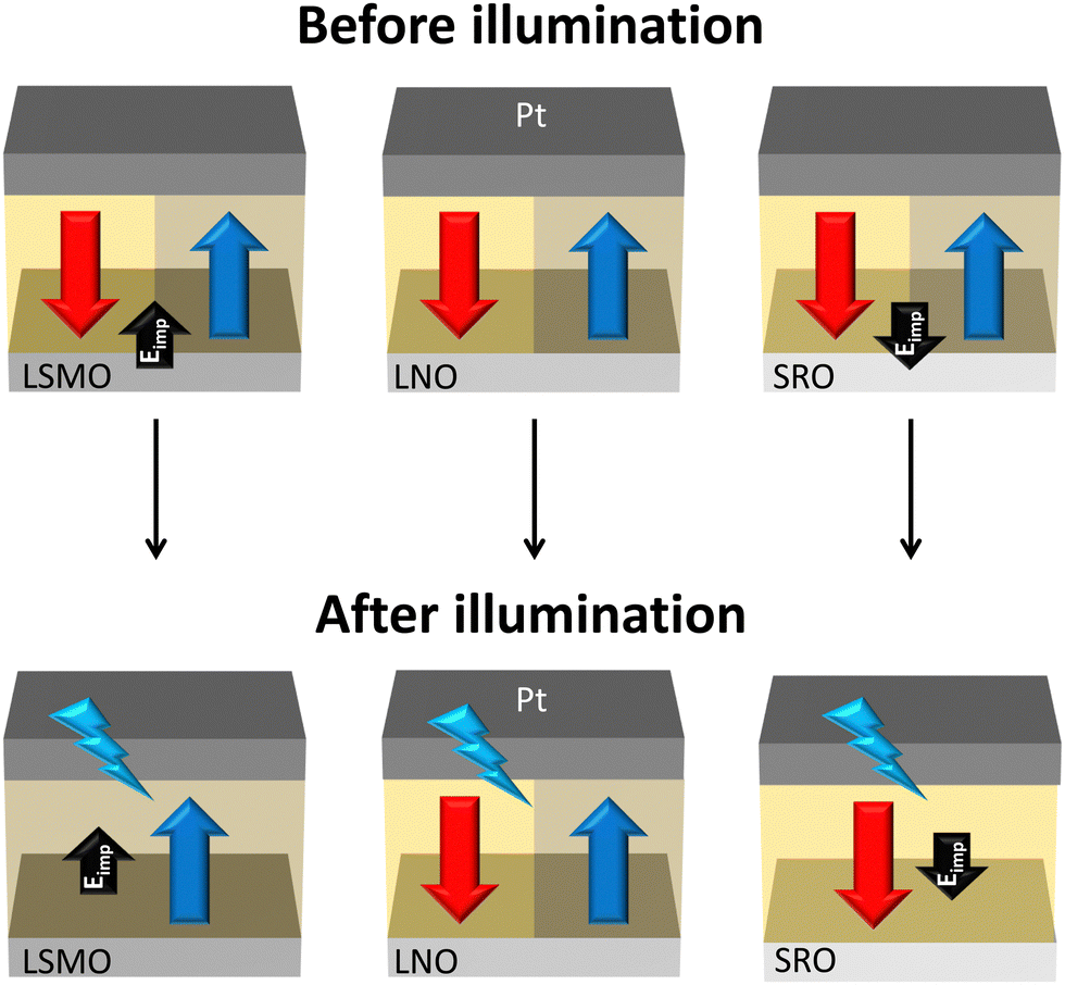 | ||
| Fig. 5 Sketch of the direction of Eimp in the different studied samples. The effect of light on the polarization results in its switching towards the Eimp direction. | ||
To further crosscheck the impact of optically induced switching and the robustness of the effect, top Pt electrodes (see methods) were deposited to build capacitors. PFM data using Pt electrodes are shown in Fig. S11, ESI.†Fig. 6(a) shows I–V characteristics for the BTO/LSMO sample. First of all, it can be appreciated that the I–V characteristics for the pristine state (black line) and that collected after prepoling the sample with a −8 V pulse (500 ms duration) (red line) overlap and display a rectifying behavior suggesting it to be dominated by the presence of a Schottky barrier at the top Pt/BTO and/or bottom BTO/LSMO interfaces. The overlapping of the I–V curves agrees with the fact that the as-grown state is already in the polarization-up state, coinciding with the up state set after applying −8 V. In contrast, after prepoling the sample with a +8 V pulse, which results in polarization pointing downwards, the I–V curve (blue line) clearly indicates a higher conductivity. This implies that the Schottky barrier height has been modified (reduced) when reversing the polarization direction.50 The I–V data is plotted in semilogarithmic scale in Fig. 6(b), where the I–V asymmetry can be better appreciated. It follows that the resistance across the prepared capacitors can be used to inspect the light-induced polarization reversal (the optical transmittance of the 20 nm thick Pt electrode is ≈5%). This is shown in Fig. 6(c) (top panel), where the resistance of the Pt/BTO/LSMO device (computed at V = −1.5 V) is plotted as a function of the V-induced polarization writing and illumination protocol (as indicated in the x-axis). Illumination time dependence experiments show that the resistance change is gradual in a similar manner to the PFM contrast and that it takes around 200 s (Fig. S12, ESI†). Similar data were collected for Pt/BTO/LNO and Pt/BTO/SRO capacitors [Fig. 6(c, central and bottom panels)]. In all cases, the changes of the device resistance either after poling or after illumination are fully consistent with the proposed illumination-triggered polarization reversal mechanism, which indicates that polarization switches towards the as-grown state as dictated by the imprint electric field. Precisely, light induces a resistance change from low to high [from down to up for polarization as indicated in Fig. 6(c)] in the Pt/BTO/LSMO sample and from high to low [up to down as indicated in Fig. 6(c)] for the Pt/BTO/SRO one. No effect of light is observed for the Pt/BTO/LNO sample, and after illumination the resistance state is the same. On the other hand, it is observed that after negative voltage pulse a high resistance state is set and after a positive voltage pulse a low resistance state is set. This holds for all samples: BTO/LSMO, BTO/LNO and BTO/SRO, which we note have a common Pt/BTO interface but different bottom interfaces. This indicates that the Schottky barrier at the top Pt/BTO governs the overall device resistance, which is further modulated by the polarization direction.
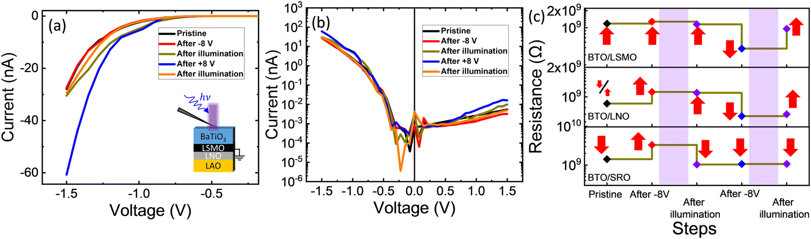 | ||
| Fig. 6 (a) I–V characteristic of the BTO/LSMO sample in the pristine state and after ±8 V prepoling and after ±8 V prepoling and subsequent illumination. (b) The same I–V characteristics with current in semi-log scale. (c) Resistance state measured at −1.5 V for the BTO/LSMO, BTO/LNO and BTO/SRO samples after application of ±8 V prepoling or illumination as indicated. | ||
Conclusions
It has been shown that suitable illumination of ferroelectric BaTiO3 films allows switching of the polarization direction. PFM and SHG data support for optical switching of bulk polarization. More precisely, after suitably pre-poling, the polarization can be optically switched back to its polar as-grown state. It turns out that instrumental to this observation is the presence of an imprint field acting on the ferroelectric layer. We have shown that the selection of the bottom electrode allows to obtain imprint fields in BaTiO3 pointing either upwards/downwards or being negligible, which subsequently determine the polar state of the as-grown BaTiO3 film and ultimately rule the photo-induced polarization switching. It has been also observed that in a metal–ferroelectric–metal configuration using top Pt electrodes, the conductivity is determined by polarization and thus the resistance state can be also controlled by light from high to low and from low to high depending on the ferroelectric imprint direction. The observed selective response provides important insights into the control of ferroelectric polarization by light and might be instrumental for optoelectric memory devices based on ferroelectric materials.Experimental section
Material growth
All oxide films described in the main manuscript were grown by PLD (KrF excimer laser). BTO (65 nm)/LSMO (25 nm)/LNO (30 nm), BTO (65 nm)/LNO (30 nm) and BTO (65 nm)/SRO (30 nm)/LNO (30 nm) were deposited in a single process on LAO (001) single crystal substrates. The LSMO, LNO and SRO layers were grown at 700 °C and 5 Hz of laser frequency, with different oxygen pressure of 0.1 mbar, 0.15 mbar and 0.2 mbar, respectively. The BTO films were grown at a substrate temperature of 700 °C under an oxygen pressure of 0.02 mbar and a laser frequency of 5 Hz. The 60 nm BiFeO3 film on the LSMO buffered SrTiO3 (001) substrate, described in the Supporting Information, was grown by chemical solution deposition.51,52 Top Pt electrodes (20 nm thick, 55 μm in diameter) were deposited by sputtering through a stencil mask.Piezoelectric force microscopy
PFM measurements were performed with an MFP-3D ASYLUM RESEARCH microscope (Oxford Instrument Co.), using the AppNano silicon (n-type) cantilevers with Pt coating (ANSCM-PT-50). To achieve better sensitivity, the dual AC resonance tracking (DART) method was employed.53 PFM voltage hysteresis loops were always performed at remanence using a dwell time of 100 ms. Scanned areas were 20 × 20 μm2 and the electrically written regions were 10 × 10 μm2. Note that the bottom electrode was in all cases grounded and the tip was at bias voltage.Second harmonic generation microscopy
The SHG measurements were performed using a Kerr lens modelocked Ti:sapphire laser (MIRA 900 f, Coherent). This source generates 180 fs pulses at a central wavelength of 810 nm with linear polarization. The laser beam was coupled to an adapted inverted microscope (Eclipse TE2000-U, Nikon). The coupling system included two galvanometric mirrors (Cambridge Technology, UK), a telescope arrangement and a halfwave plate to control the polarization of the excitation beam keep the polarized electric field parallel to the surface of incidence. We used a dichroic mirror (FF670-SDi01, Semrock) to direct the laser to the illumination objective (Nikon 20× NA = 0.75). The optical power on the sample plane was fixed at 25 mW and was maintained at this level in all the experiments. The sample had a tilting angle of 17° with respect to the microscope objective. Note that the used power is much lower to that used to achieve polarization switching by illumination and thus not producing a significant change on the polar state during the measuring time. In addition, the used laser wavelength is long enough to avoid important absorption in the material.Electrical transport
Current–voltage (I–V) measurements were recorded by a Keithley 6517B electrometer, using bipolar triangular excitation signals from +1.5 V to −1.5 V with 500 ms integration time.Conflicts of interest
There are no conflicts to declare.Acknowledgements
Financial support from the Spanish Ministry of Science and Innovation (10.13039/501100011033), through the Severo Ochoa FUNFUTURE (project CEX2019-000917-S funded by MCIN/AEI), project TED2021-130453B-C21 funded by MCIN/AEI and European Union NextGenerationEU/PRTR, and projects PID2020-112548RB-I00 and PID2019-107727RB-I00 funded by MCIN/AEI, and project LINKA20338 from CSIC through the i-LINK program are acknowledged. Project supported by a 2020 Leonardo Grant for Researchers and Cultural Creators, BBVA Foundation. H.T. is financially supported by China Scholarship Council (CSC), grant No. 201906050014. H.T.'s work has been done as a part of his PhD. program in Materials Science at Universitat Autònoma de Barcelona. G. C-O and P.L-A acknowledge funding from CEX2019-000910-S [MICINN/AEI/10.13039/501100011033], Fundació Cellex, Fundació Mir-Puig, Generalitat de Catalunya through “CERCA” and Laserlab-Europe (871124). We acknowledge support of the publication fee by the CSIC Open Access Publication Support Initiative through its Unit of Information Resources for Research (URICI). Pamela Machado and Mariona Coll are acknowledged for providing BiFeO3 films.References
- C. Sun, M. T. Wade, Y. Lee, J. S. Orcutt, L. Alloatti, M. S. Georgas, A. S. Waterman, J. M. Shainline, R. R. Avizienis and S. Lin, Nature, 2015, 528, 534–538 CrossRef CAS PubMed.
- G. Indiveri and R. Douglas, Science, 2000, 288, 1189–1190 CrossRef PubMed.
- T. Choi, S. Lee, Y. Choi, V. Kiryukhin and S.-W. Cheong, Science, 2009, 324, 63–66 CrossRef CAS PubMed.
- R. Guo, L. You, Y. Zhou, Z. S. Lim, X. Zou, L. Chen, R. Ramesh and J. Wang, Nat. Commun., 2013, 4, 1990 CrossRef PubMed.
- F. M. Liu, I. Fina, D. Gutierrez, G. Radaelli, R. Bertacco and J. Fontcuberta, Adv. Electron. Mater., 2015, 1, 1500171 CrossRef.
- V. Garcia, S. Fusil, K. Bouzehouane, S. Enouz-Vedrenne, N. D. Mathur, A. Barthelemy and M. Bibes, Nature, 2009, 460, 81–84 CrossRef CAS PubMed.
- S. Mathews, R. Ramesh, T. Venkatesan and J. Benedetto, Science, 1997, 276, 238–240 CrossRef CAS PubMed.
- G. Di Martino and S. Tappertzhofen, Nanophotonics, 2019, 8, 1579–1589 Search PubMed.
- B. Kundys, Applied Physics Reviews, 2015, 2, 011301 CrossRef.
- F. Rubio-Marcos, D. A. Ochoa, A. Del Campo, M. A. García, G. R. Castro, J. F. Fernández and J. E. García, Nat. Photonics, 2018, 12, 29–32 CrossRef CAS.
- G. Vats, Y. Bai, D. Zhang, J. Juuti and J. Seidel, Adv. Opt. Mater., 2019, 7, 1800858 CrossRef.
- Y.-D. Liou, Y.-Y. Chiu, R. T. Hart, C.-Y. Kuo, Y.-L. Huang, Y.-C. Wu, R. V. Chopdekar, H.-J. Liu, A. Tanaka and C.-T. Chen, Nat. Mater., 2019, 18, 580–587 CrossRef CAS PubMed.
- J. Guo, W. Chen, H. Chen, Y. Zhao, F. Dong, W. Liu and Y. Zhang, Adv. Opt. Mater., 2021, 9, 2002146 CrossRef CAS.
- W. Q. Liao, B. B. Deng, Z. X. Wang, T. T. Cheng, Y. T. Hu, S. P. Cheng and R. G. Xiong, Adv. Science, 2021, 8, 2102614 CrossRef CAS PubMed.
- P. Wurfel and I. Batra, Phys. Rev. B, 1973, 8, 5126 CrossRef CAS.
- Z.-D. Luo, X. Xia, M.-M. Yang, N. R. Wilson, A. Gruverman and M. Alexe, ACS Nano, 2019, 14, 746–754 CrossRef PubMed.
- A. Lipatov, P. Sharma, A. Gruverman and A. Sinitskii, ACS Nano, 2015, 9, 8089–8098 CrossRef CAS PubMed.
- T. Li, A. Lipatov, H. Lu, H. Lee, J.-W. Lee, E. Torun, L. Wirtz, C.-B. Eom, J. Íñiguez and A. Sinitskii, Nat. Commun., 2018, 9, 3344 CrossRef PubMed.
- A. Lipatov, N. S. Vorobeva, T. Li, A. Gruverman and A. Sinitskii, Adv. Electron. Mater., 2021, 7, 2001223 CrossRef CAS.
- J. Wang, G. Liu, D. Sando, V. Nagarajan and J. Seidel, Appl. Phys. Lett., 2017, 111, 092902 CrossRef.
- W. Song, P. A. Salvador and G. S. Rohrer, ACS Appl. Mater. Interf., 2018, 10, 41450–41457 CrossRef CAS PubMed.
- H. Lee, T. H. Kim, J. J. Patzner, H. Lu, J.-W. Lee, H. Zhou, W. Chang, M. K. Mahanthappa, E. Y. Tsymbal and A. Gruverman, Nano Lett., 2016, 16, 2400–2406 CrossRef CAS PubMed.
- C. Blaser and P. Paruch, New J. Phys., 2015, 17, 013002 CrossRef CAS.
- A. V. Ievlev, A. N. Morozovska, V. Y. Shur and S. V. Kalinin, Appl. Phys. Lett., 2014, 104, 092908 CrossRef.
- I. Spasojević, G. Sautier, J. Caicedo, A. Verdaguer and N. Domingo, Appl. Surf. Sci., 2021, 565, 150288 CrossRef.
- M. M. Yang and M. Alexe, Adv. Mater., 2018, 30, 1704908 CrossRef PubMed.
- Z.-D. Luo, D.-S. Park, M.-M. Yang and M. Alexe, ACS Appl. Mater. Interf., 2019, 11, 8276–8283 CrossRef CAS PubMed.
- N. Dix, I. Fina, R. Bachelet, L. Fabrega, C. Kanamadi, J. Fontcuberta and F. Sanchez, Appl. Phys. Lett., 2013, 102, 172907 CrossRef.
- M. Scigaj, N. Dix, I. Fina, R. Bachelet, B. Warot-Fonrose, J. Fontcuberta and F. Sanchez, Appl. Phys. Lett., 2013, 102, 112905 CrossRef.
- J. Lyu, I. Fina, R. Solanas, J. Fontcuberta and F. Sanchez, Sci. Rep., 2018, 8, 495 CrossRef PubMed.
- B. C. Jeon, D. Lee, M. H. Lee, S. M. Yang, S. C. Chae, T. K. Song, S. D. Bu, J.-S. Chung, J.-G. Yoon and T. W. Noh, Adv. Mater., 2013, 25, 5643–5649 CrossRef CAS PubMed.
- V. P. Afanasjev, A. A. Petrov, I. P. Pronin, E. A. Tarakanov, E. J. Kaptelov and J. Graul, J. Phys.: Condens. Matter, 2001, 13, 8755–8763 CrossRef CAS.
- P. Maksymovych, N. Balke, S. Jesse, M. Huijben, R. Ramesh, A. P. Baddorf and S. V. Kalinin, Journal of Materials Science, 2009, 44, 5095–5101 CrossRef CAS.
- D. Lee, B. C. Jeon, A. Yoon, Y. J. Shin, M. H. Lee, T. K. Song, S. D. Bu, M. Kim, J. S. Chung and J. G. Yoon, Adv. Mater., 2014, 26, 5005–5011 CrossRef CAS PubMed.
- P. Yu, W. Luo, D. Yi, J. Zhang, M. Rossell, C.-H. Yang, L. You, G. Singh-Bhalla, S. Yang and Q. He, Proc. Natl. Acad. Sci. U. S. A., 2012, 109, 9710–9715 CrossRef CAS PubMed.
- Y. Q. Zhan, I. Bergenti, L. E. Hueso, V. Dediu, M. P. de Jong and Z. S. Li, Phys. Rev. B: Condens. Matter Mater. Phys., 2007, 76, 045406 CrossRef.
- H. Wang, Y. Bai, X. Ning and Z. Wang, RSC Advances, 2015, 5, 104203–104209 RSC.
- M. Minohara, I. Ohkubo, H. Kumigashira and M. Oshima, Appl. Phys. Lett., 2007, 90, 132123 CrossRef.
- H. P. Bonzel and T. E. Fischer, Surf. Sci., 1975, 51, 213–227 CrossRef CAS.
- C. Weymann, C. Lichtensteiger, S. Fernandez-Peña, A. B. Naden, L. R. Dedon, L. W. Martin, J.-M. Triscone and P. Paruch, Adv. Electron. Mater., 2020, 6, 2000852 CrossRef CAS.
- S. Wemple, Phys. Rev. B, 1970, 2, 2679 CrossRef.
- M. Choi, F. Oba and I. Tanaka, Appl. Phys. Lett., 2011, 98, 172901 CrossRef.
- M. L. Moreira, M. F. C. Gurgel, G. P. Mambrini, E. R. Leite, P. S. Pizani, J. A. Varela and E. Longo, J. Phys. Chem. A, 2008, 112, 8938–8942 CrossRef CAS PubMed.
- X. Long, H. Tan, F. Sánchez, I. Fina and J. Fontcuberta, Nat. Commun., 2021, 12, 382 CrossRef CAS PubMed.
- M. Saeed, W. Uddin, S. Ali, A. S. Saleemi, K. Khan, S. U. Rehman and M. Khan, Phys. B, 2021, 614, 412962 CrossRef CAS.
- H.-S. Lee and H.-H. Park, Adv. Condens. Matter Phys., 2015, 2015, 746475 Search PubMed.
- V. M. Fridkin, Photoferroelectrics, Springer-Verlag, Berlin Heidelberg, New York, 1979 Search PubMed.
- J. Wang, B. Vilquin and N. Barrett, Appl. Phys. Lett., 2012, 101, 092902 CrossRef.
- J. Nordlander, G. De Luca, N. Strkalj, M. Fiebig and M. Trassin, Applied Sciences, 2018, 8, 570 CrossRef.
- L. Pintilie and M. Alexe, J. Appl. Phys., 2005, 98, 124103 CrossRef.
- P. Machado, I. Cano, C. Menéndez, C. Cazorla, H. Tan, I. Fina, M. Campoy-Quiles, C. Escudero, M. Tallarida and M. Coll, J. Mater. Chem. C, 2021, 9, 330–339 RSC.
- P. Machado, M. Scigaj, J. Gazquez, E. Rueda, A. Sanchez-Diaz, I. Fina, M. Gibert-Roca, T. Puig, X. Obradors, M. Campoy-Quiles and M. Coll, Chem. Mater., 2019, 31, 947–954 CrossRef CAS PubMed.
- B. J. Rodriguez, C. Callahan, S. V. Kalinin and R. Proksch, Nanotechnology, 2007, 18, 475504 CrossRef.
Footnote |
| † Electronic supplementary information (ESI) available: Complementary experiments and summary of the lattice parameters of the characterized samples. See DOI: https://doi.org/10.1039/d2mh00644h |
| This journal is © The Royal Society of Chemistry 2022 |