
 Open Access Article
 This Open Access Article is licensed under a
 Creative Commons Attribution 3.0 Unported Licence
Two-photon absorption in halide perovskites and their applications
Junsheng
Chen†
 a,
Wei
Zhang†
b and
Tönu
Pullerits
*b
a,
Wei
Zhang†
b and
Tönu
Pullerits
*b
aNano-Science Center & Department of Chemistry, University of Copenhagen, Universitetsparken 5, 2100 Copenhagen, Denmark
bChemical Physics and NanoLund, Lund University, Box 124, Lund 22100, Sweden. E-mail: tonu.pullerits@chemphys.lu.se
First published on 27th May 2022
Abstract
Active research on halide perovskites has given us a deep understanding of this family of materials and their potential for applications in advanced optoelectronic devices. One of the prominent outcomes is the use of perovskite materials for nonlinear optical applications. Two-photon absorption in perovskites, in particular their nanostructures, has been extensively studied and shows huge promise for many applications. However, we are still far from a thorough understanding of two-photon absorption in halide perovskites from a micro to macro perspective. Here we summarize different techniques for studying the two-photon absorption in nonlinear optical materials. We discuss the in-depth photophysics in two-photon absorption in halide perovskites. A comprehensive summary about the factors which influence two-photon absorption provides the direction to improve the two-photon absorption properties of halide perovskites. A summary of the recent applications of two-photon absorption in halide perovskites provides inspirations for engineers to utilize halide perovskites in two-photon absorption device development. This review will help readers to have a comprehensive and in-depth understanding of the research field of two-photon absorption of halide perovskites from microscopic mechanisms to applications. The article can serve as a manual and give inspiration for future researchers.
 Junsheng Chen | Junsheng Chen received his double BS degrees in materials physics and management at China University of Petroleum (east) in 2010. He received his PhD degree in 2018 at Lund University (supervisor: Prof. Tönu Pullerits). Then he carried out postdoctoral work at the University of Copenhagen (UCPH). In 2019–2020, he worked on developing control components for semiconductor devices at Bombardier. He is currently an assistant professor at UCPH. His work explores functions and underlying photophysical processes of fluorescent nanomaterials by time-resolved optical spectroscopies. |
 Wei Zhang | Wei Zhang obtained his PhD degree in Physical Chemistry from the Institute of Chemistry, Chinese Academy of Sciences (ICCAS) in 2020 under the supervision of Prof. Andong Xia. Then he worked as a postdoc fellow in Prof. Tönu Pullerits’ group at Lund University, Sweden. Now he is a research associate professor in the University of Science and Technology of China (USTC). His research focus on photophysics of organics and inorganics using the time-resolved spectroscopy. |
 Tönu Pullerits | Tönu Pullerits obtained his PhD from the Institute of Physics at Tartu University, Estonia, in 1991. He pursued his postdoc work in Free University of Amsterdam (1992–1993), Umeå University (1993–1994). He moved to Lund University in 1994 where he is currently a full professor and the head of the Division of Chemical Physics. He is a member of the Royal Swedish Academy of Sciences since 2016. His research interests include energy transport in molecular systems, ultrafast charge carrier dynamics and photophysics in photovoltaic materials, and coherent multidimensional spectroscopy. |
1. Introduction
In semiconductor materials, two-photon absorption (TPA) is a process where an electron is excited from the valence band to the conduction band by simultaneously absorbing two photons without populating any real intermediate state (Fig. 1). Since the transition conserves energy, the individual photon energies can be lower than the bandgap of the material. The initial excitation have significant energy above the band edge and will rapidly relax towards the lowest excited states where the charge carriers can recombine radiatively and emit a photon with energy higher than the excitation photons. Because of its high nonlinearity, the TPA process shows a higher spatial confinement to the focal point of the excitation beam compared to one-photon absorption (OPA). Also, the used low-energy photons exhibit a typical longer penetration depth and lower biological damage compared to the higher energy photons which are used in the OPA process. Consequently, TPA materials show attractive applications.1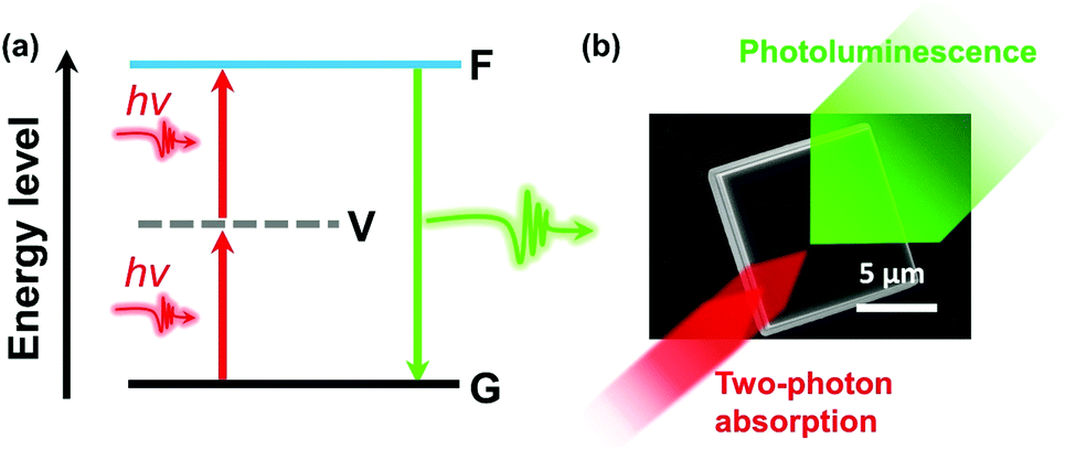 | ||
| Fig. 1 (a) Schematic diagram of TPA. G, ground state; V, virtual state; F, final excited state. (b) Illustration of TPA and photoluminescence in a halide perovskite microcrystal. | ||
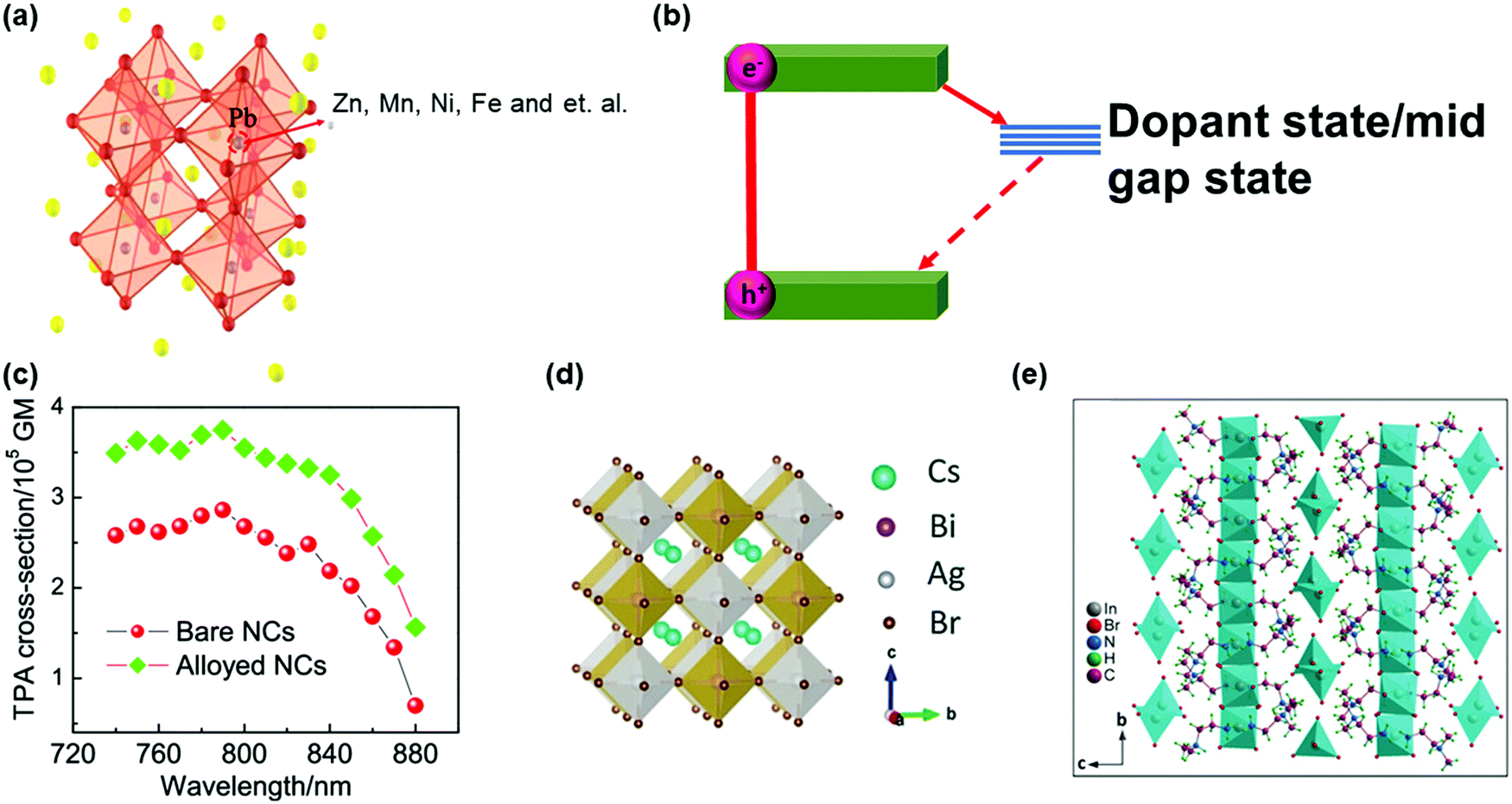
Perovskite was first referred to as the mineral CaTiO3, which was discovered by Gustav Rose in the Ural Mountains in 1839. Since then, perovskite has been used to refer to the class of compounds which share a similar crystal structure to CaTiO3. In the past decade, lead halide perovskites with the general formula APbX3 (X = Cl, Br and I), where A is a cation such as cesium (Cs), methylammonium (MA), or formamidinium (FA), showed high performance as active materials for solar cells owing to their superior optical and electronic properties, such as strong broadband absorption, defect tolerance, efficient charge carrier generation and transportation. In a typical cubic structure of lead halide perovskites (Fig. 2a), one divalent lead cation (Pb2+) with a 6-fold coordination forms an octahedron unit together with 6 halide anions ([PbX6]4−). The monovalent cation A+ is in the middle of the cube and is surrounded by eight octahedra. The angle between the octahedra can be changed using different factors. For example, with a decrease in temperature, the octahedra tilt and, as a result, the lead halide perovskites undergo phase transitions including tetragonal, orthorhombic, monoclinic, and rhombohedral phases. It has been reported that lead halide perovskites with different phases show different optical and electronic properties, due to the direct relation between the electronic structures and the phase structures.2 The structure can be changed directly via chemical composition as well. For example, if the cation A+ is replaced by large organic molecular cations, the three-dimensional perovskite structure will be broken down since the anion will be too large to properly fit into the structure. Such loss of the crystal stability is quantified via the violation of the Goldschmidt tolerance factor.3 As a result, the dimensionality can be reduced from three-dimensional down to zero-dimensional PbX6 octahedral clusters.4–6 Note that the dimensionality discussed here refers to the connectivity of the corner-sharing ([PbX6]4−) octahedra in the crystal structure not the physical form of the materials. For example, in the two-dimensional structure (Fig. 2b),7 one or several layers of lead–halide octahedra are surrounded by large organic cations. This type of perovskite structure belongs to the Ruddlesden–Popper8 or Dion–Jacobson phase.9 The lead cation can be replaced by other metal cations (such as Sn, Ge, Bi and Sb) and form lead-free halide perovskites. New crystal structures and new optoelectronic properties are introduced into these lead-free halide perovskites.10,11 For example, when a lead cation is replaced by a heterovalent element (e.g. Bi3+ in Fig. 2c), a vacancy-ordered perovskite structure is formed, which can be viewed as a tripling of the traditional perovskite unit cell with only two-thirds of the octahedral positions fully occupied.12 Furthermore, the lead cation can be doped with other elements, such as Mn2+, Zn2+ and Ca2+. Owing to the ionic nature of lead halide perovskites, the halide ions (X) can be exchanged between Cl−, Br− and I−, and as a result the bandgap of lead halide perovskites can be tuned in a wide range (Fig. 2d).13 The wide variety of chemical composition offers different ways to tune the optical and electronic properties of halide perovskites via chemical doping/substitution. Their optical and electronic properties can also be further tuned by their morphologies, such as size and shape. By effectively managing the thermodynamics and kinetics of nucleation and growth, halide perovskites with different morphologies have been reported, such as polycrystalline thin films, millimeter- or centimeter-sized single crystals, microcrystals, single-crystal thin films, micro-/nano-plates or rods, and nanocrystals.14
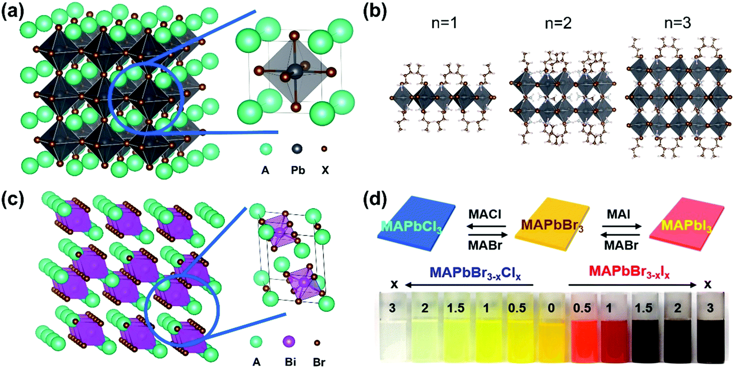 | ||
| Fig. 2 (a) Crystal structure of 3D lead halide perovskite (A: cations, X = Cl, Br, I). (b) Crystal structures of 2D lead iodide perovskites with butylammonium (BA+) as a spacer organic cation BA2(CH3NH3)n−1PbnI3n+1 (n = 1–3). (c) Crystal structure of a vacancy-ordered perovskite Cs3Bi2Br9. (d) Photograph of MAPbBr3−xClx and MAPbBr3−xIx colloidal nanocrystal solutions, where x = 0, 0.5, 1, 1.5, 2, and 3. (d) Reprinted with permission from ref. 13. Copyright 2015 American Chemical Society. | ||
The optical and electronic properties of halide perovskites can be tuned using the above-mentioned factors such as chemical composition, structure, and morphology. Several review articles have discussed how to tune their linear optical properties using these factors.2,14–16 Beside their superior properties in the linear optical response regime, halide perovskites also show good nonlinear optical properties, especially in the TPA process.6,17–24 Their tunable bandgap, high photoluminescence quantum yield and low-cost fabrication support their applications in both linear and nonlinear optical response regimes. In particular, the TPA process has been applied in different applications, such as up-conversion laser, sub-bandgap photodetection, bioimaging,25 two-photon excited photoluminescence/photocurrent mapping, and optical limiting (Fig. 3).26,27
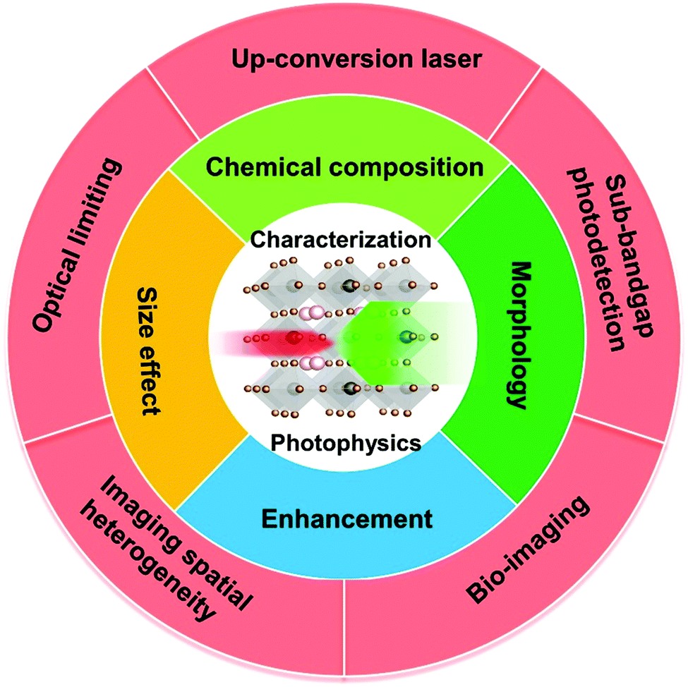 | ||
| Fig. 3 Schematic diagram of factors influencing nonlinear optical characteristics and applications of halide perovskites. | ||
Here we review the recent studies on how the chemical composition, structure and morphology influence the TPA in halide perovskites. We summarize the techniques for measuring the TPA processes in halide perovskites. Then, we highlight the photophysics in two-photon excited halide perovskites. We discuss how different factors influence the TPA process and how we can utilize the TPA process in halide perovskites for advanced optoelectronic applications. Finally, we discuss the main challenges and opportunities for future research in this area. In this review, we aim to provide the readers a clear picture about the TPA process in halide perovskites. The review also supplies design strategies for developing advanced TPA materials for optoelectronic applications.
2. Two-photon absorption
TPA is a process where a material simultaneously absorbs two photons. The total energy of the two photons is equal to the excited state.28–30 This phenomenon was first predicted theoretically in 1931 by Maria Goeppert Mayer.31 With the development of laser technology, TPA was first observed experimentally by Kaiser and Garrett in 1961.32 Since then, the TPA phenomenon has been extensively investigated in a large variety of materials.19,28,30,33,34From the quantum mechanics perspective, the transition that is induced by the absorption of two photons is often explained as involving a virtual state (Fig. 1).35,36 This can be thought as the initial interaction between one photon and the material that results in a temporary state with an energy level of hν. The virtual state is not an eigenstate of the material and rather serves as a visualization tool. The expression for the TPA probability derived via perturbation theory in terms of sum over states allows an intuitive picture of the process where all excited states act as the possible virtual intermediates via the tails of their absorption. Since the energy difference between the photon and the corresponding states is large, the quantum mechanical amplitude (not population) of the intermediate is nonzero only for an ultra-short time interval τV (∼10−15–10−16 s). If another photon interacts with the system during τV, the final exited state can be populated.29,35,37 The “simultaneously” herein means that there are two photons interacting with the system within τV and no intermediate state is really populated.29
From the coupled wave perspective the electric field E of the light interacts with electrons in the dielectric material inducing polarization P as38,39
| P = ε0(χ(1)E1 + χ(2)E2 + χ(3)E3 + …), | (1) |
 | (2) |
 | (3) |
 | (4) |
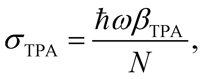
σ TPA is widely used to describe the TPA probability of single molecules or nanomaterials. βTPA is the characteristic parameter for describing the TPA probability of bulk materials, such as films and mm–cm size single crystals. To compare the TPA probability of bulk materials and single nanomaterials, one needs to normalize the size of the nanomaterials. The details are described in Table 1.
| Perovskites | TPA cross-section (10−50 cm4 s photon−1) | TPA coefficient (cm GW−1) | E g (eV) | Excitation wavelength (nm) | Technique (pulse duration, repetition rate) | Morphology | Dimensionality | Size (nm) | Ref. |
|---|---|---|---|---|---|---|---|---|---|
a The TPA coefficient is calculated based on the TPA cross-section, and the size of the nanomaterials is normalized. 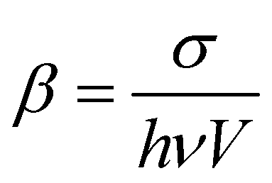 , in which σ is the TPA cross-section of the nanomaterials, h is the Planck constant, ν is the excitation photon frequency, and V is the volume of the nanomaterials.
b The value is measured in nanocrystal solution; it represents the TPA coefficient of the solution with a given nanocrystal concentration. It is not an intrinsic property of the nanocrystals.
c The value is optical bandgap, derived based on the photoluminescence peak position.
d The average value is used for the TPA coefficient calculation.
e The excitation photon energy is very close to the bandgap energy. This might be an OPA process. , in which σ is the TPA cross-section of the nanomaterials, h is the Planck constant, ν is the excitation photon frequency, and V is the volume of the nanomaterials.
b The value is measured in nanocrystal solution; it represents the TPA coefficient of the solution with a given nanocrystal concentration. It is not an intrinsic property of the nanocrystals.
c The value is optical bandgap, derived based on the photoluminescence peak position.
d The average value is used for the TPA coefficient calculation.
e The excitation photon energy is very close to the bandgap energy. This might be an OPA process.
|
|||||||||
| CsPbCl3 | 3.8 × 10⁴ | 10.7a | 3.02 | 700 | Z-scan (100 fs, 80 MHz) | Quantum dots | 3D | 5 | 106 |
| — | 8.0 × 10⁻³ | 2.93 | 800 | Z-scan (50 fs, 1 kHz) | Microplates | 3D | — | 203 | |
| — | 3.8 | 3.00c | 800 | Z-scan (50 fs, 1 kHz) | Microcrystal | 3D | — | 99 | |
| — | 1.36 × 10⁻²![[thin space (1/6-em)]](https://www.rsc.org/images/entities/char_2009.gif) b b |
2.78 | 787 | Z-scan (396 fs, 1 kHz) | Nanocrystals | 3D | — | 204 | |
| 2.0 × 10⁴ | — | 3.03 | 700–925 | Z-scan (— fs, 1 kHz) | Nanocrystals | 3D | 22 | 107 | |
| 7.0 × 10³ | 0.23 | — | 620 | Z-scan (100 fs, 1 kHz) | Nanocrystals | 3D | 9.8 | 109 | |
| CsPb(Cl0.53Br0.47) | 2.8 × 10⁴ | 0.58 | — | 620 | Z-scan (100 fs, 1 kHz) | Nanocrystals | 3D | 11.6 | 109 |
| CsPbCl1.5Br1.5 | 8.8 × 10⁴ | 16.4a | 2.61 | 800 | Z-scan (100 fs, 80 MHz) | Quantum dots | 3D | 5–7d | 106 |
| 2.7 × 10⁵ | — | 2.77 | 700–925 | Z-scan (— fs, 1 kHz) | Nanocrystals | 3D | 16 | 107 | |
| CsPbClBr2 | 1.6 × 10⁵ | 3.7a | 2.46 | 800 | Z-scan (— fs, 1 kHz) | Quantum dots | 3D | 12 | 65 |
| CsPbCl2Br | 1.1 × 10⁵ | 2.6a | 2.76 | 800 | Z-scan (— fs, 1 kHz) | Quantum dots | 3D | 12 | 65 |
| CsPb(Cl0.2Br0.8)3 | 1.2 × 10⁶ | 7.5a | 2.51 | 800 | Z-scan (100 fs, 1 kHz) | Nanorods | 3D | Length: 64 | 132 |
| Diameter: 11.3 | |||||||||
| CsPbBr3 | 1.8 × 10⁵ | 33.6a | 2.30 | 800 | Z-scan (100 fs, 80 M Hz) | Quantum dots | 3D | 6 | 106 |
| — | 10 | 2.25 | 960 | Z-scan (30 ps, 50 Hz) | Single crystals | 3D | — | 79 | |
| — | 2.9 | 2.27 | 800 | Nonlinear transmission measurement (90 fs, 1 kHz) | Single crystals | 3D | — | 100 | |
| — | 19.4 | 2.32c | 800 | Z-scan (35 fs, 1 kHz) | Film | 3D | — | 146 | |
| — | 10.5 | 2.26 | 800 | Nonlinear transmission measurement (100 fs, 1 kHz) | Micocrystal | 3D | — | 89 | |
| — | 3.2 × 10⁻²b |
2.39 | 787 | Z-scan (396 fs, 1 kHz) | Nanocrystals | 3D | — | 204 | |
| 1.2 × 10⁵ | 6.6a | 2.42 | 800 | Z-scan (100 fs, 1 kHz) | Nanocrystals | 3D | 9 | 63 | |
| — | (4.7–10.9) | 2.36 | 800 | Z-scan (80 fs, 1 kHz) | Nanosheets | 3D | 104.6–195.4 | 80 | |
| — | 2.8 × 10³ | 2.42 | 720 | Z-scan (100 fs, 1 kHz) | Quantum dots coated with zeolite | 3D | 10 | 149 | |
| — | 3.0 × 10³ | 2.42 | 720 | Z-scan (100 fs, 1 kHz) | Quantum dots coated with zeolite | 3D | 10 | 149 | |
| — | 8.5 × 10⁻² | 2.42 | 800 | Z-scan (100 fs, 1 kHz) | Quantum dots | 3D | 11.4 | 205 | |
| (1.8–23.6) × 106 | (1.1–11) × 102a |
2.40 | 675–1000 | Z-scan (50 fs, 1 kHz) | Nanocrystals | 3D | 9 | 83 | |
| 2.0 × 10⁶ | 1.1 × 10²a |
2.40 | 800 | Z-scan (50 fs, 1 kHz) | Nanocrystals | 3D | 9 | 83 | |
| 2.2 × 10⁵ | 4.7a | 2.40 | 800 | Z-scan (— fs, 1 kHz) | Quantum dots | 3D | 12.4 | 65 | |
| 2.7 × 10⁶ | 1.5 × 10²a |
2.40 | 800 | Z-scan (90 fs, 1 k Hz) | Nanocrystals | 3D | 9 | 67 | |
| 1.4 × 10⁵ | — | 2.41 | 750–925 | Z-scan (— fs, 1 kHz) | Nanocrystals | 3D | 20 | 107 | |
| 1.82 × 10⁵ | 50.3a | 2.74 | 800 | Z-scan (100 fs, 1 kHz) | Nanoplate | 3D | 10.4 × 7.8 × 1.8 | 129 | |
| 1.05 × 10⁵ | 10.9a | 2.57 | 800 | Z-scan (100 fs, 1 kHz) | Nanocrystals | 3D | 7.3 | 129 | |
| 3.68 × 10⁴ | 0.19a | 2.39 | 800 | 2PPL (100 fs, 1 kHz) | Nanocrystals | 3D | 20 | 130 | |
| 1.8 × 10⁵ | 8.7a | — | 800 | Transient absorption measurement (120 fs, 1 kHz) | Nanocrystals | 3D | 9 | 77 | |
| 9.8 × 10⁵ | 22.9a | — | 800 | Z-scan (70 fs, 1 kHz) | Nanocrystals | 3D | 12 | 131 | |
| 1.5 × 10⁶ | 9.3a | 2.42 | 800 | Z-scan (100 fs, 1 kHz) | Nanorods | 3D | Length: 61.3 | 132 | |
| Diameter: 11.6 | |||||||||
| 8.5 × 10⁴ | 0.2a | — | 800 | Z-scan (100 fs, 80 MHz) | Nanocrystals | 3D | 25 | 25 | |
| 4.9 × 10⁵ | 12.3a | — | 800 | Z-scan (100 fs, 80 MHz) | Nanoplatelets | 3D | Length: 20 | 25 | |
| Thickness: 4 | |||||||||
| 2.1 × 10⁵ | 0.5a | — | 800 | Z-scan (100 fs, 80 MHz) | Nanorod | 3D | Length: 200 | 25 | |
| Thickness: 10 | |||||||||
| PEG coated CsPbBr3 | 8.1 × 10⁴ | — | — | 800 | Z-scan (100 fs, 80 MHz) | Nanocrystals | 3D | 35 | 25 |
| PEG coated CsPbBr3 | 4.8 × 10⁵ | — | — | 800 | Z-scan (100 fs, 80 MHz) | Nanoplatelets | 3D | Length: 20 | 25 |
| Thickness: 4 | |||||||||
| PEG coated CsPbBr3 | 2.3 × 10⁵ | — | — | 800 | Z-scan (100 fs, 80 MHz) | Nanorod | 3D | Length: 200 | 25 |
| Thickness: 10 | |||||||||
| Cs4PbBr6 | 2.3 × 10⁷ | 1.2 × 10²a |
4.00 | 800 | Z-scan (70 fs, 1 kHz) | Nanocrystals | 0D | 20 | 206 |
| 4.8 × 10⁶ | 1.7 × 10²a |
4.00 | 800 | Z-scan (70 fs, 1 kHz) | Nanocrystals | 0D | 10.5 | 206 | |
| CsPb(Br0.85I0.15)3 | 2.4 × 10⁶ | 13.9a | 2.36 | 800 | Z-scan (100 fs, 1 kHz) | Nanorods | 3D | Length: 62.8 | 132 |
| Diameter: 11.9 | |||||||||
| CsPbBr1.5I1.5 | 3.2 × 10⁵ | — | 2.11 | 700–1500 | Z-scan (100 fs, 80 M Hz) | Quantum dots | 3D | — | 106 |
| 1.4 × 10⁴ | — | 2.10 | 750–925 | Z-scan (— fs, 1 kHz) | Nanocrystals | 3D | 20 | 107 | |
| 2.7 × 10⁶ | 42.1a | 2.16 | 1030 | Z-scan (340 fs, 1 kHz) | Quantum dots | 3D | 15 | 82 | |
| CsPbBr0.5I2.5 | 6.7 × 10⁵ | 1.94 | 700–1500 | Z-scan (100 fs, 80 M Hz) | Quantum dots | 3D | — | 106 | |
| CsPbBrI2 | 2.6 × 10⁵ | 6.1a | 2.11 | 800 | Z-scan (— fs, 1 kHz) | Quantum dots | 3D | 12 | 65 |
| CsPbBr2.7I0.3 | (0.3–3) × 105 | — | 2.64 | 720–880 | Nonlinear transmittance (100 fs, — kHz) | Nanoplatelets | 3D | Length: 17.2 | 207 |
| Width: 8.7 | |||||||||
| Thickness: 2.4 | |||||||||
| 3 × 10⁵ | 33.7a | 2.64 | 800 | Nonlinear transmittance (100 fs, —kHz) | Nanoplatelets | 3D | Length: 17.2 | 207 | |
| Width: 8.7 | |||||||||
| Thickness: 2.4 | |||||||||
| (0.4–4.1) × 106 | No need to calculate | 2.35 | 720–880 | Nonlinear transmittance (100 fs, — kHz) | Nanoplatelets | 3D | Length: 23.5 | 207 | |
| Width: 14.8 | |||||||||
| Thickness: 3.6 | |||||||||
| 4 × 10⁶ | 1.3 × 10²a |
2.35 | 800 | Nonlinear transmittance (100 fs, — kHz) | Nanoplatelets | 3D | Length: 23.5 | 207 | |
| Width: 14.8 | |||||||||
| Thickness: 3.6 | |||||||||
| 1.6 × 10⁶ | 9.4a | 2.64 | 800 | Z-scan (100 fs, 1 kHz) | Nanocrystals | 3D | 19 | 135 | |
| 7.5 × 10⁵ | 30.3a | 2.26 | 800 | Z-scan (100 fs, 1 kHz) | Nanoplates | 3D | 16 | 135 | |
| 26 | |||||||||
| 2.4 | |||||||||
| CsPbI3 | 2.1 × 10⁶ | — | 1.73 | 700–1500 | Z-scan (100 fs, 80 MHz) | Quantum dots | 3D | 7 | 106 |
| 2.1 × 10⁴ | — | 1.80 | 750–925 | Z-scan (— fs, 1 kHz) | Nanocrystals | 3D | 16 | 107 | |
| 6.8 × 10⁶ | 1.1 × 10²a |
1.85 | 800 | 2PPL measurement (4 ps, 2 MHz) | Nanocrystals | 3D | 13.5 | 75 | |
| (0.5–2.8) × 105 | 1.80 | 740–880 | Z-scan (100 fs, 1 kHz) | Nanocrystals | 3D | 12.7 | 121 | ||
| 2.6 × 10⁵ | 5.1a | 1.80 | 800 | Z-scan (100 fs, 1 kHz) | Nanocrystals | 3D | 12.7 | 121 | |
| 1.2 × 10⁶ | 14.3a | 1.80 | 800 | Z-scan (100 fs, 1 k Hz) | Nanocrystals | 3D | 15 | 135 | |
| CsPb0.8Zn0.2I3 | (1.5–3.8) × 105 | 1.81 | 740–880 | Z-scan (100 fs, 1 kHz) | Nanocrystals | 3D | 12.5 | 121 | |
| 3.6 × 10⁵ | 7.4a | 1.81 | 800 | Z-scan (100 fs, 1 kHz) | Nanocrystals | 3D | 12.5 | 121 | |
| CsPbCl3:Mn | 8.7 × 10⁴ | 5.7a | 3.22 | 620 | Z-scan (— fs, 1 kHz) | Nanocrystals | 3D | 7.8 nm | 120 |
| CsPbCl3:Mn | 3.8 × 10⁵ | 40.8a | 3.25 | 620 | Z-scan (— fs, 1 kHz) | Nanoplatelets | 3D | Length: 10.1 | 120 |
| Width: 9.6 | |||||||||
| Thickness: 3.0 | |||||||||
| 3.2 × 10⁵ | 7.2a | 3.10 | 720 | Z-scan (— fs, 1 kHz) | Nanocrystals | 3D | 11.7 | 117 | |
| CsPbCl1.5Br1.5:Fe | — | 2.1 × 10² | 2.36 | 800 | Z-scan (140 fs, 80 kHz) | Microwires | 3D | — | 122 |
| MAPbCl3 | — | 13 | 2.87 | 530 | Z-scan (30 ps, 50 Hz) | Single crystals | 3D | — | 105 |
| — | 5.43–0.35 | 3.15 | 660–800 | Z-scan (180 fs, 10 kHz) | Single crystals | 3D | — | 101 | |
| — | 15 | 3.01 | 800 | Z-scan (40 fs, 1 kHz) | Film | 3D | — | 110 | |
| MAPbBr3 | — | 9 | 2.16 | 1064 | Z-scan (30 ps, 50 Hz) | Single crystals | 3D | — | 105 |
| — | 50 | 2.32 | 800 | Z-scan (40 fs, 1 kHz) | Film | 3D | — | 110 | |
| — | 5.2 | 2.20 | 1000 | Z-scan (70 fs, 1 kHz) | Single crystals | 3D | — | 102 | |
| — | 8.6 | 2.21 | 800 | Z-scan (100 fs, 76 M Hz) | Single crystals | 3D | — | 59 | |
| — | 8.5 | 2.25c | 1044 | Z-scan (300 fs, 20.8 MHz) | Single crystals | 3D | — | 103 | |
| — | 5.5 | 2.21 | 800 | Z-scan (100 fs, 1 kHz) | Film | 3D | — | 69 | |
| — | 19.9 | 2.32c | 800 | Pump–probe spectroscopy (150 fs, 1 kHz) | Microplatelets | 3D | — | 113 | |
| 5.2 × 10⁶ | 1.7 × 10³a |
2.38c | 800 | Z-scan (130 fs, 76 kHz) | Quantum dots | 3D | 5 | 68 | |
| (0.5–6.2) × 106 | (0.4–3.4) × 102a |
2.35 | 675–1000 | Z-scan (50 fs, 1 kHz) | Nanocrystals | 3D | 8–9 | 83 | |
| 8.0 × 10⁵ | 52.4a | 2.35 | 800 | Z-scan (50 fs, 1 kHz) | Nanocrystals | 3D | 8–9 | 83 | |
| FAPbBr3 | — | 0.76b | — | 800 | Z-scan (30 fs, 1 kHz) | Nanocrystals | 3D | 5 | 62 |
| — | 4.2 × 10⁻³b |
2.32 | 800 | Z-scan (100 fs, 1 kHz) | Nanocrystals | 3D | 15 | 61 | |
| MAPbI3 | — | 23 | 1.45 | 1064 | Z-scan (30 ps, 50 Hz) | Single crystals | 3D | — | 105 |
| — | 5.0 × 10² | 1.59 | 800 | Z-scan (40 fs, 1 kHz) | Film | 3D | — | 110 | |
| — | 0.29 | 1.65 | 1300 | Z-scan (50 fs, 1 kHz) | Single crystals | 3D | — | 104 | |
| — | 46.5 | 1.60 | 1064 | Z-scan (30 ps, 50 Hz) | Powder | 3D | — | 208 | |
| (Cs0.06FA0.79MA0.15)Pb (I0.85Br0.15)3 | — | (0.41–2.1) × 103 | 1.59 | 790e | Z-scan (50 fs, 1 kHz) | Film | 3D | — | 200 |
| MAPb0.75Sn0.25I3 | — | 1.2 × 10⁶ | 1.36 | 1535 | Z-scan (400 fs, 43 MHz) | Film | 3D | — | 118 |
| MAPbBr3/(OA)2PbBr4 | (3.3–40.2) × 106 | (1.9–15.9) × 102a |
2.35 | 675–1000 | Z-scan (50 fs, 1 kHz) | Nanocrystals | 3D | 9–10 | 83 |
| 5.0 × 10⁶ | 2.4 × 10²a |
2.35 | 800 | Z-scan (50 fs, 1 kHz) | Nanocrystals | 3D | 9–10 | 83 | |
| (PEA)2PbI4 | — | 12.6 × 10³ | 2.40 | 800 | Nonlinear transmission measurement (100 fs, 1 kHz) | Film | 2D | — | 69 |
| — | 2.1 × 10⁵ | 2.40 | 800 | Nonlinear transmission measurement (100 fs, 1 kHz) | 2D flake | 2D | — | 69 | |
| (BA)2PbI4 (In=1) BA = BA = CH3CH2CH2CH2NH2 | — | 90 | 2.75 | 1030 | 2PPL measurement (110 fs, 1 MHz) | 2D flake | 2D | — | 114 |
| — | 4.6 × 10³ | 2.34 | 800 | Nonlinear transmission measurement (100 fs, 1 kHz) | 2D flake | 2D | — | 70 | |
| — | 15.3 | 2.40 | 1064 | Z-scan (30 ps, 50 Hz) | Powder | 2D | — | 208 | |
| (BA)2(MA)Pb2I7 (In=2) | — | 1.9 × 10² | 2.39 | 1030 | 2PPL measurement (110 fs, 1 MHz | 2D flake | 2D | — | 114 |
| — | 6.3 × 10³ | 1.99 | 800 | Nonlinear transmission measurement (100 fs, 1 kHz) | 2D flake | 2D | — | 70 | |
| — | 62 | 2.18 | 600–1000 | Z-scan (180 fs, 100 kHz) | 2D flake | 2D | — | 209 | |
| — | 18.4 | 2.14 | 1064 | Z-scan (30 ps, 50 Hz) | Powder | 2D | — | 208 | |
| (BA)2(MA)2Pb3I10 (In=3) | — | 2.6 × 10² | 2.21 | 1030 | 2PPL measurement (110 fs, 1 M Hz) | 2D flake | 2D | — | 114 |
| — | 20.7 | 2.00 | 1064 | Z-scan (30 ps, 50 Hz) | Powder | 2D | — | 208 | |
| (BA)2(MA)3Pb4I13 (In=4) | — | 6.4 × 10² | 2.07 | 1030 | 2PPL measurement | 2D flake | 2D | — | 114 |
| — | 60 | 1.93 | 600–1000 | Z-scan (180 fs, 100 kHz) | 2D flake | 2D | — | 209 | |
| — | 21.9 | 1.89 | 1064 | Z-scan (30 ps, 50 Hz) | Powder | 2D | — | 208 | |
| (BA)2(FA)Pb2Br7 (Brn=2) | — | 5.8 × 10³ | 2.36c | 1030 | Z-scan (350 fs, 100 Hz) | Film | 2D | — | 112 |
| (IA)2(MA)2Pb3Br10 IA = isoamylammonium | — | 2.1 × 10³ | 2.30 | 1000 | Z-scan (100 fs, 1 kHz) | 2D flake | 2D | — | 115 |
| (BA)2PbI4/(BA)2MAPb2I7) | — | 4.4 × 10⁴ | — | 800 | 2PPL measurement (110 fs, 1 MHz) | 2D flake | 2D | — | 114 |
| (R-BPEA)2PbI4 (R-BPEA = (R)-1-(4-bromophenyl)ethylammonium) | — | 5.5 × 10⁴ | 2.34 | 800 | Nonlinear transmission measurement (100 fs, 1 kHz) | Bulk single crystals | 2D | — | 71 |
To have a clear understanding of the physical meaning of σTPA, we can make a comparison with OPA cross-section (σOPA).41 For OPA, the number of photons absorbed per second (NA1) can be expressed by
| NA1(photon per s) = σOPAI, | (5) |
| NA2(photon per s) = σTPAI2. | (6) |
The concept of entanglement emerged from a famous thought experiment proposed by Einstein, Podolsky and Rosen in 1935.42 Entangled TPA was theoretically analyzed in 1990s;43–46 linear incident light intensity dependence was predicted. The subsequent experiments confirmed the prediction of linearity and required orders of magnitude less intensity compared to the usual TPA by laser light.47–54 Interestingly, a series of recent studies have not been able to confirm such very high entangled TPA cross-sections.55,56
3. Techniques for measuring two-photon absorption cross-section
The halide perovskite materials exhibit a strong TPA. Because of their potential applications,19,22,24 it is important to characterize their TPA cross-section accurately. Different techniques have been used for characterizing TPA cross-section, such as Z-scan, two-photon excited fluorescence, nonlinear transmission and femtosecond transient absorption methods. Here we review several widely used techniques and summarize their strengths and possible weaknesses.3.1 Z-scan
The Z-scan is the simplest and most widely used single-beam method to measure TPA cross-section.57 In this technique, the sample is placed near the focus of the excitation beam. The relative position between the sample and the focus is changed when the transmitted light intensity is recorded (Fig. 4a). Two different measurement geometries can be used: closed aperture or open aperture, one of which has an aperture in front of the detector and the other does not. And the detector is used to probe the nonlinear refraction or absorption signal. The closed aperture geometry is shown in Fig. 4a. We can calculate the TPA cross-section based on the relation between the transmitted light intensity and the relative position. Here, we briefly introduce the data processing of a nonlinear absorption signal.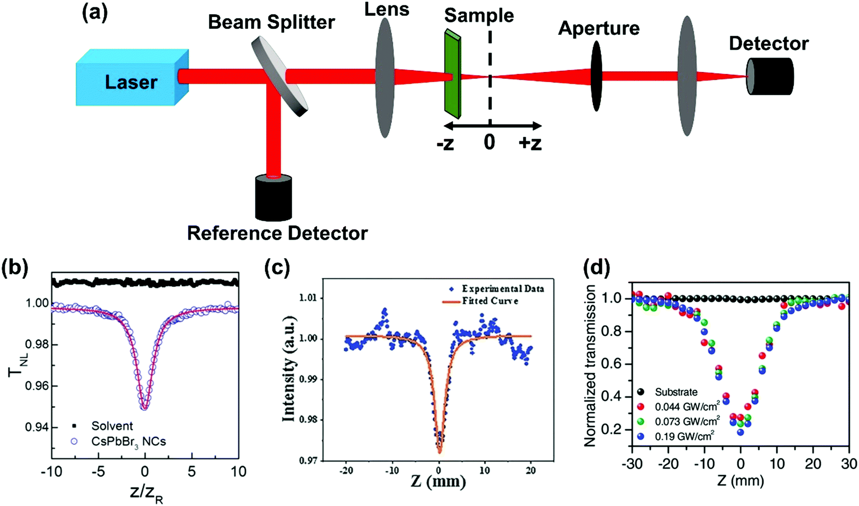 | ||
| Fig. 4 (a) The schematic diagram of the Z-scan technique; the open aperture z-scan curves measured on (b) CsPbBr3 nanocrystals in toluene solution, (c) CH3NH3PbBr3 quantum dots, and (d) a (PEA)2PbI4 (PEA = C6H5C2H4NH3) flake at different peak intensities. (b) Reprinted with permission from ref. 67. Copyright 2016 American Chemical Society. (c) Reprinted with permission from ref. 68. Copyright 2016 Wiley-VCH Verlag GmbH & Co. KGaA, Weinheim. (d) Reprinted with permission from ref. 69. Copyright 2017 Wiley-VCH Verlag GmbH & Co. KGaA, Weinheim. | ||
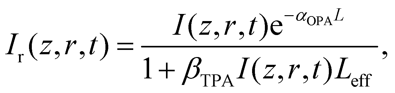
The intensity dependent nonlinear absorption coefficient α(I) can be expressed in terms of the one-photon absorption coefficient αOPA and TPA coefficient βTPA as follows:
| α(I) = αOPA + βTPAI, | (7) |
 | (8) |
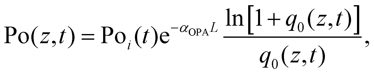 | (9) |
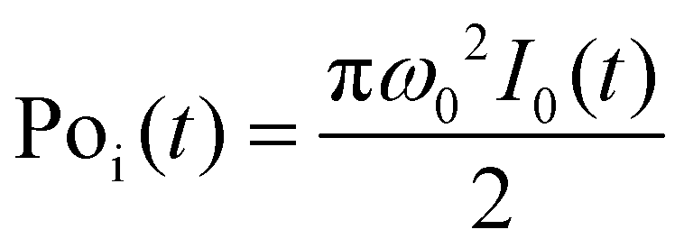 is the instantaneous input power, ω0 is beam waist at z = 0, and
  , I0 is the optical intensity at the focal point, z is the sample position and
 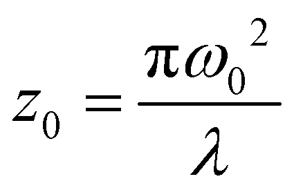 is Rayleigh range and λ is the beam wavelength.58 By fitting the experimental nonlinear absorption data, the TPA coefficient βTPA will be deduced, and the TPA cross-section σTPA can be obtained according to eqn (4). Fig. 4b–d show some examples of the experimental data together with fitting curves based on the open aperture Z-scan.
Because of its simplicity, most of the reports about TPA in halide perovskites were measured by the Z-scan method.24,58 However, the method is based on detecting small changes of the strong light beam. Such changes may have different origins other than two-photon absorption. The thermo-optical effect, self-defocusing or nonlinear scattering can be present in the measurement,24,28,59,60 which can give misleading results about the TPA coefficient.
For a colloidal nanocrystal sample, the Z-scan is normally conducted in the solution form. This means that the obtained TPA coefficient is the property of the colloidal nanocrystal solution instead of the intrinsic TPA coefficient of the nanocrystals. This might be the reason for the reported TPA cross-sections/coefficients to vary in several orders of magnitude for the same type of perovskite nanocrystals.61,62 For example, the reported TPA cross-sections of CsPbBr3 quantum dots differ by over 1 order of magnitude from 1.2 × 10⁵ GM63 up to 2.7 × 10⁶ GM64 from the Z-scan technique. It is difficult to compare the results from different reports, as the measured nanocrystal solution might (most likely) have had different concentrations. Hence, in order to compare, we have to know the concentrations or the TPA cross-section of the nanocrystals.63,65 Furthermore, a focused pulsed laser beam with high intensity has the possibility to generate the multiple exciton state within individual perovskite nanocrystals. As a result it might be difficult to determine the intrinsic single exciton TPA cross-section of the perovskite nanocrystals.66
In the Z-scan method shown in Fig. 4a, the sample's position is changed in the z-axis during the measurement. But the signal can be distorted for the samples with nonuniform thickness, nonlinearity inhomogeneities, or nonflat surfaces. To avoid such distortion, another method (shown in Fig. 5a) has been proposed, in which the sample is kept at a fixed position70 and the beam intensity is changed by using a neutral density filter wheel. Such method is not sensitive to the influence of inhomogeneity of the samples. As shown in Fig. 5a, the sample is placed at the waist of the focused laser beam and laser intensity was tuned using an attenuation slice. Some typical examples are shown in Fig. 5b–d. The normalized transmission through samples can be expressed as follows:70,71
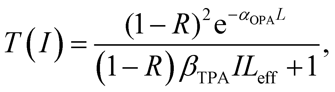 | (10) |
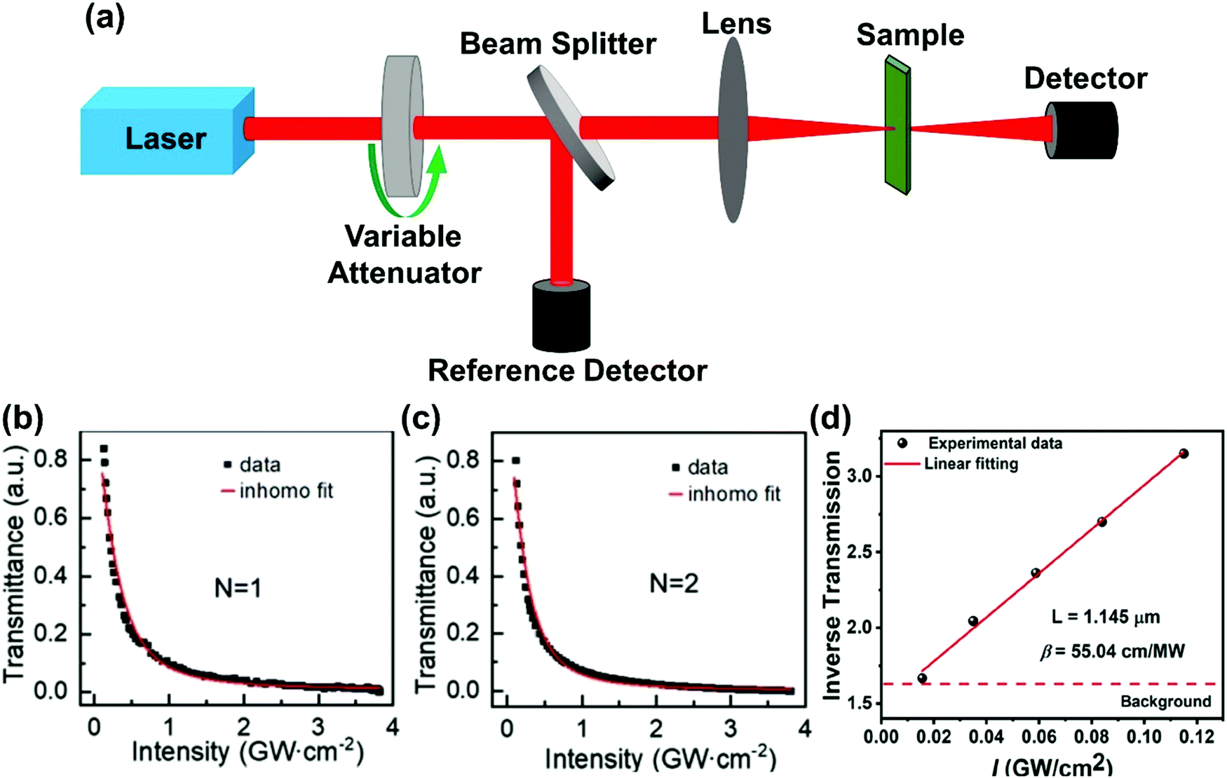 | ||
| Fig. 5 (a) The schematic diagram of nonlinear transmittance technique. (b) and (c) Nonlinear transmittance versus peak intensity of the incident laser for (n-C4H9NH3)2PbI4 (n = 1) and (n-C4H9NH3)2MAPb2I7 (n = 2) plates, respectively. (d) Inverse transmission versus incident laser peak intensity for (R-BPEA)2PbI4 (R-BPEA = (R)-1-(4-bromophenyl)ethylammonium). (b) and (c) Reprinted with permission from ref. 70. Copyright 2019 Wiley-VCH Verlag GmbH & Co. KGaA, Weinheim. (d) Reprinted with permission from ref. 71. Copyright 2021 American Chemical Society. | ||
3.2 Two-photon excited photoluminescence
An alternative way to determine the TPA cross-section is the two-photon excited photoluminescence approach, which was reported by Xu and Webb in 1996.72 In this method, the measured parameter is photoluminescence intensity instead of absorption probability (Fig. 6). The TPA cross-section can be obtained by comparing the two-photon excited photoluminescence intensity with one-photon excited photoluminescence intensities, or a reference sample with known TPA cross-section and photoluminescence quantum yield.72,73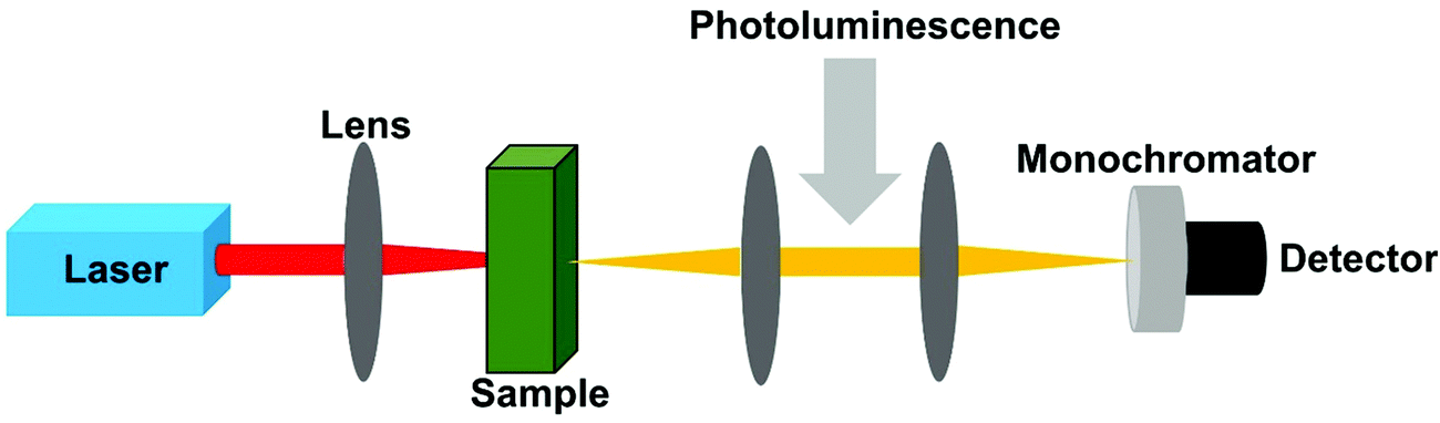 | ||
| Fig. 6 The schematic diagram of the two-photon excited photoluminescence method. | ||
This method requires precise measurement of the photoluminescence quantum yield of the materials and assumes that the materials have the same quantum yield under two-photon and one-photon excitations. This assumption usually holds but does not need to be true, due to the fact that OPA and TPA have different selection rules, and as a result, different excited states can be reached by them. The different excited states might couple to different nonradiative states.74 This may induce different photoluminescence quantum yields under one-photon and two-photon excitations. It might also be hard to find a reference sample with a known TPA cross-section and accurate photoluminescence quantum yield in the same spectral range as the fluorescence spectrum of the analyzed sample.75
3.3 Photoluminescence saturation effect method
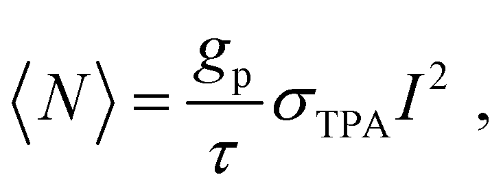
The above described two methods have been widely used for characterizing the TPA properties of perovskite samples. However, to perform such measurements in disperse systems, one of the essential requirements is to know the halide perovskite nanoparticles’ concentration beforehand. Moreover, the accurate determination of the concentration of liquid perovskite samples is not always easy and the molar extinction coefficient (or OPA cross-section) should be confirmed.66 Thus, accurate determination of σTPA of perovskite samples in dilute solution and films is challenging. Recently, Cao et al. estimated the σTPA of single particles by using the two-photon excited fluorescence saturation (TPEFS) method,75 where the photoluminescence intensity at low excitation-power densities can be well-fitted by square-power law (see Fig. 7), thus confirming the TPEF, wherein photoluminescence intensity shows saturation when the excitation power further increases due to the multiexciton Auger recombination. The photoluminescence intensity against the incident laser power profile can be fitted by using the following equations, and the σTPA can be extracted:75| F ∝ 1 − e−〈N〉, | (11) |
 | (12) |
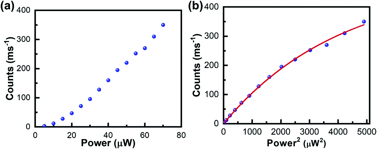 | ||
| Fig. 7 (a) Photoluminescence intensity is plotted as a function of the laser power density for single CsPbI3 NCs excited with an 800 nm light. (b) The photoluminescence intensity is plotted as a function of the square of the laser power density to show the PL saturation effect, which are fitted by eqn (11) and (12), to extract the TPA cross-section. (a) and (b) Reprinted with permission from ref. 75. Copyright 2019 AIP Publishing. | ||
To achieve the Auger recombination process, the samples have to be excited with high light intensity. This requires the samples to be stable throughout the measurement, which might be difficult for some fragile samples.
3.4 Femtosecond transient absorption
TPA cross-section can be obtained by using femtosecond transient absorption (fs-TA) spectroscopy. Here one first determines the OPA cross-section by statistical analysis of the excitation density dependent signal from fs-TA. Then one can relate the OPA signal and the TPA signal in the fs-TA; as a result one can obtain the TPA cross section with high precision.73,76–78This method ensures that the TPA cross-section of the halide perovskite samples with very weak or no photoluminescence could be obtained. Two signals in the fs-TA spectrum, the excited-state absorption (ESA) or ground-state bleach (GSB), can be used to estimate TPA cross-section. The schematic diagram of a fs-TA spectrometer is shown in Fig. 8.
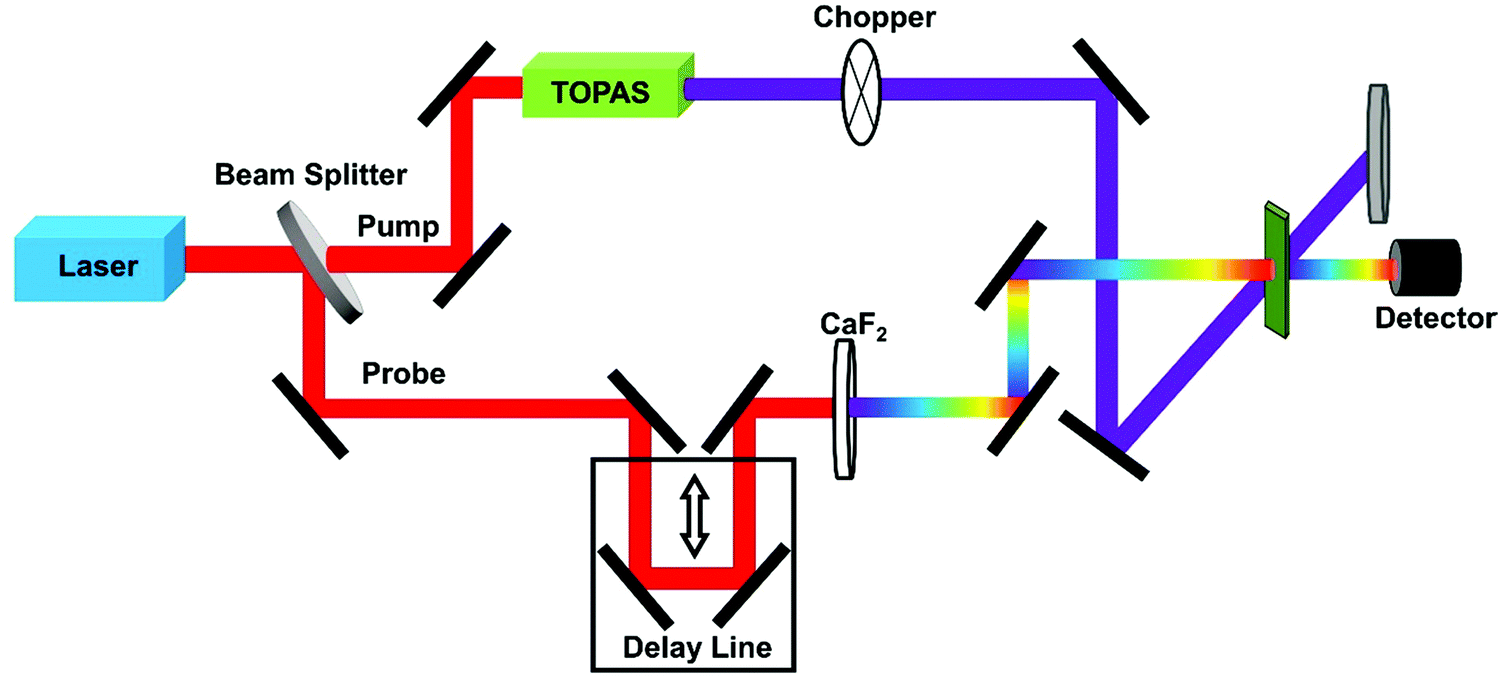 | ||
| Fig. 8 The schematic diagram of a fs-TA spectrometer. | ||
In 2001, Oulianov et al. introduced a method to estimate TPA cross-section of organic molecules in solution.73 By plotting the intensity of ESA as a function of two-photon excitation light intensity, the dependence with a slope of 2 will be obtained at low excitation intensities. The experimental conditions were kept the same for the reference and the analyzed samples; the TPA cross-section of the analyzed sample can be calculated as follows:73
 | (13) |
One could obtain TPA cross-section by comparing the ESA signals of the analyzed and reference samples. But what if we cannot find a suitable reference sample? The TPA cross-section can also be obtained by extracting the GSB information from fs-TA spectra (see Fig. 9).76,77 The normalized GSB signals are linearly proportional to the pump fluence under one-photon excitation (Iλ) and quadratically proportional to the pump fluence under two-photon excitation (I2λ) with low excitation intensity (fluence):76
 | (14) |
 | (15) |
 | (16) |
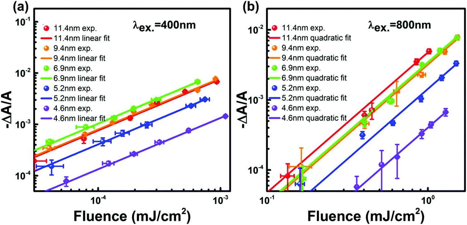 | ||
| Fig. 9 Excitation fluence-dependent GSB signal normalized with absorbance at the first exciton transition energy (−ΔA/A) for CsPbBr3 QDs with different sizes (plotted in a log–log scale under excitation at (a) 400 nm and (b) 800 nm). (a) and (b) Reprinted with permission from ref. 77. Copyright 2017 American Chemical Society. | ||
4. Photophysics in two-photon excited halide perovskites
4.1 Charge carrier dynamics
The initial charge carrier dynamics of two-photon excited halide perovskites might be different from that of one-photon excited halide perovskites due to the different excitation selection rules. Different excited states can be reached by OPA and TPA. In the case of a centrosymmetric system, the excitation selection rules for OPA and TPA are mutually exclusive. Considering a system with a gerade ground sate and the ungerade property of a dipole operator, only an ungerade state can be reached by the OPA process (Fig. 10a). For the TPA process, the intermediate state and the final excited state must be ungerade and gerade, respectively.1 The gerade final state cannot be reached by OPA as the forbidden transition. As a result, different initial excited states are reached by OPA and TPA. For example, Saouma et al., demonstrated that optical transition across the fundamental gap state of CsPbBr3 is strictly TPA forbidden due to the different excitation selection rules.79 These excited states reached by OPA or TPA might couple to different radiative/nonradiative states via different charge carrier dynamic processes, thus showing different photoluminescence.74,77,79–83 For example, in CsPbBr3 nanocrystals, with two-photon excitation, a red-shifted photoluminescence spectrum (Fig. 10b) and increased photoluminescence lifetime are observed compared with those of one-photon excitation.74 Han et al., proposed a model as shown in Fig. 10c; there are two different radiative pathways for photoluminescence in CsPbBr3 nanocrystals: excitonic and trap emission. The two different emission pathways have different excitation wavelength dependence. For the red-shifted photoluminescence spectra under two-photon excitation, the relative intensity of the trap emission is increased compared to that under one-photon excitation.65,74 This explanation is further supported by the different photoluminescence kinetics under two-photon and one-photon excitations.67,74 However, it has also been observed that photoluminescence has very similar kinetics under TPA and OPA excitation for this material.63,83 Specifically, the TPA and OPA excited PL show almost the same time-dependent decay curves indicating that excitation via either OPA or TPA relaxes to the same lowest excited states, where the radiative recombination occurs.63,83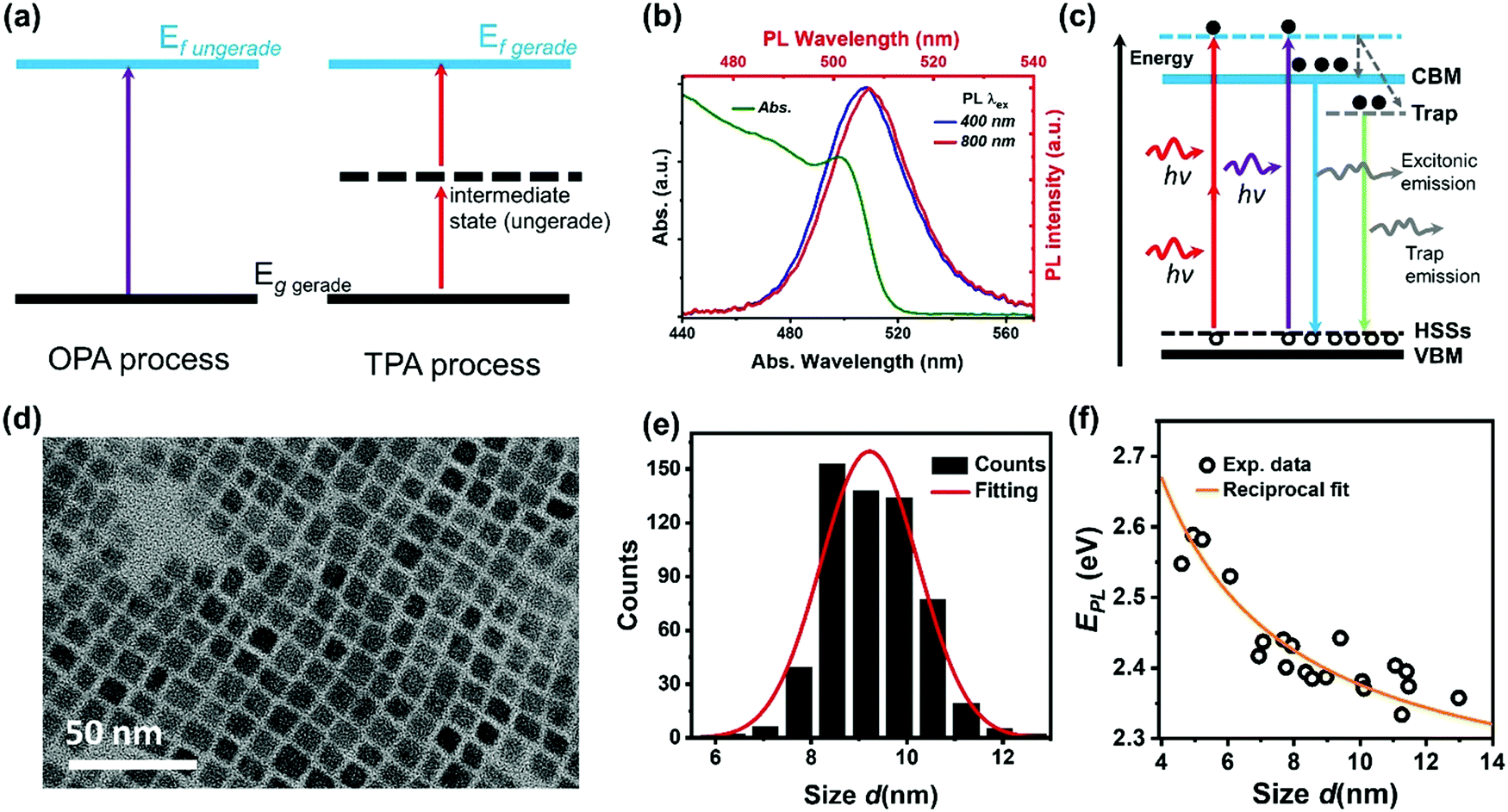 | ||
| Fig. 10 (a) Selection rules for the OPA and TPA processes, g: ground state, f: final state. (b) Steady-state absorption spectrum (green curve), one-photon excited photoluminescence (PL) spectrum (blue curve), and two-photon excited photoluminescence spectrum (red curve) of CsPbBr3 nanocrystals. (c) Schematic energy level diagram to illustrate the photoluminescence mechanism of CsPbBr3 nanocrystals with trapping and excitonic states originated in quantum confinement. CBM: conduction band minimum; ESSs: electron surface states; HSSs: hole surface states; and VBM: valence band maximum. (d) High-resolution transmission electron microscopy (TEM) image of CsPbBr3 nanocrystals. (e) Size distribution of CsPbBr3 nanocrystals. (f) Size-dependent photoluminescence energy (EPL) for CsPbBr3 nanocrystals. (b) and (f) Reprinted with permission from ref. 78. Copyright 2017 American Chemical Society. (c) Reprinted with permission from ref. 74. Copyright the Royal Society of Chemistry 2017. (d) and (e) Reprinted with permission from ref. 77. Copyright 2017 American Chemical Society. | ||
We found that the size inhomogeneity of nanocrystals can be another reason for the red-shifted photoluminescence spectrum and relatively long photoluminescence lifetime under two-photon excitation. Typically, the synthesized colloidal CsPbBr3 nanocrystals show a size distribution (Fig. 10d and e) around the average size. Because of inherent nonlinearity, the size dependence of absorption cross-section under TPA is stronger than that in OPA indicating that the different size sub-distributions of the full ensemble were excited in these two experiments.78 The larger nanocrystals show red-shifted photoluminescence compared with smaller nanocrystals (Fig. 10f), due to the size-dependent quantum confinement84 and Stokes shift.85 Moreover, larger nanocrystals have reduced quantum confinement and trapping. This explains the longer excited-state lifetime in larger nanocrystals. Under TPA excitation, larger size nanocrystals are preferably excited leading to longer excited-state lifetime and red-shifted photoluminescence.
Such red shift is more obvious in bulk single crystals compared with that in nanocrystals. As the bulk crystals can be several cm thick, the penetration depth of the excitation beam plays an important role. For example, the penetration depth of 800 nm light can extend beyond 100 μm, which is several orders longer than that of 400 nm light in MAPbBr3 bulk crystals.86 Wu et al. concluded that in bulk MAPbBr3 and MAPbI3 single crystals, their surface region has a wider bandgap compared to inside the bulk.86 A similar bandgap difference between bulk and surface has also been reported by Schuster et al.87 Under one-photon and two-photon excitation, most of the photoluminescence is generated from the surface and bulk regions, respectively. As a result, the two-photon excited photoluminescence is red-shifted compared to their one-photon excited counterpart.86
4.2 Penetration depth effect
As discussed above, TPA has a longer penetration depth compared with OPA. One-photon excited charge carriers are mostly located at the surface of halide perovskite materials, due to the limited penetration depth of the excitation light, where the generated charge carriers are ready to recombine non-radiatively/radiatively or diffuse into the materials. Two-photon excited charge carries are located inside of the materials88,89 and show different dynamics, because there exist big differences between the surface and bulk area of the materials, such as trap density, band structure and mobility. For example, in CsPbBr3 single crystals, the surface trap density is estimated to be two orders larger than that of the bulk.86 Correspondingly, the diffusion length of the surface excited charge carriers (130–160 nm) is considerably reduced compared to that of the bulk (2.6–4.3 μm).86 Furthermore, the surface region has a wider bandgap than the bulk region due to the presence of Br vacancy states on the surface.86,90The reabsorption (OPA process) plays an important role in photoluminescence under two-photon excitation, due to a large overlap between absorption and photoluminescence, large absorption coefficient and long penetration depth of two-photon excitation light. A red-shift in two-photon excited photoluminescence is widely reported in lead halide perovskites (Fig. 11a).86,89,91–96 Apart from the red-shift in photoluminescence, the PL peak under one-photon excitation exhibits a red-shift with time, while two-photon PL is time independent.93 Yamada et al. attributed the red-shifted photoluminescence under TPA to emissions from the localized states because of strong band-to-band absorption and photon re-absorption of the emitted light in the interior region.92,93 They revealed that the time-dependent PL peak shift behavior can be explained by the diffusion of photocarriers generated in the near-surface region to the interior region (Fig. 11b).93 The photoexcited carriers, which are initially generated near the surface region (∼few hundred nm penetration depth), diffuse into the interior region subsequently, thus giving rise to the PL red-shift under one-photon excitation. However, under two-photon excitation, the charge carriers are generated inside the crystal, the diffusion of photoexcited carriers does not make an observable change in photoluminescence. Instead, the observed photoluminescence under two-photon excitation might originate from defects after multiple cycles of reabsorption.93 The reabsorption effect has been further confirmed by exciting the bulk single crystals at different depths. The photoluminescence spectrum and its decay dynamics depend on the excitation-depth profile. As the excitation depth increases, the photoluminescence spectrum becomes asymmetric, the spectral peak redshifts, and the photoluminescence decay time becomes longer. These observations can be well explained by the photon recycling process (photon emission and reabsorption) in thick samples with strong band-to-band transitions and high radiative recombination efficiencies.95 Due to the photon recycling process, the two-photon excited photoluminescence shows slower decay compared to that of one-photon exited photoluminescence (Fig. 11c).86,89,93
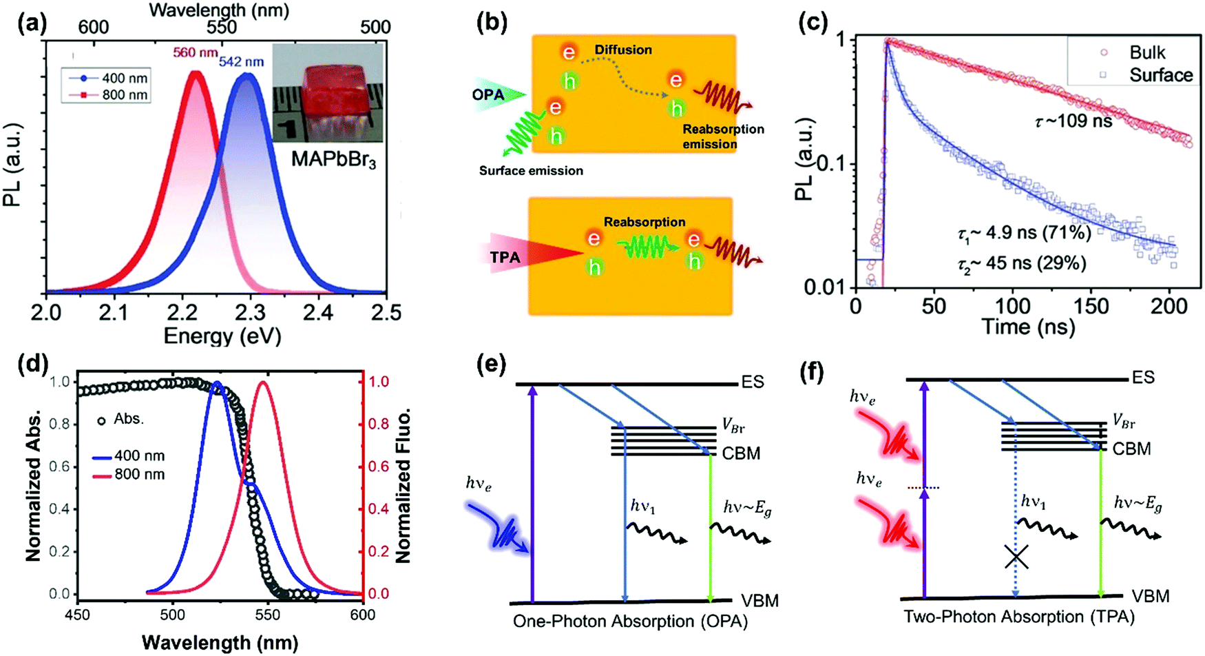 | ||
| Fig. 11 (a) The photoluminescence spectra of the MAPbBr3 single crystals with 400 nm (OPA at ≈20 μJ cm−2) and 800 nm (TPA at ≈200 μJ cm−2) excitations. Inset: image of a typical MAPbBr3 single crystal. (b) Schematic diagram of carrier diffusion and recombination processes with OPA and TPA, respectively. (c) MAPbI3 single crystal bulk emission (excited with 1200 nm, TPA, low fluence: ≈200 μJ cm−2) and surface emission (excited with 600 nm, OPA, low fluence: ≈1 μJ cm−2) dynamics. (d) Absorption and photoluminescence spectra of CsPbBr3 with 400 and 800 nm wavelength light excitation. (e) and (f): Schematic representations of the charge carrier relaxation processes under OPA and TPA, respectively; ES, excited state; VBr, Br vacancy states; CBM, conduction band minimum; and VBM, valence band maximum. (a) and (c) Reprinted with permission from ref. 86. Copyright 2016 Wiley-VCH Verlag GmbH & Co. KGaA, Weinheim. (d) Reprinted with permission from ref. 89. Copyright 2017 Wiley-VCH Verlag GmbH & Co. KGaA, Weinheim. (e) and (f) Reprinted with permission from ref. 91. Copyright 2018 Optical Society of America. | ||
Photoluminescence with double peaks (Fig. 11d) is reported repeatedly in Br-based lead perovskites.89–91,94,97 One of the two peaks is located above the bandgap energy, and the other one is located below the bandgap energy. Under two-photon excitation, the above bandgap photoluminescence peak is vanished (Fig. 11d). The origin of the above bandgap photoluminescence peak has been ascribed to Br vacancy centers.90,91 As illustrated in Fig. 11e and f, under one-photon excitation, the photoexcited carriers can be captured by the localized Br vacancy center, which binds with a hole in the valence band to form an exciton. The formed exciton recombines radiatively and yields the above-bandgap PL emission peak.91 This photoluminescence photon is re-absorbed (OPA process) by the material due to the long penetration depth in TPA. As a result, one cannot observe such above bandgap emission peak under two-photon excitation.
5. Factors influencing the two-photon absorption process
The TPA process in halide perovskites can be influenced by different factors, such as chemical composition (as shown in Fig. 2, X-site halide anion, A-site cation, and B-site (Pb) metal cation), structure, size, morphology, and external physical environment. These factors offer us many possibilities to tune their TPA properties in a wide range. In this part we summarize the TPA properties (including TPA cross-section, coefficient, and photoluminescence) of halide perovskites.5.1 Chemical composition
The chemical diversity of halide perovskites provides the possibility to tune their properties via different chemical compositions. For example, different chemical compositions can change the bandgap, phase structure and morphology of halide perovskites, which directly affect the TPA properties of halide perovskites.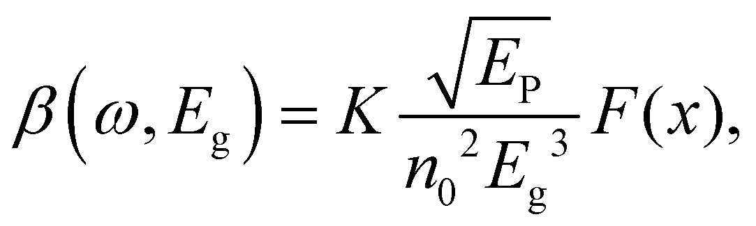 | (17) |
 | (18) |
One can see from eqn (17) that the TPA coefficient is bandgap dependent. The two-band model is expected to be able to describe the TPA coefficient of the three-dimensional APbX3 lead halide perovskite single crystals. Because they have well-defined structures, clean bandgap, low defect densities, and large dimensions in macroscopic scale.19 The bandgap of lead halide perovskites can be changed using the X-site halide anion (Fig. 2d). Hence, halide anion mixing is one of the most effective strategies for tailoring the TPA properties of lead halide perovskites.106,107 Saouma et al. demonstrated that the TPA coefficients of MAPbX3 single crystals show bandgap dependence by changing the X-site halide anion.105 To visualize the bandgap dependence, the TPA coefficient can be scaled by  , and we plot the scaled TPA coefficients versus bandgap in Fig. 12a. As one can see, most of the reported values for single crystals follow the Eg−3 dependence as predicted by the two-band model. Furthermore, several groups also reported that the TPA coefficients can be tuned by changing the X-site halide anions in MAPbX3 and CsPbX3 films and nanocrystals.65,105–110
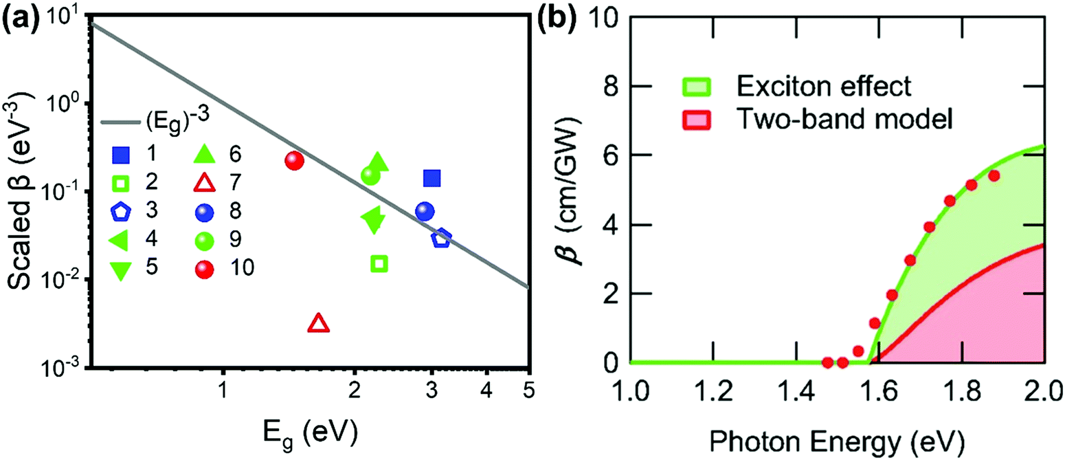 | ||
Fig. 12 (a) log−log plot of the scaled TPA coefficient,  , versus bandgap energy generated with a single scaling parameter K = 4200. The grey line is Eg−3. This implies that the TPA coefficients of the halide perovskites follow the universal bandgap scaling within the two-band model. Data points 1–7 are from ref. 59 and 99–104, respectively, data points 8–10 are from ref. 105. (b) Excitation-energy dependences of β. Filled red circles are experimental data. The green solid line is the fitting result considering the exciton effect. The green area represents the contribution from the exciton effect, and the red area represents the contribution from the two-band model. (b) Reprinted with permission from ref. 101. Copyright American Physical Society 2019. , versus bandgap energy generated with a single scaling parameter K = 4200. The grey line is Eg−3. This implies that the TPA coefficients of the halide perovskites follow the universal bandgap scaling within the two-band model. Data points 1–7 are from ref. 59 and 99–104, respectively, data points 8–10 are from ref. 105. (b) Excitation-energy dependences of β. Filled red circles are experimental data. The green solid line is the fitting result considering the exciton effect. The green area represents the contribution from the exciton effect, and the red area represents the contribution from the two-band model. (b) Reprinted with permission from ref. 101. Copyright American Physical Society 2019. | ||
However, the two-band model did not well describe the excitation energy dependent TPA coefficient of MAPbCl3 single crystals.100 The reason for this might be the absent of coulomb interaction or exciton effect in the two-band model, as the reported exciton binding energy of MAPbCl3 can be 41 meV, which is much larger than thermal energy at room temperature.96 Hence, Ohara et al. incorporated the exciton effect in the two-band model to describe the excitation energy dependent TPA coefficient of MAPbCl3 single crystals. As shown in Fig. 12b, the energy dependent TPA coefficient can be well described by the two-band model with exciton effect. The match between experimental results and theoretical model indicates that the exciton effect can enhance the TPA in MAPbCl3 and other halide perovskite materials. In particular, in halide perovskite nanomaterials, the exciton effect is enhanced by quantum confinement. We will discuss this point in the coming sections.
However, there are only limited studies about how the A-site cations influence the TPA properties for halide perovskite with the APbX3 structure. It is not logical to compare the results from different studies for materials with different sizes/morphologies or measurement methods with different laser pulse widths, as these factors can alter the TPA properties and processes. Here we compare the TPA coefficient of APbCl3 and APbBr3 (A = Cs or MA) single crystals measured with fs-laser pulses. As shown in Fig. 13a and Table 1, the TPA coefficients of MA based single crystals are larger than those of Cs based single crystals59,100 under similar experimental conditions. Such a similar trend has been reported in CsPbBr3 and MAPbBr3 nanocrystals as well.68 This can be ascribed to the organic cation MA having changeable orientation under light irradiation, which may assist the TPA process (Fig. 13b).68
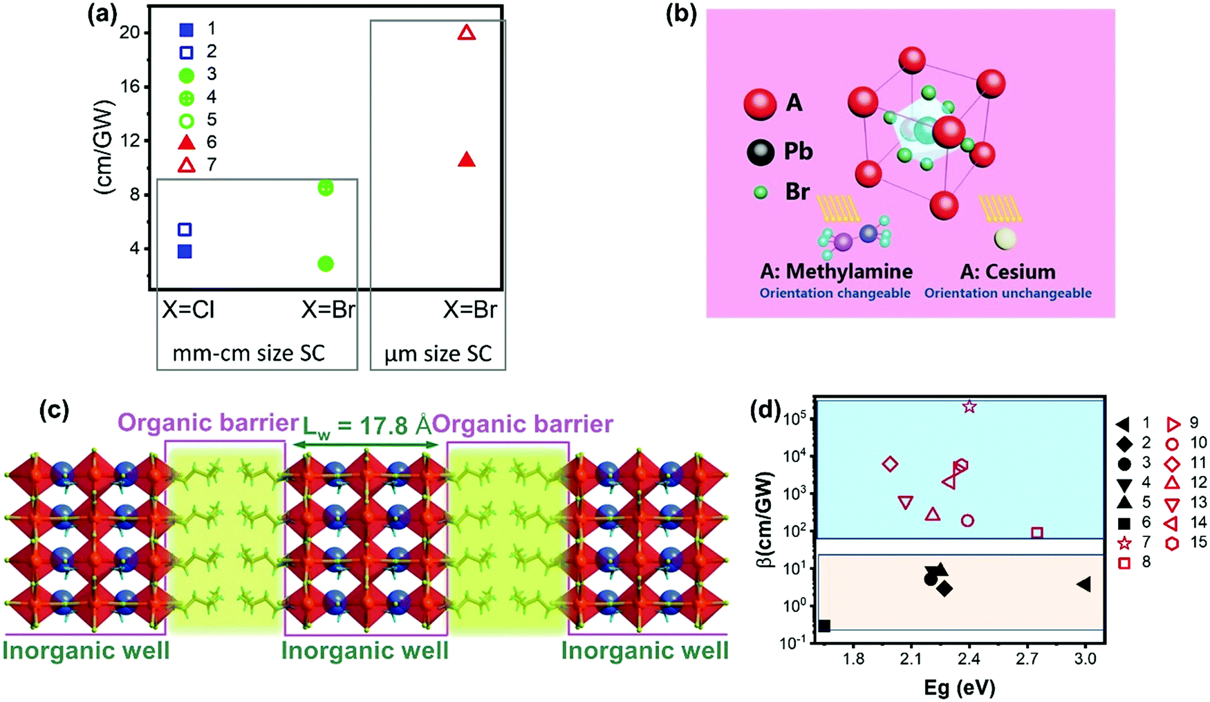 | ||
| Fig. 13 (a) TPA coefficient β of CsPbCl3 (filled square), MAPbCl3 (empty square), CsPbBr3 (filled circle), and MAPbBr3 (empty circle and circle with a cross) single crystals, and CsPbBr3 (filled triangle) and MAPbBr3 (empty triangle) microcrystals. The x-axis represents different halides (Cl, and Br), and the y-axis represents the TPA coefficient. Data points 1–7 are from ref. 59, 89, 99–101, 103 and 113, respectively. (b) Schematic view of a perovskite with two different A-site cations. (c) Diagram of the quantum-well motif with alternate arrays of inorganic perovskite frameworks (well) and organic cation bilayers (barrier). (d) TPA coefficient of 3D perovskite (black filled) and 2D perovskites (red empty). Data points 1–15 are from ref. 59, 69, 70, 99, 100, 102–104, 112, 114 and 115, respectively. (b) Reprinted with permission from ref. 68. Copyright 2016 Wiley-VCH Verlag GmbH & Co. KGaA, Weinheim. (c) Reprinted with permission from ref. 115. Copyright 2020 Wiley-VCH Verlag GmbH & Co. KGaA, Weinheim. | ||
The cations can be replaced with bulky organic cations and low-dimensional perovskite structures such as two-, one- and 0-dimensional structures can be formed. Particularly, for two-dimensional perovskite structures, the layered structure that is formed by inorganic layers and organic cation layers can be regarded as the quantum structure, in which the organic layer acts as a barrier and the inorganic layer acts as well (Fig. 13c). As the energy bandgap of the organic layer is larger than that of the inorganic layer, while the dielectric constant of the organic layer is smaller than that of the inorganic layer.69 Due to the specific quantum and dielectric confinement, the charge-carriers can be confined in the inorganic layers and the light–matter interaction is enhanced due to the confinement effects.112 As a result, the TPA can be enhanced in low dimensional perovskite structures.116Fig. 13d shows the TPA coefficients of representative two-dimensional and three-dimensional halide perovskite materials. The TPA coefficients of three-dimensional halide perovskite single crystals are less than 10 cm GW−1, whereas the TPA coefficients of two-dimensional halide perovskite flakes vary in a wide range (from 90 to over 2 × 105 cm GW−1) from different reports. Nevertheless, two-dimensional halide perovskite materials show a much higher TPA coefficient compared to three-dimensional halide perovskite materials.
 | ||
| Fig. 14 (a) Crystal structure of dopped APbX3 lead halide perovskites. (b) Schematic showing the mid-gap states arising due to doping in APbX3 halide perovskites. (c) Wavelength-dependent TPA cross-sections of CsPbI3 perovskite NCs (pure and doped with Zn2+). (d) Crystal structure of lead-free double-perovskite Cs2AgBiBr6 viewed along the a-axis. (e) Crystal structure of lead-free zero-dimension perovskite (C4H14N2)2In2Br10 viewed along the a-axis. The organic cations intercalate between the isolated polyhedrons. (a) and (c) Reprinted with permission from ref. 121. Copyright 2020 American Chemical Society. (b) Reprinted with permission from ref. 123. Copyright 2019 American Chemical Society. (d) Reprinted with permission from ref. 124. Copyright 2018 Wiley-VCH Verlag GmbH & Co. KGaA, Weinheim. (e) Reprinted with permission from ref. 125. Copyright 2019 Wiley-VCH Verlag GmbH & Co. KGaA, Weinheim. | ||
The lead element in halide perovskites can be replaced completely by other metal elements with low-toxicity, such as Sn2+, Bi3+, Sb3+, Ag+, In3+ and Ge2+.126–128 Some of these lead-free halide perovskites show different crystal structures from the typical lead halide perovskites, namely, double perovskite with general formula A2M(I)M′(III)X6 or vacancy-ordered low-dimensional layered perovskite structures (Fig. 14d and e).124,125 The increased polarity and decreased dimensionality can enhance the TPA in these perovskite materials. However, currently most research is focused on their OPA process for photovoltaic applications, and the study on TPA is still lacking.
5.2 Size effect
The size of halide perovskite materials can vary by 7 orders of magnitude (e.g. from cm-sized crystals down to nm-sized crystals, Fig. 15a). When the size of the material is close to the exciton Bohr radius, the quantum confinement strongly influences the TPA process. As a result, the TPA can be enhanced in nm-size perovskites.69 As shown in Fig. 15b, we summarized the TPA coefficients of two typical halide perovskites (CsPbBr3 and MAPbBr3) with different crystal sizes (from cm to nm). The reported TPA coefficients of these lead halide perovskite nanocrystals show a broad distribution (from less than 1 to over 2000 cm GW−1). Nevertheless, the nanocrystals still show a larger TPA coefficient than the large size crystals. The enhancement might be due to the quantum confinement in the nanocrystals.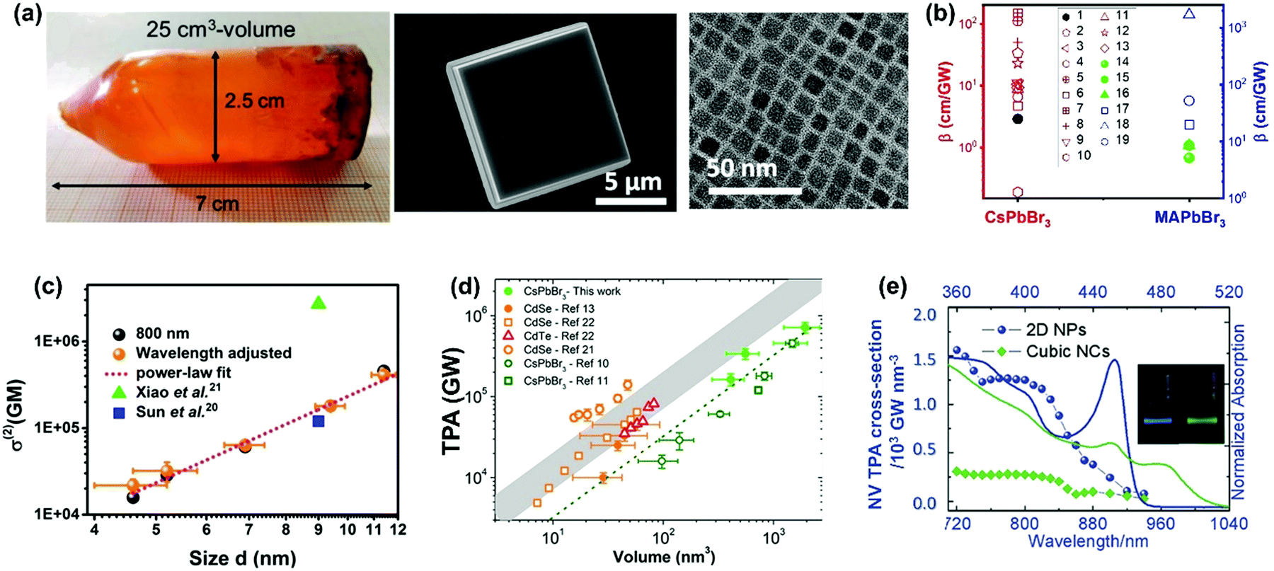 | ||
| Fig. 15 (a) CsPbBr3 crystals with different sizes (from few cm to nm). (b) TPA coefficients of CsPbBr3 and MAPbBr3 crystals from several cm to nm in size, filled black circle is CsPbBr3 single crystals of cm size, red empty shapes are CsPbBr3 nanocrystals, green filled circle and triangle are MAPbBr3 single crystals of cm size, blue empty shapes are MAPbBr3 nanocrystals. Data points 1–19 are from ref. 59, 63, 65, 67, 68, 77, 83, 89, 100, 102, 103, 106, 113 and 129–132, respectively. (c) Size-dependent TPA cross-section of CsPbBr3 nanocrystals. (d) Volume dependence of TPA cross-section of CsPbBr3 nanocrystals. (e) Volume-normalized TPA and linear absorption spectra of 2D NPs and cubic NCs, plotted over two- and one-photon energy. The inset is the picture of PL emission of 2D NPs and cubic NCs. (a) Reprinted with permission from ref. 100. Copyright 2017 Wiley-VCH Verlag GmbH & Co. KGaA, Weinheim. (c) Reprinted with permission from ref. 77. Copyright 2017 American Chemical Society. (d) Reprinted with permission from ref. 133. Copyright 2018 American Chemical Society. (e) Reprinted with permission from ref. 129. Copyright 2018 Wiley-VCH Verlag GmbH & Co. KGaA, Weinheim. | ||
We found that TPA cross-section of CsPbBr3 nanocrystals follows a power law dependence on nanocrystal size with an exponent 3.3 (Fig. 15c).77 In order to exclude the size effect from the nanocrystals, we normalized the TPA cross-section with the volume and obtained the TAP coefficient. When normalized by volume, the TPA coefficient of CsPbBr3 nanocrystals does not show strong size dependence. There is no big difference between nanocrystals with size larger or smaller than the Bohr radius (7 nm).134 This indicates that quantum confinement does not have any significant effect on TPA in CsPbBr3 nanocrystals in the size range from 4.6 to 11.4 nm. This might be due to the enhanced size selection under two-photon excitation: the larger size nanocrystals are preferably excited.78 Because of inherent nonlinearity, the size dependence of absorption cross-section under TPA is stronger than that under OPA.77,78 Consequently, larger size NCs are preferably excited. As a result, the quantum confinement cannot be observed for the nanocrystals with an average size smaller than the Bohr radius. In addition, Nagamine et al. presented a comprehensive study of TPA for CsPbBr3 nanocrystals with sizes varying from 7.4 to 12.5 nm and observed that the TPA cross-section followed a nearly linear dependence with the volume of quantum dots (Fig. 15d).133 These results suggest that there is a positive correlation between the TPA cross-section and size that is close to the Bohr radius. Thus, the following interesting questions can be raised: what is the threshold size for quantum confinement effect to influence the TPA properties, and how can we confirm this threshold size? For CsPbBr3 nanocrystals of ∼4 nm size, Butkus et al. observed strong quantum confinement effects such as state focusing, state-to-state transitions, and strong bandgap renormalizations in fs-TA spectra under OPA. Could 4 nm be the threshold size for quantum confinement effect to influence the TPA properties also? It has been reported that nanoplates with ∼2 nm thickness show a larger volume-normalized (VN) TPA cross-section compared to cubic nanocrystals in He and Zhao et al.'s work.129,135 The enhanced TPA in nanoplates has been ascribed to the quantum confinement effect.129,135 This indicates the threshold size for quantum confinement to influence TPA might be between 2 nm and 4.6 nm. Further study is needed to get the exact value.
He and co-workers observed the influence of the quantum confinement on TPA properties of CsPbBr3 nanocrystals.129 They compared the TPA cross-section of CsPbBr3 nanoplates and cubic nanocrystals. The thickness of the nanoplates used in the experiment is around 1.8 nm, which corresponds to three-unit cells. The nanoplates show a much larger TPA cross-section than cubic nanocrystals in the 720–900 nm wavelength range (Fig. 15e), and the TPA coefficient of nanoplatelets (50.3 cm GW−1) is about 5 times that of cubic nanocrystals (10.9 cm GW−1).129 They explained that the enhanced TPA in 2D nanoplatelets is due to the increased transition dipole moments and band mixing with a strong confinement effect. A similar enhancement has also been reported in CsPbBr2.7I0.3 and CsPbCl3 nanoplatelets.120,135
5.3 Morphology
Halide perovskites can be prepared with different morphologies (Fig. 16),22,136–140 such as large single crystals, films, microcrystals, microwires, microplatelets, nanorods, nanoplatelets, nanosheets, and cubic nanocrystals, which can influence the TPA process. For example, the localized electric field and the sub-bandgap state density can be different for different morphologies.102,131 As shown in Fig. 17a, the reported TPA coefficient of film morphology is higher than that of the single crystal counterparts in CsPBr3, MAPbBr3 and MAPbCl3 perovskites. This might be due to the increased defect density in the film, which acts as sub-bandgap states and enhances the TPA process. This has been reported in different types of perovskite materials.141–145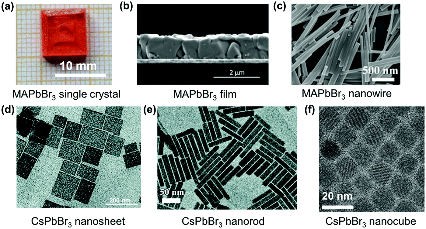 | ||
| Fig. 16 Different morphologies of perovskite materials: (a) optical image of MAPbBr3 single crystals of cm-size. (b) Scanning electron microscope (SEM) image of polycrystalline MAPbBr3 film grown on ITO-coated glass. (c) SEM images of MAPbBr3 nanowires. (d) TEM image of CsPbBr3 nanosheets. (e) TEM image of CsPbBr3 nanorods. (f) TEM image of CsPbBr3 nanocubes. (a) Reprinted with permission from ref. 138. Copyright 2017, Springer Science Business Media New York. (b) Reprinted with permission from ref. 140. Copyright 2016 Wiley-VCH Verlag GmbH & Co. KGaA, Weinheim. (c) Reprinted with permission from ref. 136. Copyright 2017 Wiley-VCH Verlag GmbH & Co. KGaA, Weinheim. (d) Reprinted with permission from ref. 139. Copyright the Royal Society of Chemistry 2016. (e) Reprinted with permission from ref. 137. Copyright the Royal Society of Chemistry 2019. | ||
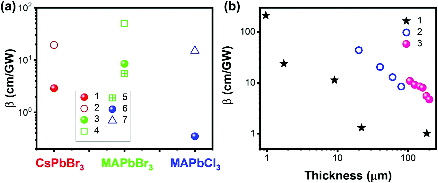 | ||
| Fig. 17 (a) TPA coefficients of CsPbBr3, MAPbBr3 and MAPbCl3 single crystals (filled balls) and film (empty shapes) form. Data points 1–7 are from ref. 69, 100, 101, 103, 110 and 146, respectively. (b) Thickness dependent TPA coefficients of halide perovskites. Data sets 1–3 are from ref. 69, 70 and 80, respectively. | ||
Krishnakanth et al. demonstrated the broadband TPA properties of CsPbBr3 films made from nanocubes and nanorods; they found that the TPA coefficients of nanocubes were higher than those of nanorods at three different wavelengths.131 However, the influence of the volume on the nanocubes and nanorods, as well as the thickness of films, was not further discussed in this work. Zhao et al. performed a comparison study of nonlinear optical properties of CsPbBr2.7I0.3 perovskites between the 2D nanoplatelets and cubic nanocrystals;135 it is found that the volume-normalized (VN) TPA cross-section shows significant geometry dependence, where the maximum VN σTPA of 2D nanoplatelets is 4 times larger than that of cubic nanocrystals because of a strong quantum confinement effect. This is also confirmed by He et al. (Fig. 15e),129 as discussed in the section above.
However, the defects might inhibit the TPA process as well. For example, Li and co-workers reported that the TPA coefficient of CH3NH3PbI3 perovskite nanosheets decreases with the increase in nanosheet thickness, which is mainly due to the defect states.147 For the thicker nanosheets, more defects in the crystal would induce more scattering and energy loss, which results in a lower TPA coefficient.147 Liu and co-workers observed a similar sample thickness dependent TPA coefficient in (PEA)2PbI4 flakes. As shown in Fig. 17b, the TPA coefficient decreases as the sample thickness increases from 0.95 μm to 200 μm. They attributed this to the light absorption by the sample (self-absorption). As the laser beam propagates along the sample, the optical intensity will reduce gradually due to the OPA and TPA of the sample, which in return results in a reduced nonlinear absorption. As a result, the measured TPA coefficient decreases as the sample thickness increases. When the thickness reaches over 10 μm, the TPA coefficient tends to become similar to that of bulk MAPbI3 single crystals.69,104 A similar effect has also been observed in CsPbBr3 perovskite nanosheets (Fig. 17b)80 and (n-C4H9NH3)2PbI4/(n-C4H9NH3)2(CH3NH3)Pb2I7 heterostructures (Fig. 17b).70
5.4 Enhance two-photon absorption
The TPA process can be tailored by changing the intrinsic properties of halide perovskite as discussed above. However, the nonlinear nature of TPA requires the excitation intensity to be several orders of magnitude higher than that of the OPA process,148 whereas the high excitation intensity limits the application of TPA in fluorescence bioimaging and other nonlinear optoelectronic device applications. Hence, some other strategies were proposed to enhance the TPA and its photoluminescence.To enhance TPA, one straight forward way is to enhance the TPA coefficient of the material, as we have discussed most of them in the above sections. Moreover, Wang et al. found that it is possible to increase the TPA of two-dimensional layer halide perovskites ((n-C4H9NH3)2PbI4 and (n-C4H9NH3)2(CH3NH3)Pb2I7) by introducing a heterostructure between the two materials (Fig. 18a and b). They reported the heterostructure has a giant TPA coefficient (44 × 103 cm GM−1).70 And they attributed the enhancement to the thin thickness of the (n-C4H9NH3)2(CH3NH3)Pb2I7 layer, the efficient nonradiative energy transfer and excellent crystalline quality.70 Chen et al. developed a core–shell structure (Fig. 18c) to enhance the TPA cross-section of lead halide perovskite nanocrystals. The 3D MAPbBr3 is the core and 2D (OA)2PbBr4 (OA: octylammonium) is the shell. The TPA cross-section can be enhanced over 7 times (Fig. 18d). The shell layer can increase the TPA cross-section in different ways: acting as an antenna-like effect, introducing an internal electric field and dielectric confinement (local field effect) resulting from the relatively large difference between the dielectric constants of the core and the shell.83 Such TPA enhancement with the shell layer might play a role in the CsPbBr3 quantum dots modified by hydrophobic zeolites,149 in which the CsPbBr3 quantum dots with zeolite coating show a very high TPA coefficient (3.0 × 103 cm GW−1).
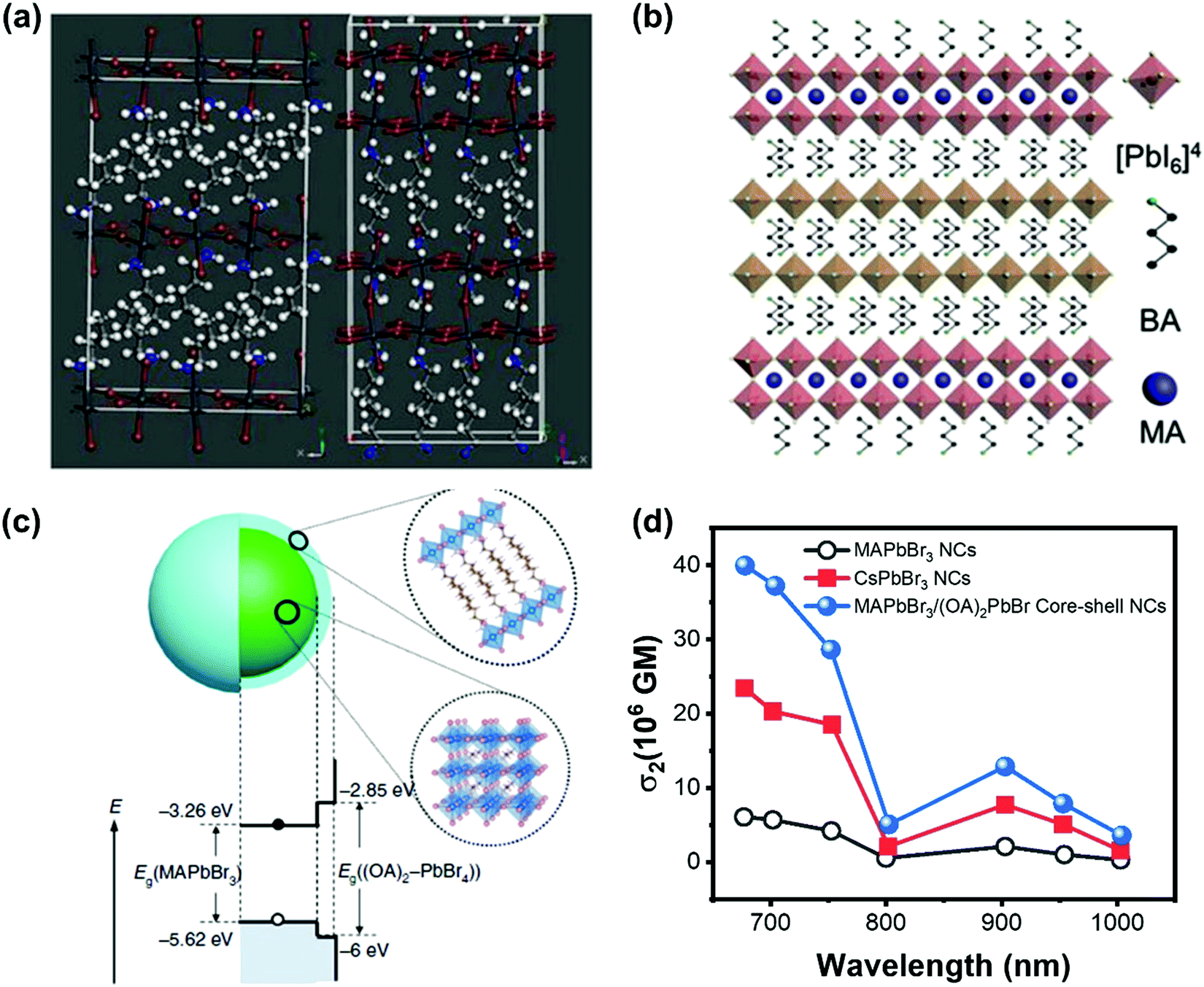 | ||
| Fig. 18 (a) Schematic illustration of the crystal structures of (n-C4H9NH3)2PbI4 and (n-C4H9NH3)2(CH3NH3)Pb2I7. (b) Schematic illustration of (n-C4H9NH3)2PbI4/(n-C4H9NH3)2(CH3NH3)Pb2I7 heterostructure. (c) Schematic illustrating the core–shell multidimensional perovskite nanocrystals (NCs) with 3D MAPbBr3 as the core and 2D (OA)2PbBr4 as the shell, and their type-I energy level alignment. (d) TPA cross-section spectra of the MAPbBr3, MAPbBr3/(OA)2PbBr4 and CsPbBr3 NCs in the wavelength range 675–1000 nm. (a) and (b) Reprinted with permission from ref. 70. Copyright 2019 Wiley-VCH Verlag GmbH & Co. KGaA, Weinheim. (c) Reprinted with permission from ref. 83. Copyright the authors. The data in (d) are from ref. 83. | ||
Moreover, owing to the nonlinearity of TPA, the two-photon excited photoluminescence can be enhanced extrinsically by enhancing light–matter interaction, such as concentrating the excitation electromagnetic field,151 near-field enhancement,150,152 and surface plasmon–exciton coupling.153,154 We took the advantage of high local light intensities in photonic nanostructures to enhance the TPA in CsPbBr3 quantum dots. Here, we investigated the two-photon-excited photoluminescence of CsPbBr3 perovskite quantum dots on a silicon photonic crystal slab (Fig. 19a–c).150 By systematic excitation of optical resonances using a pulsed near-infrared laser beam, we observed an enhancement of two-photon-pumped photoluminescence by more than one order of magnitude when compared to using a bulk silicon film (Fig. 19d).150 Liu et al. fabricated a perovskite-microsphere hybrid dielectric structure as shown in Fig. 19e.151 They reported the TPA induced photoluminescence of the perovskite that can be enhanced over 100-fold in the dielectric structure (Fig. 19f), due to the concentrated excitation electric field at the microspheres.151 The surface plasmon–exciton coupling can enhance the TPA induced photoluminescence of CsPbBr3 nanocrystals, which was demonstrated by Cai et al.153 In their work, they coated CsPbBr3 nanocrystals with PMMA on a substrate with a Ag nanostructure. A two-fold TPA induced photoluminescence was observed, and the photoluminescence decay was accelerated due to the surface plasmon–exciton coupling effect. Fan et al. constructed a perovskite metasurface: a polymer grating on an 80 nm MAPbBr3 perovskite film (Fig. 20a and b).148 They observed a giant enhancement of TPA induced photoluminescence from the perovskite metasurface. The enhancement factor is estimated to be about 106. The efficiency of the nonlinear TPA process can become comparable to the efficiency of the linear OPA process. As shown in Fig. 20c, at the same excitation intensity, one can observe a similar photoluminescence intensity under TPA and OPA. Furthermore, the enhanced TPA induced photoluminescence process ensures that the threshold of two-photon stimulated emission is only 2.7 times higher than the linear one. They attributed the giant enhancement effect to the local-field enhancement in the metasurface, a significant increase of an overlap between stimulated emission and excitation modes and access the OPA transition forbidden transitions in lead–halide perovskites.148
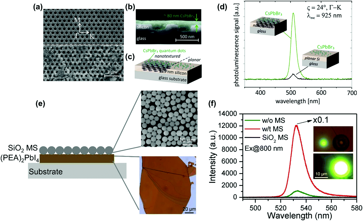 | ||
| Fig. 19 (a) SEM image of the silicon nanohole array layer (thickness: 115 nm, hexagonal lattice constant: 600 nm, hole diameter: 365 nm) on a glass substrate without (upper part of the image) and with (lower part of the image) drop-casted CsPbBr3 perovskite quantum dot coating. White arrows indicate the high symmetry directions of the hexagonal lattice of the photonic nanostructure. The scale bar applies to both SEM image parts. (b) Cross section SEM image with the quantum dots coating illustrated in green. (c) Schematic diagram of the sample geometry with the quantum dots deposited on nanotextured (left part) and planar (right part) silicon layer as reference (not to scale). (d) Photoluminescence spectra for excitation at λexc = 925 nm and an incident angle of ϑ = 24° in Γ–K direction (indicated in part (a) by a dashed line and circles) either with the excitation beam hitting CsPbBr3 quantum dots located on a nanotextured area (green curve) or a planar area (black curve) of the silicon layer. (e) (PEA)2PbI4 perovskite–SiO2 microsphere (MS) hybrid dielectric structure. (f) Two-photon pumped photoluminescence spectra of (PEA)2PbI4 flakes with (denoted as w/t in figure) and without (denoted as w/o in the figure) the SiO2 microsphere (denoted as MS) and reference SiO2 microsphere. Insets: two-photon pumped photoluminescence images without (top panel) and with (bottom panel) SiO2 microspheres. (a)–(d) Reprinted with permission from ref. 150. Copyright 2018 American Chemical Society. (e) and (f) Reprinted with permission from ref. 151. Copyright 2018 Wiley-VCH Verlag GmbH & Co. KGaA, Weinheim. | ||
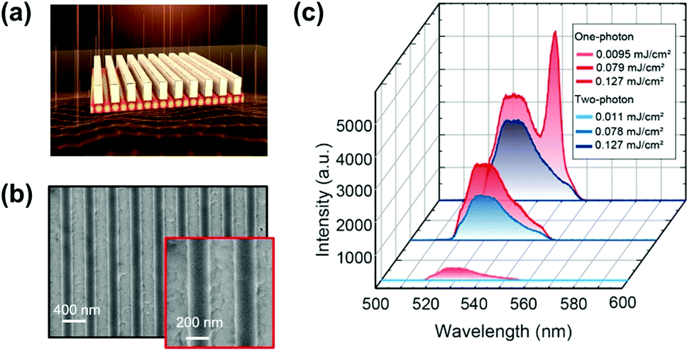 | ||
| Fig. 20 (a) Design of perovskite metasurfaces, which consists of a polymer grating on an 80 nm perovskite film. The lattice spacing filling factor and thickness of the grating are l = 395 nm, FF = 0.5, and h = 200 nm, respectively. (b) Top-view SEM images of the fabricated metasurfaces. (c) Emission spectra under one-photon and two-photon excitation at three pump fluences. (a)–(c) Reprinted with permission from ref. 148. Copyright 2021 American Chemical Society. | ||
6. Applications of two-photon absorption
In this section, we summarize the recently established applications of TPA in halide perovskites: up-conversion laser, sub-bandgap photodetection, bioimaging,25 phase modulated two-photon excited photoluminescence/photocurrent mapping, and optical limiting.26,276.1 Up-conversion laser based on two-photon absorption
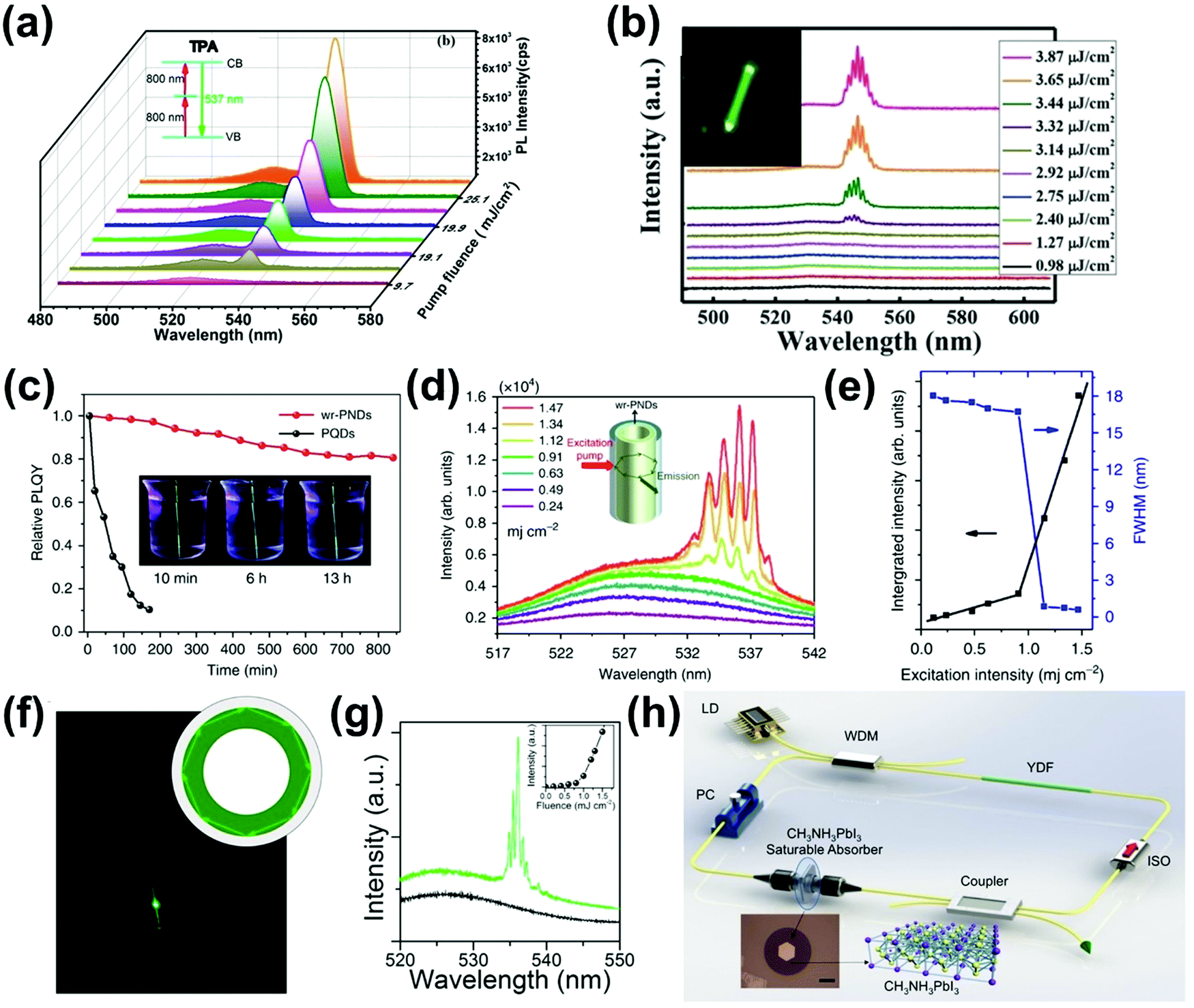
For most conventional lasers with the OPA process, the lasing photons have a lower energy than the pumping light. However, with the TPA process, the laser output photons can have a higher energy than the pumping light. Here we refer this process as up-conversion laser based on TPA. Up-conversion laser offers a simple and efficient alternative to nonlinear optical techniques for converting near-infrared and infrared laser output to the visible and near ultraviolet regimes.155 Two-photon excited amplified spontaneous emission of halide perovskites is promising for their use as gain media in up-conversion lasers.63 Their chemical diversity offers the possibility to engineer up-conversion efficiency and amplified spontaneous emission threshold.156,157A laser is a coherent light source that consists of a gain medium, an optical cavity and a pump source.160 The gain medium emits and amplifies the light via stimulated emission. The development of a new gain medium is important for further progress in laser technology. The halide perovskites are a new class of photoluminescence materials with a high TPA coefficient and widely tailorable bandgaps, showing great potential as a gain medium for two-photon pumped lasers.156 In 2015, Pan et al. reported TPA induced ultra-stable amplified spontaneous emission (ASE) from solution processed CsPbBr3 quantum dots (Fig. 21a) with a threshold of 12 mJ cm−2.158 Since then extensive research has been devoted to exploring the halide perovskite materials for two-photon pumped lasing applications. The subsequent report demonstrated two-photon pumped micro-lasers from halide perovskite CH3NH3PbBr3,159 in which periodic lasing peaks around 546 nm under optical excitation at 800 nm were observed (Fig. 21b). They found that the quality-factor (Q factor) is about 682 and the corresponding threshold is about 674 μJ cm−2.
 | ||
| Fig. 21 (a) Pump-fluence relationship determined for the treated CsPbBr3 quantum dot film under two-photon excitation. (b) Emission spectra of perovskite CH3NH3PbBr3 microwires under different pumping intensities. The inset shows the fluorescence microscope image at 3.65 μJ cm−2. (c) Relative photoluminescence quantum yields (PLQYs) of the laser devices (measured in an integrating sphere under 375 nm laser excitation) based on perovskite quantum dots (PQDs, black dots) and water-resisted PQDs@SiO2 nanodots (wr-PNDs, red dots), which were immersed in water for different periods of time. The insets are the photographs of the wr-PND-based laser in water taken at different time periods under UV light illumination. (d) Emission spectra and (e) integrated intensity and emission full width at half maximum (FWHM) for the wr-PND-based laser immersed in water for 13 h, as a function of pumping intensity under 800 nm fs laser excitation. The inset in (d) sketches the capillary-like microcavity laser device. (f) Photoluminescence image of a lasing cylindrical microcapillary tube incorporated with CsPbBr3 nanocrystals. Inset: the whispering gallery modes supported by the microring resonator. (g) Two-photon-pumped photoluminescence spectra recorded with excitation fluence below (0.7 mJ cm−2, black) and above the threshold (1.0 mJ cm−2, green), respectively. The inset shows the emission intensity as a function of excitation fluence. (h) Schematic diagram of the ring cavity of the mode-locked fiber laser. LD: 974 nm laser diode; YDF: ytterbium-doped fiber; WDM, wavelength division multiplexer; ISO: 1064 nm polarization independent isolator; and PC: polarization controller. Inset: optical image of perovskite nanosheet covering on the core area of the fiber endfacet. (a) Reprinted with permission from ref. 158. Copyright 2015 American Chemical Society. (b) Reprinted with permission from ref. 159. Copyright 2015 Wiley-VCH Verlag GmbH & Co. KGaA, Weinheim. (c)–(e) Reprinted with permission from ref. 157. Copyright 2015 Macmillan Publishers Limited. (f) and (g) Reprinted with permission from ref. 67. Copyright 2016 American Chemical Society. (h) Reprinted with permission from ref. 147. Copyright 2017 American Chemical Society. | ||
The low stability of halide perovskite samples in a humid environment is a crucial hindrance for their application as a laser gain medium. Li et al. developed an approach to form water-resistant perovskite@silica nanodots with improved stability that keep being photoluminescent in water for more than 6 weeks (Fig. 21c–e).157 These water-resistant perovskite@silica nanodots show a two-photon excited lasering threshold of ∼1.12 mJ cm−2 with a Q factor of around 1070–1700. The enhanced stability significantly broadens the lasing applications of halide perovskites.
Incorporating the optical gain in the laser cavity is a good way to achieve two-photon excited ASE from perovskite crystals. Xu et al.67 fabricated an up-conversion laser based on TPA by incorporating CsPbBr3 nanocrystals into the optical resonators of glass microcapillary tubes. With increasing the pump intensity, the two-photon excited lasing is observed with a Q factor of 1700–3500, and this high Q factor and evenly distributed lasing peaks were likely associated with the whispering gallery model that arises from the total internal reflections (Fig. 21f and g). Furthermore, Li et al. systematically investigated the nonlinear optical properties of 2D CH3NH3PbI3 nanosheets147 in a ring laser cavity; they observed a continuous wave under excitation at 1064 nm (Fig. 21h). When the pump power increased up to 486 mW and the state of polarization controller was adjusted, a stable mode-locked laser pulse was obtained. Though some progress has been achieved, the thresholds of two-photon induced up-conversion laser are still too high, and the Q factors still need to be further improved for application. By overcoming these challenges, it will be possible to implement some of the functionalities achieved in the OPA based perovskite lasers,156 such as tunable lasers, continuous-wave lasers, random lasers, multicolor lasers, single-mode lasers, polariton lasers, subwavelength lasers, and laser arrays.
6.2 Sub-bandgap photodetector
Large TPA coefficient and efficient charge generation and transport ensure halide perovskites as promising materials for important applications in near-infrared light detection in communication and sensing.59,118,161,162 TPA based photodetectors can convert light with photon energy below the bandgap of the active materials into electric current signal in sub-bandgap photodetection.In 2015, Walters et al. demonstrated a sub-bandgap photodetector based on MAPbBr3 single crystals of mm-size.59 Silver contacts as electrode were deposited on the opposite ends of a single crystal as shown in the photodetector scheme in Fig. 22a. The sample is illuminated from the side, resulting in single-pass TPA of 800 nm light. The responsivity (efficiency in A W−1) of the sub-bandgap photodetector at a fixed bias of 50 V as a function of input light intensity is given in Fig. 22b. The device shows a responsivity in the of order 10−7 A W−1. The low responsivity is expected given that lead halide perovskites, with their low trap state density and balanced carrier mobilities, exhibit a low intrinsic photoconductive gain.59,163 Despite the low responsivity, due to the large size of the single crystal and a large number of photons been absorbed, the device output photocurrent is in the range from 10 nA to 1 μA, which can be easily measured using a conventional current meter.59 As shown in Fig. 22b, the sub-bandgap photodetector's responsivity increases with increasing input light intensity. This is contrary to linear photodetectors, which have a responsivity that decreases with increasing input light intensity.59,164–166 This upward trend has been ascribed to the TPA generated photocurrent.59 To increase the responsivity, Lin et al. replaced the photodiode based configuration with photoresistor configuration, and they found that the responsivity of MAPbBr3 and MAPbI3 based sub-bandgap photodetector increased to 10−2 A W−1 at room temperature at a low bias operation voltage (1 V).162 Xie et al. developed a CH3NH3Pb0.75Sn0.25I3 perovskite thin film with a TPA coefficient of 1.15 × 106 cm GW−1 at 1535 nm.118 They fabricated a sub-bandgap photodetector based on the thin film for telecommunication band (wavelength at 1535 nm) detection. This photodetector shows a responsivity in the order of 10−8 A W−1 under an applied voltage of 10 V for 1535 nm light detection. The value is one order of magnitude lower than that of the bulk MAPbBr3 sample; this might be attributed to the thickness of the CH3NH3Pb0.75Sn0.25I3 perovskite thin film being much thinner (only 10−4 times) than that of the bulk MAPbBr3 sample59,118 and the film sample has a higher trap density in general. Song et al. fabricated a photodetector based on a CsPbBr3 single crystal of cm size (see Fig. 21c inset).100 The sub-bandgap photodetector shows responsivity of 1.4 × 10⁻³ A W−1 at a 5 V bias and 800 nm light irradiation (power: 106 mW); the value is three orders higher than that of the MAPbBr3 single crystal based sub-bandgap photodetector. The enhanced responsivity was attributed to the high TPA coefficient, large carrier mobility and long carrier diffusion length of CsPbBr3 single crystal perovskites.100 Moreover, the CsPbBr3 single crystal based sub-bandgap photodetector shows a small dark current of 1.6 × 10⁻⁸ A at 5 V bias while the light current is 9.1 × 10⁻⁶ A under 800 nm laser excitation with an average power of 80 mW as shown in Fig. 22c. The light on/off current ratio is about 500.100
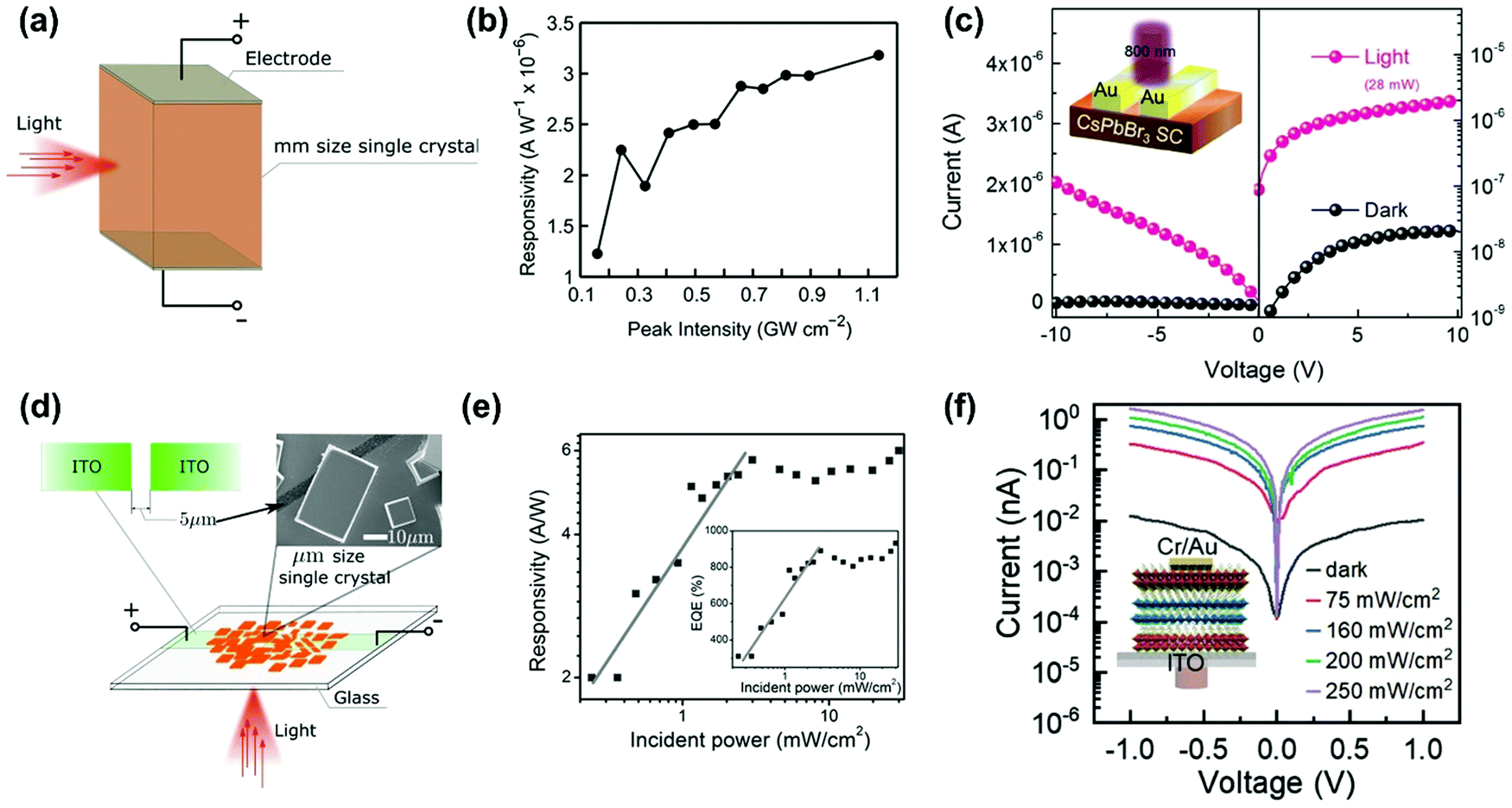 | ||
| Fig. 22 (a) Photodetector schemes based on a mm-size lead halide perovskite single crystal. (b) Excitation intensity dependent responsivity of a CH3NH3PbBr3 single crystal-based sub-bandgap photodetector. (c) I–V and I–V logarithm characteristics of a sub-bandgap photodetector in the dark and under 800 nm (28 mW) illumination. Inset: Schematic diagram of an IR photodetector device structure. (d) Photodetector scheme based on a μm-size lead halide perovskite single crystal. (e) Power-dependent responsivity (R) and EQE under V = 3 V bias and λex = 800 nm. (f) The I–V characteristics of the 2D perovskite heterostructure device with a thickness of 20 μm in the dark and under 980 nm laser irradiation with different powers. Inset is schematic of the photodetector based on the n = 1/n = 2 heterostructure. (b) Reprinted with permission from ref. 59. Copyright 2015 American Chemical Society. (c) Reprinted with permission from ref. 100. Copyright 2017 Wiley-VCH Verlag GmbH & Co. KGaA, Weinheim. (e) Reprinted with permission from ref. 89. Copyright 2017 Wiley-VCH Verlag GmbH & Co. KGaA, Weinheim. (f) Reprinted with permission from ref. 70. Copyright 2019 Wiley-VCH Verlag GmbH & Co. KGaA, Weinheim. | ||
The sub-bandgap photodetector discussed above uses the halide perovskite with a size of several millimeters to centimeter.100,162 The size is several orders of magnitudes larger than the diffusion length of charge carriers in halide perovskite materials (∼several μm). This can increase the possibility for the charge carriers to be trapped before they reach the electrodes. The performance (responsivity) of the devices might be diminished due to trapping or other processes in the large crystals. This might be one of the reasons for the low responsivity (in the of order 10−7 A W−1) of the above mentioned sub-bandgap TPA photodetector based on a MAPbBr3 single crystal of a mm-size.59 Moreover, the TPA process occurs mostly at the focus spot, which means that only a small portion of a large crystal is functioning as the active material for photodetection, and most of the crystal merely acts as a transport medium of charge carriers. This means that the large size crystals are not used in an efficient way. Furthermore, the long-distance charge carrier transportation will cause the slow response (both rise and decay times) of the photodetectors, which has been reported; the response time of CsPbBr3 single crystal based photodetectors is in few tens to hundreds ms under both TPA and OPA.167–173 In the work of Song et al.,100 they cut the cm size CsPbBr3 single crystal into 1.1 mm thick coins to fabricate the photodetector with a lateral configuration.171 In this way, they reduced the material consumption and decreased the transportation length of charge carriers. The responsivity of the device has reached 1.4 × 10⁻³ A W−1 for 800 nm light and a fast response has been shown (rise time: 111 μs, decay time: 575 μs).100
To overcome the low responsivity and slow response issues, we deposited lead halide perovskite microcrystals on a planar glass substrate with two ITO electrodes (with 5 μm channel width and 1000 μm length, see Fig. 22d).89 It has been reported that these crystalline films show mobility and diffusion length comparable with mm-size single crystals.164 Due to the fact that the size of the active material is comparable to the diffusion length, the charge carriers can be collected efficiently. Hence, the microcrystal layer-based photodetector devices show high performance. As shown in Fig. 22e, the responsivity of the photodetector increases with increasing input photon intensity and reaches the maximum 6 A W−1, the responsivity is about three orders of magnitude higher than that of the cm-size single crystal-based sub-bandgap photodetector.100 The corresponding external quantum efficiency (EQE) is over 800% (Fig. 22e). We utilized the configuration as illustrated in Fig. 22d to map the high-resolution photocurrent distribution161 by using the phase modulated two-photon excited photoluminescence/photocurrent method, which will be discussed in the section below.
As discussed in the sections above, two-dimensional perovskites show a large TPA coefficient. It is natural to use them as active materials for sub-bandgap photodetector applications. Wang et al. fabricated sub-bandgap photodetectors based on two-dimensional perovskite (n-C4H9NH3)2PbI4/(n-C4H9NH3)2(CH3NH3)Pb2I7 heterostructure (Fig. 22f). Taking the advantages of the high crystalline quality and low intrinsic carrier concentration of the heterostructures,70 the dark current is extremely low, in the order of 10−12 A. The photodetector also shows a fast response time (rise time: 124 ms, decay time: 110 ms), which is comparable to that of the photodetectors working in the linear OPA regime.70 They reached the responsivity to 10−7 A W−1 at an applied voltage of 1 V, which is about a 10-fold increase compared to their pure phase two-dimensional perovskite (n-C4H9NH3)2PbI4 or (n-C4H9NH3)2(CH3NH3)Pb2I7)) based photodetector. The enhanced responsivity is attributed to the large TPA coefficient of the heterostructure.70 Zhou et al. used two-dimensional (BA)2(MA)3Pb4I13 (BA = CH3CH2CH2CH2NH2, In=4) perovskites to fabricate a sub-bandgap photodetector (Fig. 23). Owing to the large TPA coefficient (640 cm GW−1), the photodetector shows two-photon current responsivity up to 1.2 × 104 cm2 W−2 s−1, which is two orders of magnitude greater than that of the standard InAsSbP-pin photodiode,114 and dark current as low as 2 × 10⁻¹² A at room temperature. Furthermore, the photodetectors is sensitive to light polarization of the incoming near infrared photons. Recently, Peng et al. developed chiral perovskite bulk crystal based sub-bandgap photodetectors, which show a responsivity of 3.5 × 10⁻⁶ A W−1 and low dark current of 2.5 pA.71 Due to the chiral properties of the crystal, the photodetectors have the potential for circularly polarized light sensitive direct detection.
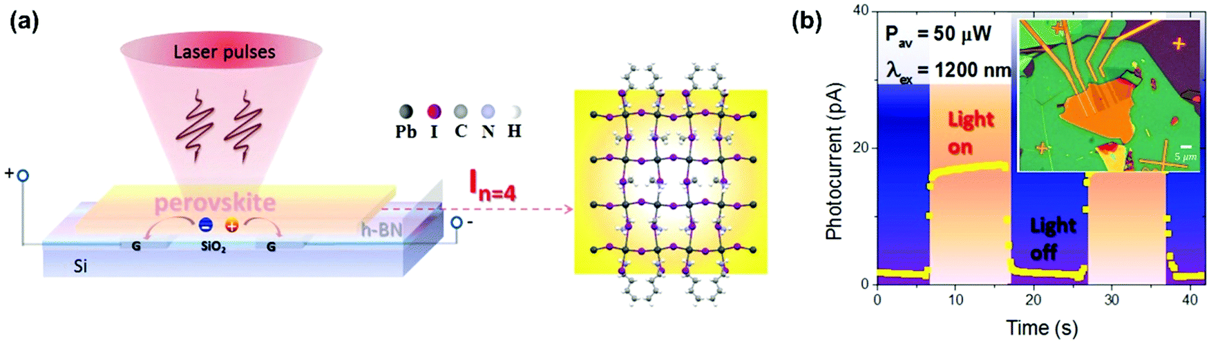 | ||
| Fig. 23 (a) Schematic representation of sub-bandgap photodetection based on 2D Ruddlesden–Popper halide perovskites (2D-RPPs). Right: a side view of the molecular structure for monolayer 2D-RPPs (from: In=4). (b) Photoswitching behavior under alternating ON and OFF laser pulses for the 2D-RPP (In=4) device, inset: optical images of the 2D-RPP (In=4 and In=2) device, respectively. Both In=4 and In=2 devices are encapsulated with few-layer h-BN (in green or in blue) for a highly stable performance. The circular region in white illustrates the laser spot; here a maximum signal in the photocurrent was observed (from: In=4). (a) and (b) Reprinted with permission from ref. 114. Copyright 2019 Wiley-VCH Verlag GmbH & Co. KGaA, Weinheim. | ||
6.3 Bioimaging
The excitation photon is in the near-infrared regime for TPA in halide perovskites. Near-infrared light has a longer penetration depth, weaker background and lower biological damage compared to visible light in bioimaging. Furthermore, owing to the nonlinear process, two-photon excited photoluminescence features high spatial resolution. Together with the large TPA cross-section and high photoluminescence quantum yield, halide perovskite nanomaterials show promising application for bioimaging.25 However, there are various obstacles for such application, such as low stability of lead halide perovskites,174 low water resistance, and the toxicity of lead. Different approaches have been developed to enhance the stability of lead halide perovskite nanomaterials.25,149,157,175–177Recently, Pramanik and co-workers used water to trigger an interfacial conversion from zero-dimensional Cs4PbBr5 nanocrystals to three-dimensional CsPbBr3 nanorods, nanoplatelets and nanocubes (Fig. 24a). Then they coated the transformed CsPbBr3 nanomaterials with amine–poly(ethylene glycol)–propionic acid ((NH2–PEG12–CH2–CH2–CO2H), PEG). The PEG can act as a protection layer to effectively prevent degradation, and increase the stability and biocompatibility of the perovskite nanomaterials. This approach is a widely used method for other types of nanoparticle encapsulation.178,179 The PEG coated CsPbBr3 nanomaterial shows high water-stability and photostability (both NIR and UV light), which retain 86% of photoluminescence intensity after 35 days in water (Fig. 24b); their photoluminescence intensity remains almost unchanged when they are placed under UV light for several hours (Fig. 24c). Furthermore, they found the PEG coated CsPbBr3 nanomaterials show excellent biocompatibility for different cancer cells and normal skin cells. Moreover, these PEG coated CsPbBr3 nanomaterials also show large TPA cross-section (Table 1). Motivated by these properties, they carried out two-photon excited cell-imaging experiment with these PEG-coated CsPbBr3 nanomaterials. They conjugated PEG coated CsPbBr3 nanoplatelets (blue color emission) with anti-AXL antibody to image TNBC cells with two-photon excited luminescence imaging (Fig. 24d). Similarly, they conjugated PEG coated CSPbBr3 nanorods (green color emission) with anti-HER-2 antibody to image HER-2(+) SK-BR-3 cells with two-photon excited luminescence imaging (Fig. 24e). They also determined that nanorods (with anti-AXL antibody) and nanoplatelets (anti-HER-2 antibody) can simultaneously image MDA-MB-231 TNBC cells and HER-2(+) SK-BR-3 cells with two-photon excitation (Fig. 24f), respectively. The promising results from this work will stimulate more research to focus on developing halide perovskite nanomaterials for two-photon bioimaging applications. At the moment, several approaches have been proposed to encapsulate halide perovskite materials in polymer, SiO2 and glass to increase their stability in water.25,149,157,175–177,180–182 With all the expectations we discussed above, we are in the right direction to use halide perovskite materials for bioimaging applications.
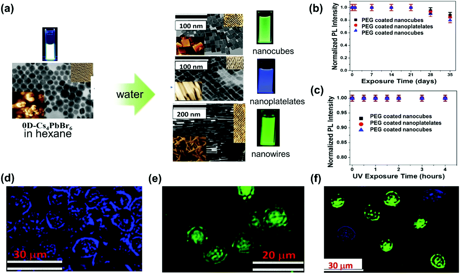 | ||
| Fig. 24 (a) TEM image, inserted high resolution TEM (HRTEM) image, inserted SEM image, and photograph of water resistant 1D, 2D, and 3D CsPbBr3 perovskite nanocrystals derived through an interfacial conversion from 0D Cs4PbBr6 nanocrystals using different amounts of water. (b) Change of normalized photoluminescence (PL) intensity (PL intensity at certain time/PL intensity initially) with time for PEG coated 1D, 2D, and 3D CsPbBr3 nanocrystals when they are kept under water. (c) PL intensity for PEG coated 1D, 2D, and 3D CsPbBr3 nanocrystals as a function of UV light exposure time. We used 360 nm UV-light with 30 mW cm−2 power. (d) Two-photon luminescence image from PR(−) ER(−) HER-2(−) MDA-MB-231 breast cancer cells which are attached to anti-AXL antibody conjugated 2D CsPbBr3 nanoplatelets. (e) Two-photon luminescence image from HER-2(+) SK-BR-3 breast cancer cells which are attached to anti-HER-2 antibody conjugated 1D CsPbBr3 nanowires. (f) Two-photon luminescence image from a mixture of PR(−) ER(−) HER-2(−) MDA-MB-231 breast cancer and HER-2(+) SK-BR-3 breast cancer cells. For multicolor imaging, we used anti-AXL antibody conjugated 2D CsPbBr3 nanoplatelets and anti-HER-2 antibody conjugated 1D CsPbBr3 nanowires together. (a)-(f) Reprinted with permission from ref. 25. Copyright the authors. | ||
6.4 Imaging spatial heterogeneity in halide perovskite with two-photon excitation
TPA in halide perovskite materials also offer the possibility to study their spatial heterogeneity by using two-photon excited microscopies. The spatial heterogeneity of carrier dynamics and trap-state distribution inside the perovskite crystals and films can be mapped by using two-photon excited transient absorption, photoluminescence and photocurrent microscopies,161,183–185 owing to the two-photon excitation showing long penetration depth and high spatial confinement to the focal point of the exciting beam. This can give a clear picture about how the spatial heterogeneity and trap-states affect the optoelectronic properties in the halide perovskite-based devices. A clarification about these fundamental issues can help further improving the performance of the perovskite-based optoelectronic devices.The halide perovskite thin films prepared by low-temperature process are widely used for fabricating photoelectronic devices, such as photovoltaics. However, there are often grains, fibers, grain boundaries or other spatial structures in the films.186 It has been reported that the spatial heterogeneity plays an important role in the performance of halide perovskite based devices.187 As shown in Fig. 25a and b, the one-photon and two-photon excited photoluminescence microscopy images have been taken in the same region by C. Stavrakas et al.185 Due to the different penetration depths, the one-photon excited photoluminescence is selectively generated on/near the surface; the two-photon excited photoluminescence is generated from the bulk of the film. Some grains (in red circles in Fig. 25a and b) appear to be brighter on the surface than in the bulk, while some grains (in green circles) show the opposite. The contrast between bright and dark grains is much higher in two-photon excitation than in one-photon excitation (Fig. 25c); this difference might be due to the charge carrier diffusion through grain boundary being more difficult in the bulk compared to at the surface. They imaged the two-photon excited photoluminescence intensity and lifetime in micro-sized single crystals (Fig. 25d–f). In some microcrystals (blue circles), strong photoluminescence intensity is associated with long lifetime, while in other microcrystals (green circles) do not show such correlation. Yu et al. combined two-photon excited fs-TA and photoluminescence microscopy to map the spatial heterogeneity of charge carrier dynamics in polycrystalline MAPbI3 films.183 From the two-photon excited transient absorption and photoluminescence mapping, one can observe that regions with short (at the ps time scale) negative transient absorption tend to have longer photoluminescence lifetimes. This correlation could indicate the presence of sub-band edge states, which have long photoluminescence lifetime.183,188 They found such spatial inhomogeneity of carrier dynamics is not directly correlated with the surface structure, indicating that composition heterogeneity is a critical factor for local charge carrier relaxation.183
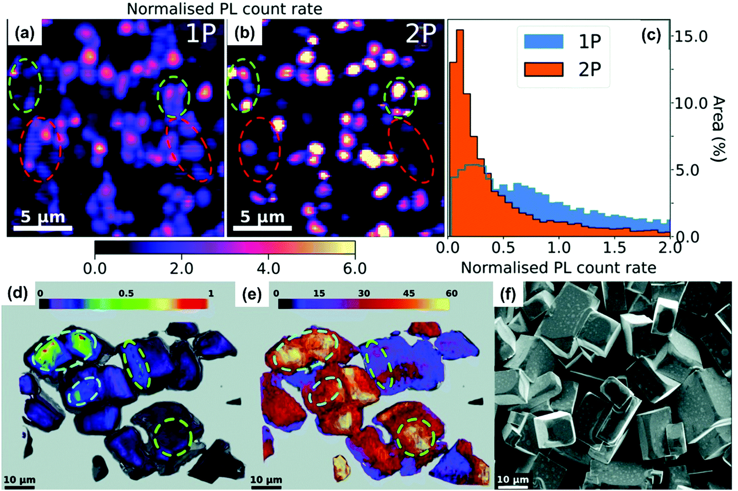 | ||
| Fig. 25 2D photoluminescence (PL) maps of a MAPbI3 film normalized to their respective mean using (a) one-photon (1P-PL) and (b) two-photon (2P-PL) excitation at 510 nm and 1100 nm respectively, with a pulsed (5 MHz, pulse width 150 fs) excitation density of ∼1016 cm−3. (c) Comparison of the PL distributions from the two maps, normalized by the mean of each. The red dotted circles in (a) and (b) highlight grain clusters that are bright at the surface and dark in the bulk; the green dotted circles show the opposite trend. (d) Total PL intensity and the (e) extracted lifetime, with both images showing some pockets of strong PL associated with long lifetime (blue circles) and some showing the opposite behavior (green circles). (f) Representative SEM image of the crystal films. (a)–(f) Reprinted with permission from ref. 185. Copyright the Royal Society of Chemistry 2018. | ||
We studied two-photon excited photocurrent in MAPbBr3 micro-sized crystals by using a new high-resolution photoluminescence and photocurrent microscopy, which was developed by combining TPA and phase modulation technique.161 This two-photon microscopy is a powerful technique to characterize charge carrier mobility and defects in semiconductor materials.161,189 We placed MAPbBr3 micro-sized crystals between two ITO electrodes (inset Fig. 26a) as shown in the scheme in Fig. 22d, where different bias can be applied.161 We mapped the two-photon excited photocurrent of the micro-sized crystals with different bias applied (Fig. 26a–c). We found that the charge carrier transport length in the microcrystals depends on the applied electric field, which can be increased from 5.7 μm (with 0.02 V bias) to 23.2 μm (with 2 V bias). Under a 0.02 V bias, photocurrent intensity distribution in the microcrystal is mainly located along the ITO gap (Fig. 26d). This is because the very low voltage bias only creates a small band bending near the electrode gap providing current flow only in that region, while the charge carriers far away from the gap perform random diffusive motion (Fig. 26e). In this case the spatial pattern of the photocurrent is mainly determined by the minority carrier diffusion length. With increasing bias, the photocurrent distribution becomes broader (Fig. 26b and c) along the X axis. This is because the applied bias (electric field) creates a larger band bending between the electrodes and the perovskite microcrystals, which accelerates the carrier transport. As the carrier drift becomes important at a higher bias, the spatial photocurrent profile is related to the hole drift length, which depends on the electric field. Furthermore, the photocurrent shows strong variations over the crystal (Fig. 26f). This is attributed to the distribution of trap states in the microcrystals.
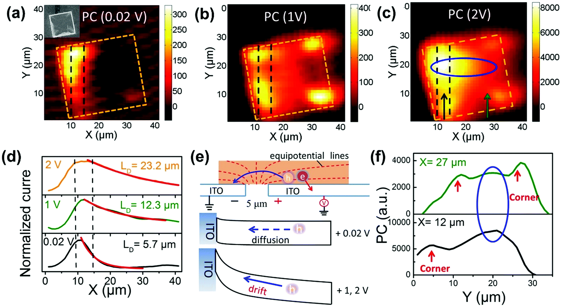 | ||
| Fig. 26 Photocurrent (PC) mapping with (a) 0.02, (b) 1, and (c) 2 V bias. The orange dashed line indicates the microcrystal edge, and the two black dashed lines show the ITO gap. Inset in (a): SEM image of the MAPbBr3 MC device used in the experiment. (d) Average PC decay length along the X axis with different voltage bias. (e) Illustration of electron and hole transfer (top) and hole diffusion (+0.02 V) and drift (+1, 2 V) in the valence band. (f) PC intensity along the Y axis at different X values with 2 V bias. (a)–(f) Reprinted with permission from ref. 161. Copyright 2018 American Chemical Society. | ||
6.5 Optical limiting
Optical limiting has attracted significant attention because of the increased demand for delicate optical sensors that can protect human body (especially eyes) from laser damage.24 It is reported that there are many kinds of materials that have the optical limiting properties, including organic dyes,190–192 semiconductor materials,193,194 organic polymers,195,196 and carbon nanostructured materials.197,198 Halide perovskite materials show optical limiting properties as well, as most of the intense laser power can be absorbed by halide perovskites once the laser beam power has reached the TPA threshold.27,199,200A good optical limiting material is required to have a low TPA threshold, a high TPA coefficient, a high thermal stability, and a large thickness, so that the transmittance with low intensity will be obtained.24 Halide perovskite materials have the potential to fulfil these requirements. Li et al. synthesized a series of all-inorganic perovskite quantum dots CsPbX3 (X = Cl, Br, or I) and SiO2@CsPbX3 that are coated with SiO2,201 and the optical limiting properties of these quantum dots were investigated by open-aperture Z-scan technique under excitation of a 532 nm laser beam. They found that SiO2@CsPbX3 quantum dots possess composition-dependent optical limiting properties (Fig. 27), in which the SiO2@CsPbBr3 exhibits the best optical limiting properties, whose optical limiting threshold is 1.68 J cm−2 (for nanosecond laser pulse). As the practical application of optical limiters is in the solid state form, it is preferred to fabricate solid state optical limiters based on halide perovskites. Jin et al. embedded the CsPbX3 nanocrystals into the SiO2–Al2O3–MgO–ZnO–B2O3 glass matrix.26 These CsPbX3 nanocrystal embedded glasses show high TPA coefficients (24.1 cm GW−1), high thermostability, light stability and water resistance, and all these are prerequisite for optical limiting application. It is also very important to actively explore the optical limiting applications of low-dimensional perovskites owing to their large TPA coefficient (Fig. 15b and Table 1). Recently, Zhao et al. fabricated a 2D Ruddelesden–Popper (RP) hybrid perovskite (CH3(CH2)3NH3)2(CH3NH3)n−1PbnI3n+1 (n = 1, 2, 3, 4) with an average size of 5–7 nm by applying the top-down synthesizing method.202 By using Z-scan technique, they revealed a TPA coefficient of up to 650 cm GW−1; besides, they found that the 2D perovskites feature >50% of the optical limiting at 80 μJ and a maximum of 86% of the optical limiting at 150 μJ, showing great potential in optical limiting applications.
 | ||
| Fig. 27 Optical limiting curves of the SiO2@CsPbX3 quantum dots at (a) nanosecond and (b) picosecond duration laser excitation. Points indicate experimental data and solid lines show the curves of best-fit. (a) and (b) Reprinted with permission from ref. 201. Copyright 2020 Published by Elsevier B.V. | ||
7. Conclusions and perspectives
Over the past several years, we have witnessed the vigorous development and explosive progress in the field of halide perovskite materials. Numerous investigations have been devoted to the synthetic methodology of new kinds of perovskites. Though the research in the TPA and its application in these materials are still relatively limited, the increasing number of studies has demonstrated plentiful promising opportunities for the realization of various technically important applications, such as up-conversion lasers, sub-bandgap photodetectors, imaging, and optical limiting. In this review, we have summarized the recent advances in the studies of TPA in halide perovskite materials. We have discussed details of the photophysical processes in two-photon excited halide perovskites and compared the explanations of the differences in photoluminescence after one- and two-photon excitation. Based on a detailed description of two-photon absorption, we have summarized the factors that affect the TPA properties and have discussed numerous potential applications of the TPA in this family of materials.While a lot has been understood, still many issues need clarification. From the materials science point of view, more research efforts are required to understand the charge carrier dynamics under TPA, investigating TPA properties of lead-free perovskites as they have decreased dimensionality, understanding how the quantum confinement influences TPA properties in halide perovskites and how the defects influence TPA.
It is a promising approach to use halide perovskite materials for sub-bandgap photodetection via TPA. However, the nonlinear nature of TPA requires the excitation intensity to be several orders of magnitude higher than the OPA process. This limits the application of TPA based sub-bandgap photodetection only for high power laser and, perhaps, for short-pulsed laser light detection. To overcome such limitation, we should seek for materials with a large TPA coefficient.
From the bioimaging point of view, developing non-toxic lead-free halide perovskite nanomaterials with large TPA cross-section and high photoluminescence quantum yield is necessary. Alternatively, one may encapsulate the lead halide perovskite nanomaterials in a shell of a biocompatible material.149,157
Since TPA is related to high excitation powers, long-term stability of halide perovskite materials under such conditions is an important challenge that needs to be further improved. Various 0D, 1D and 2D nanostructured halide perovskites have shown promise in that direction. All in all, we, the authors, foresee a brightly shining future for the TPA applications of halide perovskites.
Author contributions
J. C., W. Z. and T. P. conceptualized this project and all authors discussed, wrote, and commented on the manuscript.Conflicts of interest
There are no conflicts of interest to declare.Acknowledgements
This work was supported by the Lundbeckfonden (grant R303-2018-3237), the Swedish Research Council (VR) and Swedish Energy Agency.References
- G. S. He, L. S. Tan, Q. Zheng and P. N. Prasad, Chem. Rev., 2008, 108, 1245–1330 CrossRef CAS PubMed.
- K. Chen, S. Schünemann, S. Song and H. Tüysüz, Chem. Soc. Rev., 2018, 47, 7045–7077 RSC.
- V. M. Goldschmidt, Naturwissenschaften, 1926, 14, 477–485 CrossRef CAS.
- B. Saparov and D. B. Mitzi, Chem. Rev., 2016, 116, 4558–4596 CrossRef CAS PubMed.
- D. B. Mitzi, Prog. Inorg. Chem., 1999, 48, 1–121 CAS.
- G. Wang, S. Mei, J. Liao, W. Wang, Y. Tang, Q. Zhang, Z. Tang, B. Wu and G. Xing, Small, 2021, 17, 2100809 CrossRef CAS PubMed.
- E. I. Marchenko, S. A. Fateev, A. A. Petrov, V. V. Korolev, A. Mitrofanov, A. V. Petrov, E. A. Goodilin and A. B. Tarasov, Chem. Mater., 2020, 32, 7383–7388 CrossRef CAS.
- D. B. Mitzi, Chem. Mater., 1996, 8, 791–800 CrossRef CAS.
- L. Mao, W. Ke, L. Pedesseau, Y. Wu, C. Katan, J. Even, M. R. Wasielewski, C. C. Stoumpos and M. G. Kanatzidis, J. Am. Chem. Soc., 2018, 140, 3775–3783 CrossRef CAS PubMed.
- Z. Xiao, Z. Song and Y. Yan, Adv. Mater., 2019, 31, e1803792 CrossRef PubMed.
- F. Giustino and H. J. Snaith, ACS Energy Lett., 2016, 1, 1233–1240 CrossRef CAS.
- B. Yang, J. S. Chen, F. Hong, X. Mao, K. B. Zheng, S. Q. Yang, Y. J. Li, T. Pullerits, W. Q. Deng and K. L. Han, Angew. Chem., Int. Ed., 2017, 56, 12471–12475 CrossRef CAS PubMed.
- D. M. Jang, K. Park, D. H. Kim, J. Park, F. Shojaei, H. S. Kang, J.-P. Ahn, J. W. Lee and J. K. Song, Nano Lett., 2015, 15, 5191–5199 CrossRef CAS PubMed.
- A. B. Feng, X. M. Jiang, X. Y. Zhang, X. P. Zheng, W. T. Zheng, O. F. Mohammed, Z. L. Chen and O. M. Bakr, Chem. Mater., 2020, 32, 7602–7617 CrossRef CAS.
- X. Zhang, L. Li, Z. Sun and J. Luo, Chem. Soc. Rev., 2019, 48, 517–539 RSC.
- L. Chouhan, S. Ghimire, C. Subrahmanyam, T. Miyasaka and V. Biju, Chem. Soc. Rev., 2020, 49, 2869–2885 RSC.
- X. Han, Y. Zheng, S. Chai, S. Chen and J. Xu, Nanophotonics, 2020, 9, 1787–1810 CrossRef CAS.
- A. Ferrando, J. P. Martínez Pastor and I. Suárez, J. Phys. Chem. Lett., 2018, 9, 5612–5623 CrossRef CAS PubMed.
- Y. Zhou, Y. Huang, X. Xu, Z. Fan, J. B. Khurgin and Q. Xiong, Appl. Phys. Rev., 2020, 7, 041313 CAS.
- F. Zhou, X. Ran, D. Fan, S. Lu and W. Ji, Adv. Opt. Mater., 2021, 9, 2100292 CrossRef CAS.
- J. K. Zaręba, M. Nyk and M. Samoć, Adv. Opt. Mater., 2021, 9, 2100216 CrossRef.
- J. Xu, X. Li, J. Xiong, C. Yuan, S. Semin, T. Rasing and X.-H. Bu, Adv. Mater., 2020, 32, 1806736 CrossRef CAS PubMed.
- W. Chen, F. Zhang, C. Wang, M. Jia, X. Zhao, Z. Liu, Y. Ge, Y. Zhang and H. Zhang, Adv. Mater., 2021, 33, 2004446 CrossRef CAS PubMed.
- W. Shen, J. Chen, J. Wu, X. Li and H. Zeng, ACS Photonics, 2021, 8, 113–124 CrossRef CAS.
- A. Pramanik, S. Patibandla, Y. Gao, K. Gates and P. C. Ray, JACS Au, 2021, 1, 53–65 CrossRef CAS PubMed.
- M. Jin, X. Liang, H. Zhang, J. Liu, G. Shao, W. Xiang and Y. Song, J. Eur. Ceram. Soc., 2020, 40, 4140–4147 CrossRef CAS.
- K. S. Rao, R. A. Ganeev, K. Zhang, Y. Fu, G. S. Boltaev, S. K. Maurya and C. Guo, Opt. Mater., 2019, 92, 366–372 CrossRef CAS.
- M. Pawlicki, H. A. Collins, R. G. Denning and H. L. Anderson, Angew. Chem., Int. Ed., 2009, 48, 3244–3266 CrossRef CAS PubMed.
- M. Rumi and J. W. Perry, Adv. Opt. Photonics, 2010, 2, 451–518 CrossRef CAS.
- J. Olesiak-Banska, M. Waszkielewicz, P. Obstarczyk and M. Samoc, Chem. Soc. Rev., 2019, 48, 4087–4117 RSC.
- M. Göppert-Mayer, Ann. Phys., 1931, 401, 273–294 CrossRef.
- W. Kaiser and C. G. B. Garrett, Phys. Rev. Lett., 1961, 7, 229–231 CrossRef CAS.
- M. Drobizhev, N. S. Makarov, S. E. Tillo, T. E. Hughes and A. Rebane, Nat. Methods, 2011, 8, 393–399 CrossRef CAS PubMed.
- R. Scott, A. W. Achtstein, A. Prudnikau, A. Antanovich, S. Christodoulou, I. Moreels, M. Artemyev and U. Woggon, Nano Lett., 2015, 15, 4985–4992 CrossRef CAS PubMed.
- W. L. Peticolas, Annu. Rev. Phys. Chem., 1967, 18, 233–260 CrossRef CAS.
- W. M. McClain, Acc. Chem. Res., 1974, 7, 129–135 CrossRef CAS.
- C. Xu and W. W. Webb, in Topics in Fluorescence Spectroscopy: Volume 5: Nonlinear and Two-Photon-Induced Fluorescence, ed. J. R. Lakowicz, Springer US, Boston, MA, 2002 Search PubMed.
- Y. R. Shen, The Principles of Nonlinear Optics, Wiley-Interscience, New York, 1984 Search PubMed.
- R. W. Boyd, in Nonlinear Optics, ed. R. W. Boyd, Academic Press, Burlington, 3rd edn, 2008 Search PubMed.
- R. L. Sutherland, Handbook of Nonlinear Optics, Marcel Dekker, Inc., New York, 2nd edn, 2003 Search PubMed.
- J. R. Lakowicz, Principles of fluorescence spectroscopy, Springer Science & Business Media, 2013 Search PubMed.
- A. Einstein, B. Podolsky and N. Rosen, Phys. Rev., 1935, 47, 777–780 CrossRef CAS.
- J. Javanainen and P. L. Gould, Phys. Rev. A: At., Mol., Opt. Phys., 1990, 41, 5088–5091 CrossRef CAS PubMed.
- S. Friberg, C. K. Hong and L. Mandel, Opt. Commun., 1985, 54, 311–316 CrossRef.
- J. Gea-Banacloche, Phys. Rev. Lett., 1989, 62, 1603–1606 CrossRef CAS PubMed.
- Z. Y. Ou, C. K. Hong and L. Mandel, J. Opt. Soc. Am. B, 1987, 4, 1574–1587 CrossRef CAS.
- D.-I. Lee and T. Goodson, J. Phys. Chem. B, 2006, 110, 25582–25585 CrossRef CAS PubMed.
- N. P. Georgiades, E. S. Polzik, K. Edamatsu, H. J. Kimble and A. S. Parkins, Phys. Rev. Lett., 1995, 75, 3426–3429 CrossRef CAS PubMed.
- B. Dayan, A. Pe’er, A. A. Friesem and Y. Silberberg, Phys. Rev. Lett., 2005, 94, 043602 CrossRef PubMed.
- L. Upton, M. Harpham, O. Suzer, M. Richter, S. Mukamel and T. Goodson III, J. Phys. Chem. Lett., 2013, 4, 2046–2052 CrossRef CAS PubMed.
- A. R. Guzman, M. R. Harpham, O. z n Süzer, M. M. Haley and T. G. Goodson III, J. Am. Chem. Soc., 2010, 132, 7840–7841 CrossRef CAS PubMed.
- M. R. Harpham, O. z n Süzer, C.-Q. Ma, P. Bäuerle and T. Goodson III, J. Am. Chem. Soc., 2009, 131, 973–979 CrossRef CAS PubMed.
- B. Dayan, A. Pe'er, A. A. Friesem and Y. Silberberg, Phys. Rev. Lett., 2004, 93, 023005 CrossRef PubMed.
- J. P. Villabona-Monsalve, R. K. Burdick and T. Goodson, J. Phys. Chem. C, 2020, 124, 24526–24532 CrossRef CAS.
- K. M. Parzuchowski, A. Mikhaylov, M. D. Mazurek, R. N. Wilson, D. J. Lum, T. Gerrits, C. H. Camp, M. J. Stevens and R. Jimenez, Phys. Rev. Appl., 2021, 15, 044012 CrossRef CAS.
- T. Landes, M. Allgaier, S. Merkouche, B. J. Smith, A. H. Marcus and M. G. Raymer, Phys. Rev. Res., 2021, 3, 033154 CrossRef CAS.
- M. Sheik-Bahae, A. A. Said, T. Wei, D. J. Hagan and E. W. V. Stryland, IEEE J. Quantum Electron., 1990, 26, 760–769 CrossRef CAS.
- V. Singh and P. Aghamkar, AIP Conf. Proc., 2015, 1675, 030095 CrossRef.
- G. Walters, B. R. Sutherland, S. Hoogland, D. Shi, R. Comin, D. P. Sellan, O. M. Bakr and E. H. Sargent, ACS Nano, 2015, 9, 9340–9346 CrossRef CAS PubMed.
- R. de Nalda, R. del Coso, J. Requejo-Isidro, J. Olivares, A. Suarez-Garcia, J. Solis and C. N. Afonso, J. Opt. Soc. Am. B, 2002, 19, 289–296 CrossRef CAS.
- L. Yang, K. Wei, Z. Xu, F. Li, R. Chen, X. Zheng, X. Cheng and T. Jiang, Opt. Lett., 2018, 43, 122–125 CrossRef CAS PubMed.
- Z. Liu, Z. Hu, Z. Zhang, J. Du, J. Yang, X. Tang, W. Liu and Y. Leng, ACS Photonics, 2019, 6, 3150–3158 CrossRef CAS.
- Y. Wang, X. Li, X. Zhao, L. Xiao, H. Zeng and H. Sun, Nano Lett., 2016, 16, 448–453 CrossRef CAS PubMed.
- L. Zhou, Y. Tan, J. Wang, W. Xu, Y. Yuan, W. Cai, S. Zhu and J. Zhu, Nat. Photonics, 2016, 10, 393–398 CrossRef CAS.
- Q. Han, W. Wu, W. Liu, Q. Yang and Y. Yang, Opt. Mater., 2018, 75, 880–886 CrossRef CAS.
- V. Krivenkov, P. Samokhvalov, D. Dyagileva, A. Karaulov and I. Nabiev, ACS Photonics, 2020, 7, 831–836 CrossRef CAS.
- Y. Xu, Q. Chen, C. Zhang, R. Wang, H. Wu, X. Zhang, G. Xing, W. W. Yu, X. Wang, Y. Zhang and M. Xiao, J. Am. Chem. Soc., 2016, 138, 3761–3768 CrossRef CAS PubMed.
- W.-G. Lu, C. Chen, D. Han, L. Yao, J. Han, H. Zhong and Y. Wang, Adv. Opt. Mater., 2016, 4, 1732–1737 CrossRef CAS.
- W. Liu, J. Xing, J. Zhao, X. Wen, K. Wang, P. Lu and Q. Xiong, Adv. Opt. Mater., 2017, 5, 1601045 CrossRef.
- J. Wang, Y. Mi, X. Gao, J. Li, J. Li, S. Lan, C. Fang, H. Shen, X. Wen, R. Chen, X. Liu, T. He and D. Li, Adv. Opt. Mater., 2019, 7, 1900398 CrossRef.
- Y. Peng, X. Liu, L. Li, Y. Yao, H. Ye, X. Shang, X. Chen and J. Luo, J. Am. Chem. Soc., 2021, 143, 14077–14082 CrossRef CAS PubMed.
- C. Xu and W. W. Webb, J. Opt. Soc. Am. B, 1996, 13, 481–491 CrossRef CAS.
- D. A. Oulianov, I. V. Tomov, A. S. Dvornikov and P. M. Rentzepis, Opt. Commun., 2001, 191, 235–243 CrossRef CAS.
- Q. Han, W. Wu, W. Liu and Y. Yang, RSC Adv., 2017, 7, 35757–35764 RSC.
- Z. Cao, B. Lv, H. Zhang, Y. Lv, C. Zhang, Y. Zhou, X. Wang and M. Xiao, J. Chem. Phys., 2019, 151, 154201 CrossRef PubMed.
- G. L. Dakovski and J. Shan, J. Appl. Phys., 2013, 114, 014301 CrossRef.
- J. Chen, K. Žídek, P. Chábera, D. Liu, P. Cheng, L. Nuuttila, M. J. Al-Marri, H. Lehtivuori, M. E. Messing, K. Han, K. Zheng and T. Pullerits, J. Phys. Chem. Lett., 2017, 8, 2316–2321 CrossRef CAS PubMed.
- J. Chen, P. Chábera, T. Pascher, M. E. Messing, R. Schaller, S. Canton, K. Zheng and T. Pullerits, J. Phys. Chem. Lett., 2017, 8, 5119–5124 CrossRef CAS PubMed.
- F. O. Saouma, C. C. Stoumpos, M. G. Kanatzidis, Y. S. Kim and J. I. Jang, J. Phys. Chem. Lett., 2017, 8, 4912–4917 CrossRef CAS PubMed.
- J. Zhang, T. Jiang, X. Zheng, C. Shen and X. A. Cheng, Opt. Lett., 2017, 42, 3371–3374 CrossRef CAS PubMed.
- W. Ge, J. Shi, M. Xu, Y. Wu, H. Sugimoto and M. Fujii, Opt. Mater., 2021, 113, 110822 CrossRef CAS.
- J. Z. Li, S. F. Zhang, H. X. Dong, X. Q. Yuan, X. W. Jiang, J. Wang and L. Zhang, CrystEngComm, 2016, 18, 7945–7949 RSC.
- W. Chen, S. Bhaumik, S. A. Veldhuis, G. Xing, Q. Xu, M. Grätzel, S. Mhaisalkar, N. Mathews and T. C. Sum, Nat. Commun., 2017, 8, 15198 CrossRef CAS PubMed.
- J. H. Lin, L. Gomez, C. de Weerd, Y. Fujiwara, T. Gregorkiewicz and K. Suenaga, Nano Lett., 2016, 16, 7198–7202 CrossRef CAS PubMed.
- M. Brennan, J. Herr, T. Nguyen-Beck, J. Zinna, S. Draguta, S. Rouvimov, J. Parkhill and M. Kuno, J. Am. Chem. Soc., 2017, 139, 12201–12208 CrossRef CAS PubMed.
- B. Wu, H. T. Nguyen, Z. Ku, G. Han, D. Giovanni, N. Mathews, H. J. Fan and T. C. Sum, Adv. Energy Mater., 2016, 6, 1600551 CrossRef.
- O. Schuster, P. Wientjes, S. Shrestha, I. Levchuk, M. Sytnyk, G. J. Matt, A. Osvet, M. Batentschuk, W. Heiss, C. J. Brabec, T. Fauster and D. Niesner, Nano Lett., 2020, 20, 3090–3097 CrossRef CAS PubMed.
- Y. D. Glinka, R. Cai, X. Gao, D. Wu, R. Chen and X. W. Sun, AIP Adv., 2020, 10, 065028 CrossRef CAS.
- B. Yang, F. Zhang, J. Chen, S. Yang, X. Xia, T. Pullerits, W. Deng and K. Han, Adv. Mater., 2017, 29, 1703758 CrossRef PubMed.
- M. Sebastian, J. A. Peters, C. C. Stoumpos, J. Im, S. S. Kostina, Z. Liu, M. G. Kanatzidis, A. J. Freeman and B. W. Wessels, Phys. Rev. B, 2015, 92, 235210 CrossRef.
- Q. Wang and W. Wu, Opt. Lett., 2018, 43, 4923–4926 CrossRef CAS PubMed.
- T. Yamada, Y. Yamada, H. Nishimura, Y. Nakaike, A. Wakamiya, Y. Murata and Y. Kanemitsu, Adv. Electron. Mater., 2016, 2, 1500290 CrossRef.
- Y. Yamada, T. Yamada, Q. Phuong le, N. Maruyama, H. Nishimura, A. Wakamiya, Y. Murata and Y. Kanemitsu, J. Am. Chem. Soc., 2015, 137, 10456–10459 CrossRef CAS PubMed.
- K. Schotz, A. M. Askar, W. Peng, D. Seeberger, T. P. Gujar, M. Thelakkat, A. Kohler, S. Huettner, O. M. Bakr, K. Shankar and F. Panzer, J. Mater. Chem. C, 2020, 8, 2289–2300 RSC.
- T. Yamada, Y. Yamada, Y. Nakaike, A. Wakamiya and Y. Kanemitsu, Phys. Rev. Appl., 2017, 7, 014001 CrossRef.
- T. Yamada, T. Aharen and Y. Kanemitsu, Phys. Rev. Lett., 2018, 120, 057404 CrossRef CAS PubMed.
- Y. Fang, H. Wei, Q. Dong and J. Huang, Nat. Commun., 2017, 8, 14417 CrossRef CAS PubMed.
- M. Sheikbahae, D. J. Hagan and E. W. Vanstryland, Phys. Rev. Lett., 1990, 65, 96–99 CrossRef CAS PubMed.
- D. Yang, S. Chu, Y. Wang, C. K. Siu, S. Pan and S. F. Yu, Opt. Lett., 2018, 43, 2066–2069 CrossRef CAS PubMed.
- J. Song, Q. Cui, J. Li, J. Xu, Y. Wang, L. Xu, J. Xue, Y. Dong, T. Tian, H. Sun and H. Zeng, Adv. Opt. Mater., 2017, 5, 1700157 CrossRef.
- K. Ohara, T. Yamada, H. Tahara, T. Aharen, H. Hirori, H. Suzuura and Y. Kanemitsu, Phys. Rev. Mater., 2019, 3, 111601 CrossRef CAS.
- C. Kriso, M. Stein, T. Haeger, N. Pourdavoud, M. Gerhard, A. Rahimi-Iman, T. Riedl and M. Koch, Opt. Lett., 2020, 45, 2431–2434 CrossRef CAS PubMed.
- T.-C. Wei, S. Mokkapati, T.-Y. Li, C.-H. Lin, G.-R. Lin, C. Jagadish and J.-H. He, Adv. Funct. Mater., 2018, 28, 1707175 CrossRef.
- D. Yang, C. Xie, J. Sun, H. Zhu, X. Xu, P. You, S. P. Lau, F. Yan and S. F. Yu, Adv. Opt. Mater., 2016, 4, 1053–1059 CrossRef CAS.
- F. O. Saouma, D. Y. Park, S. H. Kim, M. S. Jeong and J. I. Jang, Chem. Mater., 2017, 29, 6876–6882 CrossRef CAS.
- A. Pramanik, K. Gates, Y. Gao, S. Begum and P. Chandra Ray, J. Phys. Chem. C, 2019, 123, 5150–5156 CrossRef CAS.
- J. Szeremeta, M. A. Antoniak, D. Wawrzyńczyk, M. Nyk and M. Samoć, Nanomaterials, 2020, 10, 1054 CrossRef CAS PubMed.
- I. Suárez, M. Vallés-Pelarda, A. F. Gualdrón-Reyes, I. Mora-Seró, A. Ferrando, H. Michinel, J. R. Salgueiro and J. P. M. Pastor, APL Mater., 2019, 7, 041106 CrossRef.
- J. Li, C. Ren, X. Qiu, X. Lin, R. Chen, C. Yin and T. He, Photonics Res., 2018, 6, 554 CrossRef CAS.
- R. A. Ganeev, K. S. Rao, Z. Yu, W. Yu, C. Yao, Y. Fu, K. Zhang and C. Guo, Opt. Mater. Express, 2018, 8, 1472–1483 CrossRef CAS.
- W.-Y. Liang, F. Liu, Y.-J. Lu, J. Popović, A. Djurišić and H. Ahn, Opt. Express, 2020, 28, 24919–24927 CrossRef CAS PubMed.
- L. Li, X. Shang, S. Wang, N. Dong, C. Ji, X. Chen, S. Zhao, J. Wang, Z. Sun, M. Hong and J. Luo, J. Am. Chem. Soc., 2018, 140, 6806–6809 CrossRef CAS PubMed.
- Q. Wei, B. Du, B. Wu, J. Guo, M. j Li, J. Fu, Z. Zhang, J. Yu, T. Hou, G. Xing, T. C. Sum and W. Huang, Adv. Opt. Mater., 2017, 5, 1700809 CrossRef.
- F. Zhou, I. Abdelwahab, K. Leng, K. P. Loh and W. Ji, Adv. Mater., 2019, 31, 1904155 CrossRef CAS PubMed.
- M. Li, Y. Xu, S. Han, J. Xu, Z. Xie, Y. Liu, Z. Xu, M. Hong, J. Luo and Z. Sun, Adv. Mater., 2020, 32, 2002972 CrossRef CAS PubMed.
- T. Takagahara and E. Hanamura, Phys. Rev. Lett., 1986, 56, 2533–2536 CrossRef CAS PubMed.
- T. He, J. Li, C. Ren, S. Xiao, Y. Li, R. Chen and X. Lin, Appl. Phys. Lett., 2017, 111, 211105 CrossRef.
- Y. Xie, J. Fan, C. Liu, S. Chi, Z. Wang, H. Yu, H. Zhang, Y. Mai and J. Wang, Adv. Opt. Mater., 2018, 6, 1700819 CrossRef.
- R. Subha, V. Nalla, J. H. Yu, S. W. Jun, K. Shin, T. Hyeon, C. Vijayan and W. Ji, J. Phys. Chem. C, 2013, 117, 20905–20911 CrossRef CAS.
- T. C. He, J. Z. Li, X. Qiu, S. Y. Xiao and X. D. Lin, Photonics Res., 2018, 6, 1021–1027 CrossRef CAS.
- F. Zhao, J. Li, J. Yu, Z. Guo, S. Xiao, Y. Gao, R. Pan, T. He and R. Chen, J. Phys. Chem. C, 2020, 124, 27169–27175 CrossRef CAS.
- S. Y. Zou, G. L. Yang, T. S. Yang, D. Zhao, Z. X. Gan, W. J. Chen, H. Z. Zhong, X. M. Wen, B. H. Jia and B. S. Zou, J. Phys. Chem. Lett., 2018, 9, 4878–4885 CrossRef CAS PubMed.
- R. Ketavath, N. K. Katturi, S. G. Ghugal, H. K. Kolli, T. Swetha, V. R. Soma and B. Murali, J. Phys. Chem. Lett., 2019, 10, 5577–5584 CrossRef CAS PubMed.
- B. Yang, J. Chen, S. Yang, F. Hong, L. Sun, P. Han, T. Pullerits, W. Deng and K. Han, Angew. Chem., Int. Ed., 2018, 57, 5359–5363 CrossRef CAS PubMed.
- L. Zhou, J.-F. Liao, Z.-G. Huang, J.-H. Wei, X.-D. Wang, H.-Y. Chen and D.-B. Kuang, Angew. Chem., Int. Ed., 2019, 58, 15435–15440 CrossRef CAS PubMed.
- J. B. Li, J. L. Duan, X. Y. Yang, Y. Y. Duan, P. Z. Yang and Q. W. Tang, Nano Energy, 2021, 80, 105526 CrossRef CAS.
- B. Yang and K. Han, Acc. Chem. Res., 2019, 52, 3188–3198 CrossRef CAS PubMed.
- W. Ke and M. G. Kanatzidis, Nat. Commun., 2019, 10, 965 CrossRef PubMed.
- T. He, J. Li, X. Qiu, S. Xiao, C. Yin and X. Lin, Adv. Opt. Mater., 2018, 6, 1800843 CrossRef.
- W. Chen, S. Zhang, M. Zhou, T. Zhao, X. Qin, X. Liu, M. Liu and P. Duan, J. Phys. Chem. Lett., 2019, 10, 3290–3295 CrossRef CAS PubMed.
- K. N. Krishnakanth, S. Seth, A. Samanta and S. V. Rao, Opt. Lett., 2018, 43, 603–606 CrossRef CAS PubMed.
- J. Li, Q. Jing, S. Xiao, Y. Gao, Y. Wang, W. Zhang, X. W. Sun, K. Wang and T. He, J. Phys. Chem. Lett., 2020, 11, 4817–4825 CrossRef CAS PubMed.
- G. Nagamine, J. O. Rocha, L. G. Bonato, A. F. Nogueira, Z. Zaharieva, A. A. R. Watt, C. H. de Brito Cruz and L. A. Padilha, J. Phys. Chem. Lett., 2018, 9, 3478–3484 CrossRef CAS PubMed.
- L. Protesescu, S. Yakunin, M. I. Bodnarchuk, F. Krieg, R. Caputo, C. H. Hendon, R. X. Yang, A. Walsh and M. V. Kovalenko, Nano Lett., 2015, 15, 3692–3696 CrossRef CAS PubMed.
- F. Zhao, J. Li, X. Gao, X. Qiu, X. Lin, T. He and R. Chen, J. Phys. Chem. C, 2019, 123, 9538–9543 CrossRef CAS.
- F. Zhang, C. Chen, S. V. Kershaw, C. Xiao, J. Han, B. Zou, X. Wu, S. Chang, Y. Dong, A. L. Rogach and H. Zhong, ChemNanoMat, 2017, 3, 303–310 CrossRef CAS.
- Q. Jing, Y. Su, X. Xing and Z. Lu, J. Mater. Chem. C, 2019, 7, 1854–1858 RSC.
- J. Ding, Y. Zhao, S. Du, Y. Sun, H. Cui, X. Zhan, X. Cheng and L. Jing, J. Mater. Sci., 2017, 52, 7907–7916 CrossRef CAS.
- L. Lv, Y. Xu, H. Fang, W. Luo, F. Xu, L. Liu, B. Wang, X. Zhang, D. Yang, W. Hu and A. Dong, Nanoscale, 2016, 8, 13589–13596 RSC.
- W. Peng, L. Wang, B. Murali, K.-T. Ho, A. Bera, N. Cho, C.-F. Kang, V. M. Burlakov, J. Pan, L. Sinatra, C. Ma, W. Xu, D. Shi, E. Alarousu, A. Goriely, J.-H. He, O. F. Mohammed, T. Wu and O. M. Bakr, Adv. Mater., 2016, 28, 3383–3390 CrossRef CAS PubMed.
- C. Xie, P. You, Z. Liu, L. Li and F. Yan, Light: Sci. Appl., 2017, 6, e17023 CrossRef PubMed.
- C. M. Sutter-Fella, D. W. Miller, Q. P. Ngo, E. T. Roe, F. M. Toma, I. D. Sharp, M. C. Lonergan and A. Javey, ACS Energy Lett., 2017, 2, 709–715 CrossRef CAS.
- B. H. Woo, I. C. Seo, J. Heo, Y. J. Yoon, J. Y. Kim and Y. C. Jun, Opt. Express, 2019, 27, 25293–25304 CrossRef CAS PubMed.
- Y. Pan, H. Wang, X. Li, X. Zhang, F. Liu, M. Peng, Z. Shi, C. Li, H. Zhang, Z. Weng, M. Gusain, H. Long, D. Li, J. Wang, Y. Zhan and L. Zheng, J. Mater. Chem. C, 2020, 8, 3359–3366 RSC.
- M. Pratheek, T. Abhinav, S. Bhattacharya, G. K. Chandra and P. Predeep, Mater. Sci. Energy Technol., 2021, 4, 282–289 CAS.
- Y. He, R. Su, Y. Huang, Y. Zhou, Q. Zhao, J. B. Khurgin, Q. Xiong and X. Xu, Adv. Funct. Mater., 2019, 29, 1904694 CrossRef.
- P. Li, Y. Chen, T. Yang, Z. Wang, H. Lin, Y. Xu, L. Li, H. Mu, B. N. Shivananju, Y. Zhang, Q. Zhang, A. Pan, S. Li, D. Tang, B. Jia, H. Zhang and Q. Bao, ACS Appl. Mater. Interfaces, 2017, 9, 12759–12765 CrossRef CAS PubMed.
- Y. Fan, P. Tonkaev, Y. Wang, Q. Song, J. Han, S. V. Makarov, Y. Kivshar and S. Xiao, Nano Lett., 2021, 21, 7191–7197 CrossRef CAS PubMed.
- R. Li, Z. Wei, H. Zhao, H. Yu, X. Fang, D. Fang, J. Li, T. He, R. Chen and X. Wang, Nanoscale, 2018, 10, 22766–22774 RSC.
- C. Becker, S. Burger, C. Barth, P. Manley, K. Jäger, D. Eisenhauer, G. Köppel, P. Chabera, J. Chen, K. Zheng and T. Pullerits, ACS Photonics, 2018, 5, 4668–4676 CrossRef CAS.
- W. Liu, X. Li, Y. Song, C. Zhang, X. Han, H. Long, B. Wang, K. Wang and P. Lu, Adv. Funct. Mater., 2018, 28, 1707550 CrossRef.
- S. Yuan, Y. Sheng, C. Liu, L. Yu, L. Dong, F. Xing, J. Zhang, Y. Di and Z. Gan, Appl. Phys. Lett., 2021, 119, 033302 CrossRef CAS.
- C. Cai, X. Wang, L. Ling, G. Bi, Z. Xu and H. Wu, Opt. Lett., 2019, 44, 658–661 CrossRef CAS PubMed.
- J. Chen, K. Zidek, M. Abdellah, M. J. Al-Marri, K. B. Zheng and T. Pullerits, J. Phys.: Condens. Matter, 2016, 28, 254001 CrossRef PubMed.
- R. Scheps, Prog. Quantum Electron., 1996, 20, 271–358 CrossRef CAS.
- H. Dong, C. Zhang, X. Liu, J. Yao and Y. S. Zhao, Chem. Soc. Rev., 2020, 49, 951–982 RSC.
- S. Li, D. Lei, W. Ren, X. Guo, S. Wu, Y. Zhu, A. L. Rogach, M. Chhowalla and A. K. Y. Jen, Nat. Commun., 2020, 11, 1192 CrossRef CAS PubMed.
- J. Pan, S. P. Sarmah, B. Murali, I. Dursun, W. Peng, M. R. Parida, J. Liu, L. Sinatra, N. Alyami, C. Zhao, E. Alarousu, T. K. Ng, B. S. Ooi, O. M. Bakr and O. F. Mohammed, J. Phys. Chem. Lett., 2015, 6, 5027–5033 CrossRef CAS PubMed.
- Z. Gu, K. Wang, W. Sun, J. Li, S. Liu, Q. Song and S. Xiao, Adv. Opt. Mater., 2016, 4, 472–479 CrossRef CAS.
- M. Csele, Fundamentals of Light Sources and Lasers, John Wiley & Sons, Inc., New Jersey, 2004 Search PubMed.
- B. Yang, J. Chen, Q. Shi, Z. Wang, M. Gerhard, A. Dobrovolsky, I. G. Scheblykin, K. J. Karki, K. Han and T. Pullerits, J. Phys. Chem. Lett., 2018, 9, 5017–5022 CrossRef CAS PubMed.
- Q. Q. Lin, A. Armin, P. L. Burn and P. Meredith, Laser Photonics Rev., 2016, 10, 1047–1053 CrossRef CAS.
- X. Hu, X. Zhang, L. Liang, J. Bao, S. Li, W. Yang and Y. Xie, Adv. Funct. Mater., 2014, 24, 7373–7380 CrossRef CAS.
- M. I. Saidaminov, V. Adinolfi, R. Comin, A. L. Abdelhady, W. Peng, I. Dursun, M. Yuan, S. Hoogland, E. H. Sargent and O. M. Bakr, Nat. Commun., 2015, 6, 9724 Search PubMed.
- V. Adinolfi, O. Ouellette, M. I. Saidaminov, G. Walters, A. L. Abdelhady, O. M. Bakr and E. H. Sargent, Adv. Mater., 2016, 28, 7264 CrossRef CAS PubMed.
- J. Ding and Q. F. Yan, Sci. China Mater., 2017, 60, 1063–1078 CrossRef CAS.
- J. Ding, S. Du, Z. Zuo, Y. Zhao, H. Cui and X. Zhan, J. Phys. Chem. C, 2017, 121, 4917–4923 CrossRef CAS.
- J.-H. Cha, J. H. Han, W. Yin, C. Park, Y. Park, T. K. Ahn, J. H. Cho and D.-Y. Jung, J. Phys. Chem. Lett., 2017, 8, 565–570 CrossRef CAS PubMed.
- M. I. Saidaminov, M. A. Haque, J. Almutlaq, S. Sarmah, X.-H. Miao, R. Begum, A. A. Zhumekenov, I. Dursun, N. Cho, B. Murali, O. F. Mohammed, T. Wu and O. M. Bakr, Adv. Opt. Mater., 2017, 5, 1600704 CrossRef.
- Q. Lin, A. Armin, P. L. Burn and P. Meredith, Laser Photonics Rev., 2016, 10, 1047–1053 CrossRef CAS.
- D. Hao, J. Zou and J. Huang, InfoMat, 2020, 2, 139–169 CrossRef CAS.
- J. Deng, J. Li, Z. Yang and M. Wang, J. Mater. Chem. C, 2019, 7, 12415–12440 RSC.
- J. Miao and F. Zhang, J. Mater. Chem. C, 2019, 7, 1741–1791 RSC.
- J. S. Chen, D. Z. Liu, M. J. Al-Marri, L. Nuuttila, H. Lehtivuori and K. B. Zheng, Sci. China Mater., 2016, 59, 719–727 CrossRef CAS.
- Z. Li, L. Kong, S. Huang and L. Li, Angew. Chem., Int. Ed., 2017, 56, 8134–8138 CrossRef CAS PubMed.
- W. Yang, F. Gao, Y. Qiu, W. Liu, H. Xu, L. Yang and Y. Liu, Adv. Opt. Mater., 2019, 7, 1900546 CrossRef.
- Y. Liu, F. Li, Q. Liu and Z. Xia, Chem. Mater., 2018, 30, 6922–6929 CrossRef CAS.
- J. S. Chen, B. Yang, C. S. Li, K. B. Zheng, K. Zidek and T. Pullerits, ACS Omega, 2017, 2, 1922–1929 CrossRef CAS PubMed.
- J. Chen, S. M. A. Fateminia, L. Kacenauskaite, N. Baerentsen, S. Gronfeldt Stenspil, J. Bredehoeft, K. L. Martinez, A. H. Flood and B. W. Laursen, Angew. Chem., Int. Ed., 2021, 60, 9450–9458 CrossRef CAS PubMed.
- C. Zhu, L. Wang, D. Zhao, Y. Yang, X. Liu, B. Xu, Z. Xu and J. Qiu, Opt. Lett., 2021, 46, 5216–5219 CrossRef CAS PubMed.
- K. K. Chan, D. Giovanni, H. He, T. C. Sum and K.-T. Yong, ACS Appl. Nano Mater., 2021, 4, 9022–9033 CrossRef CAS.
- C.-Y. Zhong, L. Xiao, J. Zhou, Z. Chen, Y. Chen, Z.-Q. Liu and J. Z. Zhang, Chem. Eng. J., 2022, 431, 134110 CrossRef CAS.
- J. Yu, Z. Li, Y. Liao, C. Kolodziej, S. Kuyuldar, W. S. Warren, C. Burda and M. C. Fischer, Adv. Opt. Mater., 2019, 7, 1901185 CrossRef CAS.
- Q. Shi, S. Ghosh, P. Kumar, L. C. Folkers, S. K. Pal, T. Pullerits and K. J. Karki, J. Phys. Chem. C, 2018, 122, 21817–21823 CrossRef CAS.
- C. Stavrakas, A. A. Zhumekenov, R. Brenes, M. Abdi-Jalebi, V. Bulović, O. M. Bakr, E. S. Barnard and S. D. Stranks, Energy Environ. Sci., 2018, 11, 2846–2852 RSC.
- J.-W. Lee, S.-H. Bae, N. De Marco, Y.-T. Hsieh, Z. Dai and Y. Yang, Mater. Today Energy, 2018, 7, 149–160 CrossRef.
- E. M. Tennyson, T. A. S. Doherty and S. D. Stranks, Nat. Rev. Mater., 2019, 4, 573–587 CrossRef CAS.
- Z. Li, C. Kolodziej, T. Zhang, C. McCleese, A. Kovalsky, Y. Zhao, W. R. L. Lambrecht and C. Burda, J. Am. Chem. Soc., 2018, 140, 11811–11819 CrossRef CAS PubMed.
- S. Ghosh, Q. Shi, B. Pradhan, P. Kumar, Z. Wang, S. Acharya, S. K. Pal, T. Pullerits and K. J. Karki, J. Phys. Chem. Lett., 2018, 9, 4245–4250 CrossRef CAS PubMed.
- M. V. Vijisha, S. Parambath, R. Jagadeesan, C. Arunkumar and K. Chandrasekharan, Dyes Pigm., 2019, 169, 29–35 CrossRef CAS.
- N. Nwaji, J. Mack and T. Nyokong, J. Photochem. Photobiol., A, 2018, 352, 73–85 CrossRef CAS.
- H. Lundén, D. Pitrat, J.-C. Mulatier, C. Monnereau, I. Minda, A. Liotta, P. Chábera, D. K. Hopen, C. Lopes, S. Parola, T. Pullerits, C. Andraud and M. Lindgren, Inorganics, 2019, 7, 126 CrossRef.
- S. Perumbilavil, A. López-Ortega, G. K. Tiwari, J. Nogués, T. Endo and R. Philip, Small, 2018, 14, 1701001 CrossRef PubMed.
- H. Xu, L. Yan, Y. Yu and Y. Xu, Appl. Surf. Sci., 2018, 457, 655–661 CrossRef CAS.
- A. Wang, C. Li, J. Zhang, X. Chen, L. Cheng and W. Zhu, J. Colloid Interface Sci., 2019, 556, 159–171 CrossRef CAS PubMed.
- C. S. Hege, O. Muller and L. Merlat, J. Appl. Polym. Sci., 2019, 136, 47150 CrossRef.
- S. Kang, J. Zhang, L. Sang, L. K. Shrestha, Z. Zhang, P. Lu, F. Li, M. Li and K. Ariga, ACS Appl. Mater. Interfaces, 2016, 8, 24295–24299 CrossRef CAS PubMed.
- L. Huang, C. Zheng, Q. Guo, D. Huang, X. Wu and L. Chen, Opt. Mater., 2018, 76, 335–343 CrossRef CAS.
- A. Mushtaq, D. Kushavah, S. Ghosh and S. K. Pal, Appl. Phys. Lett., 2019, 114, 051902 CrossRef.
- H. Syed, W. Kong, V. Mottamchetty, K. J. Lee, W. Yu, V. R. Soma, J. Yang and C. Guo, Adv. Opt. Mater., 2020, 8, 1901766 CrossRef CAS.
- W. Li, T. Wang, C. Zheng, L. Guo and W. Chen, Opt. Mater., 2020, 110, 110521 CrossRef CAS.
- J. Zhao, Z. Zheng, W. Liu, X. Tang, D. Jin and X. Wang, J. Mater. Sci.: Mater. Electron., 2021, 32, 12922–12928 CrossRef CAS.
- C. K. Siu, J. Q. Zhao, Y. F. Wang, D. C. Yang, X. H. Xu, S. S. Pan and S. F. Yu, J. Phys. D: Appl. Phys., 2017, 50, 225101 CrossRef.
- S. J. Liu, G. X. Chen, Y. Y. Huang, S. Lin, Y. J. Zhang, M. L. He, W. D. Xiang and X. J. Liang, J. Alloys Compd., 2017, 724, 889–896 CrossRef CAS.
- K. Wei, Z. J. Xu, R. Z. Chen, X. Zheng, X. G. Cheng and T. Jiang, Opt. Lett., 2016, 41, 3821–3824 CrossRef CAS PubMed.
- K. N. Krishnakanth, S. Seth, A. Samanta and S. V. Rao, Nanoscale, 2019, 11, 945–954 RSC.
- J. Li, F. Zhao, S. Xiao, J. Cheng, X. Qiu, X. Lin, R. Chen and T. He, Opt. Lett., 2019, 44, 3873–3876 CrossRef CAS PubMed.
- F. O. Saouma, C. C. Stoumpos, J. Wong, M. G. Kanatzidis and J. I. Jang, Nat. Commun., 2017, 8, 742 CrossRef CAS PubMed.
- G. Grinblat, I. Abdelwahab, M. P. Nielsen, P. Dichtl, K. Leng, R. F. Oulton, K. P. Loh and S. A. Maier, ACS Nano, 2019, 13, 9504–9510 CrossRef CAS PubMed.
Footnote |
| † These authors contributed equally. |
| This journal is © The Royal Society of Chemistry 2022 |