
Planar refractive index patterning through microcontact photo-thermal annealing of a printable organic/inorganic hybrid material†
Stefan
Bachevillier
a,
Hua-Kang
Yuan
b,
Kornelius
Tetzner
 c,
Donal D. C.
Bradley
d,
Thomas D.
Anthopoulos
d,
Paul N.
Stavrinou
*e and
Natalie
Stingelin
*f
c,
Donal D. C.
Bradley
d,
Thomas D.
Anthopoulos
d,
Paul N.
Stavrinou
*e and
Natalie
Stingelin
*f
aDepartment of Materials and Centre for Plastic Electronics, Imperial College London, Exhibition Rd, London, SW7 2AZ, UK
bDepartment of Physics and Centre for Plastic Electronics, Blackett Laboratory, Imperial College London, Prince Consort Rd, London, SW7 2AZ, UK
cFerdinand-Braun-Institut, Leibniz-Institut für Höchstfrequenztechnik, Gustav-Kirchhoff-Str. 4, 12489 Berlin, Germany
dDivision of Physical Sciences and Engineering, King Abdullah University of Science and Technology, Thuwal 23955-6900, Saudi Arabia
eDepartment of Engineering Science, University of Oxford, Parks Rd, Oxford OX1 3PJ, UK. E-mail: paul.stavrinou@lincoln.ox.ac.uk
fSchool of Materials Science & Engineering and School of Chemical & Biomolecular Engineering, Georgia Institute of Technology, Ferst Drive, Atlanta, GA 300332, USA. E-mail: natalie.stingelin@mse.gatech.edu
First published on 11th October 2021
Abstract
We demonstrate proof-of-concept refractive-index structures with large refractive-index-gradient profiles, using a micro-contact photothermal annealing (μCPA) process to pattern organic/inorganic hybrid materials comprising titanium oxide hydrate within a poly(vinyl alcohol) binder. A significant refractive index modulation of up to Δn ≈ +0.05 can be achieved with μCPA within less than a second of pulsed lamp exposure, which promises the potential for a high throughput fabrication process of photonic structures with a polymer-based system.
New conceptsGeneration of optical structures for integrated photonics frequently rely on time-consuming and often complex lithography-based processes. Here, the spatial patterning of refractive index is achieved in only a few seconds via a microcontact photothermal annealing, μCPA, approach. The optical structures are formed within a versatile, solution-processable, thermally crosslinkable organic/inorganic hybrid material composed of the commodity polymer poly(vinyl alcohol) and titanium oxide hydrates. Refractive-index contrasts, Δn, of up to +0.05 are readily achieved after exposure to ten 4.8 kJ 100–160 ms Xenon lamp pulses, with the potential to increase this contrast to at least +0.11 as in situ annealing experiments indicate. The demonstrated lateral resolution is currently ≈100 μm, limited by the lateral heat flow that occurs during the μCPA, but further optimisation of the process may allow ≤ 1 μm resolution, especially when other local heating methodologies are applied. Our methodology/materials combination also enables grey-scale patterning, with a natural tendency to generate graded-index structures. The approach opens up new opportunities for the design and fabrication of planar optical components and light-management in general. An attractive feature is the short annealing times required to generate the high refractive index contrast, allowing for a variety of waveguides, splitters, and light-coupling structures to be formed on plastic substrates. |
The capability to readily modulate the refractive index of materials spatially, including the realization of graded-index (GI) profiles, is critical for developing many optoelectronic components and devices, and indeed guided-wave optics in general.1 This modulation enables managing the flow of light, for example, in guiding, in-/out-coupling, diffraction, and/or focusing/defocusing structures, as Fig. 1A illustrates. However, current approaches to achieve such refractive index patterns typically rely on relatively complex and cost-intensive processes such as ion beam implantation for the production of planar waveguides,2–4 or use of systems that are difficult to handle, such as mixtures of liquids with different refractive indices, as employed in planar GI lenses.5,6 Here, we report a relatively straightforward pathway to fabricate planar refractive index structures, including proof-of-concept graded-index patterns via a versatile microcontact photothermal-annealing (μCPA) method. As the patternable optical material, an inorganic/organic hybrid material family is used, which comprises the bulk commodity plastic poly(vinyl alcohol) (PVAl) cross-linked with titanium oxide hydrates (an amorphous titanium dioxide precursor; see Fig. 1B, top panel). The chemical structure of the crosslinked hybrid is shown in Fig. S1 (ESI†). Depending on the hybrid composition and film processing conditions, this material family has previously demonstrated high-quality optical films, including multilayer reflective structures, with refractive indices spanning 1.50 to 2.10 over the visible and near-infrared parts of the spectrum.7,8
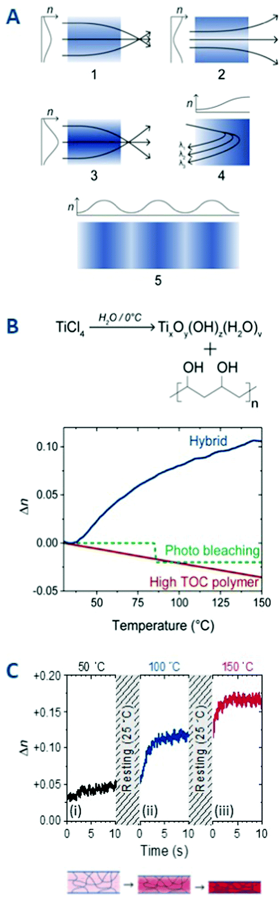 | ||
| Fig. 1 (A) Examples of how refractive index patterns can manipulate the flow of light: (1–3) Planar, graded refractive index lenses that focus or defocus light. The strength of refractive index modulation will change the focal length. (4) A graded index depth profile can be used as a selective mirror to de-multiplex a multiple wavelength input. (5) Sinusoidal diffractive element applicable to in- and out-coupling, distributed feedback, and for holographic data storage. (B) Molecular organic/inorganic hybrids are produced via a one-pot synthesis of titanium oxide hydrates from titanium tetrachloride, TiCl4, in the presence of a poly(vinyl alcohol) binder polymer.7,8 The chemical structure of the resulting material is shown in the ESI† (Fig. S1). On heating films, ≈630 nm thick and spin-coated from the reaction mixture, there is a significant increase in refractive index, n. Here, data for a hybrid composed of 60 vol% titanium oxide hydrate are shown upon heating at a rate of 20 °C min−1; blue line. For comparison, data for a common optical polymer with high thermo-optic coefficient is shown (ref. 9; red line), as well as for a plastic where a change in refractive index is achieved via photobleaching as described in ref. 13 (dashed green line). (C) Refractive index change of a hybrid film (≈350 nm at t = 0 s), deposited on a Si/SiO2 substrate, upon annealing at different temperatures on a pre-heated hot-plate. The following temperature cycle was performed: (i) annealing for 10 seconds to 50 °C, (ii) cooling to room temperature (which took approximately 5 min), (iii) annealing for 10 seconds to 100 °C, (iv) cooling to room temperature (length: ≈5 min), and (v) annealing for 10 seconds to 150 °C. | ||
We begin our analysis with an in situ assessment of the refractive index change, Δn, from a PVAl/titanium oxide hydrate hybrid sample subjected to a heating rate of 20 °C min−1. The sample comprised a 60 vol% inorganic content hybrid film (see Fig. 1B, bottom panel), a composition that has previously been found to provide an excellent compromise with respect to film formation, refractive index and optical quality,7,8 and that could be readily spin-coated onto a glass substrate. Optical transmittance spectra were recorded at 30 ms intervals, with a spectrometer linked to an optical microscope with the sample placed on a hotplate throughout the measurement to control its temperature (see Fig. S2, ESI,† top panel). The film thickness (typically ≈630 to ≈670 nm, though in some cases 350 nm was used) was sufficient to allow clear Fabry–Perot oscillations in the transmission spectra to be tracked during the experiment; these oscillations confirmed the low optical absorption and good-quality interfaces present in the film (Fig. S2, ESI,† bottom panel).
During heating, and as expected for an overall increase in optical path length, the Fabry–Perot oscillations blue shift and become more pronounced.8 At each temperature, the film thickness, d, and refractive index, n, at 550 nm were extracted from the spectra using a transfer-matrix method (TMM) (see ESI,† for details). Upon heating to 150 °C, we find that the refractive index of the film increases by +0.11. This change can be compared to that observed from currently used optical polymers, where Δn is typically negative (refractive index decreases upon heating) and often is as small as −0.03 for a temperature change of 100 °C;9–13 sample photo-bleaching and high thermo-optic coefficient (TOC) polymer data (taken from ref. 9, green, and ref. 13, red, respectively) are shown in the bottom panel of Fig. 1B. We note that large birefringence values can be generated in polymer-based materials by means other than heat: a Δn ≤ 0.36 was, for example, achieved by thermotropic liquid crystal polymer orientation but until recently such changes were not easy to spatially pattern.14 Photoalignment of films allow such patterning.15 Conformation control is another approach with Δn ≤ 0.3 and spatial resolution down to 0.5 μm using dip-pen nanolithography.16,17
As anticipated from the chemistry of the hybrid,7,8 we find a direct correlation between the refractive index increase and a material densification that occurs during heating.7,8 Throughout the process, the film remains securely attached to the substrate so that the densification manifests as a thickness reduction. We also note that this shrinkage does not visibly reduce the quality of the film. The specific relationship between the refractive index and the film thickness is determined by comparing the evolution of the n and d values deduced from in situ UV-vis transmittance measurements during heating (Fig. S3, ESI,† left panel). The resulting master curve for n versus percentage of 1-D contraction of the film then allows estimation of n from the measured change in thickness and vice versa (Fig. S3, ESI,† right panel).
A necessary requisite to produce well-defined optical features, such as arrays of refractive index patterns, is to limit any lateral heat flow. In this regard, the relatively short heating time required to convert the PVAl/titanium oxide hydrate hybrid films is notable. The response time may be inferred from repeated optical transmittance measurements as a function of time following a step change in temperature (Fig. 1C). A PVAl/titanium oxide hydrate hybrid film (with inorganic content = 60 vol%) was subjected to the following thermal cycle: (i) annealing for 10 seconds to 50 °C, (ii) cooling to room temperature (which approximately took 5 min), (iii) annealing for 10 seconds to 100 °C, (iv) cooling to room temperature (length: ≈5 min), and (v) annealing for 10 seconds to 150 °C. In addition to the fast response of order a few seconds that is observed at the higher temperatures, it is also noteworthy that the refractive index changes are additive: i.e., annealing a sample to 100 °C after a first heat treatment at 50 °C adds to the Δn achieved in the first step. The corresponding thickness changes are shown in Fig. S4 (ESI†).
Having the capability to induce different refractive indices in a material via rapid local heating, with Δn controlled by selection of annealing time/temperature, opens the possibility to produce refractive-index patterns for device application. For example, it should be possible to generate periodic changes in the refractive index to act as an optical grating to couple optical radiation into or out of a film or multilayer structure. A ‘four-quarter’ pattern was prepared by sequential contact heating with a pre-heated flat rectangular metallic stamp to provide a proof-of-concept demonstration of spatial patterning. The stamp, initially heated to T1 = 50 °C, was brought into contact by hand, for a period of 5 seconds, with half of the surface of a 60 vol% titanium oxide hydrate/PVAl hybrid film on glass. The sample was allowed to cool to room temperature before, once again, being contacted for 5 seconds with a stamp now heated to T2 = 100 °C. For this second step, the stamp was rotated by 90° thereby heating one previously heated quarter and one new quarter. The final step, with the stamp at T3 = 150 °C resulted in heating, for 5 seconds, the originally treated quarter for the third time. Fig. 2A shows a schematic illustration of the process; the resulting structure left one ‘pristine’ quarter that was not subjected to any heat.
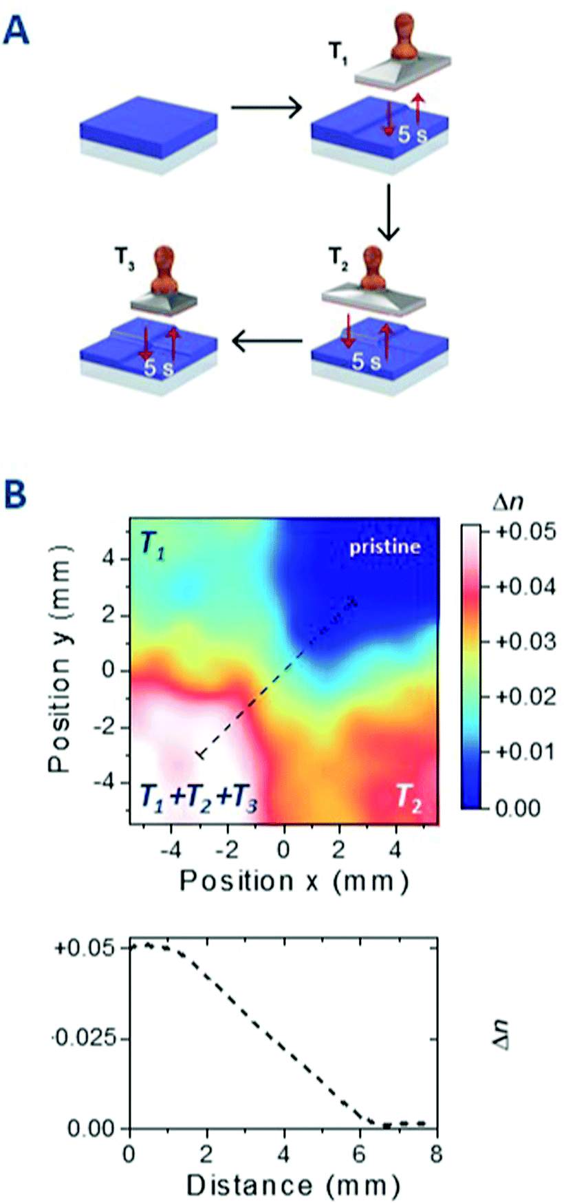 | ||
| Fig. 2 Proof of concept demonstration of spatial patterning of refractive index structures by sequential hot-stamping using ≈645 nm-thin films. (A) Schematic of the hot-stamping process. A pre-heated metal stamp is brought in direct contact with selected regions of the film for 5 second intervals. The stamp is heated at different temperatures at each step of the process (T1 = 50 °C, T2 = 100 °C and T3 = 150 °C) and the sample is then allowed to cool to room temperature after each hot-stamping step. The stamp can be reapplied in different orientations so that different areas are subjected to different time-temperature profiles. (B) Top panel: Plan-view map of n after successive heat-stamp process steps, showing the modulation in refractive index that can be realized. Spectra were measured spatially resolved across the entire sample and analysed via TMM. The corresponding thickness maps are shown in ESI† (Fig. S4). Bottom panel: An index change of Δn = 0.05 is measured along the diagonal (see top panel dotted line) between highest and lowest index regions with a smooth graded index (GI) profile. | ||
To spatially resolve the changes in the refractive index, a translation stage was employed to record the transmittance of the sample; the change in the refractive index at each position was then deduced. The four quarters are visible in the refractive index map (Fig. 2B, top panel; with corresponding thickness variations displayed in Fig. S5, ESI†). The average index differences relative to the unheated quarter are Δn ≈ 0.022 for 50 °C heated; Δn ≈ 0.035 for 100 °C heated; and Δn ≈ 0.050 for 50, 100 and 150 °C sequential heating.
While this preliminary test is limited in its sophistication, especially in terms of spatial resolution, it provides the desired proof-of-concept. The refractive index measured along a diagonal (Fig. 2B, top panel, dashed line) from the quarter heated to 150 °C to the unheated quarter, shows a smooth Δn gradient (Fig. 2B, bottom panel), with an overall Δn = 0.05.
More elegant and precise methods can be utilized to locally heat samples, particularly to improve spatial resolution. For example, scanning thermal lithography allows sub-micron resolution.18,19 Another approach is a photothermal annealing strategy20–23 that uses spatially controlled absorption of pulsed light from a Xenon flashlamp (Fig. 3A) and is capable of efficiently delivering heat over a larger area. Intrigued by this possibility, we have sought to test its utility for patterning the material family used here. The PVAl/titanium oxide hydrate hybrid material absorbs in the UV range (<300 nm). This does not match the lamp output which spans ≈300 to 1000 nm, thereby precluding direct absorptive heating through a shadow mask to define the pattern. Instead, a combined mask/absorber was formed which comprised aluminium lines of 100–200 nm thickness patterned atop a polydimethylsiloxane (PDMS) stamp on a glass substrate. The metal lines absorb the lamp output and when the mask is softly pressed onto the PVAl/titanium oxide hydrate film, it provides a means for localized heating (Fig. 3A). The Xenon lamp emits 1–1.6 ms duration, 4.8 kJ light pulses (see ESI†) and the stack was exposed to ten pulses, incident through the PDMS substrate. Where there is no metal present the lamp pulses pass straight through. Surface profilometry of the hybrid film after exposure showed a 15% densification (from 660 to 575 nm) for the region in contact with the metal, but no shrinkage elsewhere. The lateral transition width (resolution) was ≈100 μm (Fig. 3B).
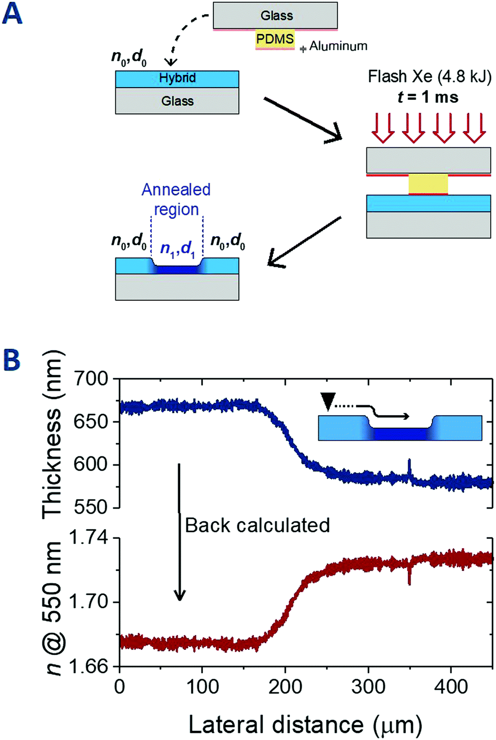 | ||
| Fig. 3 Microcontact photothermal annealing (μCPA) of PVAl/titanium oxide hydrate hybrid films (≈670 nm thickness) for refractive index patterning. (A) Illustration of the process that combines photothermal curing with micro-contact printing using a PDMS stamp coated with 100–200 nm thick aluminium lines. These lines absorb light and heat the hybrid sample when in direct contact therewith. (B) Surface profilometry data (blue line) quantifying the change in thickness (shrinkage) across a boundary between pristine (left) and photothermally heated (right) regions. No shrinkage is observed away from where the aluminium lines are in contact with the film. The corresponding data for n are also shown (red line), calculated using the linear relationship between n and d (Fig. S2, ESI†). | ||
Referring to the master curve established in Fig. S3 (ESI†), this change in thickness (d) corresponds to a refractive index change of 0.045 (i.e. from 1.678 for regions with no metal coating, to 1.723 where the material was in contact with the metal lines). Such localized index changes are more than adequate to provide a degree of lateral optical confinement as evident from the finite-element modelling of a simple channel waveguide structure, especially if a resolution of 1 μm were to be achieved in future (Fig. 4; see the ESI† for details).
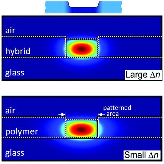 | ||
Fig. 4 Finite-element modelling (see ESI† for details) illustrating the improvement of energy localization in the intensity of the TE fundamental mode for a wavelength of 550 nm in a co-planar channel waveguide if a resolution of 1 μm were to be achieved via local annealing of the PVAl/titanium oxide hydrate hybrid (top panel). This is compared to currently used systems as described in, e.g., ref. 9–13 (bottom panel), assuming an air top cladding (n = 1) and a glass bottom cladding (n = 1.5185) in both scenarios. The central section was modelled with an index difference of +0.10 relative to the neighbouring areas (n = 1.73 for the core; n = 1.63 for the untreated regions), as achievable by heat treating the hybrid material, while Δn = 0.05 was used to model currently available optical polymers (core: n = 1.68, side cladding n = 1.63![[thin space (1/6-em)]](https://www.rsc.org/images/entities/char_2009.gif) 9–13). Dimensions used were based on a high-refractive index core of 1 micron width and 575 nm in height (in case of the hybrid to take the shrinkage upon heat exposure into account; the height used for the untreated areas was 660 nm, vs. a 660 nm height for the whole structure for the reference polymer material). 9–13). Dimensions used were based on a high-refractive index core of 1 micron width and 575 nm in height (in case of the hybrid to take the shrinkage upon heat exposure into account; the height used for the untreated areas was 660 nm, vs. a 660 nm height for the whole structure for the reference polymer material). | ||
Having demonstrated the μCPA principle, we note that a variety of parameters for μCPA can be readily tuned to allow further optimisation of the process. These include the lamp pulse energy and duration, the number of pulses for each exposure step, along with the thickness and composition of the absorbing layer. Moreover, microcontact printing can also be used to diffuse gain materials into a polymer matrix film,24 which would add further versatility to the approach outlined here, in potentially enabling the construction of high-resolution active optical structures.
Conclusions
We have demonstrated the use of μCPA in the fabrication of laterally patterned refractive-index structures using a PVAl/titanium oxide hydrate hybrid material family. This approach is shown to allow patterning times of less than a second, often a few micro-seconds, with the potential for shorter times still. This is combined with a refractive index change, Δn, of +0.05 that is higher than what is achieved with25 or equal to26 previously reported polymer-based systems via thermal patterning. However, for those latter materials,25,26 the patterning time required was in the range of 10 min,25 or a highly specialized equipment such as a near-field scanning optical microscope was needed.26 We also like to point out that the hybrid used here can be synthesized with a very simple one-pot synthesis and the refractive index (as well as Δn) can be varied via the content of the inorganic species,7,8 while the systems in, e.g., ref. 25 and 26 are less versatile. The simplicity and versatility of the hybrid synthesis and processing may also make our platform competitive to inorganic materials where notably higher Δn can be realized but are produced, e.g., via processes such as electrochemical etching using in some instances ethanoic hydrofluoric acid, followed by compression at pressures as high as 400 N mm−2,27 which in comparison to the work here seems to be tedious and time consuming. Compared to inorganic materials,27,28 the PVAl/titanium oxide hydrates hybrid material can, moreover, be expected to be mechanically significantly more robust, especially if higher molecular-weight PVAl is used for their production. The promise of the PVAl/titanium oxide hydrates hybrid material patterned with μCPA is that they enable simple, ultra-fast fabrication of complex refractive-index patterns in mechanically robust materials.7 Hence, guided-wave photonic structures on a wide range of substrates may be realized including those that are thermally sensitive such as plastics, opening a new strategy for developing ubiquitous, flexible photonics.Author contributions
SB performed most of the experiments in this work including hybrid material synthesis, processing and optical materials characterization. HKY conducted the optical modelling, while KT assisted with the photocuring, advised by TDA and DDCB. PNS oversaw the optical characterization and modelling aspects. SB and NS prepared the draft manuscript which was revised by DDCB, PNS and NS and commented on by all other authors. NS and PNS designed the research.Conflicts of interest
There are no conflicts to declare.Acknowledgements
We like to thank Dr J. Gebers and Dr A. Hafner, from BASF Schweiz for highly valuable discussion, and Dr Irene Votta for materials characterization. WSB, HKY, PS, DDCB and NS thank the UK's Engineering and Physical Sciences Research Council (EPSRC) for funding via the Centre for Doctoral Training in Plastic Electronics Materials, PE-CDT (EP/G037515/1). SB, HKY, DDCB, PS and NS furthermore acknowledge funding provided by BASF Schweiz AG towards this PE-CDT project. NS and PS are, moreover, grateful for support by the Marie Skłodowska-Curie Actions Innovative Training Network “H2020-MSCAITN-2014 INFORM – 675867”. KT and TDA acknowledge the financial support from the People Programme (Marie Curie Actions) of the European Union's Framework Programme Horizon 2020: “Flexible Complementary Hybrid Integrated Circuits” (FlexCHIC), Grant Agreement No. 658563. Finally, NS acknowledges further support by the U.S. National Science Foundation (DMR #1838276).References
- H. Ma, A. K.-Y. Jen and L. R. Dalton, Adv. Mater., 2002, 14, 1339 CrossRef CAS.
- A. Tervonen, S. K. Honkanen and B. R. West, Opt. Eng., 2011, 50, 071107 CrossRef.
- W. Hong, H.-J. Woo, H.-W. Choi, Y.-S. Kim and G. Kim, Appl. Surf. Sci., 2001, 169–170, 428 CrossRef CAS.
- A. Zakery and S. R. Elliott, J. Non-Cryst. Solids, 2003, 330, 1 CrossRef CAS.
- X. Mao, S.-C. S. Lin, M. I. Lapsley, J. Shi, B. K. Juluri and T. J. Huang, Lab Chip, 2009, 9, 2050 RSC.
- H. Huang, X. Mao, S.-C. S. Lin, B. Kiraly, Y. Huang and T. J. Huang, Lab Chip, 2010, 10, 2387 RSC.
- M. Russo, M. Campoy-Quiles, P. Lacharmoise, T. A. M. Ferenczi, M. Garriga, W. R. Caseri and N. Stingelin, J. Polym. Sci., Part B: Polym. Phys., 2012, 50, 65 CrossRef CAS.
- S. Bachevillier, H.-K. Yuan, A. Strang, A. Levitsky, G. L. Frey, A. Hafner, D. D. C. Bradley, P. N. Stavrinou and N. Stingelin, Adv. Funct. Mater., 2019, 29, 1808152 CrossRef.
- M.-C. Oh, W.-S. Chu, J.-S. Shin, J.-W. Kim, K.-J. Kim, J.-K. Seo, H.-K. Lee, Y.-O. Noh and H.-J. Lee, Opt. Commun., 2016, 362, 3 CrossRef CAS.
- Z. Zhang and N. Keil, Opt. Commun., 2016, 362, 101 CrossRef CAS.
- M. Nakanishi, O. Sugihara, N. Okamoto and K. Hirota, Appl. Opt., 1998, 37, 1068 CrossRef CAS.
- S. Shibata, O. Sugihara, Y. Che, H. Fujimura, C. Egami and N. Okamoto, Opt. Mater., 2003, 21, 495 CrossRef CAS.
- D. B. Wolfe, J. C. Love, B. D. Gates, G. M. Whitesides, R. S. Conroy and M. Prentiss, Appl. Phys. Lett., 2004, 84, 1623 CrossRef CAS.
- T. Virgili, D. G. Lidzey, M. Grell, S. Walker, A. Asimakis and D. D. C. Bradley, Chem. Phys. Lett., 2001, 341, 219 CrossRef CAS.
- Y. Shi, P. S. Salter, M. Li, R. A. Taylor, S. J. Elston, S. M. Morris and D. D. C. Bradley, Adv. Funct. Mater., 2020, 2007493 Search PubMed.
- P. N. Stavrinou, G. Ryu, M. Campoy-Quiles and D. D. C. Bradley, J. Phys.: Condens. Matter, 2008, 19, 466107 CrossRef.
- A. Perevedentsev, Y. Sonnefraud, S. Sharma, A. E. G. Cass, S. A. Maier, J. S. Kim, P. N. Stavrinou and D. D. C. Bradley, Nat. Commun., 2015, 6, 5977 CrossRef CAS.
- J. E. Shaw, P. N. Stavrinou and T. D. Anthopoulos, Adv. Mater., 2013, 25, 552 CrossRef CAS PubMed.
- J. E. Shaw, P. N. Stavrinou and T. D. Anthopoulos, Nanoscale, 2014, 6, 5813 RSC.
- T.-H. Yoo, S.-J. Kwon, H.-S. Kim, J.-M. Hong, J. A. Lim and Y.-W. Song, RSC Adv., 2014, 4, 19375 RSC.
- W. H. Lee, S. J. Lee, J. A. Lim and J. H. Cho, RSC Adv., 2015, 5, 78655 RSC.
- C. Kang, H. Kim, Y. W. Oh, K. H. Baek and L. M. Do, IEEE Electron Device Lett., 2016, 37, 595 CAS.
- K. Tetzner, Y.-H. Lin, A. Regoutz, A. Seitkhan, D. J. Payne and T. D. Anthopoulos, J. Mater. Chem. C, 2017, 5, 11724 RSC.
- M. C. Ramon Lorente De No, Polymer Dispersed Dyes as Gain Media for Optical Amplifiers and Lasers, PhD thesis, Imperial College, London, 2005.
- T. S. Kleine, J. I. Frish, N. G. Pavlopoulos, S. A. Showghi, R. Himmelhuber, R. A. Norwood and J. Pyun, ACS Macro Lett., 2020, 9, 416 CrossRef CAS.
- Y. Kato, H. Muta, S. Takahashi, K. Horie and T. Nagai, Polym. J., 2001, 33, 868 CrossRef CAS.
- T. H. Talukdar, J. C. Perez and J. D. Ryckman, ACS Appl. Nano Mater., 2020, 3, 7377 CrossRef CAS.
- M. Kang, L. Sisken, J. Cook, C. Blanco, M. C. Richardson, I. Mingareev and K. Richardson, Opt. Mater. Express, 2018, 8, 330083 Search PubMed.
Footnote |
| † Electronic supplementary information (ESI) available. See DOI: 10.1039/d1mh01366a |
| This journal is © The Royal Society of Chemistry 2022 |