
Printing fabrication of large-area non-fullerene organic solar cells
Peiyao
Xue
a,
Pei
Cheng
 b,
Ray P. S.
Han
*a and
Xiaowei
Zhan
*a
b,
Ray P. S.
Han
*a and
Xiaowei
Zhan
*a
aKey Laboratory of Polymer Chemistry and Physics of Ministry of Education, School of Materials Science and Engineering, Peking University, Beijing, 100871, P. R. China. E-mail: ray-han@pku.edu.cn; xwzhan@pku.edu.cn
bCollege of Polymer Science and Engineering, Sichuan University, Chengdu, 610065, P. R. China
First published on 29th September 2021
Abstract
Organic solar cells (OSCs) based on a bulk heterojunction structure exhibit inherent advantages, such as low cost, light weight, mechanical flexibility, and easy processing, and they are emerging as a potential renewable energy technology. However, most studies are focused on lab-scale, small-area (<1 cm2) devices. Large-area (>1 cm2) OSCs still exhibit considerable efficiency loss during upscaling from small-area to large-area, which is a big challenge. In recent years, along with the rapid development of high-performance non-fullerene acceptors, many researchers have focused on developing large-area non-fullerene-based devices and modules. There are three essential issues in upscaling OSCs from small-area to large-area: fabrication technology, equipment development, and device component processing strategy. In this review, the challenges and solutions in fabricating high-performance large-area OSCs are discussed in terms of the abovementioned three aspects. In addition, the recent progress of large-area OSCs based on non-fullerene electron acceptors is summarized.
 Peiyao Xue | Peiyao Xue received her BS degree in materials science and engineering from Tianjin University in 2017. Now she is a PhD student in Peking University. Her research interests focus on the fabrication of organic solar cells. |
 Pei Cheng | Pei Cheng received his BE in Polymer Materials and Engineering from Sichuan University in 2011. He then joined Prof. Xiaowei Zhan's group at the Institute of Chemistry, Chinese Academy of Sciences (ICCAS)/Peking University, and received his PhD in Chemistry (2016). Dr Cheng worked in Prof. Yang Yang's group in the Department of Materials Science and Engineering at the University of California, Los Angeles from 2017 to 2020 as a Postdoc Researcher. He is currently a professor at Sichuan University. His research interests are focused on organic solar cells. |
 Ray P. S. Han | Ray P. S. Han received his PhD from the University of British Columbia. He is a professor of materials science and engineering at Peking University. His research is focused on flexible electrodes for flexible Li-ion batteries and supercapacitors, harvesting ambient nano–mesoscale energy for self-powered sensors and devices, and nano–microfluidic devices. |
 Xiaowei Zhan | Xiaowei Zhan received his PhD in polymer chemistry from Zhejiang University in 1998. He was then a postdoctoral researcher and an associate professor at ICCAS from 1998 to 2002. Dr Zhan worked at the University of Arizona and Georgia Institute of Technology from 2002 to 2006 as a research associate/scientist. He has been a full professor at ICCAS since 2006 and joined Peking University in 2012. His research interests are in the development of materials for organic electronics and photonics. |
1. Introduction
Solar cells are an attractive technology to harvest inexhaustible renewable clean energy from the sun. Organic solar cells (OSCs), as a next-generation photovoltaic technology alternative to traditional silicon-based ones, possess several advantages, such as low cost, light weight, mechanical flexibility and short energy payback time.1,2 The first OSC was invented in 1958, in which magnesium phthalocyanine was the single-component active layer, and yielded a very low open-circuit voltage (VOC) of only 0.2 V.3 In 1986, Tang4 invented a bilayer OSC, in which the donor (copper phthalocyanine) and the acceptor (a perylene tetracarboxylic derivative) were separately vacuum-deposited. The bulk heterojunction structure was invented in the 1990s,5–7 which developed into one of the most efficient device structures in organic solar cells. A sufficient donor/acceptor interface along with an ideal bicontinuous interpenetrating network is beneficial for exciton dissociation and charge transport.Fullerene acceptors such as PC61BM (phenyl-C61-butyric acid methyl ester) and PC71BM (phenyl-C71-butyric acid methyl ester) have dominated the OSC field over 20 years, since they have some unique advantages, such as high electron affinity and isotropic electron-transporting ability with high electron mobility, which are beneficial for charge separation and charge transport. However, their weak light absorption in the visible and near-infrared (NIR) regions, morphological instability and large energy loss limited further development of the OSC field.8 The maximum theoretical power conversion efficiency (PCE) of fullerene-based OSCs is ∼13%.9 In 2015, the Zhan group invented a high-performance non-fullerene acceptor, the star molecule ITIC,10 then pioneered the concept of “fused-ring electron acceptors” (FREAs).11–13 FREAs generally consist of an electron-donating fused-ring core, electron-accepting end groups, π-bridges and side chains. Molecular structure modularity benefits chemical tailoring and property modulation. The strong intramolecular charge transfer between the fused-ring core and terminal groups enhances light absorption, especially in the 700–1000 nm region. The planar and rigid molecular backbone reduces energy disorder and reorganization energy and facilitates charge transport. Out-of-plane side chains effectively adjust the molecular packing and prevent excessive aggregation, which is beneficial for suitable phase separation and morphological stability. As a result, FREA-based OSCs show low voltage loss, high efficiency and good stability.12 Up until now, thousands of FREAs have been synthesized,14–21 and the champion PCEs of FREA-based OSCs exceed 18%.22–24 Except for high PCE values, the unique optical and electrical properties of FREAs endow them with great application potential. FREAs show strong NIR absorption, which is suitable for fabricating rear active layers of tandem devices25–28 and semi-transparent or even fully transparent devices suitable for implementation in buildings and windows or greenhouse agrivoltaics.29–37 FREAs have long exciton diffusion lengths and high electron mobilities, which are beneficial for fabricating thick-film and large-area devices.38–40 Furthermore, FREAs can also be used in photodetectors41 and other electronic devices, exhibiting great application potentials.12
Some groups focused on developing large-area scalable OSCs. In 2009, Krebs et al.42 reported fully roll-to-roll (R2R) processed OSCs with an inverted architecture of polyethylene terephthalate (PET)/indium tin oxide (ITO)/zinc oxide (ZnO)/photoactive layer/poly(3,4-ethylenedioxythiophene):poly(styrenesulfonate) (PEDOT:PSS)/silver (Ag), which is referred to as “ProcessOne”. ProcessOne mainly contains five steps, including etching pretreatment, slot-die coating of the ZnO layer, active layer and PEDOT:PSS layer and screen printing of the silver electrode. Many reported large-scale OSC devices and modules are based on this R2R process.43,44
Compared with small-area OSCs, large-area OSCs still exhibit relatively lower PCE values. Most large-area OSCs are based on fullerene acceptors, which have been summarized in some reviews.45–54 In recent years, along with the rapid development of high-performance non-fullerene acceptors, more research groups started to fabricate large-area devices and modules based on emerging non-fullerene acceptors.55 Since non-fullerene acceptors exhibit different packing and aggregation behaviors compared with fullerene acceptors, new methods for the construction of high-performance non-fullerene-based large-area OSCs are highly desired. In this review, we discussed the challenges and solutions in fabricating high-performance large-area OSCs in terms of three aspects: fabrication technology, equipment development and device component processing strategy. In addition, we summarized the progress of printed OSCs based on non-fullerene electron acceptors, especially FREAs.
2. Large-area fabrication technologies: printing and coating
Large-area OSCs are generally fabricated by addition-, subtraction-, and pattern-based manufacturing technologies. The widely used methods, including printing, coating and vacuum evaporation, belong to addition-based technology, where additional components are added onto the substrates and basic substrates have not been damaged. Laser ablation and photolithography belong to subtraction-based technology, where partial materials are removed from the substrates, and are usually used in large-area module fabrication. The third one is pattern-based technology, including wetting/de-wetting, imprinting or bonding methods.Among the addition-based manufacturing technologies, solution processing (printing/coating) is the most convenient. Printing (including screen printing, gravure printing, flexographic printing, pad printing, offset printing and so on) is a stamping process, where a complex two-dimensional (2D) pattern can be formed. Comparatively, coating is a simple and direct film-forming technology, where a simple zero-dimensional or one-dimensional pattern can be formed. Coating technologies mainly include casting, spin coating, spray coating, doctor blade coating, slot-die coating, knife-over-edge coating, and floating film transfer methods. Inkjet printing is a coating technology but is capable of producing complex 2D patterns.
2.1 Single-substrate fabrication
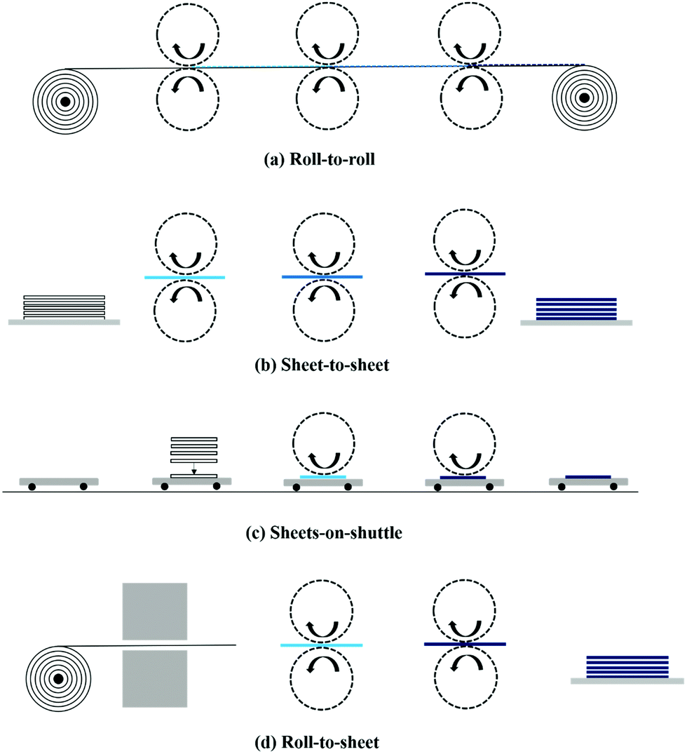
For single-substrate fabrication, the active layer is printed or coated onto an isolated rigid/flexible substrate. According to the principle of transferring materials onto the substrate, the printing and coating technologies can be classified into of non-contact and contact.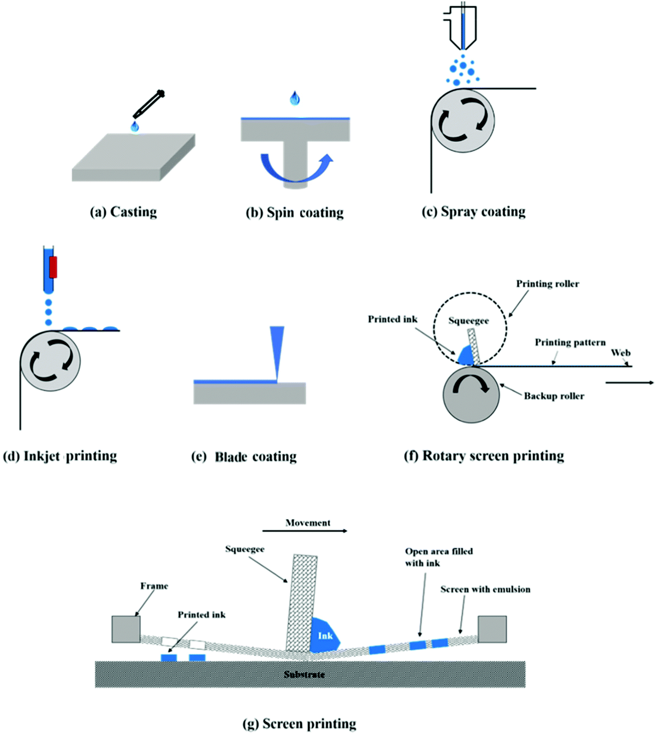 | ||
| Fig. 1 Single substrate-based fabrication technologies. Reproduced with permission.47 Copyright 2020, the authors, under the Creative Commons Attribution 3.0 license (c and d). Reproduced with permission.45 Copyright 2009, Elsevier (f and g). | ||
Spin coating is a contact/non-contact fabrication technology (Fig. 1b); a certain amount of ink is dropped onto the substrate, followed by spinning the substrate at a certain speed. Alternatively, the liquid solution can be dropped while the substrate is spinning. During the spinning, most of the solution is ejected or volatilized, and only a thin film remains on the substrate. Film thickness and surface/bulk morphology are highly related to spinning speed, ink concentration, ink viscosity and ink volatility. The film thickness can be expressed by the empirical relationship:
| d = kωα, | (1) |
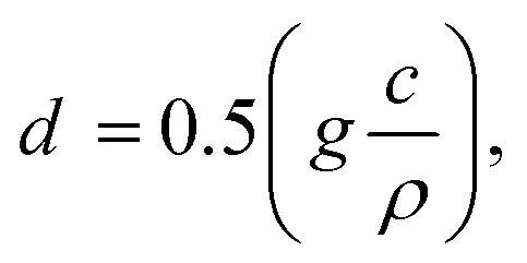
Spray coating is a non-contact, R2R compatible fabrication technology (Fig. 1c); the ink is sprayed through a nozzle and a fine aerosol is formed.58,59 Generally, spray coating is composed of four steps:60 liquid atomization,61 in-flight droplet evaporation,62 drop impact on the surface63 and droplet drying. This kind of technology exhibits good ink generality with a wide range of viscosity and volatility of spraying ink. In order to direct the aerosol to the expected location to form patterns, a carrier gas and a pair of electrostatic charging parallel plates are often adopted. The drawback of spray coating is the uncontrollable film smoothness. To form a uniform film, the aerosol droplets have to spread uniformly upon reaching the substrate, which is difficult to be guaranteed. As a result, this method is not frequently used in practical R2R fabrication.
Inkjet printing is a non-contact and high-material-utilization fabrication technology, beneficial for printing various functional layers (Fig. 1d). It involves two steps, ejecting inks from the nozzle to form droplets and forming precise patterns on the target substrate under control.64–67 According to different droplet generation principles, inkjet printing is divided into continuous inkjet printing (CIP) and drop-on-demand (DoD) inkjet printing (Fig. 2). CIP is a non-stop flow ejection through the nozzle. The ink fluid is firstly ejected from the nozzle and breaks into a column of droplets owing to Rayleigh instability. Then, with droplets falling down, they are partly charged by a pair of parallel charging electrodes. The charged droplets are influenced by the dual effect of gravity and electric force, steering towards the targeted position to form patterns. DoD inkjet printing is a more popular method compared with CIP owing to less ink waste and more precise pattern resolution. It can achieve 5000 dots per inch with fine adjustment of the nozzle diameter in the range of 20–100 μm.46 Droplet formation is controlled by a sudden chamber volume change, digitally controlled by mechanical deformation of a piezoelectric transducer or mechanical collapse of thermal bubbles. As a result, DoD inkjet printing can be divided into piezoelectric and thermal DoD inkjet printing.
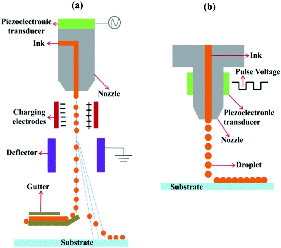 | ||
| Fig. 2 Schematic illustration of two kinds of inkjet printing methods: (a) CIP and (b) DoD inkjet printing. Adapted with permission.67 Copyright 2019, The Royal Society of Chemistry. | ||
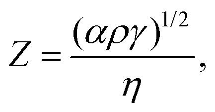
Ink formulation is important for inkjet printing, which is highly related to the formation of stable droplets. A dimensionless parameter Z is adopted to characterize the formation of a stable droplet:
 | (2) |
 | (3) |
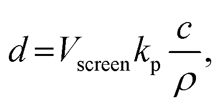
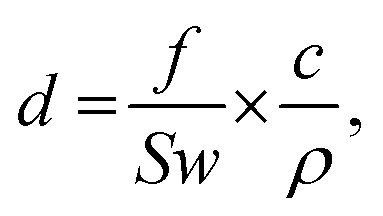
Screen printing is a versatile printing technology, suitable for 2D patterning of printed layers. It uses a steel mesh or an artificial fiber screen. There are many empty areas on the screen, which can be filled by the deposited ink. A squeegee linearly moves along the screen, pressing the ink onto the empty areas to form patterns. As a result, the layer thickness is correlated with the screen volume, which can be empirically expressed as
 | (4) |
2.2 Series-substrate fabrication
 | ||
| Fig. 3 Illustration of substrate transport types. Reproduced with permission.70 Copyright 2014, the authors, under the CC BY-NC-ND 3.0 license. | ||
 | ||
| Fig. 4 Series-substrate fabrication technologies. Reproduced with permission.47 Copyright 2020, the authors, under the Creative Commons Attribution 3.0 license (b). Reproduced with permission.45 Copyright 2009, Elsevier (a, c and d). | ||
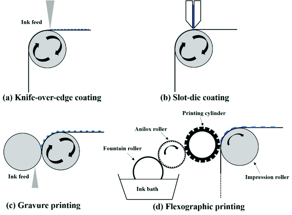
Knife-over-edge coating is a zero-dimensional coating method, similar to blade coating, in which the knife is fixed at a certain distance towards the supporting roller and the web is moving (Fig. 4a). Excessive ink is gradually added to a bath downstream of the knife.
Slot-die coating is a one-dimensional coating technology, in which one or more stripes with well-defined widths can be formed (Fig. 4b), and can meet the demand of a high degree of patterning in upscaling fabrication. The ink is supplied by a pump or a pressure system to a steel-made coating head, and it is deposited through a well-patterned mask to the moving substrate. The most important part in a slot-die head is a well-designed mask defining the slots and voids in the coating head. Generally, the slot-die head is equipped with a meniscus guide, which is used to control the striped pattern and edge quality of different layers. Fig. 5a shows a well-patterned coating mask with a meniscus guide comprising 5 stripes with a width of 12 mm spaced at 3 mm.71 The mask thickness is usually in the range of 20–50 μm. Another important component is the pump system. Peristaltic and piston pumps are used for inks with low viscosity (such as organic active layer and ZnO nanoparticles), and pressure tank pumps are used for relatively viscous pastes (such as Ag pastes).72
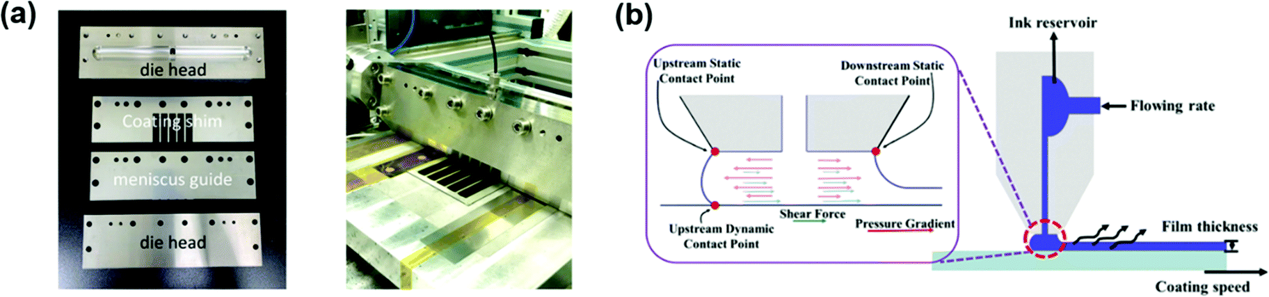 | ||
| Fig. 5 (a) A slot-die coater equipped with a coating shim and a meniscus guide. Adapted with permission.71 Copyright 2019, Elsevier. (b) Illustration of the stable meniscus formed. Adapted with permission.73 Copyright 2019, Elsevier. | ||
In order to get a well-distributed large-area film, forming a standing meniscus which lies between the moving substrate and coating head is important (Fig. 5b).73 Generally, slot-die coating is forgiving in ink viscosity. The ink solution usually possesses a low viscosity in the range of 1–20 cP. When using relatively viscous solutions (>100 cP), adopting a high coating speed (>10 m min−1) is a useful method to get a standing meniscus. Besides, adjusting the liquid feeding rate, ink flow rate, and ink concentration can work as well. The film thickness can be expressed as follows:
 | (5) |
Gravure printing is a more complex version of knife-over-edge coating and offers high-throughput, high-resolution, and high-quality patterning (Fig. 4c). It contains two rollers, a coating roller with an engraved pattern and a support roller with guiding the web. Generally, the print patterns are engraved into the coating roller through laser patterning, chemical etching or electromechanical etching. A high resolution of 20 μm can be realized. In a continuous R2R system, the coating roller is partly inserted into an ink bath. As the coating roller rotates in the ink bath, the engraved cells can be filled with ink. Excessive ink is knifed off the roller. While the coating roller is contacting with the support roller, the ink is transferred from the gravures onto the substrate under high printing pressure (usually 1–5 MPa). The efficiency of gravure printing is highly related to printing parameters (printing speed, printing pressure), engraved coating roller parameters (cell volume, cell depth, wall width, channel width, tone, screen angle, line density and stylus angle) and ink properties.74–77 Among the engraved coating roller parameters, line density is the most important parameter for thickness control. The lower the line density, the larger the cell volume and the thicker the film. Compared with other printing methods, gravure printing is suitable for low-viscosity ink solutions (10–1000 cP), high-speed processing and 2D patterning.
Flexographic printing is a 2D patterning technology which is an analogue of gravure printing. The ink transfer is performed from a relief opposed to cavities and the final pattern is formed over the printing plate. Typical flexographic printing is composed of four rollers (Fig. 4d). A fountain roller is partly immersed in the ink bath and touches an anilox roller, which has a well-defined engraved pattern. After that, the ink is transferred from the anilox roller to the printing roller, and then from the printing roller to the impression roller. This continuous R2R setup has similar advantages and limitations to gravure printing. Gravure printing and flexographic printing technologies have different application situations. The main differences between gravure printing and flexographic printing include the ink transfer pathway, printing speed, printed stripe thickness and ink viscosity. Flexographic printing uses a plate with a raised surface and fast drying fluid inks to print directly onto the desired substrate. Gravure printing is an intaglio printing process. The print patterns are engraved into the coating roller, and when the coating roller is contacting with a support roller, the ink is transferred from the gravures onto the substrate under high printing pressure. Furthermore, flexographic printing exhibits a slower printing speed (ca. 500 m min−1) compared with gravure printing (ca. 1000 m min−1), as well as thinner printed stripes (<1 μm in flexographic and ≈1 μm in gravure). The ink viscosity in flexographic printing (ca. 50–500 cP) is usually lower than that used in gravure printing (ca. 100–1000 cP).78 Flexographic printing is suitable for inks with high volatility because there is a closed ink chamber.
The floating film transfer method is an ultrafast, scalable and versatile printing technology for forming high-quality organic films by utilizing the Marangoni effect.79–82 A polymer solution with a low surface energy is self-spreading at the water interface with a high surface energy. The spontaneous spreading is called the Marangoni flow. The spreading coefficient (S) dictates the spreading flow:
| S = γ1 − γ2 − γ12, | (6) |
Here, we summarize the different characteristics of coating/printing technologies discussed above (Table 1), in terms of ink waste, pattern, coating/printing speed, ink viscosity requirements and contact between ink and substrates.
| Technique | Ink waste | Patterna | Speed | Ink viscosity | Contact |
|---|---|---|---|---|---|
| a Pattern: 0 (0-dimensional); 1 (1-dimensional); 2 (2-dimensional). | |||||
| Casting | Low | 0 | — | Low | No |
| Spin coating | High | 0 | — | Low | Yes/no |
| Spray coating | Medium | 0 | Medium | Medium | No |
| Inkjet printing | Low | 2 | Medium | Low | No |
| Blade coating | Low | 0 | Low | Low | Yes |
| Screen printing | Low | 2 | Medium | High | Yes |
| Knife-over-edge coating | Low | 0 | Medium | High | Yes |
| Slot-die coating | Low | 1 | High | Relatively high | Yes |
| Gravure printing | Low | 2 | High | Relatively low | Yes |
| Flexographic printing | Low | 2 | High | Relatively low | Yes |
| Floating film transfer | Low | 0 | High | Medium | Yes |
3. Large-area fabrication: equipment and module design
3.1 Production equipment
Lab-to-fab upscaling requires not only scaling of fabrication technology, but also scaling of equipment. In the lab-stage, desktop-based systems are adopted to test new fabrication technologies. The model is of a small size and can be put into a glove box for nitrogen atmosphere protection conditions. Fig. 6a–c show lab-scale flatbed coating systems for slot-die coating, screen printing, and gravure printing machines, respectively.84–86 For example, Lee et al.84 conducted a desktop-based lab-scale slot-die coating system with an equipment of Easy Coater (Solarcoating Machinery Gmbh, Germany). The coating speed varies from 0.3 to 5.0 m min−1, and the temperature of the substrate can be controlled by applying extra heat to the vacuum plate. Krebs et al.85 adopted a flatbed screen printing system to fabricate over 2000 modules in 63.3 hours (Fig. 7). Generally, the drying unit and the encapsulation unit are separated from the printing unit. These desktop-based small machines can realize a very high production speed with sheet-to-sheet printing. For example, Nelson et al.87,88 adopted a Schläfli Labratester table-top gravure printing machine to realize fast sheet-to-sheet fabrication. The speed of gravure printing proofers is 40–60 m min−1. The drying time varies from several minutes to hours. Because desktop-based testing machines lack the integration of the printing unit and drying unit, it cannot be directly used in a R2R-based system.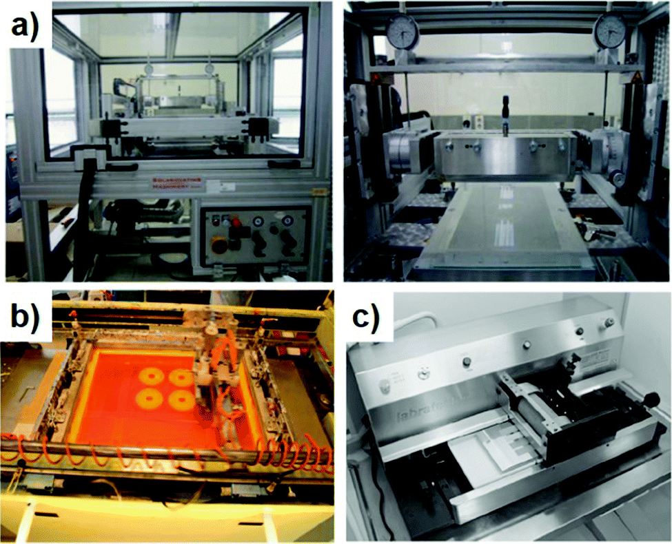 | ||
| Fig. 6 (a) Easy Coater (Solarcoating Machinery Gmbh, left) and slot-die head (right). Adapted with permission.84 Copyright 2013, Elsevier. (b) Flatbed screen printing machine. Adapted with permission.85 Copyright 2009, Elsevier. (c) Schläfli Labratester table-top gravure printing machine. Adapted with permission.86 Copyright 2010, Elsevier. | ||
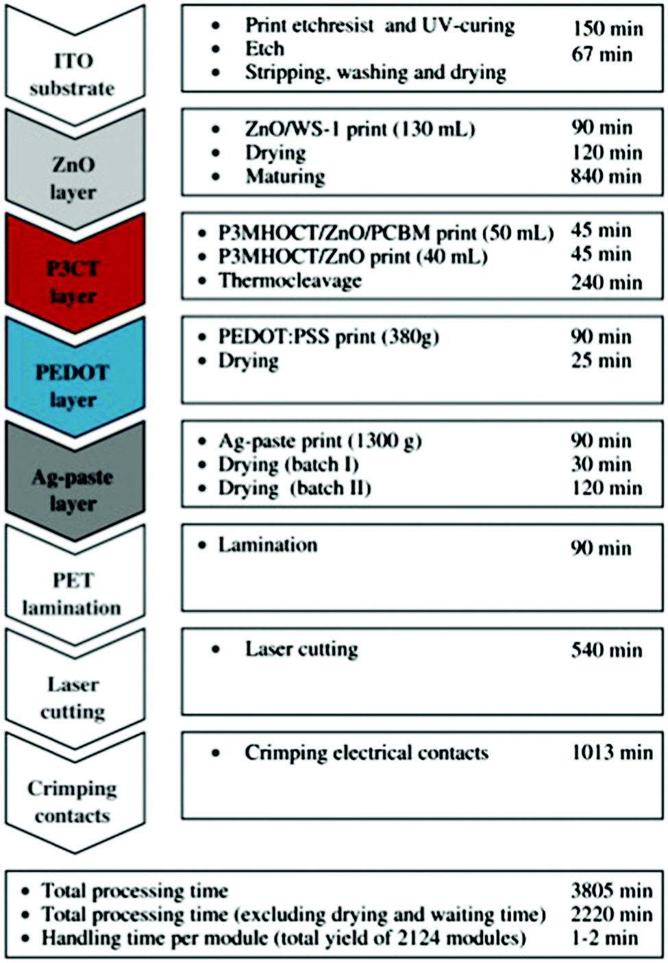 | ||
| Fig. 7 A process flow chart outlining all the steps employed in a flatbed screen printing system. Adapted with permission.85 Copyright 2009, Elsevier. | ||
The development of R2R-based systems is divided into three stages: mini single roll-coater, mini R2R coater, and large-scale R2R machine. The mini single roll-coater was invented by Krebs’ group (Fig. 8a), which mimics the coating performed on scalable R2R processing.89 The system is composed of a drum rolling (diameter = 300 nm), a servomotor (speed varies between 0 and 2 m min−1), a slot-die coating head (dead volume is less than 50 μL) and a syringe pump system. The rolling drum is automatically heated (up to 140 °C) to meet the demand of film drying and film post-annealing. Fig. 8b shows an improved version of the above-mentioned equipment. Krebs et al.90 assembled a slot-die coater and a flexographic printer into one mini-roller setup and realized full solution processing. Interfacial layers and the active layer were printed using a slot-die coater, and the back electrode (Ag pastes) was fabricated by flexographic printing. This kind of mini roll coater is successfully employed to test new organic materials.91,92
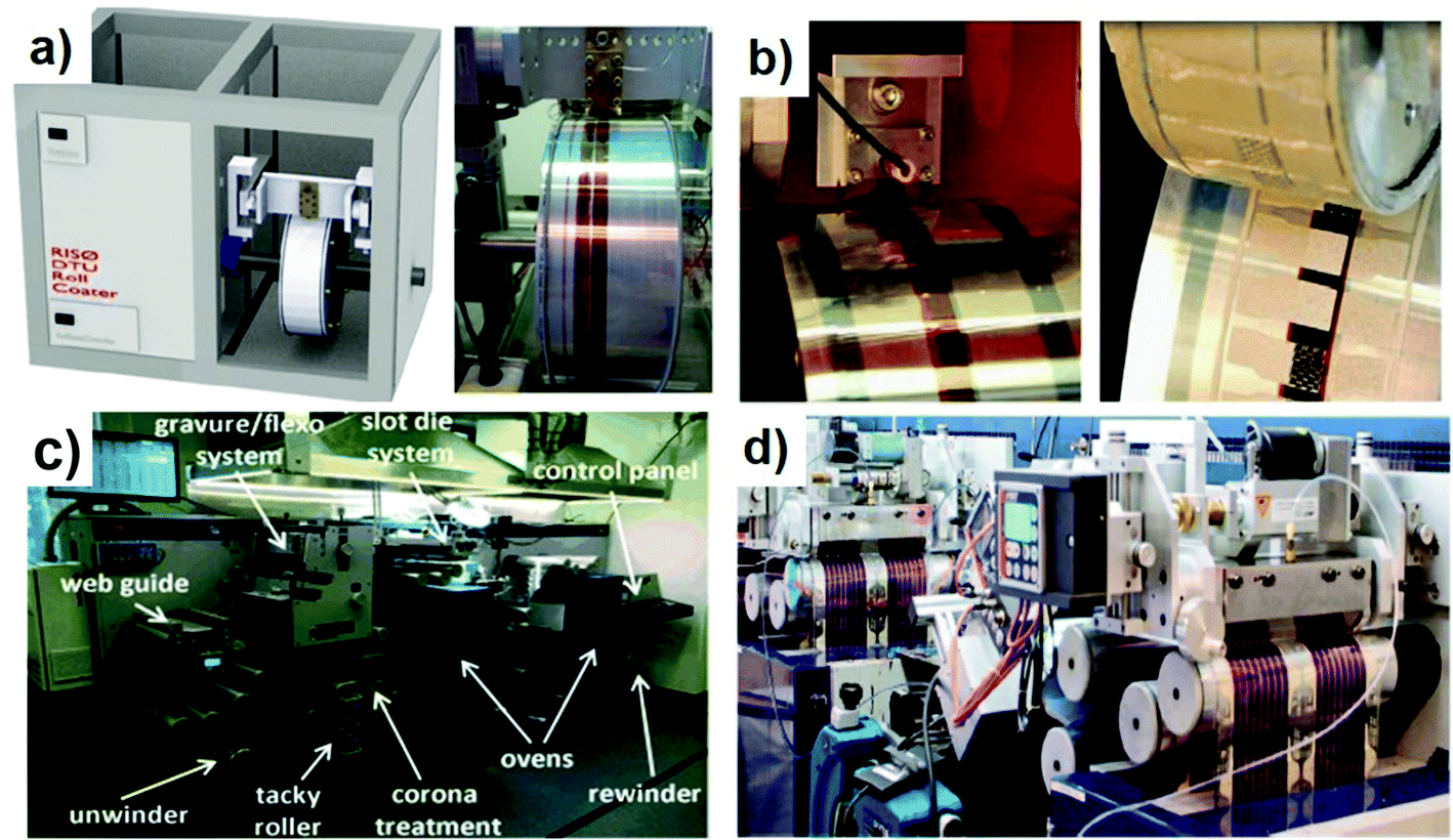 | ||
| Fig. 8 (a) A mini-roll coater from Technical University of Denmark. Adapted with permission.89 Copyright 2012, Elsevier. (b) A slot-die coater and a flexographic printer integrated into one mini-roller setup. Adapted with permission.90 Copyright 2013, Elsevier. (c) Solar-1 coating line from Grafisk Maskinfabrik. Adapted with permission.93 Copyright 2015, Wiley-VCH Verlag GmbH & Co. KGaA. (d) A fab-scale R2R printing and coating machinery. Adapted with permission.94 Copyright 2014, The Royal of Society Chemistry. | ||
The next stage is improving web width and printing speed, in which the printing unit and the drying unit should be integrated into one production line. The solar-1 coating line from Grafisk Maskinfabrik is the first fully automated R2R production line. It consists of a web alignment feedback control unit, a gravure and flexographic printing unit, a slot-die coating unit, and two integrated heating ovens (Fig. 8c).93 In this equipment, film deposition and in-line thermal post-treatment can be realized in a single printing cycle. This machine allows fast printing with a speed of up to 30 m min−1 and a web width of 300 mm. Furthermore, Krebs et al.94 upscaled the commercial mini roll coater and developed a lab-scale R2R processing machine, which is composed of a R2R inline machine, a testing machine, a UV-laminator machine, and a laser cutting machine (Fig. 8d). The whole system can handle the sample with a width of 305 mm at a coating velocity of 1–20 m min−1. This system is compatible with in situ grazing incidence small angle X-ray scattering (GISAXS) testing and morphology analysis.
Considering modules or high-throughput products are usually serially connected, characterization and optimization of film morphology are difficult. Thus, it is a challenge to detect all the defects in a short time, especially under the condition of a high processing speed (>30 m min−1) in large-scale R2R fabrication. In situ GISAXS measurement is an effective method for morphology analysis of each single device. For example, Andreasen et al.95 developed an X-ray set-up where the coater unit is an integrated part of the small angle X-ray scattering instrument measurements. Using this system, the crystallization behavior of P3HT, both ordered edge-on orientation and unordered structure, can be easily observed (Fig. 9a). They further designed a micro R2R system, which adopts synchrotron X-ray light as the testing source, and a mini slot-die head and a syringe pump system as the printing unit components (Fig. 9b).96 This system was used to document the formation of different functional layers in organic tandem solar cells. Some other methods, e.g. light-beam induced current (LBIC) mapping,97 photoluminescence imaging, electroluminescence imaging,98 and dark lock-in thermographic imaging,99 are also adopted to evaluate the functionality of large-area OSC devices or modules. For example, Jørgensen et al.100 employed LBIC technology to investigate three different kinds of silver inks as printed top electrodes. According to the current generated between the silver electrode and bottom ITO electrode, the difference of three silver inks was clearly shown in LBIC images. Quiles et al.101 employed photoluminescence imaging and LBIC mapping to observe the donor and acceptor distribution in the active layer and reveal the relationship between PCE and cell length in laser-patterned modules. The 1.1 cm2 module based on PBDTZT-stat-DBTT-8:4TICO showed a high geometrical fill factor (GFF) over 90%, a narrow interconnection length down to 300 μm and a high PCE of 4%.
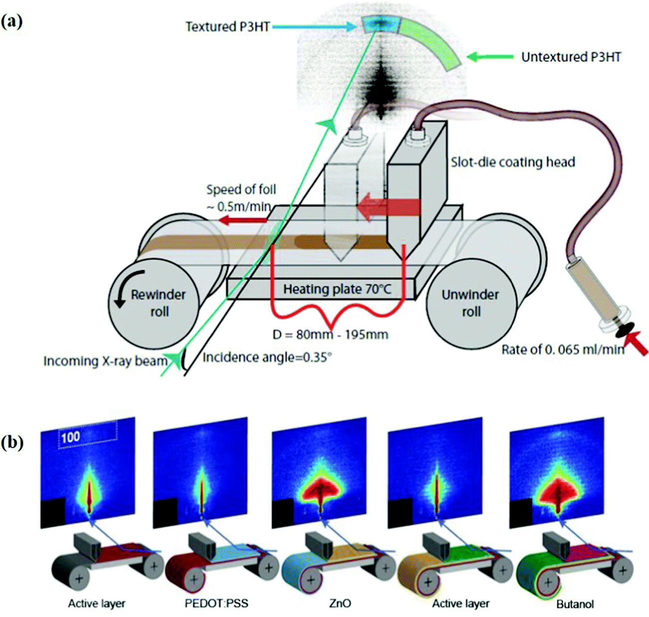 | ||
| Fig. 9 (a) An X-ray set-up where the slot-die coater unit is an integrated part of the small angle X-ray scattering instrument measurements. Adapted with permission.95 Copyright 2014, the authors, under the Creative Commons Attribution 3.0 Unported license. (b) An in situ R2R X-ray scattering measurement used for tandem OSCs. Adapted with permission.96 Copyright 2015, Wiley-VCH Verlag GmbH & Co. KGaA. | ||
The third stage is the large-scale R2R machine production line. It generally has typical web widths over 300 mm. The speed range is wide to allow a long drying time at a low drying speed. A series of processing units are assembled in an inline configuration, including an unwinding and in-feeding system unit, a printing and coating unit, a drying unit (hot air, near-infrared light, lasers, microwaves and intense pulsed light) and an out-feeding and rewinding unit. This large-scale R2R production line is customized by a few companies around the world such as Armor, Eight19, infinityPV, Oxford PV, FOM Technologies and Grafisk Maskinfabrik.
3.2 Module design
Up-scaling high-performance single devices towards high-performance modules is important for large-area device fabrication. As device area increases, the film homogeneity changes, which might induce local defects and decrease the photovoltaic performance of devices. A module is a series of single devices connected and is an effective method to avoid film morphology inhomogeneity during up-scaling. An OSC module is composed of series-connected single devices (Fig. 10) and typically involves three laser ablation processing steps P1, P2 and P3. P1 achieves structuring of the bottom electrode, such as ITO. The P2 scribe goes through the two interfacial layers and active layer until the bottom electrode. Ideal P2 processing achieves a selective ablation of the active layer and interfacial layer without destroying the ITO layer. P3 achieves an isolated top electrode. The main challenge of whole laser patterning is selective ablation of top layers without damaging bottom stacks and decreasing the pattern gap as well. The interconnect patterning parts are incapable of generating photocurrent, which is called the dead area. The GFF is used to describe the effective area of modules, which is defined as the ratio of the active area to the total area of the module: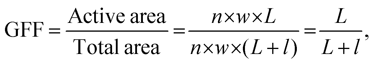 | (7) |
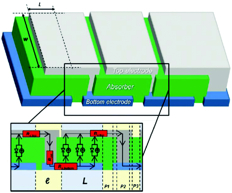 | ||
| Fig. 10 Diagram of module fabrication. Adapted with permission.50 Copyright 2015, Wiley-VCH Verlag GmbH & Co. KGaA. | ||
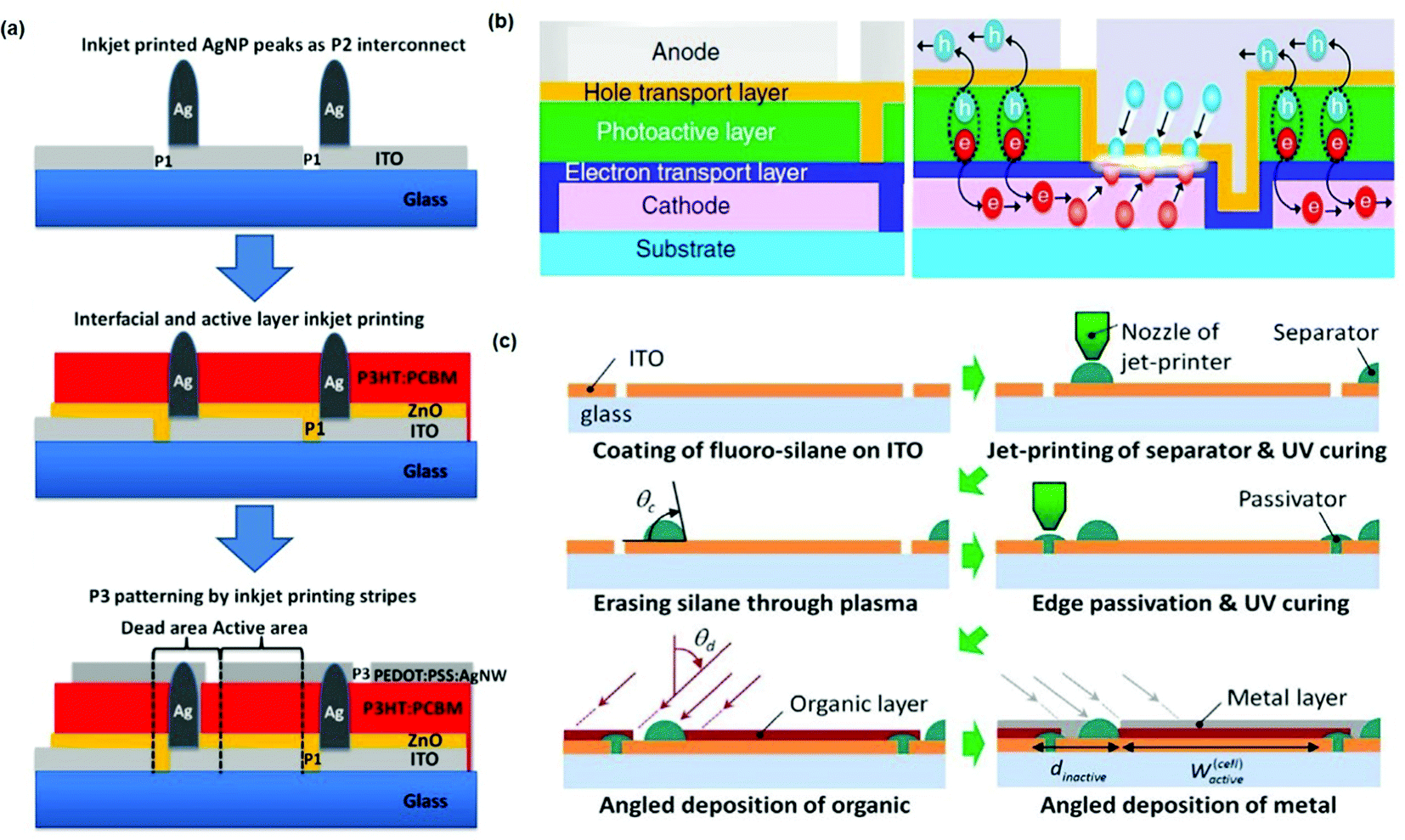
Except for traditional three-step laser patterning, several strategies have been developed to design new modules and achieve effective interconnection. To fabricate “invisible” modules, Egelhaaf et al.107 developed a new strategy to achieve effective but visually inconspicuous interconnects with the combination of inkjet printing (Fig. 11a). In this approach, only top and bottom electrodes were patterned by a laser, and the P2 step was replaced by an Ag bridge. Highly conductive Ag bridges were printed onto the bottom electrodes, forming a conductive pathway to the top electrode. A freedom-shape OSC with 84 cm2 achieved a 1.60% PCE with a high GFF of 95%. Lee et al.108 designed a unique monolithic interconnection that enables efficient module fabrication without patterning the charge transport layers, considering that effective charge recombination occurs at the contacts between charge transport layers (Fig. 11b). By printing the ZnO and MoO3 transport layers with a doctor-blade machine for non-patterned single-layer forms, and printing the active layer and Ag electrode with a slot-die machine for stripe patterning, they fabricated a 4.5 cm2 module with a GFF of 90%. Yoo et al.109 proposed a novel series-connected OSC module fabrication method (Fig. 11c). They designed some linear microstructures by printing a high-viscosity resin. These linear structures exhibited high-angle contact, which can form a separator/interconnect for series-connection devices. This novel module structure exhibited an extremely high GFF of 95.6%.
 | ||
| Fig. 11 (a) Schematic illustration of an OSC module fabricated by the inkjet printing method with hidden interconnects. Adapted with permission.107 Copyright 2018, Wiley-VCH Verlag GmbH & Co. KGaA. (b) A special monolithic interconnection that enables efficient module fabrication without patterning the charge transport layers. Adapted with permission.108 Copyright 2016, the authors, Creative Commons Attribution 4.0 International License. (c) Schematic illustration of a special OSC module design with addition of fluoro-silane. Adapted with permission.109 Copyright 2014, Elsevier. | ||
Another solution of increasing GFF and achieving next-stage arbitrary shaped OSC modules is adopting some high-resolution, 2D printing methods, such as inkjet printing, screen printing and gravure printing. Arbitrary shaped OSCs have higher requirements in the dimensional accuracy compared with traditional rectangular cells. Inkjet printing, screen printing and gravure printing exhibit drop-on-demand properties and accurate 2D printing, which are beneficial for arbitrary deposition of materials. For example, Groen et al.110 fabricated a fully inkjet-printed 1 cm2 OSC (six layers in total). They also fabricated an OSC in the shape of a Christmas tree, which demonstrates the advantage of freedom of design for the inkjet printing. Krebs et al.42 fabricated a “Solar hat” module by screen printing. Sauermann et al.111 adopted slot-die coating and screen printing to fabricate a “Solar Tree”, displayed during the Milan EXPO 2015. Välimäki et al.112 adopted gravure and rotary screen printing methods to fabricate a first “Solar Tree leaf”, achieving the fabrication of arbitrary-shaped OSC modules.
4. Device component processing
The key components of OSCs are the active layer, the interfacial layer, and the electrodes, and all of them have specific requirements for fabricating high-performance large-area devices. Inks of each layer need to be adjusted to meet different requirements during processing. In this part, we will discuss the requirements and process optimization strategy of the printable active layer, interfacial layers and electrodes.4.1 Active layer
For small-area devices, the wet active layer film is dried due to the centrifugal effect during spin coating. However, the film forming and drying behavior in other coating or printing methods is different. Considering that the traditional film morphology optimization strategy may not be adaptable for large-area device fabrication, it is of great importance to seek film optimization strategies for large-area device fabrication. At the same time, in the past decade, many efforts were focused on fabricating large-scale devices or modules based on fullerene acceptors. There are very limited studies focusing on non-fullerene acceptor based OSCs in upscaling printed devices or modules. Considering that non-fullerene acceptors exhibit different packing and aggregation behaviors compared to fullerene acceptors in large-area device printing processes, it is a challenge to find new strategies to optimize non-fullerene-based large-area OSCs. All the mentioned donor polymers and non-fullerene acceptors are shown in Fig. 12 and 13. Table 2 summarizes the printed non-fullerene OSCs discussed in this review. The efficiencies of large-area OSCs are summarized in Fig. 14.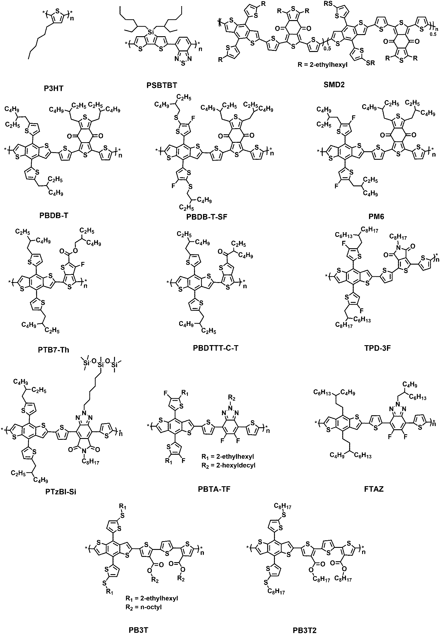 | ||
| Fig. 12 Chemical structures of polymer donors involved in this article. | ||
 | ||
| Fig. 13 Chemical structures of non-fullerene acceptors involved in this article. | ||
| Active layer (deposition method) | Bottom electrode (deposition method) | Top electrode (deposition method) | Area (cm2) | V OC (V) | J SC (mA cm−2) | FF (%) | PCE (%) (average) | Ref. |
|---|---|---|---|---|---|---|---|---|
| PBDB-T-SF:IT-4F (slot-die coating) | Glass/ITO (magnetron sputtering) | Al (thermal evap.) | 0.10 | 0.88 | 20.6 | 71.7 | 13.0 (12.1) | 73 |
| PM6:Y6:PC61BM (blade coating) | Glass/ITO (magnetron sputtering) | Ag (thermal evap.) | 26.2 | 9.82 | 1.75 | 73.5 | 12.6 (12.6) | 106 |
| 204.0 | 26.7 | 0.65 | 69.0 | 12.0 (11.7) | ||||
| PTB7-Th:FOIC (spray coating) | Glass/ITO (magnetron sputtering) | Al (thermal evap.) | 0.05 | 0.70 | 21.7 | 62.0 | 9.45 (9.25) | 115 |
| PBTA-TF:IT-M (blade coating) | Glass/ITO (magnetron sputtering) | Al (thermal evap.) | 1.00 | 0.95 | 17.1 | 65.0 | 10.6 (—) | 116 |
| PBDB-T:ITIC (blade coating) | Glass/ITO (magnetron sputtering) | Al (thermal evap.) | 0.90 | 0.87 | 16.8 | 59.0 | 8.59 (—) | 117 |
| PBDB-T-SF:IT-4F (slot-die coating) | Glass/ITO (magnetron sputtering) | Al (thermal evap.) | 6.25 | 0.87 | 19.5 | 52.0 | 8.95 (7.9) | 118 |
| PBDB-T:ITIC (blade coating) | Glass/ITO (magnetron sputtering) | Al (thermal evap.) | 1.00 | 0.89 | 17.1 | 66.1 | — (10.0) | 119 |
| FTAZ:IT-M (blade coating) | Glass/ITO (magnetron sputtering) | Al (thermal evap.) | 0.07 | 0.95 | 16.8 | 66.1 | 11.0 (10.5) | 120 |
| 0.56 | 0.93 | 16.4 | 64.6 | 9.85 (—) | ||||
| PBDB-T:ITIC (slot-die coating) | Glass/ITO (magnetron sputtering) | Ag (thermal evap.) | 0.10 | 0.88 | 17.5 | 64.9 | 10.0 (9.76) | 121 |
| PET/ITO (magnetron sputtering) | 0.10 | 0.88 | 17.0 | 58.6 | 8.77 (—) | |||
| PM6:Y6 (slot-die coating) | Glass/ITO (magnetron sputtering) | Al (thermal evap.) | 0.56 | 0.80 | 26.4 | 64.2 | 13.8 (13.6) | 122 |
| PM6:IT-4F (blade coating) | Glass/ITO (magnetron sputtering) | Al (thermal evap.) | 0.56 | 0.83 | 19.3 | 67.6 | 11.4 (10.8) | 123 |
| P3HT:o-IDTBR (inkjet printing) | Glass/ITO (magnetron sputtering) | Ag (thermal evap.) | 0.10 | 0.71 | 13.8 | 67.2 | 6.47 (6.11) | 124 |
| 2.20 | 0.72 | 14.1 | 47.0 | 4.76 (—) | ||||
| PBDB-T:ITIC (slot-die coating) | PET/ITO (magnetron sputtering) | Ag (thermal evap.) | 1.04 | 0.86 | 17.0 | 65.2 | 9.77 (9.52) | 125 |
| 15.0 | 5.10 | 2.79 | 60.6 | 8.90 (8.64) | ||||
| PM6:IT-4F (blade coating) | Glass/ITO (magnetron sputtering) | Al (thermal evap.) | 0.12 | 0.86 | 20.8 | 72.0 | 12.88 (12.34) | 126 |
| PM6:Y6 (spin coating) | Glass/ITO (magnetron sputtering) | Al (thermal evap.) | 1.00 | 0.81 | 24.9 | 63.0 | — (12.7) | 129 |
| PM6:IT-4F (blade coating) | Glass/ITO (magnetron sputtering) | Al (thermal evap.) | 1.00 | 0.86 | 21.1 | 72.0 | 13.2 (12.3) | 130 |
| PB3T:IT-M (spin coating) | Glass/ITO (magnetron sputtering) | Al (thermal evap.) | 1.00 | 0.98 | 15.6 | 66.0 | 10.1 (—) | 131 |
| PB3T2:IT-M (spin coating) | Glass/ITO (magnetron sputtering) | Al (thermal evap.) | 0.04 | 0.94 | 17.8 | 63.0 | 10.6 (10.3) | 132 |
| PBDB-T:IT-M (blade coating) | Glass/ITO (magnetron sputtering) | Al (thermal evap.) | 1.00 | 0.91 | 15.5 | 68.0 | 9.67 (—) | 133 |
| PM6:Y6 (spin coating) | Graphene&AgNWs/PH1000 (—) | Al (thermal evap.) | 0.04 | 0.83 | 23.2 | 70.0 | 13.4 (13.2) | 138 |
| PBDB-T:IT-M (spin coating) | PET/PEDOT:PSS (drop casting) | Al (thermal evap.) | 0.04 | 0.925 | 15.6 | 70.7 | 10.2 (10.1) | 143 |
| PTB7-Th:ITIC (blade coating) | Glass/ITO (magnetron sputtering) | Ag (thermal evap.) | 0.14 | 0.83 | 16.0 | 71.0 | 9.54 (9.33) | 144 |
| PET/Ag/TiOx (thermal evap.) | PEDOT:PSS (spin coating) | 2.03 | 0.81 | 14.7 | 63.0 | 7.60 (7.32) | ||
| PM6:Y6 (spin coating) | PET/Em-Ag/AgNWs/AZO (spin coating) | Al (thermal evap.) | 1.00 | 0.80 | 25.0 | 61.0 | 12.3 (—) | 149 |
| TPD-3F:IT-4F (blade coating) | Glass/ITO (magnetron sputtering) | Ag (thermal evap.) | 20.4 | 4.45 | 3.9 | 60.5 | 10.4 (—) | 151 |
| PTB7-Th:COi8DFIC:PC71BM (slot-die coating) | PET/Ag grid/PH1000 (slot-die coating) | Ag (thermal evap.) | 1.0 | 0.69 | 26.7 | 65.8 | 12.2 (12.0) | 152 |
| 25.0 | 3.46 | 4.93 | 59.1 | 10.1 (9.81) | ||||
| 50.0 | 6.85 | 2.54 | 51.9 | 9.05 (8.80) | ||||
| PM6:Y6:PC71BM (spin coating) | PET/Ag grid/AgNWs:PEI-Zn (blade coating) | Ag (thermal evap.) | 10.1 | 0.81 | 23.56 | 66.0 | 12.6 (11.6) | 153 |
| 54.0 | 7.34 | 2.57 | 70.0 | 13.2 (—) | ||||
| PBDB-T:ITIC:PC71BM (blade coating) | Glass/ITO (magnetron sputtering) | Al (thermal evap.) | 216.0 | 14.2 | 0.91 | 59.0 | 7.69 (7.15) | 154 |
| PTzBI-Si:N2200 (slot-die coating) | Glass/ITO (magnetron sputtering) | Ag (thermal evap.) | 1.00 | 0.87 | 16.1 | 72.7 | 10.15 (9.48) | 162 |
| PM6:IT-4F (blade coating) | Glass/ITO (magnetron sputtering) | Ag (thermal evap.) | 1.00 | 0.84 | 20.0 | 68.0 | 11.4 (11.0) | 163 |
| PM6:DTY6 (blade coating) | Glass/ITO (magnetron sputtering) | Ag (thermal evap.) | 18.0 | 5.11 | 3.89 | 72.5 | 14.4 (13.7) | 164 |
| PTB7-Th:EH-IDTBR:T2-OEHRH (blade coating) | Glass/ITO (magnetron sputtering) | Ag (thermal evap.) | 55.5 | 11.47 | 1.29 | 63.0 | 9.32 (—) | 165 |
| SMD2:ITIC-Th (slot-die coating) | PET/ITO (magnetron sputtering) | Ag (screen printing) | 80.0 | 8.80 | 1.12 | 53.1 | 5.25 (—) | 44 |
PBTZT-stat-BDTT-8![[thin space (1/6-em)]](https://www.rsc.org/images/entities/char_2009.gif) :4TICO (blade coating) :4TICO (blade coating) |
Glass/ITO (magnetron sputtering) | PH1000 (blade coating) | 1.10 | 2.89 | 2.95 | 45.7 | 3.9 (3.8) | 101 |
| PSBTBT:PDI-DTT (slot-die coating) | PET/ITO (magnetron sputtering) | Ag (flexo-bed screen printing) | 4.20 | 0.37 | 1.92 | 28.9 | 0.20 (—) | 155 |
| P3HT:o-IDTBR (blade coating) | Glass/ITO (magnetron sputtering) | AgNWs (blade coating) | 0.10 | 0.70 | 11.3 | 66.6 | — (5.25) | 156 |
| 59.5 | 0.69 | 10.9 | 61.9 | 4.7 (4.5) | ||||
| PBDTTT-C-T:PDI-DTT (slot-die coating) | PET/Ag grid/PEDOT:PSS (flexographic, R2R) | Ag grid (flexographic, R2R) | 1.00 | 0.63 | 2.5 | 42.5 | 0.73 (0.67) | 157 |
| PBDTTT-C-T:DC-IDT2T (slot-die coating) | PET/Ag grid/PEDOT:PSS (flexographic, R2R) | Ag (flexographic, R2R) | 1.00 | 0.80 | 3.1 | 40.1 | 1.02 (1.00) | 158 |
| PTB7-Th:IEIC (slot-die coating) | PET/ITO (magnetron sputtering) | Ag (flexographic, R2R) | 0.70 | 0.90 | 5.4 | 36.7 | 2.26 (2.05) | 159 |
| PET/Ag grid/PEDOT:PSS (flexographic, R2R) | 1.00 | 0.94 | 6.9 | 35.2 | 1.79 (1.60) | |||
| PBDB-T:ITIC (slot-die coating) | PET/Ag (magnetron sputtering) | CPP PEDOT (slot-die coating) | 7.14 | 0.86 | 12.0 | 49.0 | 5.5 (5.1) | 169 |
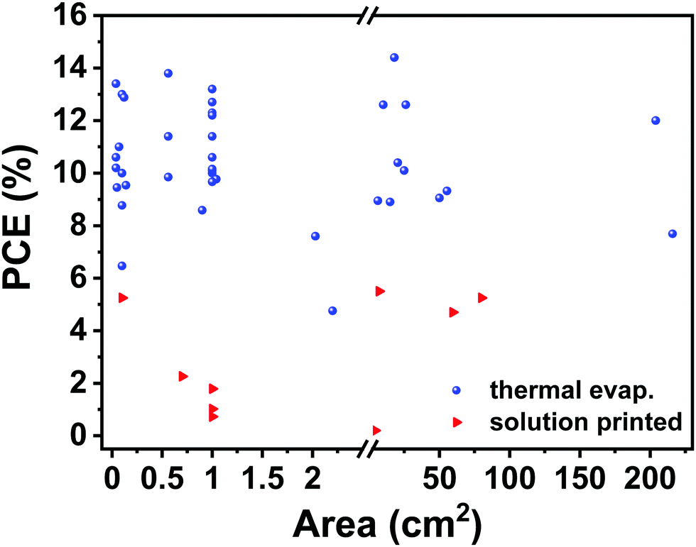 | ||
| Fig. 14 Trend of PCEs with different areas of OSCs. The blue points represent the devices with thermally evaporated top electrodes and the red points represent the devices with solution printed top electrodes. | ||
Solvent engineering is an important strategy to adjust ink rheological properties and optimize the film morphology of large-area devices or modules. The fluidic properties of inks have a great influence on uniform film formation. For example, in inkjet printing, a printable fluid should have a dimensionless Fromm number Z value between 4 and 14 by considering characteristics such as single droplet formability, positional accuracy, and maximum allowable jetting frequency. Z is defined as follows:
 | (8) |
An effective method to adjust the ink rheological properties based on solvent engineering strategies is the use of cosolvents. A cosolvent can effectively control the ink behavior and eliminate the “coffee ring” formation. Generally, the cosolvent is composed of two solvents with different boiling points. By adding a high boiling point solvent, there is a concentration gradient formed at the droplet surface. The counterclockwise Marangoni flow with an opposite movement direction towards the flow direction can prevent the particle segregation. Deng et al.115 fabricated a PTB7-Th:FOIC-based electrospray-deposited OSC, which exhibited a PCE of 9.45%. The low-vapor-pressure non-halogen solvent o-xylene and the high-vapor-pressure solvent chloroform were employed to form a binary solvent system with an ideal evaporation speed, electrical conductivity and sufficient solubility. A longer droplet evaporation time with sufficient solubility can decrease the roughness and domain size of polymer/non-fullerene blend films. Hou et al.116 fabricated PBTA-TF:IT-M-based devices processed with environmentally friendly cosolvents (tetrahydrofuran/isopropyl alcohol). A PCE of 11.7% was achieved by adopting the blade-coating method; for a larger area device with an area of 1.0 cm2, a PCE of 10.6% was still maintained.
An effective method to optimize the morphology of large-area OSCs is using proper additive reagents. Additives usually have different solubilities for the donor and acceptor, so donor/acceptor crystallinity and packing behavior can be optimized during film formation. For large-area printing processes, selecting proper additives is important. For example, Yuan et al.117 investigated the influence of three additives, 1,8-diiodooctane (DIO), 1,8-octanedithiol (ODT) and 1-chloronaphthalene (CN), on the morphology of blade-coated PBDB-T:ITIC devices. Generally, DIO and CN are more beneficial and widely used in spin-coated devices. However, in the blade-coated device (4 mm2), the ODT-based device not only exhibited the best performance with a PCE of 10.2% but also the best device stability. The ODT-based device yielded a slower degradation with retaining 77% of the initial PCE after 150 min light illumination than the DIO-based device (55%). In addition, the ODT-based large-area device (90 mm2) exhibited a high PCE of 8.59%. Apart from additive types, the additive amount needs to be adjusted in large-area printed technologies, which is different from the amounts in lab-scale small-area spin coating technology. For example, slot-die printed OSCs with a device area of 6.25 cm2 based on PBDB-T-SF:IT-4F as the active layer were fabricated with different amounts of DIO. The addition of 0.25 vol% DIO enhanced the average PCE from 3.5% to 7.9%, whereas at lower or higher DIO contents this positive effect is less pronounced.118 The optimized additive amounts in active layers by spin coating (0.5 vol% DIO) and slot-die coating (0.25 vol% DIO) are different owing to differences in the rheological properties of inks, residual solvent amount and solvent volatilization kinetics. Ma et al.119 fabricated devices based on PBDB-T:ITIC by spin coating and blade coating with various DIO contents in air. A high average PCE of 10.03% was achieved for blade-coated devices with 0.25% DIO, higher than that of spin-coated devices with 1% DIO. The deviation in optimum DIO content in printed devices compared with spin-coated devices originates from the different active layer morphologies. The blade coating was found to induce crystal propagation along the direction of shearing. As a result, the partial role of DIO can be replaced by the blade coating technology, which decreases the DIO content in printed devices. In some cases, the additive amount in printed devices can be decreased even to 0%, which is beneficial for improving the device storage lifetime. Ade et al.120 reported a non-fullerene OSC based on blade-coated FTAZ:IT-M as the active layer, and the active layer was processed under air conditions without solvent additives. This FTAZ:IT-M-based device yielded a PCE of nearly 11%. What is more, the storage stability of the device was improved, and this blade-coated FTAZ:IT-M device exhibited negligible performance loss after 20 days of aging in air.
Adjusting the temperature of the ink and substrate is another strategy to obtain uniform films and optimized morphology. Vak et al.121 used a hot slot-die coating method (hot substrate of 120 °C and hot solution of 90 °C) to achieve high-performance ITIC-based 0.1 cm2 devices. For slot-die coating, it is easy to accurately adjust the temperature of the slot-head (ink temperature) and the substrate towards a controlled thermodynamic state of the solution during the film formation. Through heating the slot-die head and substrate, the π–π stacking (010) distance decreased from 3.82 Å (ink temperature: 25 °C/substrate temperature: 25 °C) to 3.68 Å (90 °C/120 °C), leading to enhanced intermolecular interactions and charge transport. Using PEIE as an additional electron injection layer, a PCE of 10.0% was achieved, and PCEs of 8.8% and 7.1% were obtained via flexible substrate batching and roll-to-roll processing, respectively.
An active layer consisting of PM6 and Y6 received considerable attention recently. However, the temperature-dependent polymer PM6 has strong aggregation in widely-used high boiling solvents, e.g. chlorobenzene and 1,2-dichlorobenzene, and some hydrocarbon solvents, e.g. o-xylene and 1,2,4-trimethylbenzene, which limits upscaling. The hot temperature slot-die coating process can fix this problem. With the combination of a hot solution and a hot substrate, the slot-die coated PM6:Y6-based OSCs exhibited high PCEs of 15.2%, 15.4% and 15.6% processed by chlorobenzene, o-xylene and 1,2,4-trimethylbenzene, respectively. Large-area (56 mm2) devices also exhibited high PCEs of 13.9%, 13.7% and 13.9% processed by chlorobenzene, o-xylene and 1,2,4-trimethylbenzene, respectively.122
Adjusting substrate temperature is also important for blade coating. For example, Ma et al.123 varied the substrate temperature in blade-coated PM6:IT-4F devices to control the molecular ordering and phase separation (Fig. 15). The blade-coated devices with a low substrate temperature (30 °C) suffered from the low crystallinity of IT-4F and poor device performance. Through increasing the substrate temperature to 50 °C, a high PCE of 13.64% was achieved in air without any other processing treatments. Through grazing incidence wide angle X-ray scattering (GIWAXS) analysis, no scattering peaks of IT-4F at the low q location was observed in spin coating and blade-coating (30 °C) films, indicating the low crystallinity of IT-4F in these two blend films. A pronounced scattering peak was observed in the in-plane direction at q = 0.31 Å−1 for blade-coating (50 °C) films, which is attributed to IT-4F backbone packing. For spin coating and blade-coating (30 °C) films, IT-4F molecules moved slowly, which results in weak crystallinity. With increasing temperature, molecular movement and arrangement of IT-4F had been triggered, resulting in the thermodynamic intermediate state of backbone packing. The charge transport along the backbone packing is fast, which is beneficial for PCE enhancement.
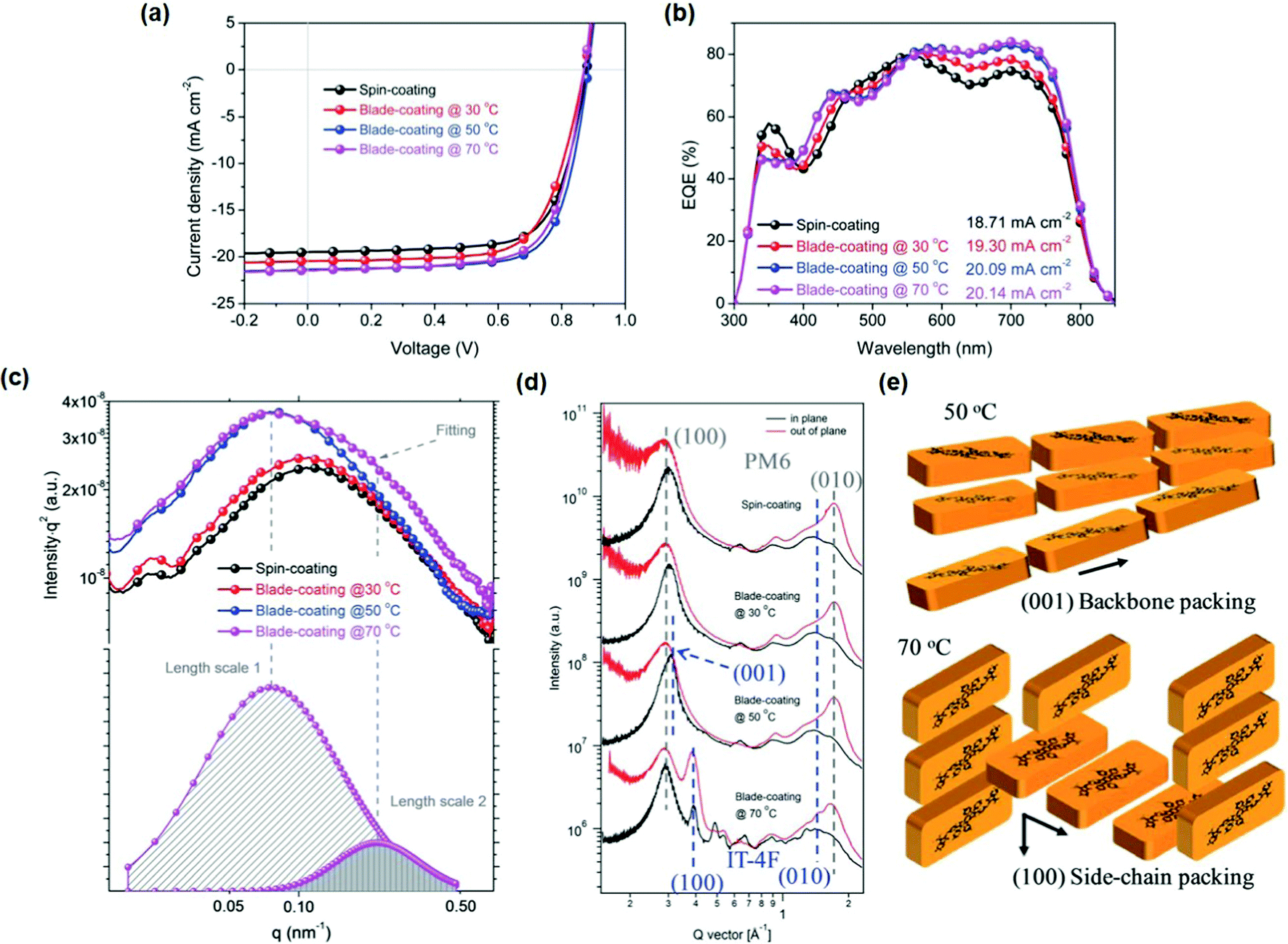 | ||
| Fig. 15 (a) J–V curves, (b) EQE curves, (c) RSoXS profiles, and (d) GIWAXS line profiles of PM6:IT-4F devices based on spin coating and blade coating at 30, 50 and 70 °C. (e) The schematics of molecular packing for IT-4F molecules in the blend films prepared by blade-coating at 50 and 70 °C. Adapted with permission.123 Copyright 2019, The Royal Society of Chemistry. | ||
Adjusting substrate temperature also plays an important role in inkjet printing. For example, Baran et al.124 reported a 0.1 cm2 non-fullerene-based OSC via inkjet printing (Fig. 16). The device efficiency of the P3HT:o-IDTBR device by inkjet printing was 6.47%, comparable to that of spin coating. Furthermore, a 2.2 cm2 turtle-shaped inkjet-printed device achieved a PCE of 4.76%. Through optimizing deposition temperature and drop spacing, common inkjet printing complications like nozzle clogging can be avoided. Fig. 16e presents the influence of deposition temperature and drop spacing on the homogeneity of active layer films. With increasing deposition temperature (>50 °C) and drop spacing (>15 μm), peaks and valleys can be clearly observed, which seriously decreased the device performance.
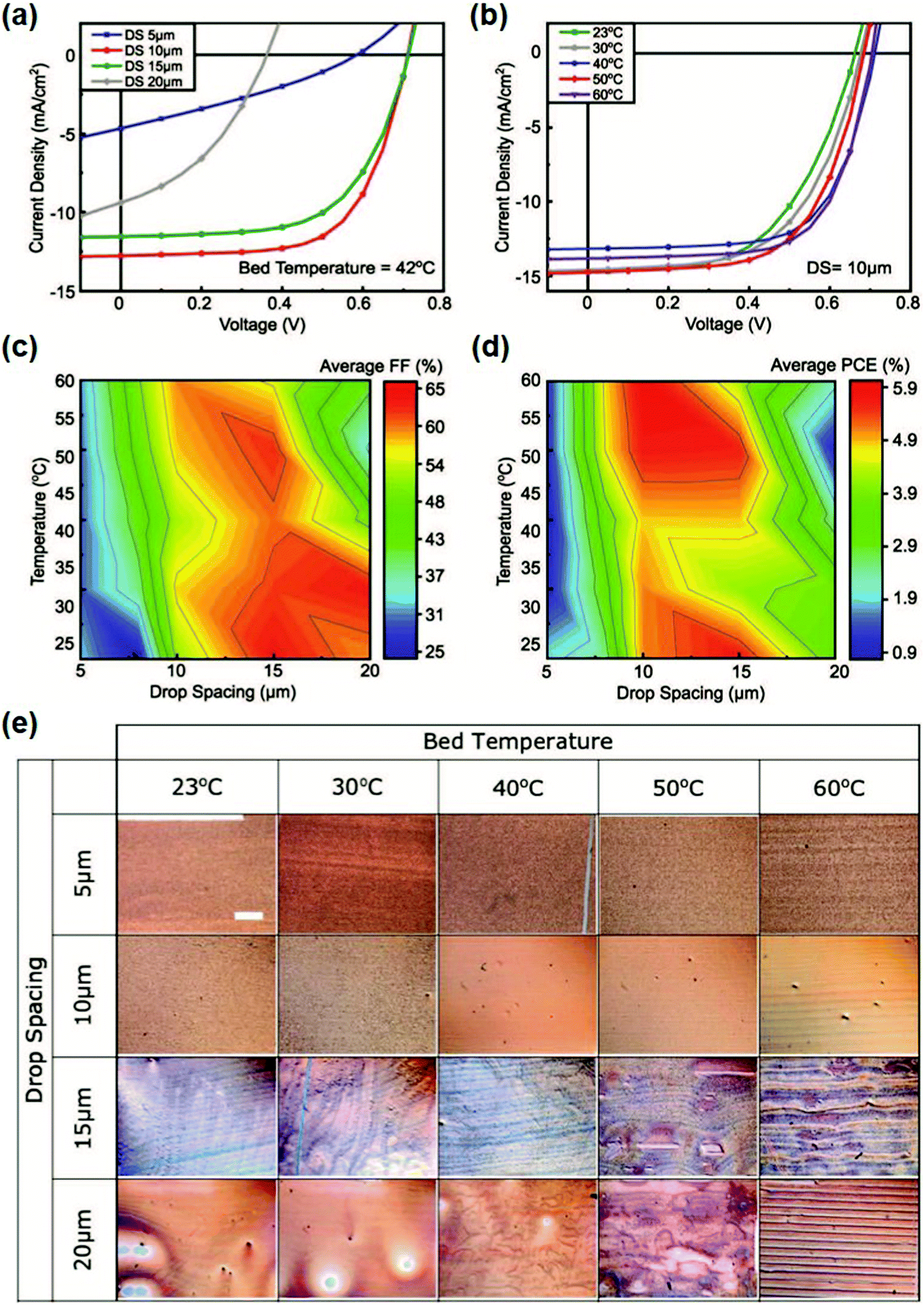 | ||
| Fig. 16 (a) J–V curves of cells inkjet-printed at different drop spacing values at a constant bed temperature of 42 °C. (b) J–V curves of cells inkjet-printed with a fixed drop spacing of 10 μm and changing bed temperature. (c) and (d) Performance maps showing the average fill factor (FF) and PCEs of films inkjet-printed at varying drop spacing and bed temperature values. (e) Optical microscope images displaying the effects of drop spacing and bed temperature for deposition on the homogeneity and uniformity of P3HT:o-IDTBR films (scale bar = 500 μm). Adapted with permission.124 Copyright 2019, Wiley-VCH Verlag GmbH & Co. KGaA. | ||
Adjusting the printing speed is another strategy to obtain a homogeneous film and optimized morphology. Chen et al.125 investigated the relationship between the inking ratio and film morphological evolution in the slot-die coating active layer. The ratio of inking speed (0.10–0.20 mL min−1) to stripping speed (0.10–0.15 m min−1) is defined as the inking ratio, which describes the actual volume of ink printed per unit area. Excessive aggregation occurred in both low or high inking ratio-based films. Based on the device structure of PET/ITO/PBDB-T:ITIC/MoO3/Ag, the PCE of this 1.04 cm2 flexible device was 9.77%, and the PCE of the 15 cm2 flexible device can still maintain 91% compared with the 1.04 cm2 flexible device.
4.2 Interfacial layer
In order to promote large-area fab-scale OSC fabrication, all functional layers should be processed in scalable production technologies. High-quality printable interfacial layers with excellent thickness tolerance are important for large-area OSC fabrication. Generally, the active layer thickness is 100–300 nm, the interfacial layer thickness is 20–50 nm and the electrode thickness is 100–1000 nm. Considering the low thickness of the interfacial layer, a slight thickness variation may lead to significant performance deterioration. Thus, an ideal interfacial layer should meet the following requirements: high thickness tolerance, ultrahigh transparency in visible and near-infrared light regions, high electrical conductivity, superior charge carrier collection and transport properties, excellent chemical, thermal and photo-stability, suitable energy levels and low interfacial trap density.As the cathode interfacial layer, ZnO is widely used owing to its high electron mobility, high visible light transparency and high thermal stability. The thickness and morphology of ZnO layers show great influence on the performance of printed devices. Ma et al.126 investigated the influence of the surface morphology of ZnO interfacial layers on the performance of inverted OSCs with spin-coated and blade-coated active layers. The ZnO surface roughness exhibited a negligible influence on the optimized performance, performance uniformity and long-term stability of the spin-coated OSCs. However, the ZnO surface roughness significantly affected the performance and stability of the blade-coated devices. Compared with centrifugal forces in the spin coating method, the shear force in the blade-coating method is milder and the molecules had the tendency to precipitate during the slow drying process. The ZnO rough surface accelerated the precipitation process, leading to a poor contact between the interfacial layer and active layer. By using methanol-based ink to replace the acetone-based one, a smoother ZnO layer can be achieved; higher PCEs of 12.88% and 9.22% were achieved for the 0.12 and 1.04 cm2 doctor-bladed PM6:IT-4F OSCs. By sensitizing ZnO nanocrystals with a conjugated polymer (poly(9,9-bis-(6′-diethoxyphosphorylhexyl)fluorene) (PFEP)), Zhang et al.127 fabricated a printable highly conductive cathode interfacial layer. PFEP has dual effects. On one hand, PFEP polymer chains can assemble on ZnO surfaces via their pending phosphonate groups, leading to the formation of a uniform and smooth film during solution processing; on the other hand, charge transfer can occur between ZnO and PFEP, which improves the conductivity of the interfacial layer. By blade coating, a PCE of 6.26% was achieved in P(IID-DTC):PC71BM-based OSCs with a device area of 12.5 mm2. To fabricate large-area (1 cm2) inverted OSCs via R2R micro-gravure printing, a composite ink of ZnO and polyethylenimine (PEI) was developed.128 Modification of ZnO nanoparticles by PEI effectively improved the ink stability and mechanical properties. A PCE of 6% was obtained for the flexible device based on a PTB7-Th:PC71BM active layer with a thick R2R printed ZnO:PEI interfacial layer (∼120 nm).
In addition to ZnO, some other metal oxides also exhibit good thickness tolerance. For example, Tan et al.129 reported a chemically precipitated SnO2 nanoparticle as the cathode interfacial layer, which exhibited excellent thickness tolerance. When the thickness of blade-coated SnO2 layers is up to 530 nm, the PCE of PM6:Y6-based 4 mm2 OSCs remained 12.08%, just slightly lower than that for the 40 nm-SnO2 counterpart (14.45%). For large-area OSCs (100 mm2 area) with a blade-coated 100 nm-thick SnO2 layer, the PCE reached 12.7%.
Some n-doped organic semiconductors based on perylene diimide and naphthalene diimide also exhibit good thickness tolerance. For example, Hou et al.130 used (N,N-dimethylamino)propyl naphthalene diimide (NDI-N) as a printable cathode interfacial layer. Based on the device structure of ITO/PEDOT:PSS/PM6:IT-4F/NDI-N/Ag, a large-area OSC device (1 cm2) was fabricated with a blade-coated NDI-N layer. Compared with ZnO nanoparticle and PFN-Br interfacial layers, blade-coated NDI-N layers exhibited a smoother and more uniform surface, better wetting properties on the active layer surface and a greater thickness tolerance; a PCE of 13.2% was achieved.
Compared with the active layer and cathode interfacial layer, the anode interfacial layer generally exhibits poor thickness tolerance, which impedes the realization of large-area printed OSCs with high efficiency. A doping strategy is usually used to improve the charge transport properties and thickness tolerance of interfacial layers. An n-doped molybdenum oxide anode interfacial layer, which is an aqueous solution of ammonium heptamolybdate precursor with ethylene glycol, was reported by Hou et al.131 With this ethylene glycol-based molybdenum oxide as the anode interfacial layer (ca. 10 nm), OSCs based on PB3T:IT-M exhibited PCEs of 12.1% (spin coating), 11.9% (wire-bar coating) and 11.5% (blade-coating). The device performance was insensitive to the anode interfacial layer thickness variation. When the thickness of the anode interfacial layer increased to 60 nm, the OSC still exhibited a PCE over 11%. In addition, 1 cm2 area devices with a wire-bar coated anode interfacial layer also exhibited a high PCE of 10.1%. By adding vitamin C into ammonium molybdate tetrahydrate, another n-doped MoOx (H:V-Mo) can be prepared.132 Compared with pristine MoOx, the conductivity of n-doped MoOx was dramatically improved by four orders of magnitude, from 1.2 × 10⁻⁷ S m−1 to 1.1 × 10⁻³ S m−1. By varying the thickness of the H:V-Mo anode interfacial layer from 10 to 150 nm, the VOC and FF of the devices were almost the same. Based on the device structure of ITO/ZnO/PB3T2:IT-M/bladed H:V-Mo/Al, a PCE of 10.6% was achieved, slightly lower than that of spin-coated H:V-Mo based devices (11.1%).
Doped polyelectrolytes are another kind of anode interfacial layer material. For example, a p-type self-doped conjugated polyelectrolyte, PCP-3B, is a printable anode interfacial layer for large-area OSCs synthesized by Xu et al.133 As a cyclopentadithiophene-based polymer, PCP-3B shows a high conductivity of 2.85 × 10⁻³ S m−1, comparable to that of the traditional MoOx interfacial material, a high work function of 5.01 eV, comparable to that of PEDOT:PSS, and good wetting properties on the ITO surface. Based on the PCP-3B anode interfacial layer, a 1 cm2 PBDB-T:IT-M-based all blade-coated device achieved a PCE of 9.67%. PEDOT:PSS is the most common anode interfacial layer in conventional spin-coated OSCs. However, in inverted OSCs, particularly with a large area, the film formation of aqueous PEDOT:PSS on the hydrophobic active layer is a challenge. The mismatch in surface energy causes de-wetting and finally induces the formation of inhomogeneous layers. To solve this problem, surfactants are employed in aqueous PEDOT:PSS solution. Groen et al.134 adopted a combination of alcohol, 1-pentanol and a fluorosurfactant (Capstone FS-3100) as the additive to effectively reduce the surface tension of aqueous PEDOT:PSS, which finally helped to form a homogeneous PEDOT:PSS film on the active layer. This transport layer exhibited good thickness tolerance, where the device performance was almost maintained with the thickness of the PEDOT:PSS layer varying from 50 nm to 400 nm.
4.3 Electrodes
For lab-scale OSCs, ITO is the most widely used transparent electrode. However, considering its brittleness and insufficient abundance, it is considered as a bottleneck for fab-scale device fabrication. Some researchers replaced ITO using carbon-based materials, conducting polymers, metal grids and metal nanowires.Carbon-based materials mainly refer to graphene and carbon nanotubes (CNTs). Graphene and CNTs exhibit unique physical and chemical properties: high optical transparency, high electrical conductivity, good chemical and thermal stability and excellent mechanical flexibility, and are ideal candidates for transparent electrodes.135 For example, Matsuo et al.136 employed single-walled CNTs to fabricate metal-free semi-transparent OSCs. The single-walled CNT film was p-doped using two dopants: HNO3 doped via sandwich transfer and MoO3 doped via bridge transfer. Peng et al.137 demonstrated a continuous R2R production of a transparent conductive flexible film with a structure of PET/ethylene vinyl acetate/silver nanowire/graphene. A large-area graphene film was grown on a Cu foil via a R2R chemical vapor deposition process. Then, this film was hot-laminated onto an Ag nanowire precoated PET film. Afterwards, the Cu foil was reused through a R2R electrochemical delamination process. This transparent electrode exhibited a low sheet resistance of 8 Ω sq−1 with a high transmittance of 94% at 550 nm. Ge et al.138 reported a transparent electrode consisting of graphene, an Ag nanowire and a PH1000 composite. With this graphene/Ag nanowire/PH1000 hybrid electrode, OSCs based on PM6:Y6 exhibited a high PCE of 13.4%. The device retained 84.6% of its initial PCE after bending 1000 times (r = 2 mm), showing excellent mechanical flexibility.
The solution-processed transparent conducting polymer PEDOT:PSS has some advantages: high optical transparency in the visible light region, high work function (ca. 5.0 eV) and low cost, which is beneficial for flexible electrode fabrication. The cost of solution-processed PEDOT:PSS electrodes is less than 1% of that of ITO electrodes.139,140 The conductivity of PEDOT:PSS is improved through doping or post-treatment strategies, while some pristine PEDOT:PSS solution (PEDOT:PSS 4083) exhibits low conductivity, less than 10−3 S cm−1. Some solvents (N,N-dimethylformamide, dimethyl sulfoxide, ethylene glycol, tetrahydrofuran, etc.), surfactants and ionic liquids are used to improve conductivity. Inganäs et al.141 firstly reported doping of glycerol into PEDOT:PSS solution. Kim et al.142 reported that doping dimethyl sulfoxide into PEDOT:PSS solution (PH500) can improve the conductivity from 1 S cm−1 to >500 S cm−1. The conductivity of PEDOT:PSS films can be improved to >2000 S cm−1 by doping strategies. Ge et al.143 dropped PEDOT:PSS aqueous solution (PH1000) onto PET plastic substrates to fabricate flexible electrodes. With dimethyl sulfoxide/methanesulfonic acid treated PEDOT:PSS electrodes, flexible OSCs based on PBDB-T:IT-M active layers displayed a PCE of 10.23%. The PEDOT:PSS layer discussed above can be used not only as the bottom electrode but also as the top electrode. Hou et al.144 reported a spin-coated PEDOT:PSS layer as the top electrode; a PCE of 7.6% was realized in the flexible large-area (2.03 cm2) OSCs with the architecture of Ag/TiOx/PTB7-Th:ITIC/PEDOT:PSS.
Metal grids/meshes and metal nanowires are widely adopted as transparent electrodes owing to their inherent advantages, e.g. easy solution processing, high conductivity, and high transmittance in visible and NIR regions. For metal grids/meshes, post-treatments, e.g. thermal annealing, laser sintering and acid treatments, are widely employed to improve conductivity. For example, Lee et al.145 reported that a post-annealing process of the Ag nanogrid at 170 °C can reduce the average sheet resistance from 250.3 to 15.2 Ω sq−1. Blom et al.146 used an effective photonic sintering process to fabricate printed metal grids in OSCs; the resistivity of Ag grids fabricated by a photonic sintering process for 5 s was similar to the resistivity of those fabricated by oven thermal sintering at 130 °C for 6 h. Silver nanowires (Ag NWs) have attracted great attention due to their excellent conductivity, high transparency and flexibility. They are widely used in hybrid electrode fabrication. For example, Wei et al.147 employed Ag NWs as the bottom electrode, which was deposited on a flexible PET substrate by cross slot-die coating. Compared with ITO electrodes, the conducting PET/cross-coated Ag NW flexible film exhibited a transmittance of 94.9% to 70.8% in the visible range and a high conductivity. A large area (7 cm2) flexible OSC based on PPDT2FBT:PCBM exhibited a PCE of 3.04%. Yu et al.148 fabricated a transparent hybrid electrode: the inkjet-printed Ag grid was combined with Ag NWs. The printed Ag grid fills the gap between the Ag NWs and reduces the sheet resistance of the Ag NW film. The hybrid electrode exhibited a low sheet resistivity of 22.5 Ω sq−1 with a high transmittance of 89% at 550 nm, which is comparable to ITO electrodes. Li et al.149 reported a PET/embedded Ag/Ag NWs/Al-doped ZnO composite flexible electrode. The hybrid electrode exhibited a low sheet resistance of 18 Ω sq−1 with an average transmittance of 84% in the range of 500–1000 nm; the flexible OSCs based on PM6:Y6 exhibited high PCEs of 15.21% (0.04 cm2) and 12.28% (1 cm2), respectively. Direct inkjet printing of a patterned, high-quality Ag NW network is relatively difficult. In order to avoid nozzle congestion, the ink concentration, printing parameters and post-treatment have to be carefully adjusted. For example, Coleman et al.150 developed a well-defined Ag NW pattern by inkjet-printing an optimized isopropyl alcohol-diethylene glycol dispersion. The addition of diethylene glycol into a diluted isopropyl alcohol suspension enabled the ink to be printable without any satellite droplets.
5. Printed devices and modules
5.1 Large-area or flexible printed OSCs
In order to achieve a gradual transfer from small-scale to large-scale OSC fabrication, three stages are involved: (1) vacuum evaporation-assisted stage: the active and transport layers are processed with scalable technologies, such as slot-die coating and inkjet printing, while the top electrodes are still thermally vacuum-evaporated; (2) fully R2R-compatible stage: replacing vacuum evaporated electrodes with a solution-processed alternative, fully R2R-compatible devices or modules are fabricated; (3) ITO-free, R2R processing stage: replacing sputtered ITO front transparent electrodes with a solution-processed transparent electrode, each layer is R2R printed.For the first stage, large-area devices and modules developed rapidly. Facchetti et al.151 used o-xylene as the solvent to fabricate doctor-bladed modules based on TPD-3F:IT-4F, which exhibited a certified PCE of 10.4% for an area of 20.4 cm2. In addition, the same module delivered a PCE of 22% under indoor lighting. Wei et al.152 adopted a honeycomb PET/silver-grid as the electrode with slot-die coating. The PTB7-Th:COi8DFIC:PC71BM active layer was slot-die-coated at a high temperature (80 °C) with o-xylene as the processing solvent. They fabricated a flexible single-cell of 1 cm2 with a high PCE of 12.16%. For modules with areas of 25 and 50 cm2, PCEs of 10.09% and 9.05% were achieved, respectively. Furthermore, this flexible silver-grid OSC exhibited excellent mechanical bending performance. After 1000 bending cycles, the PCE remained at 94% (radius = 5 mm) and 99% (radius = 10 mm) of its initial value (Fig. 17). Zhou et al.153 reported large-area flexible devices with PCEs of 13.1% and 12.6% with areas of 6 and 10 cm2, respectively, and flexible modules with a PCE of 13.2% (54 cm2) based on PET/Ag grid/Ag NW:PEI-Zn/PM6:Y6:PC71BM/MoO3/Ag. The PEI-Zn is beneficial for filling the Ag NW network void spaces, decreasing the surface roughness of the Ag NW film from 10.4 nm to 2.3 nm, and improving the thermal stability. The flexible OSCs almost retained their initial PCE values even after 1000 bending cycles (radius = 4 mm). Zan et al.154 fabricated a 214 cm2 OSC module based on PBDB-T:ITIC:PC71BM, which yielded a PCE of 7.7%. By the blade coating method, a uniform active layer can be formed. This large-area module exhibited good stability, and the PCE was maintained at 86% after 140 days of storage at room temperature, 86% after 35 days of storage at 65 °C and 73% after 30 days of storage at 85 °C.
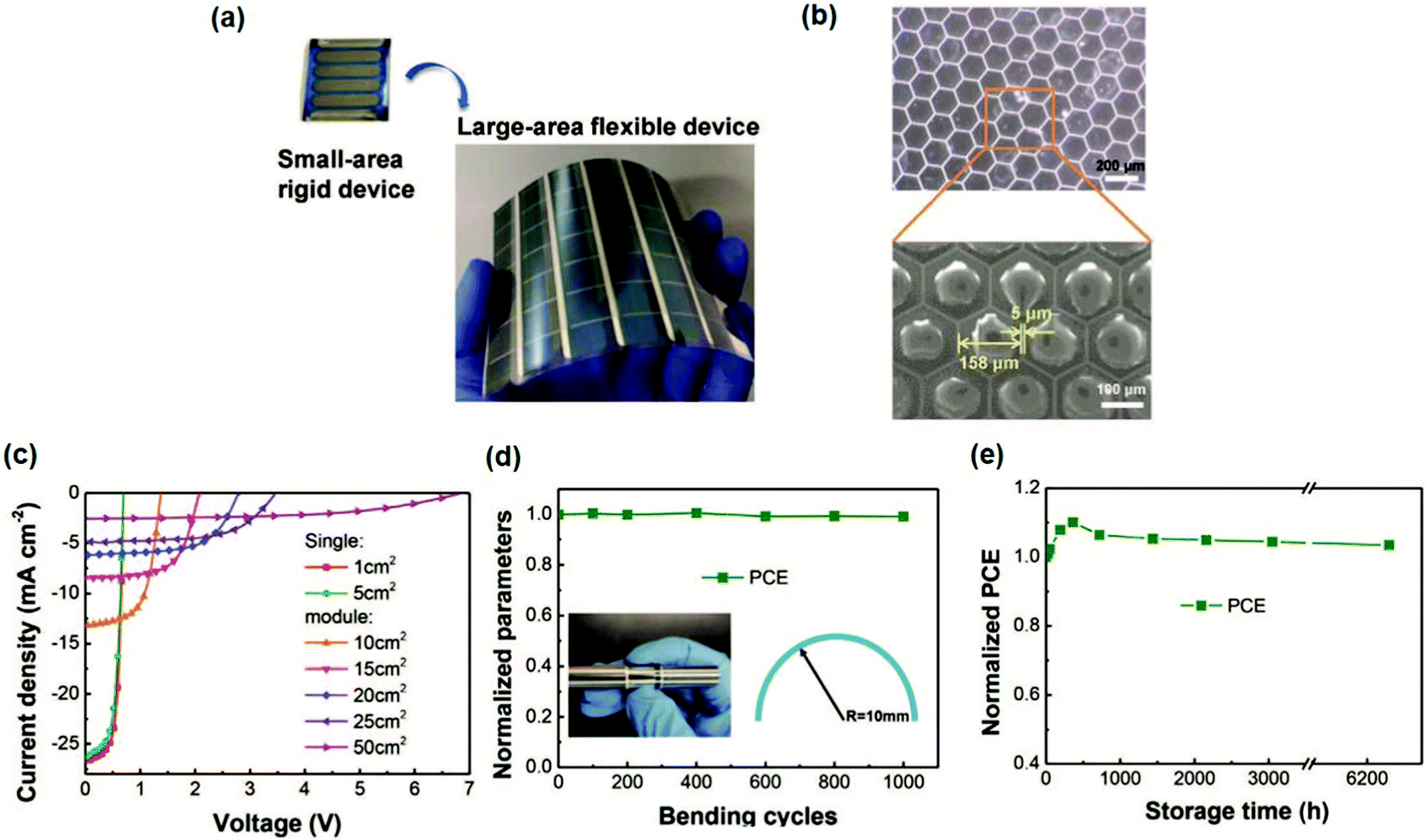 | ||
| Fig. 17 (a) The small area rigid device and large-area flexible device. (b) Optical microscopy and SEM images of the PET/silver-grid substrate. (c) J–V curves of the PTB7-Th:COi8DFIC:PC71BM film coated by the slot-die method with different device areas. (d) Bending stability test. (e) Storage stability of devices in a nitrogen glove box. Adapted with permission.152 Copyright 2020, Wiley-VCH Verlag GmbH & Co. KGaA. | ||
For the second stage, only a few studies on fully-printed, vacuum-free processed non-fullerene OSCs have been reported. The first work was published in 2013 by Zhan et al.155 who reported a large-area inverted all-polymer solar cell by a R2R processing method. The active layer consisted of a PDI-based polymer, PDI-DTT, as the electron acceptor and a dithienosilole-based polymer, PSBTBT, as the electron donor. An inverted structure of ITO/ZnO nanoparticle/active layer/PEDOT:PSS/Ag was used. The ZnO layer, active layer and PEDOT:PSS layer were slot-die-coated, and an Ag back electrode was deposited using a R2R compatible flat-bed screen printing. A 4.2 cm2 large-area module with a PCE of 0.204% was successfully fabricated. In 2018, Brabec et al.156 designed a fully solution-processed R2R compatible module with the device structure of ITO/ZnO nanoparticle/P3HT:o-IDTBR/PEDOT:PSS/Ag NWs. All printed layers were processed using a home-made doctor blading coater. They fabricated a fully-printed small area device (0.104 cm2) with Ag NWs as the top electrode. Furthermore, they upscaled a single cell to a module with a 59.5 cm2 area. The module exhibited a PCE of 4.7%.
Replacing the bottom ITO electrode with solution-processed electrodes is the final stage. In 2014, Zhan et al.157 fabricated a fully R2R processed fullerene-free OSC. The all-polymer solar cells with an inverted device structure of Ag/PEDOT:PSS/ZnO/PBDTTT-C-T:PDI-DTT/PEDOT:PSS/Ag exhibited an average PCE of 0.67% for 1 cm2 devices. In the following year, they reported a fullerene-free large-area printed OSC based on the polymer donor PBDTTT-C-T and the non-fullerene small molecule acceptor DC-IDT2T. A PCE of 1.019% was achieved with a large device area (1 cm2) on flexible substrates. The devices are ITO-free and fabricated under vacuum-free and ambient conditions. This fullerene-free device showed superior stability under continuous AM 1.5G illumination, maintaining more than 80% of their initial efficiency, compared with the fullerene-based device (50%).158 In 2016, Zhan et al.159 reported a fully-printed device based on PTB7-Th:IEIC as the active layer (Fig. 18). They employed two types of flexible device structures on a PET foil: (1) ITO-free, Ag/PEDOT:PSS/ZnO/PTB7-Th:IEIC/PEDOT:PSS/Ag, and (2) ITO, ITO/ZnO/PTB7-Th:IEIC/PEDOT:PSS/Ag. The ITO-free devices were fabricated using flexographic printing for the electrodes and slot-die coating for the other layers. For the ITO-free devices, an average PCE of 1.60% with a champion PCE of 1.79% was obtained for 1 cm2 devices.
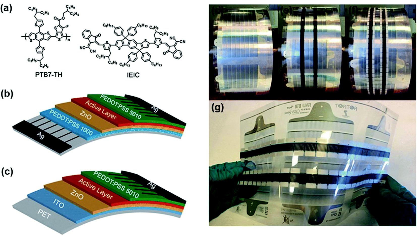 | ||
| Fig. 18 (a) The molecular structures of PTB7-Th and IEIC. The structures of the OSCs based on (b) an ITO-free substrate and (c) a flexible ITO substrate. (d) PEDOT:PSS (PH1000) and ZnO coated PET flexible substrates with an Ag grid (ITO-free substrate). (e) Slot-die coating of the active layer of PTB7-Th:IEIC and PEDOT:PSS interfacial layers. (f) Flexographic printing of the top Ag electrode. (g) Long stripes of roll-coated FREA OSCs based on the ITO-free substrate. Adapted with permission.159 Copyright 2016, The Royal Society of Chemistry. | ||
5.2 Green production
Green production methods, including green synthetic methods and green processing methods, are important for future large-scale OSC fabrication.160,161 The widely used toxic halogenated solvents, e.g. chloroform, chlorobenzene and dichlorobenzene, are incompatible for large-scale industrial production. Adopting halogen-free solvents in fabrication of large-area OSC devices and modules is an emerging topic. Liu et al.162 used 2-methyltetrahydrofuran as the solvent to regulate the morphology of all-polymer devices based on the PTzBI-Si:N2200 active layer. A high PCE of 10.15% was achieved with a 1 cm2 device area. Huang et al.163 reported sequentially blade-coated OSCs based on PM6:Y6. With o-xylene as the solvent, a PCE of 11.4% was obtained for large-area (1 cm2) OSCs. Furthermore, Huang et al.164 reported a large-area module (18 cm2) based on PM6:DTY6 with a high efficiency of 14.4% when processed from o-xylene as the non-halogen solvent. The module retained 89% of the efficiency when the device area was scaled up from 0.04 cm2 (PCE = 16.1%) to 18 cm2. Lee et al.165 fabricated a large-area OSC module (100 cm2 of substrate size, 55.5 cm2 of aperture size) with an encouraging PCE of 9.32% based on PTB7-Th:EH-IDTBR:T2-OEHRH as the active layer. The whole module was processed with toluene as the solvent under air conditions using a D-bar coating. This is one of the highest efficiencies for the NFA-based large-area OSC devices processed from green solvents.5.3 Device encapsulation
The overall market feasibility of organic photovoltaics relies on not only high efficiency, fabrication scalability and environmental friendliness, but also long lifetime. Development of new barrier materials and encapsulation strategies to protect the sensitive active layer from moisture and oxygen ingress is essential for prolonging the lifespan of large-scale OSC devices and modules. Furthermore, barrier materials can block UV irradiation, improve thermal stability, and protect the device from mechanical degradation. Flexible thin glass, flexible polymers, reactive polymer nanocomposites and single/multilayer organic and/or inorganic thin films are emerging flexible barrier materials in encapsulation.166,167In the roll-to-roll fabrication process of printed OSC devices and modules, the final step is roll-to-roll encapsulation. Krebs et al.168 summarized three effective R2R encapsulation lamination strategies, namely UV-curable epoxy resin, hot melting and pressure sensitive adhesives. In fact, no real R2R encapsulation has been performed on flexible non-fullerene-based OSC devices. Madsen et al.169 adopted a combination of R2R vacuum deposition and sheet-to-sheet slot-die coating to fabricate an ITO-free, 7.14 cm2 OSC module based on PET/Ag/ZnO/PBDB-T:ITIC/HTL solar/CPP PEDOT:PSS. The OSC module was encapsulated with two types of flexible barrier films, namely a commercial barrier film (3M Ultra Barrier Films 510) and a new barrier film based on a single 100 nm thick layer of zinc-tin-oxide deposited on a peelable-clean-surface film (Dupont Teijin Films). With the barrier film protection, a long stability under dark conditions over 1000 hours for the OSC module was achieved.
6. Summary and perspective
Large-area OSCs with high PCEs are highly desired for future applications. However, the photovoltaic performance of fab-scale devices still lags behind the lab-scale ones. Coating/printing technology, upscaling equipment and various device component processing strategies are key aspects for upscaling large-area OSCs.Spin coating is the most widely used method in small-area device fabrication, but the high material waste and uncontrollable pattern are not suitable for large-area fabrication. Some large-area printing methods show great potential for upscaling devices, such as spray coating, inkjet printing, blade coating, rotary screen printing, flat-bed screen printing, knife-over-edge coating, slot-die coating, gravure printing and flexographic printing. Blade coating is widely used for active layer printing in fab-scale trials owing to its low cost and easy processing. Slot-die coating and inkjet printing are often used in shape-free devices because of their high resolution and high material utilization. As for metallic electrodes, screen printing and flexographic printing are more proper because these printing technologies are suitable for printing high viscosity inks. In a fully R2R process, various coating/printing technologies are required. By choosing a set of suitable operating parameters (ink velocity, ink volatility, processing parameters, etc.) in different coating/printing technologies, coffee ring, nozzle clogging and satellite droplet formation can be avoided and a high-efficiency R2R process can be carried out.
Lab-to-fab upscaling requires not only advanced fabrication technology, but also the development of equipment and the proper design of modules. At the lab stage, a desktop-based system is usually adopted to test new fabrication technologies. However, this non-integrated lab-scale equipment cannot be directly used in a R2R system. A roll-based system was developed from a single mini roll-coater to a fab-scale R2R system. A relatively complete R2R production line should be composed of a series of processing units, including an unwinding and in-feeding system unit, a printing and coating unit, a drying unit and a rewinding unit. Furthermore, testing and analysis units are also important for a production line to weed out bad products.
Apart from upscaling of fabrication technology and equipment, various device (or module) component processing strategies are also important. Here, the device (or module) component includes the active layer, the interfacial layer and the electrodes. For the active layer, the film forming and drying behaviors are different by using different coating or printing methods in large-area devices. Meanwhile, in large-area printing, non-fullerene acceptors exhibit different packing and aggregation behaviors compared with fullerene acceptors. New strategies to construct high-performance non-fullerene-based large-area OSCs are highly desired. By solvent engineering (including cosolvents, additives, etc.) and other printing parameter engineering strategies (including adjusting ink temperature, substrate temperature, printing speed, etc.), ink properties and film formation can be controlled. For interfacial layers, thickness tolerant cathode/anode interfacial layer materials are desired. The low conductivity and poor wetting properties restrict thicker and smoother interfacial layer printing. Doping, post-treatment and more strategies can effectively fix the abovementioned problems. For electrodes, replacing sputtered ITO bottom electrodes and thermally evaporated top electrodes is the future development direction. Electrodes with high transmittance in visible and NIR regions, low sheet resistance, and easy solution processing, including graphene, carbon nanotubes, PEDOT:PSS, Ag nanowires and Ag nanoparticles, developed rapidly.
The development from lab-scale to fab-scale R2R-processed OSCs involved three stages: (1) vacuum evaporation-assisted stage; (2) fully solution-processed, R2R-compatible stage; and (3) ITO-free, fully R2R stage. There are limited studies on fully-printed, vacuum-free processing of fullerene-free OSCs. For devices or modules with areas larger than 50 cm2, even 100 cm2, they mostly still stay in the vacuum evaporation-assisted stage and had not reached the fully R2R solution processing stage yet. Enlarging device or module areas, maintaining high PCE values and achieving fully R2R solution processing is the future development direction. For the upscaling of OSCs the following issues need to be addressed. Firstly, exploring thickness insensitive active layers and interfacial layers are essential. Non-fullerene acceptors, particularly FREAs, exhibit high exciton diffusion lengths and high electron mobilities, and have a great potential for fabricating thick-film active layers. Designing novel photoactive layer materials with higher mobility or adopting ternary blend strategies is beneficial for fabricating thick active layers. As for interfacial layers, apart from doping strategies, surface passivation can be used to effectively decrease the number of surface defects and improve charge transport properties and interfacial contact between the active layer and the interfacial layer, which may be effective for enhancing the thickness-tolerance of interfacial layers. Secondly, for lab-scale and fab-scale printing/coating technologies, the ink rheology and solvent volatilization behavior are different. A deeper understanding of film forming dynamic processes and physical mechanisms has been acquired. Analyzing physical mechanisms and adopting proper printing process parameters are required to produce homogeneous layers, including the active layer, interfacial layers and electrode layers. Thirdly, in situ morphology testing to weed out bad products is important, while in situ morphology measurements are assembled in lab-trials. The integration of high-speed measurements into a R2R production line is still a challenge. Except for GISAXS measurements, LBIC systems, photoluminescence, electroluminescence imaging and lock-in thermography are being developed to study defects. Fourthly, assembling single cells to a module with a high GFF is essential. Exploring high-resolution and low-cost laser patterning technology is a tendency for achieving a high GFF in large-area OSCs. By combining appropriate printing/coating methods, stable and effective fabrication equipment lines and effective device component processing strategies, high-performance large-area OSCs can be realized in the near future.
Conflicts of interest
The authors declare no conflicts of interest.Acknowledgements
This work was supported by the National Natural Science Foundation of China (21734001 and 51761165023).References
- G. Li, R. Zhu and Y. Yang, Nat. Photonics, 2012, 6, 153–161 CrossRef CAS.
- L. Lu, T. Zheng, Q. Wu, A. M. Schneider, D. Zhao and L. Yu, Chem. Rev., 2015, 115, 12666–12731 CrossRef CAS.
- D. Kearns and M. Calvin, J. Chem. Phys., 1958, 29, 950–951 CrossRef CAS.
- C. W. Tang, Appl. Phys. Lett., 1986, 48, 183–185 CrossRef CAS.
- M. Hiramoto, H. Fujiwara and M. Yokoyama, Appl. Phys. Lett., 1991, 58, 1062–1064 CrossRef CAS.
- G. Yu, J. Gao, J. C. Hummelen, F. Wudl and A. J. Heeger, Science, 1995, 270, 1789–1791 CrossRef CAS.
- J. J. M. Halls, C. A. Walsh, N. C. Greenham, E. A. Marseglia, R. H. Friend, S. C. Moratti and A. B. Holmes, Nature, 1995, 376, 498–500 CrossRef CAS.
- P. Cheng, G. Li, X. Zhan and Y. Yang, Nat. Photonics, 2018, 12, 131–142 CrossRef CAS.
- M. C. Scharber, Adv. Mater., 2016, 28, 1994–2001 CrossRef CAS.
- Y. Lin, J. Wang, Z. Zhang, H. Bai, Y. Li, D. Zhu and X. Zhan, Adv. Mater., 2015, 27, 1170–1174 CrossRef CAS.
- Y. Lin, Q. He, F. Zhao, L. Huo, J. Mai, X. Lu, C.-J. Su, T. Li, J. Wang, J. Zhu, Y. Sun, C. Wang and X. Zhan, J. Am. Chem. Soc., 2016, 138, 2973–2976 CrossRef CAS.
- J. Wang and X. Zhan, Acc. Chem. Res., 2021, 54, 132–143 CrossRef CAS.
- C. Yan, S. Barlow, Z. Wang, H. Yan, A. K.-Y. Jen, S. R. Marder and X. Zhan, Nat. Rev. Mater., 2018, 3, 18003 CrossRef CAS.
- Y. Lin, F. Zhao, Q. He, L. Huo, Y. Wu, T. C. Parker, W. Ma, Y. Sun, C. Wang, D. Zhu, A. J. Heeger, S. R. Marder and X. Zhan, J. Am. Chem. Soc., 2016, 138, 4955–4961 CrossRef CAS.
- S. Dai, F. Zhao, Q. Zhang, T.-K. Lau, T. Li, K. Liu, Q. Ling, C. Wang, X. Lu, W. You and X. Zhan, J. Am. Chem. Soc., 2017, 139, 1336–1343 CrossRef CAS.
- F. Zhao, S. Dai, Y. Wu, Q. Zhang, J. Wang, J. Li, Q. Ling, Z. Wei, W. Ma, W. You, C. Wang and X. Zhan, Adv. Mater., 2017, 29, 1700144 CrossRef.
- S. Dai, T. Li, W. Wang, Y. Xiao, T.-K. Lau, Z. Li, K. Liu, X. Lu and X. Zhan, Adv. Mater., 2018, 30, 1706571 CrossRef.
- J. Wang, J. Zhang, Y. Xiao, T. Xiao, R. Zhu, C. Yan, Y. Fu, G. Lu, X. Lu, S. R. Marder and X. Zhan, J. Am. Chem. Soc., 2018, 140, 9140–9147 CrossRef CAS.
- B. Jia, J. Wang, Y. Wu, M. Zhang, Y. Jiang, Z. Tang, T. P. Russell and X. Zhan, J. Am. Chem. Soc., 2019, 141, 19023–19031 CrossRef CAS.
- T. Li, Y. Wu, J. Zhou, M. Li, J. Wu, Q. Hu, B. Jia, X. Pan, M. Zhang, Z. Tang, Z. Xie, T. P. Russell and X. Zhan, J. Am. Chem. Soc., 2020, 142, 20124–20133 CrossRef CAS.
- J. Yuan, Y. Zhang, L. Zhou, G. Zhang, H.-L. Yip, T.-K. Lau, X. Lu, C. Zhu, H. Peng, P. A. Johnson, M. Leclerc, Y. Cao, J. Ulanski, Y. Li and Y. Zou, Joule, 2019, 3, 1140–1151 CrossRef CAS.
- F. Liu, L. Zhou, W. Liu, Z. Zhou, Q. Yue, W. Zheng, R. Sun, W. Liu, S. Xu, H. Fan, L. Feng, Y. Yi, W. Zhang and X. Zhu, Adv. Mater., 2021, 33, 2100830 CrossRef CAS.
- L. Zhan, S. Li, X. Xia, Y. Li, X. Lu, L. Zuo, M. Shi and H. Chen, Adv. Mater., 2021, 33, 2007231 CrossRef CAS.
- C. Li, J. Zhou, J. Song, J. Xu, H. Zhang, X. Zhang, J. Guo, L. Zhu, D. Wei, G. Han, J. Min, Y. Zhang, Z. Xie, Y. Yi, H. Yan, F. Gao, F. Liu and Y. Sun, Nat. Energy, 2021, 6, 605–613 CrossRef CAS.
- P. Cheng, J. Wang, X. Zhan and Y. Yang, Adv. Energy Mater., 2020, 10, 2000746 CrossRef CAS.
- L. Meng, Y. Zhang, X. Wan, C. Li, X. Zhang, Y. Wang, X. Ke, Z. Xiao, L. Ding, R. Xia, H.-L. Yip, Y. Cao and Y. Chen, Science, 2018, 361, 1094–1098 CrossRef CAS.
- P. Cheng, Y. Liu, S.-Y. Chang, T. Li, P. Sun, R. Wang, H.-W. Cheng, T. Huang, L. Meng, S. Nuryyeva, C. Zhu, K.-H. Wei, B. Sun, X. Zhan and Y. Yang, Joule, 2019, 3, 432–442 CrossRef CAS.
- P. Cheng, H.-C. Wang, R. Zheng, Y. Zhu, S. Dai, Z. Li, C.-H. Chen, Y. Zhao, R. Wang, D. Meng, C. Zhu, K.-H. Wei, X. Zhan and Y. Yang, Adv. Mater., 2020, 32, 2002315 CrossRef CAS.
- W. Wang, C. Yan, T.-K. Lau, J. Wang, K. Liu, Y. Fan, X. Lu and X. Zhan, Adv. Mater., 2017, 29, 1701308 CrossRef.
- C. Sun, R. Xia, H. Shi, H. Yao, X. Liu, J. Hou, F. Huang, H.-L. Yip and Y. Cao, Joule, 2018, 2, 1816–1826 CrossRef CAS.
- S. Dai and X. Zhan, Adv. Energy Mater., 2018, 8, 1800002 CrossRef.
- P. Cheng, H.-C. Wang, Y. Zhu, R. Zheng, T. Li, C. H. Chen, T. Huang, Y. Zhao, R. Wang, D. Meng, Y. Li, C. Zhu, K.-H. Wei, X. Zhan and Y. Yang, Adv. Mater., 2020, 32, 2003891 CrossRef CAS.
- J. Zhang, G. Xu, F. Tao, G. Zeng, M. Zhang, Y. Yang, Y. Li and Y. Li, Adv. Mater., 2019, 31, 1807159 CrossRef.
- Q. Liu, L. G. Gerling, F. B. Texca, J. Toudert, T. Li, X. Zhan and J. Martorell, Adv. Energy Mater., 2020, 10, 1904196 CrossRef CAS.
- V. V. Brus, J. Lee, B. R. Luginbuhl, S.-J. Ko, G. C. Bazan and T.-Q. Nguyen, Adv. Mater., 2019, 31, 1900904 CrossRef.
- C. Ballif, L.-E. Perrt-Aebi, S. Lufkin and E. Rey, Nat. Energy, 2018, 3, 438–442 CrossRef.
- E. Ravishankar, R. E. Booth, C. Saravitz, H. Sederoff, H. W. Ade and B. T. O’Connor, Joule, 2020, 4, 490–506 CrossRef CAS.
- S. Chandrabose, K. Chen, A. J. Barker, J. J. Sutton, S. K. K. Prasad, J. Zhu, J. Zhou, K. C. Gordon, Z. Xie, X. Zhan and J. M. Hodgkiss, J. Am. Chem. Soc., 2019, 141, 6922–6929 CrossRef CAS.
- S. Dai, J. Zhou, S. Chandrabose, Y. Shi, G. Han, K. Chen, J. Xin, K. Liu, Z. Chen, Z. Xie, W. Ma, Y. Yi, L. Jiang, J. M. Hodgkiss and X. Zhan, Adv. Mater., 2020, 32, 2000645 CrossRef CAS.
- J. Zhou, X. Wen, N. Tang, X. Zhou, C. Wang, N. Zheng, L. Liu and Z. Xie, J. Phys. Chem. Lett., 2020, 11, 7908–7913 CrossRef CAS.
- J. Huang, J. Lee, J. Vollbrecht, V. V. Brus, A. L. Dixon, D. X. Cao, Z. Zhu, Z. Du, H. Wang, K. Cho, G. C. Bazan and T.-Q. Nguyen, Adv. Mater., 2020, 32, 1906027 CrossRef CAS.
- F. C. Krebs, S. A. Gevorgyan and J. Alstrup, J. Mater. Chem., 2009, 19, 5442–5451 RSC.
- R. R. Søndergaard, M. Hösel and F. C. Krebs, J. Polym. Sci., Part B: Polym. Phys., 2013, 51, 16–34 CrossRef.
- Y. W. Han, S. J. Jeon, H. S. Lee, H. Park, K. S. Kim, H.-W. Lee and D. K. Moon, Adv. Energy Mater., 2019, 9, 1902065 CrossRef CAS.
- F. C. Krebs, Sol. Energy Mater. Sol. Cells, 2009, 93, 394–412 CrossRef CAS.
- X. Peng, J. Yuan, S. Shen, M. Gao, A. S. R. Chesman, H. Yin, J. Cheng, Q. Zhang and D. Angmo, Adv. Funct. Mater., 2017, 27, 1703704 CrossRef.
- A. S. Gertsen, M. F. Castro, R. R. Søndergaard and J. W. Andreasen, Flexible Printed Electron., 2020, 5, 014004 CrossRef CAS.
- G. Wang, M. A. Adil, J. Zhang and Z. Wei, Adv. Mater., 2019, 31, 1805089 CrossRef CAS.
- G. Bernardo, T. Lopes, D. G. Lidzey and A. Mendes, Adv. Energy Mater., 2021, 11, 2100342 CrossRef CAS.
- L. Lucera, P. Kubis, F. W. Fecher, C. Bronnbauer, M. Turbiez, K. Forberich, T. Ameri, H.-J. Egelhaaf and C. J. Brabec, Energy Technol., 2015, 3, 373–384 CrossRef.
- G. Hashmi, K. Miettunen, T. Peltola, J. Halme, I. Asghar, K. Aitola, M. Toivola and P. Lund, Renewable Sustainable Energy Rev., 2011, 15, 3717–3732 CrossRef CAS.
- R. Søndergaard, M. Hösel, D. Angmo, T. T. Larsen-Olsen and F. C. Krebs, Mater. Today, 2012, 15, 36–49 CrossRef.
- H. Youn, H. J. Park and L. J. Guo, Small, 2015, 11, 2228–2246 CrossRef CAS.
- R. Abbel, Y. Galagan and P. Groen, Adv. Eng. Mater., 2018, 20, 1701190 CrossRef.
- M. D. M. Faure and B. H. Lessard, J. Mater. Chem. C, 2021, 9, 14–40 RSC.
- M. Kuang, L. Wang and Y. Song, Adv. Mater., 2014, 26, 6950–6958 CrossRef CAS.
- D. Tian, Y. Song and L. Jiang, Chem. Soc. Rev., 2013, 42, 5184–5209 RSC.
- K. X. Steirer, M. O. Reese, B. L. Rupert, N. Kopidakis, D. C. Olson, R. T. Collins and D. S. Ginley, Sol. Energy Mater. Sol. Cells, 2009, 93, 447–453 CrossRef CAS.
- S. Arumugam, Y. Li, S. Senthilarasu, R. Torah, A. L. Kanibolotsky, A. R. Inigo, P. J. Skabara and S. P. Beeby, J. Mater. Chem. A, 2016, 4, 5561–5568 RSC.
- A. Reale, L. L. Notte, L. Salamandra, G. Polino, G. Susanna, T. M. Brown, F. Brunetti and A. D. Carlo, Energy Technol., 2015, 3, 385–406 CrossRef CAS.
- M. Pilch and C. A. Erdman, Int. J. Multiphase Flow, 1987, 13, 741–757 CrossRef CAS.
- S. Nešić and J. Vodnik, Chem. Eng. Sci., 1991, 46, 527–537 CrossRef.
- R. Rioboo, C. Tropea and M. Marengo, Atomization Sprays, 2001, 11, 155–165 CAS.
- C. N. Hoth, S. A. Choulis, P. Schilinsky and C. J. Brabec, Adv. Mater., 2007, 19, 3973–3978 CrossRef CAS.
- M. Singh, H. M. Haverinen, P. Dhagat and G. E. Jabbour, Adv. Mater., 2010, 22, 673–685 CrossRef CAS.
- O. A. Basaran, H. Gao and P. P. Bhat, Annu. Rev. Fluid Mech., 2013, 45, 85–113 CrossRef.
- S. K. Karunakaran, G. M. Arumugam, W. Yang, S. Ge, S. N. Khan, X. Lin and G. Yang, J. Mater. Chem. A, 2019, 7, 13873–13902 RSC.
- B. Derby and N. Reis, MRS Bull., 2003, 28, 815–818 CrossRef CAS.
- Y. Aleeva and B. Pignataro, J. Mater. Chem. C, 2014, 2, 6436–6453 RSC.
- J. Willmann, D. Stocker and E. Dörsam, Org. Electron., 2014, 15, 1631–1640 CrossRef CAS.
- Y.-M. Chang, C.-Y. Liao, C.-C. Lee, S.-Y. Lin, N.-W. Teng and P. H.-S. Tan, Sol. Energy Mater. Sol. Cells, 2019, 202, 110064 CrossRef CAS.
- I. Burgués-Ceballos, M. Stella, P. Lacharmoise and E. Martínez-Ferrero, J. Mater. Chem. A, 2014, 2, 17711–17722 RSC.
- Q. Wu, J. Guo, R. Sun, J. Guo, S. Jia, Y. Li, J. Wang and J. Min, Nano Energy, 2019, 61, 559–566 CrossRef CAS.
- J. Lee, A. Kim, S. M. Cho and H. Chae, Korean J. Chem. Eng., 2012, 29, 337–340 CrossRef CAS.
- J. Yang, D. Vak, N. Clark, J. Subbiah, W. W. H. Wong, D. J. Jones, S. E. Watkins and G. Wilson, Sol. Energy Mater. Sol. Cells, 2013, 109, 47–55 CrossRef CAS.
- D. Vak, H. Weerasinghe, J. Ramamurthy, J. Subbiah, M. Brown and D. J. Jones, Sol. Energy Mater. Sol. Cells, 2016, 149, 154–161 CrossRef CAS.
- C. Kapnopoulos, E. D. Mekeridis, L. Tzounis, C. Polyzoidis, A. Zachariadis, S. Tsimikli, C. Gravalidis, A. Laskarakis, N. Vouroutzis and S. Logothetidis, Sol. Energy Mater. Sol. Cells, 2016, 144, 724–731 CrossRef CAS.
- F. Bonaccorso, A. Bartolotta, J. N. Coleman and C. Backes, Adv. Mater., 2016, 28, 6136–6166 CrossRef CAS.
- T. Morita, V. Singh, S. Nagamatsu, S. Oku, W. Takashima and K. Kaneto, Appl. Phys. Express, 2009, 2, 111502 CrossRef.
- J. Noh, S. Jeong and J.-Y. Lee, Nat. Commun., 2016, 7, 12374 CrossRef CAS.
- A. Kumar, S. Ratan, D. K. Jarwal, A. K. Mishra, C. Kumar, A. P. Singh, B. Mukherjee and S. Jit, Mater. Res. Express, 2019, 6, 115514 CrossRef.
- R. Wang, L. Lüer, S. Langner, T. Heumueller, K. Forberich, H. Zhang, J. Hauch, N. Li and C. J. Brabec, ChemSusChem, 2021, 14, 3590–3598 CrossRef CAS.
- R. Runser, S. E. Root, D. E. Ober, K. Choudhary, A. X. Chen, C. Dhong, A. D. Urbina and D. J. Lipomi, Chem. Mater., 2019, 31, 9078–9086 CrossRef CAS.
- S. Hong, J. Lee, H. Kang and K. Lee, Sol. Energy Mater. Sol. Cells, 2013, 112, 27–35 CrossRef CAS.
- F. C. Krebs, M. Jørgensen, K. Norrman, O. Hagemann, J. Alstrup, T. Nielson, J. Fyenbo, K. Larsen and J. Kristensen, Sol. Energy Mater. Sol. Cells, 2009, 93, 422–441 CrossRef CAS.
- P. Kopola, T. Aernouts, S. Guillerez, H. Jin, M. Tuomikoski, A. Maaninen and J. Hast, Sol. Energy Mater. Sol. Cells, 2010, 94, 1673–1680 CrossRef CAS.
- M. M. Voigt, R. C. I. Mackenzie, S. P. King, C. P. Yau, P. Atienzar, J. Dane, P. E. Keivanidis, D. D. C. Bradley and J. Nelson, Sol. Energy Mater. Sol. Cells, 2011, 95, 731–734 CrossRef CAS.
- M. M. Voigt, R. C. I. Mackenzie, S. P. King, C. P. Yau, P. Atienzar, J. Dane, P. E. Keivanidis, I. Zadrazil, D. D. C. Bradley and J. Nelson, Sol. Energy Mater. Sol. Cells, 2012, 105, 77–85 CrossRef CAS.
- H. F. Dam and F. C. Krebs, Sol. Energy Mater. Sol. Cells, 2012, 97, 191–196 CrossRef CAS.
- J. E. Carlé, T. R. Andersen, M. Helgesen, E. Bundgaard, M. Jørgensen and F. C. Krebs, Sol. Energy Mater. Sol. Cells, 2013, 108, 126–128 CrossRef.
- J. E. Carlé, M. Helgesen, N. K. Zawacka, M. V. Madsen, E. Bundgaard and F. C. Krebs, J. Polym. Sci., Part B: Polym. Phys., 2014, 52, 893–899 CrossRef.
- M. Helgesen, J. E. Carlé and F. C. Krebs, Adv. Energy Mater., 2013, 3, 1664–1669 CrossRef CAS.
- M. J. Griffith, N. A. Cooling, B. Vaughan, K. M. O’Donnell, M. F. Al-Mudhaffer, A. Al-Ahmad, M. Noori, F. Almyahi, W. J. Belcher and P. C. Dastoor, Energy Technol., 2015, 3, 428–436 CrossRef CAS.
- T. R. Andersen, H. F. Dam, M. Hösel, M. Helgesen, J. E. Carlé, T. T. Larsen-Olsen, S. A. Gevorgyan, J. W. Andreasen, J. Adams, N. Li, F. Machui, G. D. Spyropoulos, T. Ameri, N. e. Lemaître, M. Legros, A. Scheel, D. Gaiser, K. Kreul, S. Berny, O. R. Lozman, S. Nordman, M. Välimäki, M. Vilkman, R. R. Søndergaard, M. Jørgensen, C. J. Brabec and F. C. Krebs, Energy Environ. Sci., 2014, 7, 2925–2933 RSC.
- L. H. Rossander, N. K. Zawacka, H. F. Dam, F. C. Krebs and J. W. Andreasen, AIP Adv., 2014, 4, 087105 CrossRef.
- H. F. Dam, T. R. Andersen, E. B. L. Pedersen, K. T. S. Thydén, M. Helgesen, J. E. Carlé, P. S. Jørgensen, J. Reinhardt, R. R. Søndergaard, M. Jørgensen, E. Bundgaard, F. C. Krebs and J. W. Andreasen, Adv. Energy Mater., 2015, 5, 1400736 CrossRef.
- F. C. Krebs, M. Hösel, M. Corazza, B. Roth, M. V. Madsen, S. A. Gevorgyan, R. R. Søndergaard, D. Karg and M. Jørgensen, Energy Technol., 2013, 1, 378–381 CrossRef.
- R. Rösch, F. C. Krebs, D. M. Tanenbaum and H. Hoppe, Sol. Energy Mater. Sol. Cells, 2012, 97, 176–180 CrossRef.
- A. Karl, A. Osvet, A. Vetter, P. Maisch, N. Li, H.-J. Egelhaaf and C. J. Brabec, Prog. Photovoltaics, 2019, 27, 460–468 CAS.
- F. C. Krebs, R. Søndergaard and M. Jørgensen, Sol. Energy Mater. Sol. Cells, 2011, 95, 1348–1353 CrossRef CAS.
- E. Pascual-San-José, G. Sadoughi, L. Lucera, M. Stella, E. Martínez-Ferrero, G. E. Morse, M. Campoy-Quiles and I. Burgués-Ceballos, J. Mater. Chem. A, 2020, 8, 9882–9895 RSC.
- R. Tipnis, J. Bernkopt, S. Jia, J. Krieg, S. Li, M. Storch and D. Laird, Sol. Energy Mater. Sol. Cells, 2009, 93, 442–446 CrossRef CAS.
- S. Röttinger, B. Schwarz, S. Schäfer, R. Gauch, B. Zimmermann and U. Würfel, Sol. Energy Mater. Sol. Cells, 2016, 154, 35–41 CrossRef.
- P. Kubis, N. Li, T. Stubhan, F. Machui, G. J. Matt, M. M. Voigt and C. J. Brabec, Prog. Photovoltaics, 2015, 23, 238–246 CAS.
- L. Lucera, F. Machui, P. Kubis, H. D. Schmidt, J. Adams, S. Strohm, T. Ahmad, K. Forberich, H.-J. Egelhaaf and C. J. Brabec, Energy Environ. Sci., 2016, 9, 89–94 RSC.
- A. Distler, C. J. Brabec and H.-J. Egelhaaf, Prog. Photovoltaics, 2021, 29, 24–31 Search PubMed.
- P. Maisch, K. C. Tam, P. Schilinsky, H.-J. Egelhaaf and C. J. Brabec, Sol. RRL, 2018, 2, 1800005 CrossRef.
- S. Hong, H. Kang, G. Kim, S. Lee, S. Kim, J.-H. Lee, J. Lee, M. Yi, J. Kim, H. Back, J.-R. Kim and K. Lee, Nat. Commun., 2016, 7, 10279 CrossRef CAS.
- H. Kim, S. Lee, D. Han and S. Yoo, Sol. Energy Mater. Sol. Cells, 2014, 120, 561–565 CrossRef CAS.
- T. M. Eggenhuisen, Y. Galagan, A. F. K. V. Biezemans, T. M. W. L. Slaats, W. P. Voorthuijzen, S. Kommeren, S. Shanmugam, J. P. Teunissen, A. Hadipour, W. J. H. Verhees, S. C. Veenstra, M. J. J. Coenen, J. Gilot, R. Andriessen and W. A. Groen, J. Mater. Chem. A, 2015, 3, 7255–7262 RSC.
- S. Berny, N. Blouin, A. Distler, H.-J. Egelhaaf, M. Krompiec, A. Lohr, O. R. Lozman, G. E. Morse, L. Nanson, A. Pron, T. Sauermann, N. Seidler, S. Tierney, P. Tiwana, M. Wagner and H. Wilson, Adv. Sci., 2016, 3, 1500342 CrossRef.
- M. Välimäki, E. Jansson, P. Korhonen, A. Peltoniemi and S. Rousu, Nanoscale Res. Lett., 2017, 12, 117 CrossRef.
- V. Bergeron, D. Bonn, J. Y. Martin and L. Vovelle, Nature, 2000, 405, 772–775 CrossRef CAS.
- D. Jang, D. Kim and J. Moon, Langmuir, 2009, 25, 2629–2635 CrossRef CAS.
- K. Chang, Y. Li, G. Du, M. Zhong, P. Yang, Y. Zhu, F. He, B. Mi, X. Zhao and W. Deng, ACS Appl. Mater. Interfaces, 2020, 12, 27405–27415 CrossRef CAS.
- W. Zhao, S. Zhang, Y. Zhang, S. Li, X. Liu, C. He, Z. Zheng and J. Hou, Adv. Mater., 2018, 30, 1704837 CrossRef.
- L. Zhang, H. Zhao, J. Yuan, B. Lin, Z. Xing, X. Meng, L. Ke, X. Hu, W. Ma and Y. Yuan, Org. Electron., 2020, 83, 105771 CrossRef CAS.
- K. S. Wienhold, V. Körstgens, S. Grott, X. Jiang, M. Schwartzkopf, S. V. Roth and P. Müller-Buschbaum, ACS Appl. Mater. Interfaces, 2019, 11, 42313–42321 CrossRef CAS.
- L. Zhang, B. Lin, B. Hu, X. Xu and W. Ma, Adv. Mater., 2018, 30, 1800343 CrossRef.
- L. Ye, Y. Xiong, Q. Zhang, S. Li, C. Wang, Z. Jiang, J. Hou, W. You and H. Ade, Adv. Mater., 2018, 30, 1870054 CrossRef.
- S.-I. Na, Y.-H. Seo, Y.-C. Nah, S.-S. Kim, H. Heo, J.-E. Kim, N. Rolston, R. H. Dauskardt, M. Gao, Y. Lee and D. Vak, Adv. Funct. Mater., 2019, 29, 1805825 CrossRef.
- H. Zhao, H. B. Naveed, B. Lin, X. Zhou, J. Yuan, K. Zhou, H. Wu, R. Guo, M. A. Scheel, A. Chumakov, S. V. Roth, Z. Tang, P. Müller-Buschbaum and W. Ma, Adv. Mater., 2020, 32, 2002302 CrossRef CAS.
- L. Zhang, H. Zhao, B. Lin, J. Yuan, X. Xu, J. Wu, K. Zhou, X. Guo, M. Zhang and W. Ma, J. Mater. Chem. A, 2019, 7, 22265–22273 RSC.
- D. Corzo, K. Almasabi, E. Bihar, S. Macphee, D. Rosas-Villalva, N. Gasparini, S. Inal and D. Baran, Adv. Mater. Technol., 2019, 4, 1900040 CrossRef CAS.
- X. Meng, L. Zhang, Y. Xie, X. Hu, Z. Xing, Z. Huang, C. Liu, L. Tan, W. Zhou, Y. Sun, W. Ma and Y. Chen, Adv. Mater., 2019, 31, 1903649 CrossRef CAS.
- G. Ji, W. Zhao, J. Wei, L. Yan, Y. Han, Q. Luo, S. Yang, J. Hou and C.-Q. Ma, J. Mater. Chem. A, 2019, 7, 212–220 RSC.
- J. Liu, J. Wu, S. Shao, Y. Deng, B. Meng, Z. Xie, Y. Geng, L. Wang and F. Zhang, ACS Appl. Mater. Interfaces, 2014, 6, 8237–8245 CrossRef CAS.
- J. Wei, C. Zhang, G. Ji, Y. Han, I. Ismail, H. Li, Q. Luo, J. Yang and C.-Q. Ma, Sol. Energy, 2019, 193, 102–110 CrossRef CAS.
- Y. Bai, C. Zhao, S. Zhang, S. Zhang, R. Yu, J. Hou, Z. a. Tan and Y. Li, Sci. China: Chem., 2020, 63, 957–965 CrossRef CAS.
- Q. Kang, L. Ye, B. Xu, C. An, S. J. Stuard, S. Zhang, H. Yao, H. Ade and J. Hou, Joule, 2019, 3, 227–239 CrossRef CAS.
- Q. Kang, B. Yang, Y. Xu, B. Xu and J. Hou, Adv. Mater., 2018, 30, 1801718 CrossRef.
- B. Yang, Y. Chen, Y. Cui, D. Liu, B. Xu and J. Hou, Adv. Energy Mater., 2018, 8, 1800698 CrossRef.
- Q. Kang, Q. Liao, Y. Xu, L. Xu, Y. Zu, S. Li, B. Xu and J. Hou, ACS Appl. Mater. Interfaces, 2019, 11, 20205–20213 CrossRef CAS.
- S. Kommeren, M. J. J. Coenen, T. M. Eggenhuisen, T. W. L. Slaats, H. Gorter and P. Groen, Org. Electron., 2018, 61, 282–288 CrossRef CAS.
- M. F. L. De Volder, S. H. Tawfick, R. H. Baughman and A. J. Hart, Science, 2013, 339, 535–539 CrossRef CAS.
- I. I. Jeon, C. Delacou, A. Kaskela, E. I. Kauppinen, S. Maruyama and Y. Matsuo, Sci. Rep., 2016, 6, 31348 CrossRef CAS.
- B. Deng, P.-C. Hsu, G. Chen, B. N. Chandrashekar, L. Liao, Z. Ayitimuda, J. Wu, Y. Guo, L. Lin, Y. Zhou, M. Aisijiang, Q. Xie, Y. Cui, Z. Liu and H. Peng, Nano Lett., 2015, 15, 4206–4213 CrossRef CAS.
- W. Zhang, W. Song, J. Huang, L. Huang, T. Yan, J. Ge, R. Peng and Z. Ge, J. Mater. Chem. A, 2019, 7, 22021–22028 RSC.
- C. J. M. Emmott, A. Urbina and J. Nelson, Sol. Energy Mater. Sol. Cells, 2012, 97, 14–21 CrossRef CAS.
- Y. Zhang, S.-W. Ng, X. Lu and Z. Zheng, Chem. Rev., 2020, 120, 2049–2122 CrossRef CAS.
- T. Granlund, T. Nyberg, L. S. Roman, M. Svensson and O. Inganäs, Adv. Mater., 2000, 12, 269–273 CrossRef CAS.
- S.-I. Na, S.-S. Kim, J. Jo and D.-Y. Kim, Adv. Mater., 2008, 20, 4061–4067 CrossRef CAS.
- H. Cui, W. Song, B. Fanady, R. Peng, J. Zhang, J. Huang and Z. Ge, Sci. China: Chem., 2019, 62, 500–505 CrossRef CAS.
- Y. Lin, Y. Jin, S. Dong, W. Zheng, J. Yang, A. Liu, F. Liu, Y. Jiang, T. P. Russell, F. Zhang, F. Huang and L. Hou, Adv. Energy Mater., 2018, 8, 1701942 CrossRef.
- J. Kang, C.-G. Park, S.-H. Lee, C. Cho, D.-G. Choi and J.-Y. Lee, Nanoscale, 2016, 8, 11217–11223 RSC.
- Y. Galagan, E. W. C. Coenen, R. Abbel, T. J. van Lammeren, S. Sabik, M. Barink, E. R. Meinders, R. Andriessen and P. W. M. Blom, Org. Electron., 2013, 14, 38–46 CrossRef CAS.
- Y.-F. Zhao, W.-J. Zou, H. Li, K. Lu, W. Yan and Z.-X. Wei, Chin. J. Polym. Sci., 2017, 35, 261–268 CrossRef CAS.
- T. Ye, L. Jun, L. Kun, W. Hu, C. Ping, D. Ya-Hui, C. Zheng, L. Yun-Fei, W. Hao-Ran and D. Yu, Org. Electron., 2017, 41, 179–185 CrossRef CAS.
- X. Chen, G. Xu, G. Zeng, H. Gu, H. Chen, H. Xu, H. Yao, Y. Li, J. Hou and Y. Li, Adv. Mater., 2020, 32, 1908478 CrossRef CAS.
- D. J. Finn, M. Lotya and J. N. Coleman, ACS Appl. Mater. Interfaces, 2015, 7, 9254–9261 CrossRef CAS.
- C.-Y. Liao, Y. Chen, C.-C. Lee, G. Wang, N.-W. Teng, C.-H. Lee, W.-L. Li, Y.-K. Chen, C.-H. Li, H.-L. Ho, P. H.-S. Tan, B. Wang, Y.-C. Huang, R. M. Young, M. R. Wasielewski, T. J. Marks, Y.-M. Chang and A. Facchetti, Joule, 2020, 4, 189–206 CrossRef CAS.
- G. Wang, J. Zhang, C. Yang, Y. Wang, Y. Xing, M. A. Adil, Y. Yang, L. Tian, M. Su, W. Shang, K. Lu, Z. Shuai and Z. Wei, Adv. Mater., 2020, 32, 2005153 CrossRef CAS.
- F. Qin, L. Sun, H. Chen, Y. Liu, X. Lu, W. Wang, T. Liu, X. Dong, P. Jiang, Y. Jiang, L. Wang and Y. Zhou, Adv. Mater., 2021, 33, 2103017 CrossRef CAS.
- K.-M. Huang, C.-M. Lin, S.-H. Chen, S.-H. Chen, C.-S. Li, C.-H. Hu, Y. Zhang, H.-F. Meng, C.-Y. Chang, Y.-C. Chao, H.-W. Zan, L. Huo and P. Yu, Sol. RRL, 2019, 3, 1900071 CrossRef.
- Y. Liu, T. T. Larsen-Olsen, X. Zhao, B. Andreasen, R. R. Søndergaard, M. Helgesen, K. Norrman, M. Jørgensen, F. C. Krebs and X. Zhan, Sol. Energy Mater. Sol. Cells, 2013, 112, 157–162 CrossRef CAS.
- S. Strohm, F. Machui, S. Langner, P. Kubis, N. Gasparini, M. Salvador, I. McCulloch, H.-J. Egelhaaf and C. J. Brabec, Energy Environ. Sci., 2018, 11, 2225–2234 RSC.
- P. Cheng, Y. Lin, N. K. Zawacka, T. R. Andersen, W. Liu, E. Bundgaard, M. Jørgensen, H. Chen, F. C. Krebs and X. Zhan, J. Mater. Chem. A, 2014, 2, 19542–19549 RSC.
- P. Cheng, H. Bai, N. K. Zawacka, T. R. Andersen, W. Liu, E. Bundgaard, M. Jørgensen, H. Chen, F. C. Krebs and X. Zhan, Adv. Sci., 2015, 2, 1500096 CrossRef.
- K. Liu, T. T. Larsen-Olsen, Y. Lin, M. Beliatis, E. Bundgaard, M. Jørgensen, F. C. Krebs and X. Zhan, J. Mater. Chem. A, 2016, 4, 1044–1051 RSC.
- Y. Huang and C. K. Luscombe, Chem. Rec., 2019, 19, 1039–1049 CrossRef CAS.
- Z. Du, M. Mainville, J. Vollbrecht, A. L. Dixon, N. Schopp, M. Schrock, Z. Peng, J. Huang, S. Chae, H. Ade, M. Leclerc, G. N. M. Reddy and T.-Q. Nguyen, Sol. RRL, 2021, 5, 2100213 CrossRef CAS.
- L. Zhu, W. Zhong, C. Qiu, B. Lyu, Z. Zhou, M. Zhang, J. Song, J. Xu, J. Wang, J. Ali, W. Feng, Z. Shi, X. Gu, L. Ying, Y. Zhang and F. Liu, Adv. Mater., 2019, 31, 1902899 CrossRef CAS.
- S. Dong, K. Zhang, B. Xie, J. Xiao, H.-L. Yip, H. Yan, F. Huang and Y. Cao, Adv. Energy Mater., 2019, 9, 1802832 CrossRef.
- S. Dong, T. Jia, K. Zhang, J. Jing and F. Huang, Joule, 2020, 4, 2004–2016 CrossRef CAS.
- T. Lee, S. Oh, S. Rasool, C. E. Song, D. Kim, S. K. Lee, W. S. Shin and E. Lim, J. Mater. Chem. A, 2020, 8, 10318–10330 RSC.
- L. J. Sutherland, H. C. Weerasinghe and G. P. Simon, Adv. Energy Mater., 2021, 11, 2101383 CrossRef CAS.
- I. A. Channa, A. Distler, M. Zaiser, C. J. Brabec and H.-J. Egelhaaf, Adv. Energy Mater., 2019, 9, 1900598 CrossRef.
- M. Hösel, R. R. Sønderggard, M. Jørgensen and F. C. Krebs, Adv. Eng. Mater., 2013, 15, 1068–1075 CrossRef.
- E. Destouesse, M. Top, J. Lamminaho, H.-G. Rubahn, J. Fahlteich and M. Madsen, Flexible Printed Electron., 2019, 4, 045004 CrossRef CAS.
| This journal is © The Royal Society of Chemistry 2022 |