
Organic single crystals of charge-transfer complexes: model systems for the study of donor/acceptor interactions†
Katelyn P.
Goetz
 a,
Hamna F.
Iqbal
b,
Emily G.
Bittle
a,
Christina A.
Hacker
a,
Sujitra
Pookpanratana
*a and
Oana D.
Jurchescu
*b
a,
Hamna F.
Iqbal
b,
Emily G.
Bittle
a,
Christina A.
Hacker
a,
Sujitra
Pookpanratana
*a and
Oana D.
Jurchescu
*b
aNanoscale Device Characterization Division, National Institute of Standards and Technology (NIST), Gaithersburg, MD 20899, USA. E-mail: sujitra@nist.gov
bDepartment of Physics and Center for Functional Materials, Wake Forest University, Winston-Salem, NC 27109, USA. E-mail: jurchescu@wfu.edu
First published on 15th October 2021
Abstract
The charge-transfer (CT) state arising as a hybrid electronic state at the interface between charge donor and charge acceptor molecular units is important to a wide variety of physical processes in organic semiconductor devices. The exact nature of this state depends heavily on the nature and co-facial overlap between the donor and acceptor; however, altering this overlap is usually accompanied by extensive confounding variations in properties due to extrinsic factors, such as microstructure. As a consequence, establishing reliable relationships between donor/acceptor molecular structures, their molecular overlap, degree of charge transfer and physical properties, is challenging. Herein, we examine the electronic structure of a polymorphic system based on the donor dibenzotetrathiafulvalene (DBTTF) and the acceptor 7,7,8,8-tetracyanoquinodimethane (TCNQ) in the form of high-quality single crystals varying in the donor–acceptor overlap. Using angle-resolved photoemission spectroscopy, we resolve the highest occupied molecular orbital states of the CT crystals. Analysis based on field-effect transistors allows us to probe the sub-gap states impacting hole and electron transport. Our results expand the understanding on the impact of donor and acceptor interactions on electronic structure and charge transport.
New conceptsThe charge-transfer (CT) state has profound implications on the properties of devices based on organic donor–acceptor systems, as well as on the efficiency of doping processes. However, the much-desired control of this state by systematic changes in donor–acceptor interactions, in order to enhance the properties of organic thin-film devices, has proven extremely difficult because they inevitably also change other aspects of the films, such as microstructure and chemical composition. By examining single crystals of a CT polymorph system based on the donor DBTTF and the acceptor TCNQ, we tune only the co-facial overlap and the degree of charge transfer between the donor and acceptor, therefore presenting a rare system through which to understand its impact on the electronic structure and charge transport in the absence of other changes. This study represents a first report on the electronic structure of crystalline DBTTF–TCNQ, as well as one of the parent compounds, TCNQ. We complete the picture by probing the sub-gap, trap states, through the measurement of field-effect transistors, an analysis which has so far seen little application in ambipolar devices. This study presents fundamental physical insights into processes relying on donor–acceptor interactions, and the findings can further guide practical processes like doping. |
Introduction
Organic semiconductors have been studied for several decades due to their broad applicability in low-cost, flexible electronic devices.1–10 An exciting characteristic of these materials is their extraordinary chemical tunability: at the synthetic level, chemists have many degrees of freedom to modify the chemical structure of a compound and, with that, tailor its functionality. Interesting and often novel electronic behavior can also occur at the interface of two semiconductors. Mixtures of materials with strategically offset energetics, in which one compound donates (D) and the other accepts electrons (A), are necessary and advantageous in a variety of layers of electronic materials and devices, including light-emitting diodes, solar cells, and thermoelectrics.11–13 In analogy to inorganic semiconductors, the addition of a D or A unit into a semiconductor host matrix with the purpose of generating free charges is termed doping. When the added unit generates excess free holes, it is referred to as a p-dopant; when it instead generates excess electrons, it is an n-dopant. The strength of the D/A interactions dictates the level of doping, which, in turn, alters the energy levels, charge-carrier densities and, consequently, the optoelectronic properties.14–16Charge transfer between the D and A units can either occur via ion pair (IP) formation or via a charge-transfer (CT) state.17 While in the case of the IP a full charge is transferred from the D to the A unit, for the CT state an electronic structure forms that is a hybrid of the individual D and A, characterized by partial ionicity (ρ), between neutral (ρ = 0) and fully ionized (ρ = 1). The role this CT state plays is complex, ranging from a herald of new and interesting properties to strictly reducing device performance. For example in organic bulk heterojunction solar cells, it limits the open-circuit voltage and thus the maximum operating power.18 In the case of doping, the existence of the CT state rather than the IP often lowers the efficiency of carrier generation, making it a goal to create processing conditions which favor the latter.17,19,20 Unfortunately, the exact nature of the CT state is unpredictable based solely on the constituent molecules. The value of ρ, for example, depends both on the chemical structure and on the spatial overlap between the frontier molecular orbitals of the D and A components.21–28 The latter, in turn, relies on the interplay between the processing details and the thermodynamic stability of the state. For the P3HT–F4TCNQ system (where P3HT is poly(3-hexylthiophene) and F4TCNQ is 7,7,8,8-tetracyano-2,3,5,6-tetrafluoro-quinodimethane), for example, tuning solvent composition29 or temperature22 can favor the formation of IPs versus CT complexes, or a mixture of the two. Storage of samples has been found to gradually cause the emergence of a higher proportion of CT states within the doped polymer film,30 but thermal annealing can convert CT-state-dominated films into those where the fully ionized state is dominant.29 Given the importance of the CT interaction in a range of electronic devices and the complexity of donor–acceptor systems, studies of more ordered and simpler systems are invaluable. This is best accomplished by the binary CT crystal. Here, stoichiometric ratios (most often 1![[thin space (1/6-em)]](https://www.rsc.org/images/entities/char_2009.gif) :1) of D and A molecules assemble into a regular structure characterized by a CT state that can be localized to a single D–A unit or extended across several molecules. These binary crystals exist either in mixed stacks, where the units alternate as …D–A–D–A… in the π-stacking direction, or in segregated-stacks, where the units form in their own stacks as …D–D–D–D… and …A–A–A–A… in the π-stacking direction.31–35 The CT crystalline complex can be engineered to exhibit vastly different electrical properties, from insulators to unipolar and ambipolar semiconductors, metals, or even superconductors.23,31,36–38
:1) of D and A molecules assemble into a regular structure characterized by a CT state that can be localized to a single D–A unit or extended across several molecules. These binary crystals exist either in mixed stacks, where the units alternate as …D–A–D–A… in the π-stacking direction, or in segregated-stacks, where the units form in their own stacks as …D–D–D–D… and …A–A–A–A… in the π-stacking direction.31–35 The CT crystalline complex can be engineered to exhibit vastly different electrical properties, from insulators to unipolar and ambipolar semiconductors, metals, or even superconductors.23,31,36–38
Here, we seek to expand the current understanding of donor–acceptor interactions in organic semiconductors by investigating the electronic structure of a polymorphic CT complex single crystal, where the degree of charge transfer is tuned without altering the composition of the system, namely dibenzotetrathiafulvalene–7,7,8,8-tetracyanoquinodimethane (DBTTF–TCNQ). This compound exists in two different polymorphs (Fig. 1) with one exhibiting a moderate ionicity at ρ ≈ 0.5 (α-polymorph), and the other being nearly neutral (β-polymorph).23,39–42 In our previous work, we have shown that both polymorphs display ambipolar transport in field-effect transistors (FETs), but the α-polymorph exhibits higher electron mobility, while in the β-polymorph the hole mobility is superior.23 One reason for the different properties is the variation in donor acceptor overlap, which alters the coupling between the D and A units and profoundly impacts the electronic properties. This system thus provides us access to a highly ordered and tunable solid-state packing, much superior to that found in thin films, where the impact of the strength of the D/A interactions on the electronic properties can be evaluated. In this study we aim to generate a detailed picture of the electronic structure of each polymorph and assess the differences between them in greater detail. We measured the highest occupied molecular orbital (HOMO) states of each polymorph in the single crystal form, alongside single crystals of the monomolecular compounds of the donor and acceptor, respectively, using angle-resolved photoemission spectroscopy (ARPES). To generate a complete picture of the electronic states, we further characterized the states in the bandgap by evaluating the density of trap states (t-DOS) as a function of energy relative to the HOMO and LUMO (lowest unoccupied molecular orbital) edges. Cumulatively, we found that the polymorphism in charge-transfer crystals impacts the position of the HOMO, as well as the density and distribution of the trap states. Together, these results provided significant insight into the microscopic mechanism of charge transport in these donor–acceptor systems.
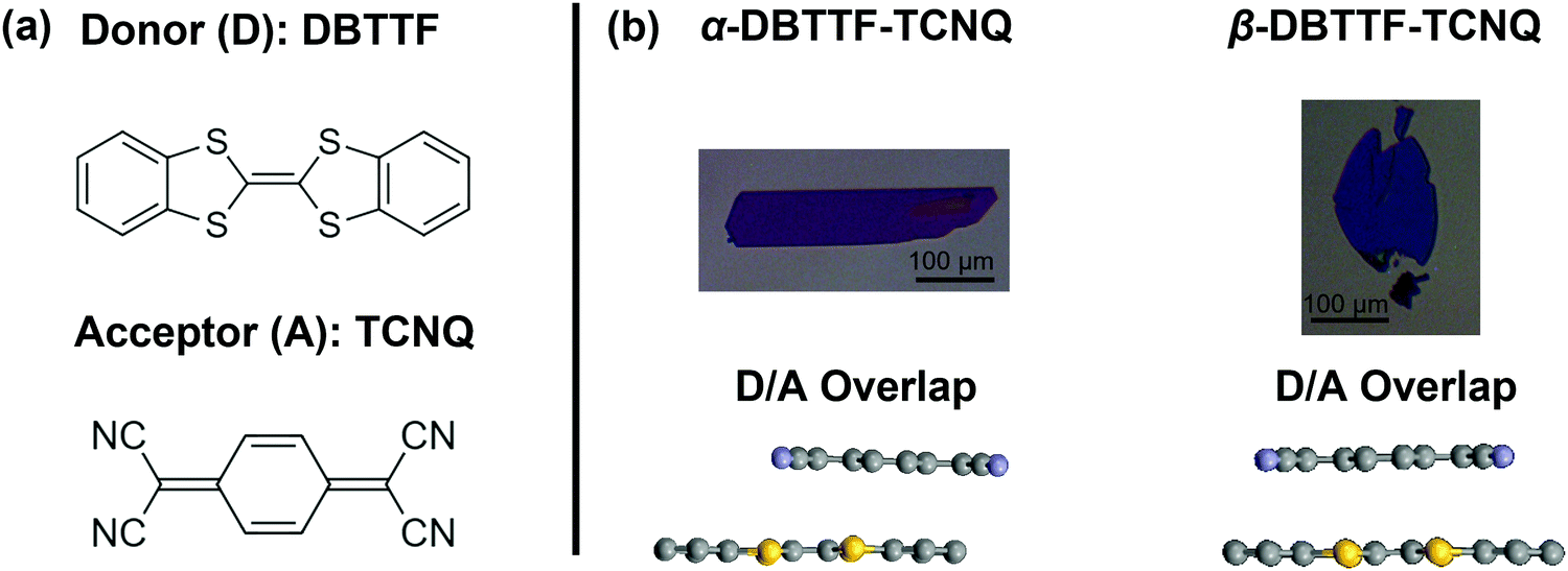 | ||
| Fig. 1 (a) The donor (DBTTF) and acceptor (TCNQ) in the CT complex. (b) Crystals of the α- and β-polymorphs, with the donor–acceptor overlap displayed below. The scale bars are 100 μm long. The α-polymorph is rectangular in habit, while the β-polymorph is elliptical and thin. The overlap is depicted from the crystal structure for the α-polymorph measured by X-ray diffraction, while the β-polymorph overlap is predicted based on selected-area electron diffraction measurements.23,43 The colors of the crystals are representative of their lamination onto a silicon wafer coated with 200 nm silicon dioxide. | ||
Results and discussions
Single crystals of DBTTF–TCNQ
Vapor-grown single crystals of polymorphic materials offer unique insight because they present an opportunity to minimize the sample-to-sample variation and access the intrinsic properties of each type of solid-state packing, in the absence of microstructure effects. To understand the impact of crystal structure on the electronic structure of DBTTF–TCNQ, we grew single crystals of the α- and β-polymorphs by the physical vapor transport method following a procedure described elsewhere.23 In short, the TCNQ was first purified by double sublimation prior to the solution crystallization of the CT complex. Because the vapor pressure of the parent compounds is comparable, we could then sublimate the solution-grown complex (as opposed to co-sublimating the parent compounds) to form the two polymorphs. The growth was completed over the course of several days, ensuring that impurity inclusion and point defect formation are as low as possible. The crystals, laminated on silicon dioxide (SiO2), are pictured in Fig. 1, where the α-polymorph forms into crystals with a rectangular habit, and the β-polymorph forms into elliptical crystals. In Fig. 1b, bottom panel, we included a side view of the D/A overlap, demonstrating a lateral shift in the co-facial crystal packing of one polymorph versus the other.23,43Field-effect transistor characterization
FETs were fabricated in the bottom-contact, top-gate geometry, as shown in Fig. 2a. The source/drain contacts were gold, the gate-dielectric was approximately 1000 μm parylene-N, and the gate electrode was silver. The transfer characteristics in the linear regime (source–drain voltage VDS = 2 V) for one crystal from each polymorph are shown in Fig. 2b, with transfer characteristics for VDS = −2 V and output characteristics being included in the ESI† (Section S1 and Fig. S1). The hole mobility for this device in the linear regime is approximately μh,lin = 0.01 cm2 V−1 s−1 for the α-polymorph, while the electron mobility in the linear regime is μe,lin = 0.1 cm2 V−1 s−1. Meanwhile, for the β-polymorph, μh,lin = 0.1 cm2 V−1 s−1, while μe,lin = 0.004 cm2 V−1 s−1. Transport was measured in the π-stack direction (the direction of the CT axis) for each polymorph. These values agree well with those previously reported in the saturation regime for the DBTTF–TCNQ polymorphs (μe,α = 0.4 ± 0.2 cm2 V−1 s−1, μh,α = 0.04 ± 0.02 cm2 V−1 s−1, μe,β = 0.03 ± 0.02 cm2 V−1 s−1, μh,β = 0.1 ± 0.07 cm2 V−1 s−1) with the present samples being approximately average, though we note that the electron mobility for the β-polymorph is on the lower end of what was previously reported.23 Such variations in the mobility values result from differences in crystal quality, anisotropy along different crystallographic directions, and contact resistance. For the α-DBTTF–TCNQ device the threshold voltage for electrons (VTh,e) was VTh,e = −2 V, while that for holes (VTh,h) was VTh,h = −12 V. Likewise, for β-DBTTF–TCNQ, VTh,h = −7 V, while VTh,e = 12 V.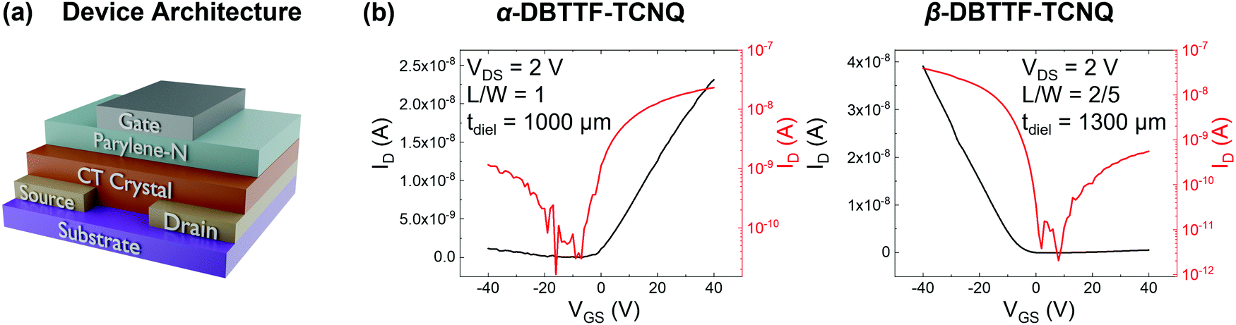 | ||
| Fig. 2 (a) The bottom-contact, top-gate transistor architecture used to extract the trap-DOS for each polymorph. (b) Examples of transfer characteristics in the linear regime for each polymorph. The VDS, channel dimensions as a ratio of length to width (L/W), and thickness of the parylene-N gate dielectric (tPary) are given in the inset. | ||
Electronic structure via angle-resolved photoemission spectroscopy
To access the electronic structure of each polymorph, we performed ARPES measurements on the α- and β-crystals, as well as their single-crystal parent components. The measurements of the HOMOs as a function of the azimuthal (θx) and polar (θy) angles of the photoelectron are shown for each crystal in Fig. 3a–d. Further information is reported in the ESI,† Section S2. All measurements are referenced to the Fermi energy, EF, rather than the ionization potential. The photoelectron emission angle is directly related to the in-plane momentum of the electron residing in the solid crystal; therefore, we are measuring the HOMO along different crystallographic directions. The HOMO can be discerned in the parent compound DBTTF (Fig. 3a), having a position center of 1.3 eV ± 0.1 eV below the Fermi energy and a full width at half maximum of 0.6 eV ± 0.1 eV. This is consistent with DBTTF UV photoemission spectra reported by others, and also in agreement with our measurements of thin-film DBTTF (ESI,† Section 2c and Table S1), except that we were not able to detect the HOMO−1 level in the DBTTF single crystal.44,45 The HOMO−1 should be about 1.5–2 eV below HOMO. Given the difficulty in measuring the HOMO in the DBTTF crystal (based on the signal-to-noise ratio compared to Fig. 3b–d for similar measurement statistics), it is not surprising that we could not resolve the deeper HOMO−1. We attribute this difficulty to the relatively small and thin DBTTF crystals that we measured when compared to the TCNQ, α-DBTTF–TCNQ, and β-DBTTF–TCNQ crystals. It may have been possible to resolve the HOMO−1 in the DBTTF crystal if we increased the measurement collection time or photon flux, but this may have degraded the crystal due to beam damage effects. For single-crystal TCNQ, two HOMOs were resolved, where HOMO and HOMO−1 are 3.5 eV ± 0.1 eV and 4.7 eV ± 0.1 eV below the Fermi energy, respectively (Fig. 3d). The HOMO and HOMO−1 widths are both estimated as 0.6 eV ± 0.1 eV. The electronic structure of TCNQ is consistent with our thin-film UV PES spectrum (ESI,† Section S2c and Table S1), and in good qualitative agreement with calculations where the leading HOMO does not show strong dispersion with momentum (i.e., emission angle) and the HOMO−1 is about 1 eV below the HOMO.46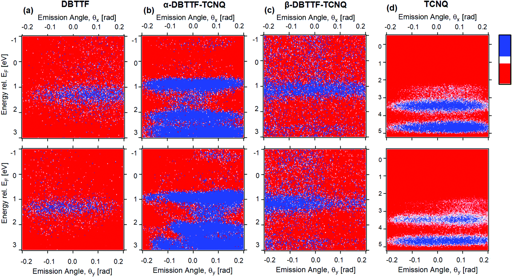 | ||
| Fig. 3 ARPES results of crystalline (a) DBTTF, (b) α-DBTTF–TCNQ, (c) β-DBTTF–TCNQ, and (d) TCNQ. Top and bottom panel show the electron emission as a function of θx and θy, respectively, and high counts shown in blue and low counts in red. The data are shown within the angular emission range of ±0.2 rad (corresponding to ±0.8 Å−1). | ||
The electronic structure of both α- and β-polymorphs of DBTTF–TCNQ are shown in Fig. 3b and c, with their respective HOMO centers lying at 0.9 eV ± 0.1 eV and 1.15 eV ± 0.1 eV below the Fermi energy. For the α-phase (Fig. 3b), multiple HOMOs are clearly visible, while for the β-phase, only the HOMO is discerned and possibly a HOMO−1, though it is faint. The α-phase HOMO−1 and HOMO−2 are centered at 2.15 eV ± 0.1 eV and 2.8 eV ± 0.1 eV, respectively. The α-phase HOMO and HOMO−1 width are 0.45 eV ± 0.1 eV and 0.3 eV ± 0.1 eV, while the width of HOMO−2 is difficult to estimate due to the strong background in that spectral regime. The α-phase HOMO width is consistent with the predicted result of about 0.5 eV.47 For the β-phase, the HOMO width is 0.6 eV ± 0.1 eV and weak signs of HOMO−1 are detected with a center of 2.7 eV ± 0.1 eV. We attribute the leading HOMO of both the α- and β-polymorphs to have DBTTF character based on the position of the HOMO in the DBTTF spectra (in Fig. 3a). For the α-polymorph, the HOMO−1 and HOMO−2 likely have attributes from both the DBTTF HOMO−1 and the TCNQ HOMO parent character (Fig. 3d). This is suggested by reported DBTTF gas-phase and thin-film measurements, and electronic property calculations of individual DBTTF and TCNQ.44–46,48 The energetic spacing and ordering (i.e., whether they originate from D or A) of the HOMOs within the CT complex crystal thus differ from the parent (D and A) electronic structure, and the leading orbitals of the CT complex are extremely sensitive to differences in packing geometry which in turn impacts the intermolecular interaction.21,49 Additionally, the molecular orientation with respect to the probed crystal facet (determined to be the molecular long axes for the α-polymorph and inferred to be the molecular short axes for the β-polymorph)23 would cause a variation in the ionization energies of each polymorph. We note that upon forming a CT complex, the leading HOMOs of the α- and β-polymorph have moved closer to the Fermi energy (when compared to the DBTTF parent) consistent with behavior expected in the CT complex as previously observed in the 4T-F4TCNQ co-crystal.20 Notably, the α-polymorph is closer to the Fermi energy than the β-polymorph, consistent with α-phase displaying a larger ionicity (degree of CT) than the β-phase.23 Intermolecular hybridization underpins CT complex systems in the ground state, where the CT complex HOMO is expected to lie between the HOMO of the D and A (when energy levels are referenced to the vacuum level).17,20 Our observed trend is consistent with intermolecular hybridization in molecular electrical doping.
In both the α- and β-polymorph crystals, there is a change in the leading HOMO width seen in the θy (Fig. 3b and c, bottom panel) which is in agreement with density functional theory (DFT) calculations; α-DBTTF–TCNQ was predicted to have a HOMO width of 0.5 eV with some dispersion.47 Little to no dispersion of the leading HOMO of both α- and β-phases is consistent with relatively small hole mobility values obtained via transport measurements. The observation of HOMOs and the presence of HOMO dispersion is likely highly dependent on the excitation photon energy; for single crystal pentacene, the HOMO dispersion was observed at photon energy of 10 eV, but not while measuring at higher photon energies, as is common for ARPES (here, we measured at 41 eV).50 Similar dependencies on the photon energy to the photoemission current have been extensively observed in few-layer graphene and has been theorized to be due to electron interference effects from adjacent layers.51,52
It is remarkable that for identical chemical composition and measurement conditions (excitation energy and intensity, measurement geometry and duration), we see qualitatively different electronic structure between the two polymorphs of DBTTF–TCNQ and probe multiple HOMOs for each polymorph (though weakly for the β-phase). Nevertheless, measuring the electronic structure was easier in the α-phase than the β-phase based on the overall signal to noise ratio. The differences detected in the HOMO of the two polymorphs by ARPES are a direct consequence of the variations in molecular packing in the crystalline solid, which impacts the photoemission selection rules (i.e., transition matrix element). In addition, the surfaces of the α- and β-polymorphs of DBTTF–TCNQ likely undergo different surface relaxation mechanisms from each other, which in turn could impact the ease of probing their electronic structure with ARPES. It has been shown that tetracene undergoes large surface relaxation and this is speculated to be the cause for the lack of observation of HOMO dispersion in ARPES.53 The structural differences of the polymorphs of DBTTF–TCNQ impacts its electronic structure and the ability to probe such HOMOs as gleaned from the photoemission results.
Density of trap states investigated by field-effect transistor measurements
The electronic structure has direct implications on the intrinsic charge transport within the crystal. Trap states present at the edge of the HOMO and extending into the bandgap, which form due to various intrinsic and extrinsic factors such as structural defects, chemical impurities, energetic disorder, or environmental contaminants, result in charge localization and inhibit charge transport.54–58 Therefore, in order to gain a complete picture of the electronic structure of both α- and β-polymorphs, we accessed the energetic distribution of the density of trap states (t-DOS) in the bandgap of the two types of crystals using the Grünewald method.57,59,60 This method for t-DOS extraction is typically performed on unipolar semiconductors, as it requires the identification of a potential at which the channel is flat. This condition does not always occur in ambipolar FETs, which may be always on, depending on the threshold voltages for holes and electrons relative to each other.61 Nevertheless, the large difference in threshold voltages for the electron and hole transport typical for our devices ensured that the FET channel was unipolar and flat for low drain–source voltages (VDS) and that we could identify an off state; therefore, we could reliably extract the t-DOS. The electron and hole trap distributions for the α-(black) and β-(red) polymorphs are plotted as a function of energy in the bandgap with respect to the approximate HOMO and LUMO edges in Fig. 4. The average mobility values for hole and electrons are included in the inset.23 To extract quantitative information on the density and energetics of traps, each t-DOS spectrum was modelled using a double exponential distribution to account for shallow (E1, N1) and deep traps (E2, N2), according to eqn (1):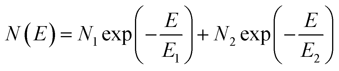 | (1) |
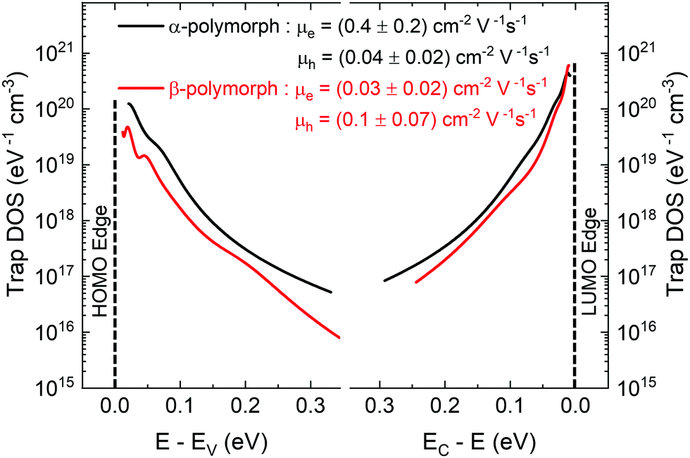 | ||
| Fig. 4 t-DOS spectra of electron and hole in α-(black) and β-(red) polymorphs shown with respect to the HOMO (Ev) and LUMO (Ec) edges. | ||
| Model parameter | α-polymorph | β-polymorph | ||
|---|---|---|---|---|
| Electrons | Holes | Electrons | Holes | |
| N 1 (eV−1 cm−3) | 7.4 × 10²⁰ | 3.1 × 10²⁰ | 9.2 × 10²⁰ | 8.7 × 10¹⁹ |
| E 1 (meV) | 18 | 24 | 12 | 22 |
| N 2 (eV−1 cm−3) | 1.2 × 10¹⁹ | 2.4 × 10¹⁸ | 3.0 × 10¹⁹ | 6.1 × 10¹⁸ |
| E 2 (meV) | 57 | 86 | 41 | 53 |
Discussions
The electronic structure determined by combining the results obtained from the ARPES and t-DOS measurements is summarized in Fig. 5. The values extracted for each HOMO and deeper levels are given for the CT polymorphs and the parent compounds in Fig. 5a. Fig. 5b shows the example of the β-polymorph HOMO level, which is not sharply defined – a typical feature of organic semiconductors – but is represented as a Gaussian curve, with the extended (mobile) states in the middle. Localized (trap) states are distributed exponentially below a HOMO or mobility edge.63 The nature of the charge carriers (whether they are localized or delocalized) is not probed in this study and so we choose to reference the constant mobility onset to the HOMO edge rather than the mobility edge.64 Mahraeen et al. showed that the constant mobility onset occurs where the exponential DOS, here defined by our trap measurement, and the Gaussian HOMO distribution meet.65 Also relevant to charge transport are the LUMO characteristics, which impact electron t-DOS for each polymorph.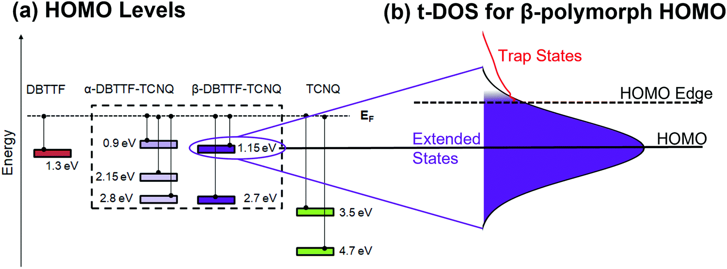 | ||
| Fig. 5 Electronic structure of α- and β-DBTTF–TCNQ. (a) A summary of the ARPES results shown in Fig. 3 of the identified HOMO levels of α-DBTTF–TCNQ, β-DBTTF–TCNQ, and each parent compound. Energy referencing is to the Fermi level. The uncertainty is ±0.1 eV to account for contact potential differences between Au and Ag substrates. (b) A schematic representation of the HOMO of β-DBTTF–TCNQ. The HOMO is represented by a Gaussian distribution, and the t-DOS calculation for holes is shown in red at the HOMO edge. | ||
With these results, we gain further insight into both the charge-transport polarities of each polymorph and the relationship between theoretical calculations and experiment. DFT calculations on the α-47 and β-polymorphs23 suggest that the hole and electron transport are balanced in both systems and more efficient in the α-polymorph; i.e., the transfer integrals are similar in magnitude for electrons and holes in each case, and higher in the α-polymorph by almost an order of magnitude. Experimental results extracted from FET work, however, have not been able to confirm these predictions. Comparisons between theory and experiment are inherently challenging when there are unavoidable extrinsic parameters in the measurement. It is tempting to hypothesize about the nature of the contacts, and subsequently, compare hole mobility for each polymorph, based on an approximate energetic barrier between the work function of the gold source/drain electrodes and the HOMO levels; however, the complex processes occurring when the electrode and semiconductor materials are brought into contact can modify the band diagram, and hence the contact resistance significantly.66 Indeed, the ARPES results suggest that the energetic barriers for holes for each polymorph are very similar, and therefore, do not account for the extent of the variation in charge transport polarities between the polymorphs.
A possible explanation for this behavior is the formation of a more favorable pathway for electron versus hole transport, or vice-versa, due to the differences in the crystal structures between α- and β-DBTTF–TCNQ. Recent research on the DFT methodology for mixed-stack CT systems and D–A co-polymers has explored the role of the molecular orbitals of the bridge molecules in charge transport under the super-exchange theory.21,67–72 Here, because of the D–A–D–A… nature of the mixed-stack crystal structure, the distance between one donor molecule and the next (or one acceptor molecule and the next) is high and the direct D–D or A–A coupling is low. Transport then proceeds via the bridging A (for the D–A–D trimer) or D (for the A–D–A trimer) molecule. If bridge orbitals underlying the frontier HOMO and LUMO levels (i.e. HOMO−1, LUMO−1, etc.) contribute to transport, then the balance between charge carriers can favor holes more than electrons or vice-versa. Transport measurements in other systems are also suggestive of such a transport mechanism.73,74 The varying relative positions of the HOMO, HOMO−1, and deeper levels measured in the DBTTF–TCNQ polymorphs via ARPES could be an indication that this is the case here; however, definitive insight would require further theoretical investigation.
Trap states, as shown in Fig. 4, induce a further reduction in charge-carrier mobility from the intrinsic value. The electron mobilities in both polymorphs are significantly reduced in a real crystal due to the fact that electrons are more easily trapped than holes in the presence of oxygen and water under typical operating conditions, in agreement with the overall trap density for electrons being higher than holes in both polymorphs in Fig. 4.75 Interestingly, in spite of the fact that in the α-polymorph the density of electron traps is higher than the density of hole traps (more than twice as many shallow electron traps, N1, and an order of magnitude higher deep electron traps, N2), a more efficient electron transport is characteristic for this solid state packing,41 with some reports finding no signature of a p-type channel.39 One reason for this behavior is that when the density of shallow traps (N1) is sufficiently high, then charge carriers can hop between one localized shallow trap state to another, thereby, contributing to charge transport.54 Additionally, the characteristic width of the trap distribution for holes is broader than for electrons for the same polymorph (∼30% and ∼50% broader shallow trap distribution, E1, and deep hole trap distribution, E2, respectively), indicating that the hole traps extend further into the bandgap, increasing the likelihood of hole trapping events, which in turn can inhibit efficient hole transport.54 Other factors in charge-transport yet to be examined, such as dynamic disorder, may play an additional role in reducing hole transport further than electron transport.76 The exceptionally low hole trap density found in the α-polymorph could explain our observation of hole transport, confirming the importance of the crystal quality in accessing intrinsic properties, which are not dominated by the trap environment. Similar to the case of the α-polymorph, in the β-polymorph, the electron trap density is higher than the hole trap density, but in this case, the difference is more pronounced with an order of magnitude gap for both shallow and deep traps. This aligns with the electron transport being less efficient in our device studies and suggest that for this packing the additional charge transport pathways are inhibited. Theoretical studies examining the relationship between transport and the participation of differing energy levels in transport may shed further light on this phenomenon.
Conclusions
In conclusion, we studied a highly ordered donor–acceptor system based on single crystals, which provided a reliable experimental platform for the examination of the electronic structure and sub-gap density of trap states in relation to the solid-state packing. ARPES measurements reveal an energetic shift in the HOMO and HOMO−1 positions relative to EF, depending on the co-facial overlap of the donor and acceptor units. A HOMO−2 state is also apparent in the α-polymorph. The t-DOS was accessed through FET measurements in the linear (flat-band) regime, showing a higher overall density of electron traps in each polymorph versus hole traps, with the α-polymorph being more susceptible to trap formation than the β-polymorph. The impact of these results is two-fold. First, they shed light on the critical contribution of varying energy level contributions and trap states on the charge transport properties of organic crystals. Second, they present a method by which to understand donor–acceptor interactions in the absence of microstructural and other changes to extrinsic factors. We expect these results to be useful in understanding how varying co-facial overlap can alter the CT state energetics and charge-carrier trapping in applications such as doping, where a clear picture of charge transport is currently lacking.Methods
Crystal growth
Crystals of the two polymorphs of DBTTF–TCNQ were grown by the physical vapor transport (PVT) method following the procedure described in detail elsewhere. In brief, the CT complex DBTTF–TCNQ was prepared via solution diffusion of the parent compounds in acetonitrile, which was saturated at approximately 60 °C and then slow cooled. The collected crystals were dried and placed in the vapor furnace. This source material was heated to 170 °C under an argon flow of 150 mL min−1. The α-polymorph formed in flat, rectangle-shaped crystals in a region between room temperature and 45 °C, while the β-polymorph formed in flat, ellipse-shaped crystals between 40 °C and 65 °C. All crystal growth took place on quartz tubing. DBTTF and TCNQ crystals were grown in a similar fashion at 225 °C and 175 °C respectively.Angle-resolved photoemission spectroscopy
ARPES electronic structure measurements were carried out at the BESSY II synchrotron facility (Helmholtz-Zentrum Berlin) on beamline PM4.1 This beamline is equipped with a high-detection efficiency, angle-resolved time-of-flight (ARTOF) spectrometer that allows simultaneous collection of angle-resolved photoemission data over a large solid angle (±15° or ±0.26 rad) while maintaining a low total soft X-ray dose on the organic single crystal.77 Measurements were performed at room temperature with a photon energy of 41 eV for DBTTF and DBTTF–TCNQ compounds, and 85 eV for TCNQ, and the energy scale was referenced to the Fermi energy of a Au and Ag sample at those photon energies. The uncertainty is ±0.1 eV to account for contact potential differences between Au and Ag substrates as determined by the difference of the work function of these air-exposed substrates (see Section 2c of the ESI†). Ionization energy referencing was not possible due to the inability to perform reliable work function measurements by photoemission due to the small size of the crystals. Photoemission measurements were performed on one crystal laminated onto Au or Ag substrates with painted Ag contacts along the edges. All spectra were corrected to remove the underlying contribution from either the Au or Ag substrate in which the crystals were mounted. HOMO width is estimated from the integrated spectra as the full-width at half maximum. ARPES measurements were aided by a cw laser (473 nm) to increase the conductivity in the sample. The geometries of the excitation source and electron energy analyzer used for measurement as well as the bipolar coordinate system used for the presentation of the ARTOF data are also shown in ref. 67.78 Here, the ARPES data are shown with an angular emission in the range of ±0.2 rad (corresponding to ±0.8 Å−1).Transistor fabrication and characterization
Transistors were prepared in the top-gate, bottom-contact geometry.79 Substrates of heavily n++ doped Si with 200 nm of thermally oxidized SiO2 were cleaned in hot acetone and isopropanol, 10 minutes UV-Ozone, rinsed with DI-water, and dried with nitrogen, sequentially. 5 nm Ti/45 nm Au source/drain electrodes were patterned using a shadow mask and deposited via e-beam evaporation. Crystals were laminated by hand onto the substrate and were thin enough to stick via electrostatic adhesion. For the gate dielectric, 750–1000 nm N-parylene (εr = 2.65, thickness determined via capacitance and profilometry) was deposited via a procedure described elsewhere.80 Silver (60 nm) was thermally evaporated for the gate electrode (0.5–1 Å s−1). Electrical properties were measured in air and in the dark using an Agilent 4155C semiconductor parameter analyzer.81Trap DOS analysis
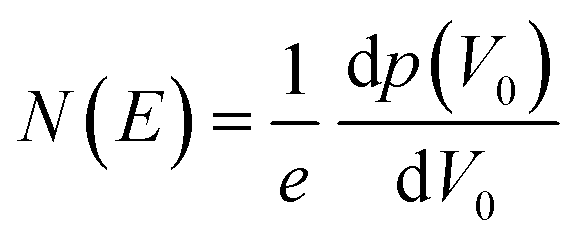
The trap density of states was determined from the linear-regime transfer characteristics of the FETs following Grünewald method.54,57,60,82 The hole and electron trap distributions were evaluated using the region of the transfer curves where hole-only and electron-only transport was observed.The gate-voltage dependent interface potential function V0 (UGS) resulting from the energy level bending at the OSC/dielectric interface was derived based on the gate-source voltage UGS above the flat-band voltage VFB, i.e., UGS = |VGS − VFB|, where VFB is assumed to be the turn-on voltage (VON) of the device the gate-voltage.57,83 The value for VON was determined as the point where the current rose above the noise of the off state of the transistor. The trap DOS was obtained by numerically differentiating the total hole density with respect to V0. I.e.,
 | (2) |
Conflicts of interest
There are no conflicts to declare.Acknowledgements
The work at Wake Forest University was supported by the National Science foundation through Grants No. DMR-1627925 and ECCS-1810273. We thank Dr Steven Robey for assistance with the ARPES measurements, Drs Erika Giangrisostomi and Ruslan Ovsyannikov for their support during the beamtime, and the Helmholtz Zentrum Berlin for the allocation of synchrotron radiation beamtime.References
- S. Fratini, M. Nikolka, A. Salleo, G. Schweicher and H. Sirringhaus, Nat. Mater., 2020, 19, 491–502 CrossRef CAS.
- A. M. Zeidell, D. S. Filston, M. Waldrip, H. F. Iqbal, H. Chen, I. McCulloch and O. D. Jurchescu, Adv. Mater. Technol., 2020, 5, 2000390 CrossRef CAS.
- A. Karki, A. J. Gillett, R. H. Friend and T. Nguyen, Adv. Energy Mater., 2021, 11, 2003441 CrossRef CAS.
- Y. Lin, B. Adilbekova, Y. Firdaus, E. Yengel, H. Faber, M. Sajjad, X. Zheng, E. Yarali, A. Seitkhan, O. M. Bakr, A. El-Labban, U. Schwingenschlögl, V. Tung, I. McCulloch, F. Laquai and T. D. Anthopoulos, Adv. Mater., 2019, 31, 1902965 CrossRef CAS.
- J. Rivnay, S. Inal, A. Salleo, R. M. Owens, M. Berggren and G. G. Malliaras, Nat. Rev. Mater., 2018, 3, 17086 CrossRef CAS.
- A. Melianas, T. J. Quill, G. LeCroy, Y. Tuchman, H. V. Loo, S. T. Keene, A. Giovannitti, H. R. Lee, I. P. Maria, I. McCulloch and A. Salleo, Sci. Adv., 2020, 6, eabb2958 CrossRef CAS.
- J. Martín, D. Zhao, T. Lenz, I. Katsouras, D. M. De Leeuw and N. Stingelin, Mater. Horiz., 2017, 4, 408–414 RSC.
- K. A. Peterson, E. M. Thomas and M. L. Chabinyc, Annu. Rev. Mater. Res., 2020, 50, 551–574 CrossRef CAS.
- J. W. Borchert, U. Zschieschang, F. Letzkus, M. Giorgio, R. T. Weitz, M. Caironi, J. N. Burghartz, S. Ludwigs and H. Klauk, Sci. Adv., 2020, 6, eaaz5156 CrossRef CAS PubMed.
- J. Liu, B. van der Zee, R. Alessandri, S. Sami, J. Dong, M. I. Nugraha, A. J. Barker, S. Rousseva, L. Qiu, X. Qiu, N. Klasen, R. C. Chiechi, D. Baran, M. Caironi, T. D. Anthopoulos, G. Portale, R. W. A. Havenith, S. J. Marrink, J. C. Hummelen and L. J. A. Koster, Nat. Commun., 2020, 11, 1–9 Search PubMed.
- X.-K. Chen, D. Qian, Y. Wang, T. Kirchartz, W. Tress, H. Yao, J. Yuan, M. Hülsbeck, M. Zhang, Y. Zou, Y. Sun, Y. Li, J. Hou, O. Inganäs, V. Coropceanu, J.-L. Bredas and F. Gao, Nat. Energy, 2021, 6, 799–806 CrossRef CAS.
- A. Salehi, C. Dong, D.-H. Shin, L. Zhu, C. Papa, A. Thy Bui, F. N. Castellano and F. So, Nat. Commun., 2019, 10, 2305 CrossRef PubMed.
- R. Kroon, D. A. Mengistie, D. Kiefer, J. Hynynen, J. D. Ryan, L. Yu and C. Müller, Chem. Soc. Rev., 2016, 45, 6147–6164 RSC.
- B. Lüssem, C.-M. Keum, D. Kasemann, B. Naab, Z. Bao and K. Leo, Chem. Rev., 2016, 116, 13714–13751 CrossRef.
- I. Salzmann, G. Heimel, M. Oehzelt, S. Winkler and N. Koch, Acc. Chem. Res., 2016, 49, 370–378 CrossRef CAS.
- D. Kiefer, R. Kroon, A. I. Hofmann, H. Sun, X. Liu, A. Giovannitti, D. Stegerer, A. Cano, J. Hynynen, L. Yu, Y. Zhang, D. Nai, T. F. Harrelson, M. Sommer, A. J. Moulé, M. Kemerink, S. R. Marder, I. McCulloch, M. Fahlman, S. Fabiano and C. Müller, Nat. Mater., 2019, 18, 149–155 CrossRef CAS.
- I. Salzmann, G. Heimel, S. Duhm, M. Oehzelt, P. Pingel, B. M. George, A. Schnegg, K. Lips, R.-P. Blum, A. Vollmer and N. Koch, Phys. Rev. Lett., 2012, 108, 035502 CrossRef.
- C. Deibel, T. Strobel and V. Dyakonov, Adv. Mater., 2010, 22, 4097–4111 CrossRef CAS.
- I. E. Jacobs and A. J. Moulé, Adv. Mater., 2017, 29, 1703063 CrossRef.
- H. Méndez, G. Heimel, S. Winkler, J. Frisch, A. Opitz, K. Sauer, B. Wegner, M. Oehzelt, C. Röthel, S. Duhm, D. Többens, N. Koch and I. Salzmann, Nat. Commun., 2015, 6, 8560 CrossRef.
- H. Geng, X. Zheng, Z. Shuai, L. Zhu and Y. Yi, Adv. Mater., 2015, 27, 1443–1449 CrossRef CAS.
- I. E. Jacobs, C. Cendra, T. F. Harrelson, Z. I. Bedolla Valdez, R. Faller, A. Salleo and A. J. Moulé, Mater. Horiz., 2018, 5, 655–660 RSC.
- K. P. Goetz, J. J. Tsutsumi, S. Pookpanratana, J. Chen, N. S. Corbin, R. K. Behera, V. Coropceanu, C. A. Richter, C. A. Hacker, T. Hasegawa and O. D. Jurchescu, Adv. Electron. Mater., 2016, 2, 1600203 CrossRef PubMed.
- T. Mori and H. Inokuchi, Solid State Commun., 1986, 59, 355–359 CrossRef CAS.
- H. M. Yamamoto, M. Hagiwara and R. Kato, Synth. Met., 2003, 133–134, 449–451 CrossRef CAS.
- P. Guionneau, C. J. Kepert, G. Bravic, D. Chasseau, M. R. Truter, M. Kurmoo and P. Day, Synth. Met., 1997, 86, 1973–1974 CrossRef CAS.
- S. Flandrois and D. Chasseau, Acta Crystallogr., Sect. B: Struct. Crystallogr. Cryst. Chem., 1977, 33, 2744–2750 CrossRef.
- T. C. Umland, S. Allie, T. Kuhlmann and P. Coppens, J. Phys. Chem., 1988, 92, 6456–6460 CrossRef CAS.
- D. A. Stanfield, Y. Wu, S. H. Tolbert and B. J. Schwartz, Chem. Mater., 2021, 33, 2343–2356 CrossRef CAS.
- K. E. Watts, B. Neelamraju, E. L. Ratcliff and J. E. Pemberton, Chem. Mater., 2019, 31, 6986–6994 CrossRef CAS.
- K. P. Goetz, D. Vermeulen, M. E. Payne, C. Kloc, L. E. McNeil and O. D. Jurchescu, J. Mater. Chem. C, 2014, 2, 3065–3076 RSC.
- J. Zhang, J. Jin, H. Xu, Q. Zhang and W. Huang, J. Mater. Chem. C, 2018, 6, 3485–3498 RSC.
- J. Zhang, W. Xu, P. Sheng, G. Zhao and D. Zhu, Acc. Chem. Res., 2017, 50, 1654–1662 CrossRef CAS PubMed.
- S. Horiuchi, T. Hasegawa and Y. Tokura, J. Phys. Soc. Jpn., 2006, 75, 051016 CrossRef.
- R. R. Dasari, X. Wang, R. A. Wiscons, H. F. Haneef, A. Ashokan, Y. Zhang, M. S. Fonari, S. Barlow, V. Coropceanu, T. V. Timofeeva, O. D. Jurchescu, J. Brédas, A. J. Matzger and S. R. Marder, Adv. Funct. Mater., 2019, 29, 1904858 CrossRef CAS.
- J. Ferraris, D. O. Cowan, V. Walatka and J. H. Perlstein, J. Am. Chem. Soc., 1973, 95, 948–949 CrossRef CAS.
- J. Zhang, H. Geng, T. S. Virk, Y. Zhao, J. Tan, C. Di, W. Xu, K. Singh, W. Hu, Z. Shuai, Y. Liu and D. Zhu, Adv. Mater., 2012, 24, 2603–2607 CrossRef CAS.
- D. Jerome, A. Mazaud, M. Ribault and K. Bechgaard, J. Phys., Lett., 1980, 41, 95–98 CrossRef CAS.
- Y. Takahashi, T. Hasegawa, Y. Abe, Y. Tokura, K. Nishimura, G. Saito, J. Hasegawa, Y. Abe, Y. Tokura, K. Nishimura and G. Saito, Appl. Phys. Lett., 2005, 86, 063504 CrossRef.
- Y. Takahashi, T. Hasegawa, Y. Abe, Y. Tokura and G. Saito, Appl. Phys. Lett., 2006, 88, 073504 CrossRef.
- H.-D. Wu, F.-X. Wang, Y. Xiao and G.-B. Pan, J. Mater. Chem. C, 2013, 1, 2286–2289 RSC.
- A. Girlando, Adv. Electron. Mater., 2017, 3, 1600437 CrossRef.
- T. J. Emge, F. M. Wiygul, J. S. Chappell, A. N. Bloch, J. P. Ferraris, D. O. Cowan and T. J. Kistenmacher, Mol. Cryst. Liq. Cryst., 1982, 87, 137–161 CrossRef CAS.
- N. Sato, H. Inokuchi and I. Shirotani, Chem. Phys., 1981, 60, 327–333 CrossRef CAS.
- J. Spanget-Larsen, R. Gleiter and S. Hünig, Chem. Phys. Lett., 1976, 37, 29–32 CrossRef CAS.
- Y. Krupskaya, M. Gibertini, N. Marzari and A. F. Morpurgo, Adv. Mater., 2015, 27, 2453–2458 CrossRef CAS PubMed.
- L. Zhu, Y. Yi, Y. Li, E. G. Kim, V. Coropceanu and J. L. Brédas, J. Am. Chem. Soc., 2012, 134, 2340–2347 CrossRef CAS.
- J. Casado, M. Z. Zgierski, M. C. R. Delgado, J. T. L. Navarrete, M. Mas-Torrent and C. Rovira, J. Phys. Chem. C, 2007, 111, 10110–10118 CrossRef CAS.
- C. Park, V. Atalla, S. Smith and M. Yoon, ACS Appl. Mater. Interfaces, 2017, 9, 27266–27272 CrossRef CAS.
- Y. Nakayama, S. Kera and N. Ueno, J. Mater. Chem. C, 2020, 8, 9090–9132 RSC.
- E. Krasovskii, Nanomaterials, 2021, 11, 1212 CrossRef CAS.
- P. Ayria, A. R. T. Nugraha, E. H. Hasdeo, T. R. Czank, S. Tanaka and R. Saito, Phys. Rev. B: Condens. Matter Mater. Phys., 2015, 92, 195148 CrossRef.
- H. Morisaki, T. Koretsune, C. Hotta, J. Takeya, T. Kimura and Y. Wakabayashi, Nat. Commun., 2014, 5, 5400 CrossRef CAS PubMed.
- H. F. Haneef, A. M. Zeidell and O. D. Jurchescu, J. Mater. Chem. C, 2020, 8, 759–787 RSC.
- P. J. Diemer, J. Hayes, E. Welchman, R. Hallani, S. J. Pookpanratana, C. A. Hacker, C. A. Richter, J. E. Anthony, T. Thonhauser and O. D. Jurchescu, Adv. Electron. Mater., 2017, 3, 1600294 CrossRef.
- W. Kalb, K. Mattenberger and B. Batlogg, Phys. Rev. B: Condens. Matter Mater. Phys., 2008, 78, 035334 CrossRef.
- H. F. Iqbal, Q. Ai, K. J. Thorley, H. Chen, I. McCulloch, C. Risko, J. E. Anthony and O. D. Jurchescu, Nat. Commun., 2021, 12, 2352 CrossRef CAS.
- D. Venkateshvaran, M. Nikolka, A. Sadhanala, V. Lemaur, M. Zelazny, M. Kepa, M. Hurhangee, A. J. Kronemeijer, V. Pecunia, I. Nasrallah, I. Romanov, K. Broch, I. McCulloch, D. Emin, Y. Olivier, J. Cornil, D. Beljonne and H. Sirringhaus, Nature, 2014, 515, 384–388 CrossRef CAS.
- M. Grünewald, P. Thomas and D. Würtz, Phys. Status Solidi, 1980, 100, K139–K143 CrossRef.
- W. L. Kalb and B. Batlogg, Phys. Rev. B: Condens. Matter Mater. Phys., 2010, 81, 035327 CrossRef.
- M. S. Kang and C. D. Frisbie, ChemPhysChem, 2013, 14, 1547–1552 CrossRef CAS PubMed.
- V. Coropceanu, J. Cornil, D. A. da Silva Filho, Y. Olivier, R. Silbey and J.-L. Brédas, Chem. Rev., 2007, 107, 926–952 CrossRef CAS.
- S. N. Mott, J. Phys. C: Solid State Phys., 1987, 20, 3075–3102 CrossRef.
- G. Horowitz, J. Appl. Phys., 2015, 118, 115502 CrossRef.
- S. Mehraeen, V. Coropceanu and J. L. Brédas, Phys. Rev. B: Condens. Matter Mater. Phys., 2013, 87, 1–9 CrossRef.
- M. Waldrip, O. D. Jurchescu, D. J. Gundlach and E. G. Bittle, Adv. Funct. Mater., 2020, 30, 1904576 CrossRef CAS.
- H. Geng, L. Zhu, Y. Yi, D. Zhu and Z. Shuai, Chem. Mater., 2019, 31, 6424–6434 CrossRef CAS.
- Y. Kato, H. Matsumoto and T. Mori, J. Phys. Chem. A, 2021, 125, 146–153 CrossRef CAS PubMed.
- K. Iijima, R. Sanada, D. Yoo, R. Sato, T. Kawamoto and T. Mori, ACS Appl. Mater. Interfaces, 2018, 10, 10262–10269 CrossRef CAS.
- R. Sato, T. Kawamoto and T. Mori, J. Mater. Chem. C, 2019, 7, 567–577 RSC.
- C. Cheng, H. Geng, Y. Yi and Z. Shuai, J. Mater. Chem. C, 2017, 5, 3247–3253 RSC.
- F. He, C. Cheng, H. Geng, Y. Yi and Z. Shuai, J. Mater. Chem. A, 2018, 6, 11985–11993 RSC.
- D. Vermeulen, L. Y. Zhu, K. P. Goetz, P. Hu, H. Jiang, C. S. Day, O. D. Jurchescu, V. Coropceanu, C. Kloc and L. E. McNeil, J. Phys. Chem. C, 2014, 118, 24688–24696 CrossRef CAS.
- S. Yokokura, Y. Takahashi, H. Nonaka, H. Hasegawa, J. Harada, T. Inabe, R. Kumai, H. Okamoto, M. M. Matsushita and K. Awaga, Chem. Mater., 2015, 27, 4441–4449 CrossRef CAS.
- L. Chua, J. Zaumseil, J. Chang, E. C.-W. Ou, P. K.-H. Ho, H. Sirringhaus and R. H. Friend, Nature, 2005, 434, 194–199 CrossRef CAS.
- S. Fratini, S. Ciuchi, D. Mayou, G. T. De Laissardière and A. Troisi, Nat. Mater., 2017, 16, 998–1002 CrossRef CAS.
- E. Giangrisostomi, R. Ovsyannikov, F. Sorgenfrei, T. Zhang, A. Lindblad, Y. Sassa, U. B. Cappel, T. Leitner, R. Mitzner, S. Svensson, N. Mårtensson and A. Föhlisch, J. Electron Spectrosc. Relat. Phenom., 2018, 224, 68–78 CrossRef CAS.
- S. J. Pookpanratana, K. P. Goetz, E. G. Bittle, H. Haneef, L. You, C. A. Hacker, S. W. Robey, O. D. Jurchescu, R. Ovsyannikov and E. Giangrisostomi, Org. Electron., 2018, 61, 157–163 CrossRef CAS.
- Z. A. Lamport, H. F. Haneef, S. Anand, M. Waldrip and O. D. Jurchescu, J. Appl. Phys., 2018, 124, 071101 CrossRef.
- V. Podzorov, V. M. Pudalov and M. E. Gershenson, Appl. Phys. Lett., 2003, 82, 1739–1741 CrossRef CAS.
- The identification of commercial equipment or vendor is not intended to imply recommendation or endorsement by NIST, nor is it intended to imply that the materials or equipment identified are necessarily the best available for the purpose.
- M. Geiger, L. Schwarz, U. Zschieschang, D. Manske, J. Pflaum, J. Weis, H. Klauk and R. T. Weitz, Phys. Rev. Appl., 2018, 10, 044023 CrossRef CAS.
- H. F. Iqbal, E. K. Holland, J. E. Anthony and O. D. Jurchescu, Mater. Horiz., 2020, 7, 2390–2398 RSC.
Footnote |
| † Electronic supplementary information (ESI) available. See DOI: 10.1039/d1mh01214b |
| This journal is © The Royal Society of Chemistry 2022 |