
 Open Access Article
 This Open Access Article is licensed under a
 Creative Commons Attribution 3.0 Unported Licence
Electronic properties of metal halide perovskites and their interfaces: the basics
Fengshuo
Zu
a,
Dongguen
Shin
 a and
Norbert
Koch
*ab
a and
Norbert
Koch
*ab
aInstitut für Physik & IRIS Adlershof, Humboldt-Universität zu Berlin, 12489 Berlin, Germany. E-mail: norbert.koch@physik.hu-berlin.de
bHelmholtz-Zentrum Berlin für Materialien und Energie GmbH, 12489 Berlin, Germany
First published on 28th August 2021
Abstract
We have witnessed tremendous progress of metal halide perovskite (MHP)-based optoelectronic devices, especially in the field of photovoltaics. Despite intensive research in the past few years, questions still remain regarding their fundamental optoelectronic properties, among which the electronic properties exhibit an interplay of numerous phenomena that deserve serious scrutiny. In this Focus article, we aim to provide a contemporary understanding of the unique electronic properties that has been resolved by the community. First introducing some of the basic concepts established in semiconductor physics, the intrinsic and extrinsic electronic properties of the MHPs are disentangled and explained. With this, the complex interplay of interface-, dopant-, and surface state-induced electronic states in determining the electrostatic landscape in the material can be comprehended, and the energy level alignment in device architectures more reliably assessed.
 Fengshuo Zu | Fengshuo Zu received his doctorate in physics from the Department of Physics, Humboldt-Universität zu Berlin (HU Berlin) in 2019. At present he is a postdoctoral researcher in the group of Norbert Koch at HU Berlin. His research mainly focuses on the fundamental electronic properties of metal halide perovskites and the energy level alignment at perovskite-related surfaces and interfaces using photoemission spectroscopy. |
 Dongguen Shin | Dongguen Shin received his doctorate in physics in 2019 from Yonsei University, Republic of Korea. He is currently working as a postdoctoral fellow in the group of Norbert Koch at the Department of Physics, Humboldt-Universität zu Berlin. His research interests concern the electronic properties of metal halide perovskites and two-dimensional transition metal dichalcogenides. |
 Norbert Koch | Norbert Koch received a doctorate in solid state physics from Technische Universität Graz in 2000. After two years as postdoc at Princeton University, he was independent junior research group leader at the Department of Physics, Humboldt-Universität zu Berlin, where he was appointed as full professor in 2009. In 2010 his group at the Helmholtz-Zentrum Berlin für Materialien und Energie was established. His research agenda focuses on interfacial phenomena of organic semiconductors, perovskites, and 2D semiconductors. |
1. Introduction
The unique structural and optoelectronic properties of metal halide perovskites (MHPs) have led to tremendous success in a variety of optoelectronic devices,1–5 and in particular in the field of photovoltaics.1,5 Despite an impressive body of research, it is still very challenging to draw a comprehensive picture of some of the fundamental properties of these semiconductors. This also pertains to the electronic properties of MHPs, which are key for achieving the full potential of these materials in applications. In many reports on MHP-based devices we can see schematic diagrams of how the frontier energy levels of the involved materials align relative to each other, but these diagrams are predominately presumed from pertinent parameters that were reported for the individual materials. Typically, the ionization energy (IE), electron affinity (EA), and work function (Φ) values are plotted next to each other with a constant electrostatic potential (often termed vacuum level and set to zero) across all interfaces. In lieu of an actual measurement of the energy level alignment, an assumed level diagram can be a useful zeroth-order approximation, but one should be aware of the fact that it may be far off from the actual situation encountered in a device. One underlying reason is that the IE, Φ, and EA are defined via the removal/attachment of an electron from/to the sample surface. Therefore, their values are not constant for a given material but they are significantly influenced by the atomic composition and structure, not only of the bulk, but particularly of the surface. In addition to preparation-dependent MHP surface variations, sample environment-dependent adsorbates can further influence the three key energy level parameters. Next, atomic-scale structural defects, such as vacancies and interstitials, can be electronically active and result in p- or n-type doping of the MHP bulk. At the surface of a sample defects can pin the Fermi level (EF) and induce surface band bending. Finally, extrinsic dopants can additionally vary the doping level of the semiconductor – near the surface or in the bulk.While each individual aspect named above is well known from other well-established semiconductors and can be investigated and understood also for MHPs, huge challenge arises for these materials from the simultaneous occurrence of more than one of these effects. This makes it often difficult to disentangle the impact of each in experiment, as observed from apparent inconsistencies reported during the early stage of research on MHPs.6–14 Studies on the intrinsic and extrinsic electronic properties of the MHPs continue to be demanding because of their tendency towards degradation or defect formation upon perturbation,15,16i.e., depending on experimental conditions these perovskites should be considered “living materials”. Overall, an estimated energy level diagram may be off with respect to the actual level alignment by several 100 meV, which can introduce serious problems when trying to link energy levels and devices performance.
The goal of this Focus article is to introduce the concepts of semiconductor electronic properties and energy levels for the most widely studied MHPs, with restriction to those bulk, surface, and interface effects that appear to be on a solid foundation at present. With the diverse composition of the MHP-community in mind, this should help researchers that are not concerned with the electronic structure on an every-day basis to make better informed and critical judgements on how to use published data on MHP electronic properties for their own purpose.
2. Intrinsic electronic band structure and determination of band edges
The ABX3 structure of MHPs typically comprises a corner-sharing BX6 octahedral cage, where B is a bivalent metal cation (e.g. Pb2+ or Sn2+), X a halide anion (e.g. I−, Br−, or Cl−), and a cation [often methylammomium (MA), formamidinium (FA), or Cs+] in the interstices. Studies on the crystal structure revealed that many MHPs exhibit phase transitions upon changing the temperature (T). For instance, the prototypical methylammonium lead triiodide (MAPbI3) was shown to undergo a structural transition from tetragonal at room temperature to cubic at higher temperature (T >327 K),17,18 owing to the fact that the MA cation exhibits different degrees of disorder at elevated temperature, accompanied by a slight distortion of the PbI6 octahedral cage.19 In contrast to bulk-sensitive methods, transmission electron microscopy20 and low-energy electron diffraction11 suggested that for MAPbI3 in ultra-thin slabs and at the surface of thin films in vacuum tetragonal and cubic phases coexist already at room temperature. It has not yet been shown whether higher ambient pressure or deposition of another material onto a mixed-phase surface stabilizes the tetragonal phase at room temperature again, and this may be a device-relevant aspect for future studies.The electronic band structure of the MHPs was investigated by several theoretical studies within the framework of density functional theory (DFT).21–24 While DFT is a powerful tool to predict the electronic and optical properties of functional materials, it can fail to provide accurate band gaps.25 Depending on the levels of theory being applied and the extent to which dispersive interactions and many-body effects are taken into account, e.g., spin–orbit coupling,26 the computed electronic band structure can vary considerably. Therefore, careful evaluation of the chosen method's reliability is indispensable.27,28 The calculations on MHPs were performed mostly on single cation and halide perovskites, e.g., MAPbX323 and CsPbX3,24 due to their simpler unit cell compared to the mixed-cation and mixed-halide counterparts. The electronic band structure is affected by structural changes, often leading to a shift of the fundamental band gap from the Brillouin zone (BZ) center in the tetragonal phase to a BZ edge in cubic phase, as schematically given in Fig. 1. Experimentally, the electronic structure of the MHPs has been and continues to be studied by means of photoelectron spectroscopy (PES). PES is based on measuring the kinetic energy and angular distributions of photoelectrons emitted from a sample surface upon excitation with monochromatic light. It is widely used for assessing the occupied electronic states of functional materials, from which the key electronic parameters, such as Φ and the valence band edge position with respect to Fermi level, can be directly determined. Due to the rather short electron inelastic mean free path (on the order of 1 nm when employing a typical excitation photon energy of 10–200 eV),29 valence spectra mainly reflect the electronic structure of the surface region, rendering PES a surface sensitive technique. By analyzing the kinetic energy and angular dependence of the photoemitted electron flux, the electronic band dispersion of crystalline solids can be mapped.30 However, most angle-resolved PES (ARPES) setups require mm-sized single crystal samples, which could limit its applicability for some materials. The ARPES on MAPbI3 single crystals revealed strongly dispersive valence bands in accordance with theory, but the surface was dominated by the cubic phase at room temperature and in vacuum (the latter being a prerequisite for ARPES measurements).11 That study further showed that the position of the global valence band maximum (VBM) is at the BZ edge at the R point. This is observable from the energy distribution curves at different electron momentum values (EDCs, the most common way to present PES data in the community) in Fig. 1(e). The dominance of the cubic phase of MAPbI3 (at room temperature and in vacuum) was also observed in recent conduction band measurements by Yang et al. using angle-resolved inverse PES measurements.31
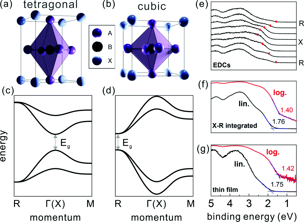 | ||
| Fig. 1 The MHP unit cell of the (a) tetragonal and (b) cubic phase, with the corresponding schematic band structure in (c) and (d), respectively. A, B and X in (a) and (b) represent the halides, bivalent metals and cations, respectively. (e) Energy distribution curves of a MAPbI3 single crystal along the X–R high symmetry direction. Red marks indicate the top VB peak positions. (f) A constructed angle-integrated PES spectrum from the spectra in (e). (g) A common PES spectrum measured on a polycrystalline MAPbI3 thin film. In (f) and (g), the binding energy is given with respect to EF set to zero, and lin./log. indicate the same spectrum plotted on linear/logarithmic intensity scale. Fig. (e–g) are adapted from ref. 11. | ||
With these benchmark band structure data at hand, the global VBM, which is the energy level needed for sketching an energy level diagram, can be reliably accessed. As suggested first by Endres et al.,7 the global VBM (here at the R point) contributes comparably little to angle-integrated PES spectra because of the pronounced dispersion of the topmost valence band (VB). In analogy, a PES spectrum recorded from a polycrystalline MHP thin film comprises contributions from many BZ directions and the signal from the global VBM is weak. For instance, by adding up the angle-resolved spectra from a single crystal in Fig. 1(e) one obtains the spectrum shown in Fig. 1(f), which can serve as model for a spectrum from a polycrystalline film. And indeed, one can observe similarity of the constructed spectrum with that measured on a polycrystalline thin film as shown in Fig. 1(g).11 Traditionally, the VBM is determined from such a spectrum plotted on a linear intensity scale by extrapolation of the leading edge towards the background. This, however, returns an unreasonably large binding energy of the VBM with respect to EF, sometimes even larger than the band gap of the MHP. In contrast, using the same procedure with the data plotted on a logarithmic intensity scale returns a much more accurate value for the VBM. This is expected to be applicable for all MHPs with strongly dispersing topmost VB, so that using a logarithmic intensity scale to evaluate the global VBM position from PES spectra of thin film samples is recommended.7,11
3. Energy level alignment at electrode contacts
Despite substantial amount of work devoted to understand the energy level alignment at perovskite-related surfaces and interfaces, the level alignment with a conductive electrode substrate remained a subject of debate for a long time, and as courteously summarized then by S. Olthof.6 In the Schottky–Mott limit, one would expect for an intrinsic (i.e., undoped) semiconductor that the energy difference between the VBM/conduction band minimum (CBM) and EF of the electrode vary with the substrate work function (Φsub), in the ideal case with a slope of one, where the slope is defined as with Φperovskite being the work function of the perovskite layer on top of the substrate. An alternative phrasing of this phenomenon is that EF moves in the band gap of the MHP as function of Φsub with that slope. If Φsub becomes larger than the IE of the semiconductor, EF would be placed below the VBM. To establish electronic equilibrium, electrons are transferred from the semiconductor to the substrate to form an interface dipole and/or band bending that shifts EF (close) above the VBM and positions the sample work function below the initial Φsub value. This phenomenon is known as intrinsic Fermi level pinning at the band edges (as opposed to Fermi level pinning at gap states), and proceeds in full analogy also at the CBM for Φsub values lower than the semiconductor's EA. Graphically, this can be represented by a plot of the sample's work function after MHP deposition (Φperovskite) as function of Φsub, as shown in Fig. 2(a).
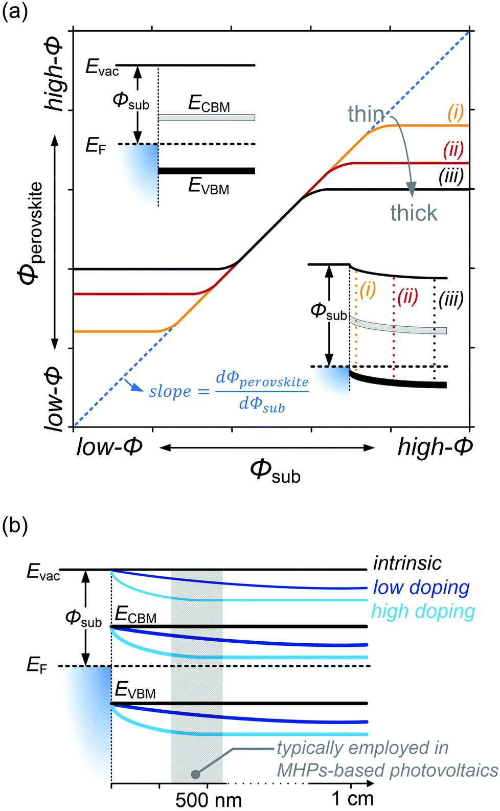 | ||
Fig. 2 (a) Φ of MHP films with different film thicknesses as a function of the substrate work function (Φsub). The insets in (a) depict the vacuum level alignment (top) and Fermi level pinning regimes (bottom). The slope indicated as the dashed blue line is defined as 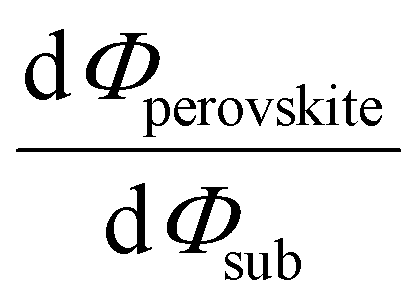 . (b) Schematic energy level diagram of a substrate electrode/MHP interface depending on the doping concentrations. Low doping concentration of ca. 108 cm−3 and high doping concentration of ca. 1017 cm−3. . (b) Schematic energy level diagram of a substrate electrode/MHP interface depending on the doping concentrations. Low doping concentration of ca. 108 cm−3 and high doping concentration of ca. 1017 cm−3. | ||
In that figure, we observe a region where the Schottky–Mott limit – i.e., vacuum level alignment – holds (curves with a slope of 1) and Fermi level pinning at lower and higher Φsub values (slope of zero). The transition between the two regimes is not abrupt because of a finite density of states of the corresponding bands at which pinning occurs. Additionally, the presence of tail states near the band edges32 leads to a more gradual transition. Another observation is that the apparent Φsub at which the transition occurs seemingly depends on the MHP film thickness. This is due to the fact that the charge carriers induced in the semiconductor by the pinning diffuse away from the interface and cause band bending, illustrated by the lower inset in Fig. 2(a) for the case of high Φsub. At different film thickness the magnitude of band bending varies, and in turn the range over which the EF position in the gap appears tunable becomes narrower for larger film thickness. For organic semiconductors the relevant thickness scale was estimated to a few 10 nm,33 but notable band position changes might occur on the 100 nm scale for MHPs because of their much higher dielectric constant (εr). For appropriately prepared MHP thin films, i.e., with suitably low effective doping concentration, the regimes of Schottky–Mott limit and Fermi level pinning – and the transition between them – were observed experimentally.14,34–37
On the contrary, for MHPs with a considerable doping concentration, the range over which EF is free to move can be significantly reduced or even pinned. This can be understood from the consideration that for MHPs with high doping concentration (Nd) of, e.g., 1017 cm−3, the resulting depletion width (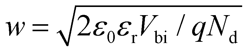 , where ε0, εr and q are the vacuum and relative dielectric constant, and unit electric charge, respectively; Vbi is the built-in voltage given by the work function difference between the substrate and the MHP) of ca. 100 nm is much shorter than the typical film thickness of ca. 500 nm in most experiments. As a result, the surface energy levels are solely controlled by the doping concentration. On the other extreme, the depletion width can extend to ca. 1 mm with a doping concentration of ≤ 108 cm−3. This is exemplified in Fig. 2(b), showing that the EF position measured at the surface of a thin film may not represent the bulk doping level if the film thickness is lower than the depletion width.
It thus appears that the simultaneous actions of the two level alignment regimes and the MHP doping concentration are very challenging to unravel, because possibly counter-acting band bending effects and the pronounced film thickness dependence require a huge set of parameter variations in experiment. Frankly, the sole observation of EF close to the VBM (CBM) for one sample does not imply that the material is p-type (n-type) in the bulk, and the band positions between substrate and film surface may vary considerably.
4. Surface-specific electronic properties
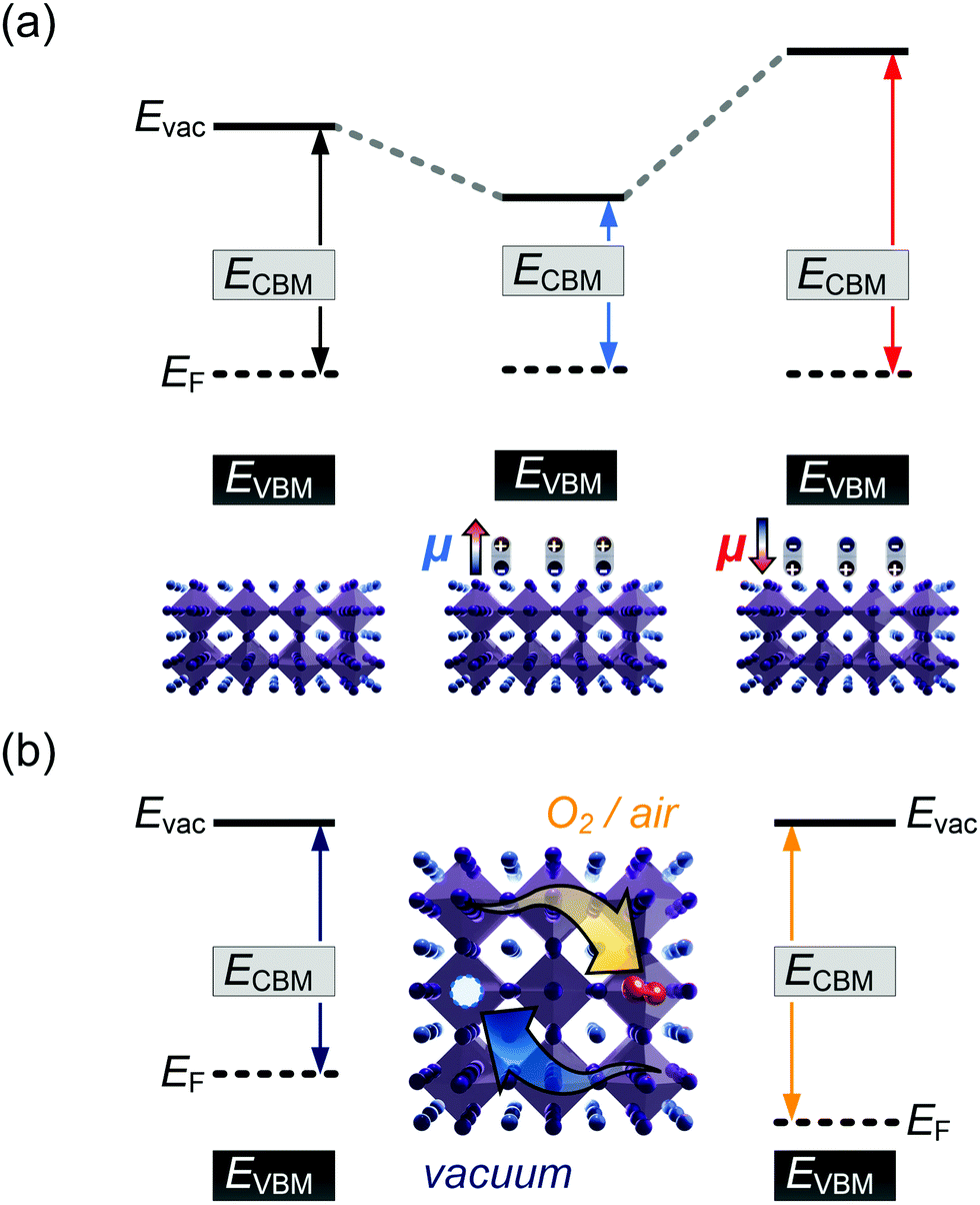
Semiconductor surfaces are often subject to modifications of the electronic properties, distinct from the bulk. This is frequently due to the presence of surface states, which can originate from reconstruction due to dangling bonds at the surface or reactions with adsorbates. Surface states generally exhibit either electron donor (n-type) or acceptor (p-type) character. As a result, near-surface charge rearrangements occur, often leading to a space-charge layer and associated band bending beneath the surface. This has a large impact on the energy levels of the semiconductor surface, and has been widely investigated for traditional semiconductors,38,39 such as GaN40 and ZnO.41 In the presence of donor-type surface states, as schematically shown in Fig. 3, the difference in the EF position between the semiconductor bulk and the surface states drives electrons to redistribute so that electronic equilibrium, i.e., one common alignment of EF, is reached. Consequently, additional electron density builds up in the sub-surface region, accompanied by downward surface band bending, as illustrated in Fig. 3(a). One method to examine the presence of surface band bending is to perform surface photovoltage (SPV) measurements. A simplified picture of the SPV effect is shown in Fig. 3(b). By above band gap optical excitation of the sample, photo-generated electron–holes pairs near the surface dissociate and the carriers are driven in opposite direction by the electric field in the depletion region. Consequently, the accumulation of the photo-induced charge carriers, if recombination is suitably low, produces an electric field that compensates the surface band bending, eventually leading to band flattening at the surface upon sufficiently strong illumination.42 Note that in Fig. 3(b)EF indicates the Fermi level of the conductive substrate on which the MHP film resides, and that under illumination the carrier distribution should be described by the quasi-Fermi levels for electrons and holes; these are, however, not accessible from PES measurements. The SPV phenomenon was repeatedly observed for various MHPs.12,43–45 For apparently n-type MHPs (i.e., EF at the surface close to the CBM), from PES and Kelvin probe measurement under varied optical excitation intensities, EF was found to shift by up 0.8 eV towards approximately mid-gap due to the SPV effect. This evidenced that the samples were not n-type in the bulk, and that the strong n-type character of the surface could be attributed to the presence of donor-type surface states, assigned to Pb0 species.9,12 It is important to note that even the vacuum ultraviolet (VUV) light as typically used in PES experiments to excite the photoelectrons can induce a large SPV, giving rise to a measurement of the energy levels in a non-equilibrium condition of the surface.12 Therefore, in order to approach the equilibrium electronic properties of MHPs by PES measurements, it is highly recommended to always carefully check for SPV effects by both, variation of optical and VUV irradiation intensities of the sample.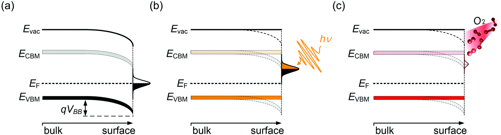 | ||
| Fig. 3 Schematic energy diagrams of the surface band bending situations induced by donor-type surface states (a) at the electronic ground state, (b) non-equilibrium state under photo-excitation, i.e., band flattening due to SPV effect and (c) upon O2 exposure, i.e., the O2 passivation effect on the Pb0-related surface states. | ||
The Pb0-related surface states can be created on purpose by illumination of a MHP sample with visible light in vacuum, up to such a high dosage that metallic Pb clusters form.9 In this light-induced degradation process, organic cations and halides as volatile species leave and residual solid PbI2 and metallic Pb remain on the sample surface. Upon oxygen exposure, Pb0 is oxidized and the these electronic defects become passivated,14,46 which is also observed as a recovery of the photoluminescence quantum yield of Pb0-defective MHPs films upon oxygen exposure.47 The photo-induced decomposition of MHPs in vacuum can be significantly suppressed when the surface is covered with a thin inert layer, e.g., of a molecular or polymeric insulator, because this keeps the reaction products in close proximity so that the rather effective back-reaction to the original perovskite can occur.15
5. Environmental effects on the energy levels
It is further of importance to take into account possible environmental effect on the electronic structure of MHPs, as this is highly relevant not only for practical film fabrication but also for many characterization methods. For instance, MHPs films are typically made with solution-processes that involve solvents, and impurities (e.g., water and oxygen molecules) may readily be introduced. If samples are exposed to air, one must further consider gas diffusion into the material and various adsorbates, which can impact IE, EA, and Φ of the sample. Regarding the latter, Fig. 4(a) depicts the situation where polar surface adsorbates are present. These possess a permanent dipole moment, which is the case for water and many solvent molecules, and if they assemble with a preferred orientation with respect to the surface, a surface dipole will result. This surface dipole induces a change of the sample work function (ΔΦ) according to the Helmholtz equation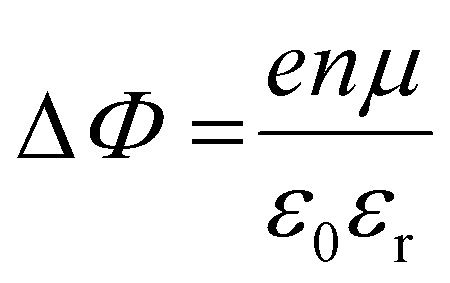 , where n, e and μ are the molecule area density, the elementary charge, and the molecular dipole moment component perpendicular to the surface. For instance, it was shown that water molecules adsorbed on a MHP surface decreased the sample work function by 100 meV. The bulk electronic states of the sample are not influenced by the adsorbate, i.e., the position of EF with respect to the band edges does not change. But ΔΦ affects the IE/EA values because they are defined as energy difference between the VBM/CBM and the vacuum level (Evac), as can be seen from Fig. 4(a) for the two possible opposite preferred dipole orientations. Water adsorption is reversible, and the molecules desorb readily at room temperature in high vacuum, implying physisorption on the MHPs surface.46 The use of dipolar molecular layers or ionic liquids at the surface of MHPs to tune their Φ and thus the energy level alignment with subsequently deposited charge transport layers was shown to be beneficial for solar cells.48–50 Another approach, often termed surface transfer doping, allows for even larger ΔΦ of MHP surfaces. It comprises the use of strong molecular acceptors or donors deposited on the surface, so that ground state charge transfer occurs, which also induces an interface dipole and thus modifies Φ.51–53
 | ||
| Fig. 4 Schematic representation of the impact of (a) an adsorbate-induced surface dipole, and (b) O2 diffusion and doping on the energy levels of MHPs. (a) Molecules with opposite dipole moment μ orientation on the MHP surface lead to a decrease or increase of the work function (indicated by the colored arrows) by the respective ΔΦ. Evac is the vacuum level. (b) Reversible O2-doping by exposing the MHP to O2 and vacuum consecutively, resulting in a shift of the EF position within the band gap. | ||
A different important process changes the majority charge carrier type and density, as well as Φ of a MHP, but leaves IE and EA unaffected: doping. Aside from intentionally introduced dopants in the bulk of MHPs, oxygen can diffuse into and out of MHP thin films, at least those containing organic cations.14,54 Starting from an intrinsic MHP sample with EF about mid-gap, O2 exposure leads to a shift of EF towards the VBM over the course of several 10 min., i.e., the sample becomes p-doped. Bringing this sample into (ultrahigh) vacuum leads to O2 out-diffusion and the MHP returns intrinsic, but on a long time scale of several hours at room temperature. In conjunction with DFT calculations, it was suggested that O2 molecules occupy iodine vacancy sites, resulting in the p-type doping effect.14,54,55 Apparently, oxygen-induced p-doping is reversible but features rather long characteristic timescales. Consequently, one should bear in mind that experiments performed on organic cation containing MHPs in air most likely return information about a rather strongly p-type doped material. It should thus be worthwhile to enforce experiments – particularly including optical methods – to be performed in inert atmosphere or ultrahigh vacuum, despite the admittedly more involved apparatuses and procedures.
6. Summary and outlook
Metal halide perovskites are semiconductors that exhibit the rich electronic phenomena known from their more established counterparts, such as interface- and dopant-induced band bending, surface states and surface band bending, and surface photovoltage. But they feature even more complexity due to moderate stability under optical excitation in vacuum that can induce surface states, and reversible p-doping by (ambient) oxygen. The simultaneous occurrence of all these phenomena has initially retarded progress towards a comprehensive understanding of their electronic properties. Now that several important fundamental questions are resolved, such as those described here, we can look forward to obtaining deeper insight into even more complex properties and processes of this fascinating material class. This, however, necessitates designing and performing experiments with careful consideration of all intrinsic and extrinsic factors that are known to influence the electronic (and thus also optoelectronic) properties of MHPs.For instance, the electronic band structure of the presently widely used mixed-cation and mixed-halide perovskites is still to be uncovered theoretically and experimentally. Also the impact of carrier-lattice coupling on the electronic structure has barely been explored, at least in experiment. A more elaborate knowledge about the atomistic surface structure is needed, particularly for thin films and in vacuum. The latter two aspects are critically important for improved device design that is based on interfacial energy level management. The most direct manner to assess energy levels is the use of photoelectron spectroscopy, which is done in vacuum. Any structural change after interface formation can also alter the MHP electronic properties – and thus the level alignment. To lessen the constraints of performing PES measurements in ultrahigh vacuum, it will be interesting to see increasing activity with near-ambient pressure ultraviolet and X-ray PES, which might result in higher confidence in correlating interfacial energy levels and device performance. We hope that our article motivates and helps researchers to tackle the challenges on the way towards an indeed comprehensive understanding of MHP electronic properties.
Conflicts of interest
There are no conflicts of interest to declare.Acknowledgements
This work was funded by the Deutsche Forschungsgemeinschaft (DFG, German Research Foundation, Project numbers 182087777-SFB951 and 423749265-SPP2196 “SURPRISE”). We thank David Egger and Leeor Kronik for sharing their computed band structure data.References
- J.-H. Im, C.-R. Lee, J.-W. Lee, S.-W. Park and N.-G. Park, Nanoscale, 2011, 3, 4088–4093 RSC.
- L. Dou, Y. Yang, J. You, Z. Hong, W.-H. Chang, G. Li and Y. Yang, Nat. Commun., 2014, 5, 5404 CrossRef CAS.
- Z. K. Tan, R. S. Moghaddam, M. L. Lai, P. Docampo, R. Higler, F. Deschler, M. Price, A. Sadhanala, L. M. Pazos, D. Credgington, F. Hanusch, T. Bein, H. J. Snaith and R. H. Friend, Nat. Nanotechnol., 2014, 9, 687–692 CrossRef CAS.
- H. Zhu, Y. Fu, F. Meng, X. Wu, Z. Gong, Q. Ding, M. V. Gustafsson, M. T. Trinh, S. Jin and X. Y. Zhu, Nat. Mater., 2015, 14, 636–642 CrossRef CAS.
- M. Jeong, I. W. Choi, E. M. Go, Y. Cho, M. Kim, B. Lee, S. Jeong, Y. Jo, H. W. Choi, J. Lee, J.-H. Bae, S. K. Kwak, D. S. Kim and C. Yang, Science, 2020, 369, 1615–1620 CrossRef CAS.
- S. Olthof, APL Mater., 2016, 4, 091502 CrossRef.
- J. Endres, D. A. Egger, M. Kulbak, R. A. Kerner, L. Zhao, S. H. Silver, G. Hodes, B. P. Rand, D. Cahen, L. Kronik and A. Kahn, J. Phys. Chem. Lett., 2016, 7, 2722–2729 CrossRef CAS.
- F. Zu, P. Amsalem, M. Ralaiarisoa, T. Schultz, R. Schlesinger and N. Koch, ACS Appl. Mater. Interfaces, 2017, 9, 41546–41552 CrossRef CAS.
- F.-S. Zu, P. Amsalem, I. Salzmann, R.-B. Wang, M. Ralaiarisoa, S. Kowarik, S. Duhm and N. Koch, Adv. Opt. Mater., 2017, 5, 1700139 CrossRef.
- F. Zhang, F. Ullrich, S. Silver, R. A. Kerner, B. P. Rand and A. Kahn, J. Phys. Chem. Lett., 2019, 10, 890–896 CrossRef CAS.
- F. Zu, P. Amsalem, D. A. Egger, R. Wang, C. M. Wolff, H. Fang, M. A. Loi, D. Neher, L. Kronik, S. Duhm and N. Koch, J. Phys. Chem. Lett., 2019, 10, 601–609 CrossRef.
- F. Zu, C. M. Wolff, M. Ralaiarisoa, P. Amsalem, D. Neher and N. Koch, ACS Appl. Mater. Interfaces, 2019, 11, 21578–21583 CrossRef CAS.
- L. Qiu, S. He, L. K. Ono and Y. Qi, Adv. Energy Mater., 2020, 10, 1902726 CrossRef CAS.
- D. Shin, F. Zu, A. V. Cohen, Y. Yi, L. Kronik and N. Koch, Adv. Mater., 2021, 33, 2100211 CrossRef CAS.
- F. Zu, T. Schultz, C. M. Wolff, D. Shin, L. Frohloff, D. Neher, P. Amsalem and N. Koch, RSC Adv., 2020, 10, 17534–17542 RSC.
- X. Tang, M. Brandl, B. May, I. Levchuk, Y. Hou, M. Richter, H. Chen, S. Chen, S. Kahmann, A. Osvet, F. Maier, H.-P. Steinrück, R. Hock, G. J. Matt and C. J. Brabec, J. Mater. Chem. A, 2016, 4, 15896–15903 RSC.
- T. Baikie, Y. Fang, J. M. Kadro, M. Schreyer, F. Wei, S. G. Mhaisalkar, M. Graetzel and T. J. White, J. Mater. Chem. A, 2013, 1, 5628–5641 RSC.
- M. T. Weller, O. J. Weber, P. F. Henry, A. M. Di Pumpo and T. C. Hansen, Chem. Commun., 2015, 51, 4180–4183 RSC.
- P. S. Whitfield, N. Herron, W. E. Guise, K. Page, Y. Q. Cheng, I. Milas and M. K. Crawford, Sci. Rep., 2016, 6, 35685 CrossRef CAS.
- T. W. Kim, S. Uchida, T. Matsushita, L. Cojocaru, R. Jono, K. Kimura, D. Matsubara, M. Shirai, K. Ito, H. Matsumoto, T. Kondo and H. Segawa, Adv. Mater., 2018, 30, 1705230 CrossRef.
- E. Menéndez-Proupin, P. Palacios, P. Wahnón and J. C. Conesa, Phys. Rev. B: Condens. Matter Mater. Phys., 2014, 90, 045207 CrossRef.
- P. Umari, E. Mosconi and F. De Angelis, Sci. Rep., 2014, 4, 4467 CrossRef.
- J. Even, L. Pedesseau, C. Katan, M. Kepenekian, J.-S. Lauret, D. Sapori and E. Deleporte, J. Phys. Chem. C, 2015, 119, 10161–10177 CrossRef CAS.
- Y. H. Chang, C. H. Park and K. Matsuishi, J. Korean Phys. Soc., 2004, 44, 889–893 CAS.
- W. G. Aulbur, L. Jönsson and J. W. Wilkins, in Solid State Phys., ed. H. Ehrenreich and F. Spaepen, Academic Press, 2000, vol. 54, pp. 1–218 Search PubMed.
- J. Even, L. Pedesseau, J.-M. Jancu and C. Katan, J. Phys. Chem. C, 2013, 4, 2999–3005 CAS.
- H. Beck, C. Gehrmann and D. A. Egger, APL Mater., 2019, 7, 021108 CrossRef.
- J. Shi and S. Yun, in Counter Electrodes for Dye-sensitized and Perovskite Solar Cells, II, ed. S. Yun and A. Hagfeldt, Wiley-VCH Verlag GmbH & Co. KGaA, 2018, ch. 19, pp. 487–509 Search PubMed.
- W. Zhang, Photoemission Spectroscopy on High Temperature Superconductor, Springer, 2013 Search PubMed.
- Y. Nakayama, S. Kera and N. Ueno, J. Mater. Chem. C, 2020, 8, 9090–9132 RSC.
- J. Yang, H. Sato, H. Orio, X. Liu, M. Fahlman, N. Ueno, H. Yoshida, T. Yamada and S. Kera, J. Phys. Chem. Lett., 2021, 12, 3773–3778 CrossRef CAS.
- F. Zhang, J. C. Hamill Jr., Y.-L. Loo and A. Kahn, Adv. Mater., 2020, 32, 2003482 CrossRef CAS.
- M. Oehzelt, N. Koch and G. Heimel, Nat. Commun., 2014, 5, 4174 CrossRef CAS.
- P. Schulz, L. L. Whittaker-Brooks, B. A. MacLeod, D. C. Olson, Y.-L. Loo and A. Kahn, Adv. Mater. Interfaces, 2015, 2, 1400532 CrossRef.
- A. Zohar, M. Kulbak, I. Levine, G. Hodes, A. Kahn and D. Cahen, ACS Energy Lett., 2018, 4, 1–7 Search PubMed.
- S. Olthof and K. Meerholz, Sci. Rep., 2017, 7, 40267 CrossRef CAS.
- E. M. Miller, Y. Zhao, C. C. Mercado, S. K. Saha, J. M. Luther, K. Zhu, V. Stevanovic, C. L. Perkins and J. van de Lagemaat, Phys. Chem. Chem. Phys., 2014, 16, 22122–22130 RSC.
- W. Mönch, Semiconductor Surfaces and Interfaces, Springer, 1993 Search PubMed.
- S. G. Davison and J. D. Levine, in Solid State Phys., ed. H. Ehrenreich, F. Seitz and D. Turnbull, Academic Press, 1970, vol. 25, pp. 1–149 Search PubMed.
- T. Schultz, R. Schlesinger, J. Niederhausen, F. Henneberger, S. Sadofev, S. Blumstengel, A. Vollmer, F. Bussolotti, J. P. Yang, S. Kera, K. Parvez, N. Ueno, K. Müllen and N. Koch, Phys. Rev. B, 2016, 93, 125309 CrossRef.
- M. Valtiner, M. Todorova and J. Neugebauer, Phys. Rev. B: Condens. Matter Mater. Phys., 2010, 82, 165418 CrossRef.
- L. Kronik and Y. Shapira, Surf. Sci. Rep., 1999, 37, 1–206 CrossRef CAS.
- L. Barnea-Nehoshtan, S. Kirmayer, E. Edri, G. Hodes and D. Cahen, J. Phys. Chem. Lett., 2014, 5, 2408–2413 CrossRef CAS.
- J. R. Harwell, T. K. Baikie, I. D. Baikie, J. L. Payne, C. Ni, J. T. Irvine, G. A. Turnbull and I. D. Samuel, Phys. Chem. Chem. Phys., 2016, 18, 19738–19745 RSC.
- M. Daboczi, I. Hamilton, S. Xu, J. Luke, S. Limbu, J. Lee, M. A. McLachlan, K. Lee, J. R. Durrant, I. D. Baikie and J.-S. Kim, ACS Appl. Mater. Interfaces, 2019, 11, 46808–46817 CrossRef CAS.
- M. Ralaiarisoa, I. Salzmann, F.-S. Zu and N. Koch, Adv. Electron. Mater., 2018, 4, 1800307 CrossRef.
- S. G. Motti, M. Gandini, A. J. Barker, J. M. Ball, A. R. Srimath Kandada and A. Petrozza, ACS Energy Lett., 2016, 1, 726–730 CrossRef CAS.
- S. Xiong, Y. Dai, J. Yang, W. Xiao, D. Li, X. Liu, L. Ding, P. Gao, M. Fahlman and Q. Bao, Nano Energy, 2021, 79, 105505 CrossRef CAS.
- P. Caprioglio, D. S. Cruz, S. Caicedo-Dávila, F. Zu, A. A. Sutanto, F. Peña-Camargo, L. Kegelmann, D. Meggiolaro, L. Gregori, C. M. Wolff, B. Stiller, L. Perdigón-Toro, H. Köbler, B. Li, E. Gutierrez-Partida, I. Lauermann, A. Abate, N. Koch, F. De Angelis, B. Rech, G. Grancini, D. Abou-Ras, M. K. Nazeeruddin, M. Stolterfoht, S. Albrecht, M. Antonietti and D. Neher, Energy Environ. Sci., 2021, 14, 4508–4522 RSC.
- C. M. Wolff, L. Canil, C. Rehermann, N. Ngoc Linh, F. Zu, M. Ralaiarisoa, P. Caprioglio, L. Fiedler, M. Stolterfoht, S. Kogikoski, I. Bald, N. Koch, E. L. Unger, T. Dittrich, A. Abate and D. Neher, ACS Nano, 2020, 14, 1445–1456 CrossRef CAS.
- N. K. Noel, S. N. Habisreutinger, A. Pellaroque, F. Pulvirenti, B. Wenger, F. Zhang, Y.-H. Lin, O. G. Reid, J. Leisen, Y. Zhang, S. Barlow, S. R. Marder, A. Kahn, H. J. Snaith, C. B. Arnold and B. P. Rand, Energy Environ. Sci., 2019, 12, 3063–3073 RSC.
- J. Euvrard, O. Gunawan, X. Zhong, S. P. Harvey, A. Kahn and D. B. Mitzi, Mater. Adv., 2021, 2, 2956–2965 RSC.
- E. E. Perry, J. G. Labram, N. R. Venkatesan, H. Nakayama and M. L. Chabinyc, Adv. Electron. Mater., 2018, 4, 1800087 CrossRef.
- D. Shin, F. Zu and N. Koch, APL Mater., 2021, 9, 081104 CrossRef CAS.
- D. Meggiolaro, E. Mosconi and F. De Angelis, ACS Energy Lett., 2017, 2, 2794–2798 CrossRef CAS.
| This journal is © The Royal Society of Chemistry 2022 |