
 Open Access Article
 This Open Access Article is licensed under a Creative Commons Attribution-Non Commercial 3.0 Unported Licence
Tuning of hole carrier density in p-type α-SnWO4 by exploiting oxygen defects†
Makoto
Minohara
 *a,
Yuka
Dobashi
ab,
Naoto
Kikuchi
a,
Akane
Samizo
b,
Takashi
Honda
cd,
Xinyi
He
e,
Takayoshi
Katase
e,
Toshio
Kamiya
e,
Keishi
Nishio
b and
Yoshihiro
Aiura
a
*a,
Yuka
Dobashi
ab,
Naoto
Kikuchi
a,
Akane
Samizo
b,
Takashi
Honda
cd,
Xinyi
He
e,
Takayoshi
Katase
e,
Toshio
Kamiya
e,
Keishi
Nishio
b and
Yoshihiro
Aiura
a
aResearch Institute for Advanced Electronics and Photonics, National Institute of Advanced Industrial Science and Technology (AIST), Tsukuba, Ibaraki 305-8568, Japan. E-mail: m-minohara@aist.go.jp; Tel: +81-29-862-6475
bDepartment of Materials Science and Technology, Tokyo University of Science, Katsushika, Tokyo 125-8585, Japan
cMaterials & Life Science Division, J-PARC Centre, Tokai, Ibaraki 319-1195, Japan
dInstitute of Materials Structure Science, High Energy Accelerator Research Organization (KEK), Tsukuba, Ibaraki 305-0801, Japan
eLaboratory for Materials and Structures, Institute of Innovative Research, Tokyo Institute of Technology, 4259 Nagatsuta, Midori, Yokohama 226-8503, Japan
First published on 8th November 2022
Abstract
The development of p-type oxide semiconductors has shown promise in overcoming limitations restricting the practical usage of oxide semiconductors and the realization of innovative functional devices. Through numerous studies based on both experimental and theoretical approaches, several state-of-the-art p-type oxide semiconductors have been discovered. However, one of the challenges concerning these p-type oxide semiconductors is on tuning the hole carrier density. In this study, precise tuning of the hole carrier density in α-SnWO4 based on thermodynamic condition control was demonstrated. A detailed investigation of the crystal structure via X-ray diffraction, extended X-ray absorption fine structures, and density functional theory calculations revealed the role of oxygen defects, such as oxygen vacancies and interstitials, in tuning the hole carrier density. This study shows the importance of fine-tuning of oxygen defects based on thermodynamic condition control for the emergence and improvement of p-type semiconducting properties in Sn2+-based oxides.
Introduction
Wide-bandgap oxide semiconductors, such as ZnO, In2O3, and Ga2O3, are promising materials for the development of innovative (opto-)electronic devices based on their transparency and high breakdown voltage.1 However, because of the characteristic electronic configurations of their valence bands, these wide-bandgap oxide semiconductors are mostly of the n-carrier type, and consequently, the potential of these semiconductors for practical application is presently limited. One of the strategies to overcome this limitation is the development of p-type oxide semiconductors via the modulation of the valence band.2–6Based on an analogy with the amorphous n-type oxide semiconductors InGaZnO4 and Sn-doped In2O3, oxide semiconductors with ns2 (n ≥ 5) orbitals in their valence band maxima (VBM) are expected to have small effective masses for holes because of the dispersive band edges and high tolerance features for structural disordering arising from their spatially spreading orbitals.7,8 Indeed, SnO films with VBMs comprising the Sn 5s2 orbital exhibit negligible differences in hole mobility between epitaxially grown and polycrystalline structures. However, the growth conditions required to obtain the highest mobility of 18–20 cm2 V−1 s−1 for SnO are considerably limited because of its chemical instability.3,9–11
Recently, several p-type oxide semiconductors with ns2 orbitals have been developed based on predictions through theoretical approaches.12–17 These state-of-the-art p-type oxide semiconductors can be categorized into two groups: one is for Sn2+-based oxide semiconductors, such as pyrochlore-type Sn2TM2O7 (TM = Nb or Ta)13 and layered-structure SnNb2O6 and α-SnWO4;14,15 and the other is for Bi3+-based oxide semiconductors, such as perovskite-type BaBiO3,16 double-perovskite-type Ba2BiTMO6,12,16 and pyrochlore-type Bi2Sn2O7.17 Of the two, Sn2+-based oxide semiconductors are less chemically stable than Bi3+-based ones because of their metastable Sn2+ states. However, this disadvantage is expected to be overcome via the selection of an appropriate crystal structure based on phase stability.18 On the other hand, the hole carrier densities of Sn2+-based oxide semiconductors (1017–1018 cm−3) are several orders of magnitude greater than those of Bi3+-based ones (1013–1014 cm−3).12–17 Such characteristics of Sn2+-based oxide semiconductors in terms of carrier density are useful for designing electronic devices with high conductivities.
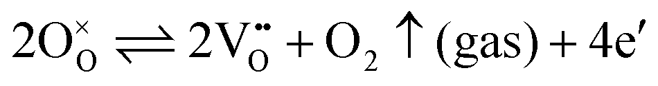
In this regard, precise tuning of the carrier densities of Sn2+-based p-type oxide semiconductors is highly necessary. However, intentional control over the hole carrier density remains a challenging undertaking.17,19–22 Especially, Sn2+-based oxides in the thin-film form still show the insulating properties.19–22 This is likely because oxygen vacancies form spontaneously to compensate for the positive charge.19,20,23 For example, in α-SnWO4, the net hole carrier density is determined by a balance between the following defect formations, as shown by this Kröger–Vink notation:
 | (1) |
 | (2) |
 and
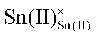
and  are Sn2+ at the original Sn site and O2− at the original O site, respectively; and
  is the oxygen vacancy. Here, we assume the formation of an additional sublattice composed of
 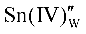 and
and 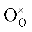 , as previously reported.24
 is the Sn4+ substitutional defect at the W6+ site, and
  corresponds not to the tin vacancy due to evaporation from the material but to the resultant void due to the formation of
  .15,24 Meanwhile,
  and e′ denote the holes and electrons, respectively. As a result, the hole carrier generation efficiencies of Sn2+-based oxide semiconductors from Sn4+ substitutional defects are tremendously low, as low as 0.005–1.4%; the efficiencies of layered-structure Sn2+-based oxide semiconductors are much greater than that of pyrochlore-type ones.13,14,24 This is due to electrostatic interaction between electron densities at Sn2+ ions and surrounded O2− ions.24 Therefore, the layered-structure Sn2+-based oxide semiconductors should be promising materials showing high hole carrier densities.
Here, it can be expected that the net hole carrier density would increase at oxidizing conditions because the numbers of holes and electrons are increased and decreased, respectively, based on eqn (1) and (2), respectively. On the other hand, the optimum conditions may be limited by the metastable Sn2+ valence state and the valence-fluctuating nature of transition metal ions. Prior to investigating the conditions for emerging the p-type conductivity of Sn2+-based oxide films, it is essential that precise information on the manipulation of oxygen defects in those bulk forms with the p-type conductivities.14,15 In this study, we demonstrate that precise control over the O2 gas concentration during the annealing process is effective for tuning the hole carrier density of α-SnWO4. The hole carrier density increased by two orders of magnitude and achieved a value close to 1019 cm−3, which is comparable with the highest carrier density of SnO,3 at an optimum O2 gas concentration.
Experimental section
Synthesis
Samples of α-SnWO4 were synthesized via a solid-state reaction. Here, SnO (Kojundo Chemical Laboratory; purity 99.5%) and WO3 (Kojundo Chemical Laboratory; purity 99.9%) were mixed in an agate mortar with ethanol, after which the mixed powders were dried in air for 24 h and then calcined at 600 °C in a tube furnace under N2 at a flow rate of 150 ml min−1. At this point, the synthesis of α-SnWO4 samples was completed. After synthesis, 2 wt% polyvinyl alcohol aqueous solution was added, and the mixture was stirred for 15 min, which was followed by sieving to obtain narrow sieve fractions of <212 μm. The obtained powder was pressed uniaxially at 270 MPa and then isostatically at 290 MPa to form tablets with a diameter of 12 mm and thickness of 1 mm. The samples were annealed at 650 °C in a tube furnace under an N2/O2 gas mixture at a total flow rate of 50 ml min−1. The concentration of O2 gas was controlled to be within the range 0–100 ppm via the ratio of the flow rates of the N2 and O2 gases.Characterization
The chemical compositions of the samples were determined using a wavelength-dispersive X-ray fluorescence (XRF) spectrometer (Rigaku ZSX). Diffuse reflectance spectra were measured using a double-beam ultraviolet-visible spectrometer with an integrating sphere (Shimadzu UV-2550) and converted into absorption spectra using the Kubelka–Munk method. The carrier types of the α-SnWO4 samples were determined based on the sign of the Hall and Seebeck coefficients (measured using the Resitest 8310 (Toyo Corp.) and ZEM-3 (ADVANCE RIKO Inc.) measurement systems, respectively).The crystal structure and lattice parameters were analyzed via X-ray diffraction (XRD) using the Bragg–Brentano configuration with Cu Kα radiation (PANalytical, X’Pert Pro MPD) and synchrotron-based XRD (SR-XRD), which was performed at beamline BL-8B at the Photon Factory (PF), KEK. The energy of the incident synchrotron-based X-rays was 18 keV. The structural parameters were refined via Rietveld analysis using Z-Rietveld ver. 1.1.11,25,26 and crystal structures were drawn using VESTA.27 The local crystal structures were investigated using extended X-ray absorption fine structure (EXAFS) measurements at 40 K. Sn K- and W L3-edge EXAFS measurements in the transmission mode were acquired at beamline AR-NW10A28 of the KEK PF Advanced Ring and at BL-9A of the PF, respectively. The EXAFS spectra were Fourier transformed using the Hanning window function within a k range of 3–17 Å for both the Sn K- and W L3-edges. The EXAFS spectra were processed using Athena.29
Density functional theory (DFT) calculation
DFT calculations for α-SnWO4 were conducted using the projector augmented wave (PAW) method implemented in the Vienna Ab initio Simulation Package (VASP).30,31 Sn [4d5s5p], W [5s5p5d6s], and O [2s2p] were included as valence states. The O vacancy and interstitial defect models (SnWO3.75 and SnWO4.25) were built based on the removal or addition of one O atom from or to a fully relaxed α-SnWO4 unit cell (four Sn atoms, four W atoms, and 16 O atoms). All variable-cell structure relaxations were performed using the generalized gradient approximation (GGA) Perdew–Burke–Ernzerhof revised for solids (PBEsol) functional32 with a plane wave cut-off energy of 550 eV and a gamma-centered k-spacing of 0.1 Å−1. The internal atomic coordinates were fully relaxed until the total energy difference was smaller than 10−6 eV and all the forces on the atoms became less than 0.01 eV Å−1.Results and discussion
XRD measurements were performed to investigate the effect of annealing on the crystal structures of the α-SnWO4 samples. Fig. 1 shows the XRD 2θ–θ patterns for the α-SnWO4 samples after annealing at O2 gas concentrations of 0–100 ppm. The observed XRD patterns well describe the single-phase α-SnWO4; the annealed samples are free from any side effects, such as the generation of impurity phases or disproportionation to Sn metal and Sn4+ compounds. When the O2 gas concentration was 0.4%, the sample was completely decomposed into SnO2 and WO3.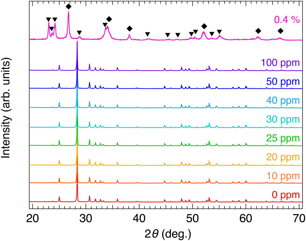 | ||
| Fig. 1 2θ–θ X-ray diffraction patterns of α-SnWO4 samples for different O2 gas concentrations during annealing after synthesis. Triangles and diamonds in the XRD pattern of 0.4% sample correspond to the decomposed WO3 and SnO2, respectively. | ||
Fig. 2 shows the carrier densities of α-SnWO4 samples annealed at different O2 gas concentrations after synthesis. The Seebeck coefficients were positive for all samples (Fig. S1, ESI†), indicating a p-carrier type (holes) conduction. From 0 to 30 ppm, the carrier density increased monotonically from 7 × 1016 cm−3 to 8 × 1018 cm−3. The high carrier densities have been maintained one year after the initial characterization. When the O2 gas concentration was ≥40 ppm, the carrier density decreased until it was maintained at a final value of 6 × 1017 cm−3. While the carrier density changed as a function of the O2 gas concentration, the optical band gap changed only negligibly (Fig. S2, ESI†).
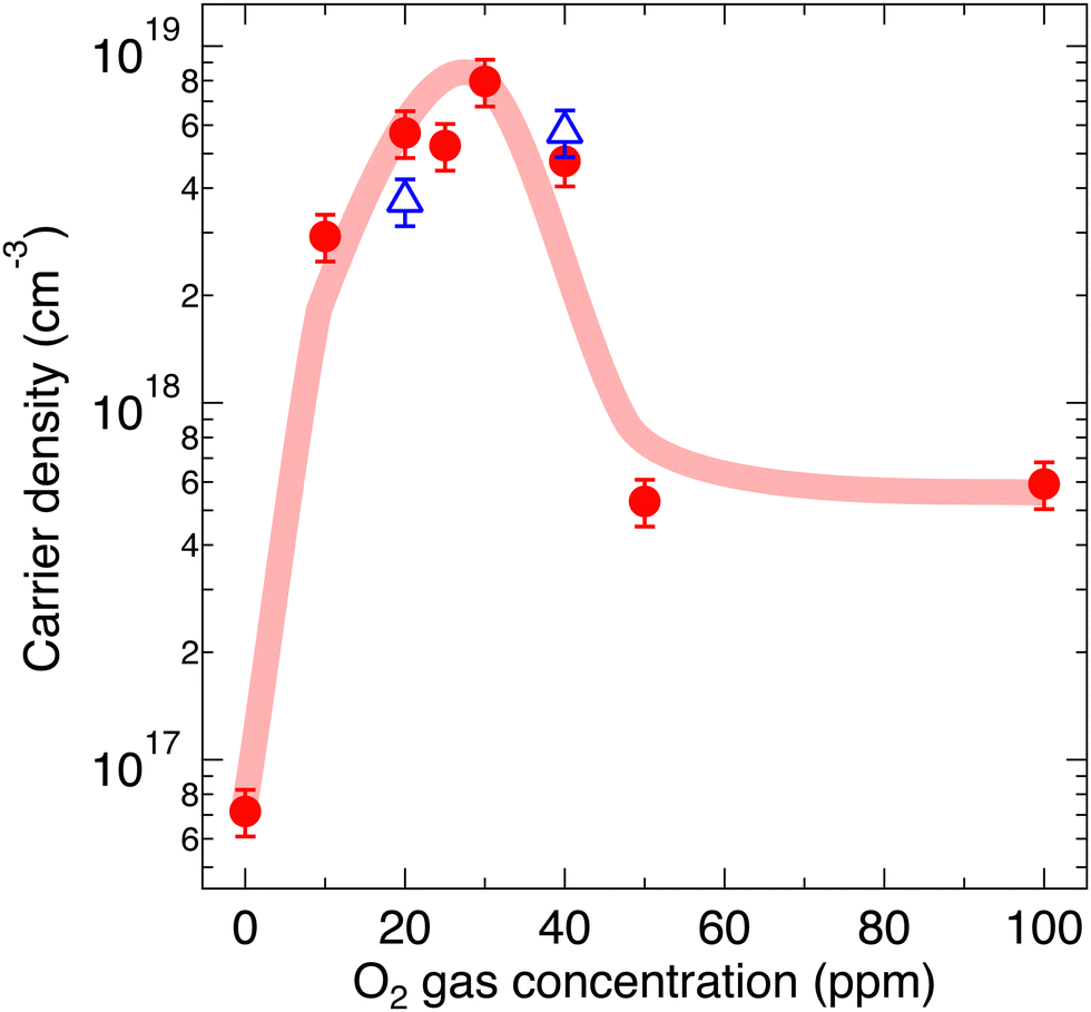 | ||
| Fig. 2 Carrier densities at room temperature of α-SnWO4 samples as function of O2 gas concentration. The solid line is guide. Triangles correspond to the data measured one year after the initial measurements (circles). | ||
The former trend can be explained by the suppression of  formation; however, the latter cannot be explained by the expected defect formation (eqn (1) and (2)). To clarify the mechanism of the carrier density changes, we investigated the crystal structure change. Plots of the unit-cell volume as a function of the O2 gas concentration during annealing are shown in Fig. 3. Here, the unit-cell volume was estimated based on the lattice constants of a, b, and c axes obtained through Rietveld analyses of the XRD 2θ–θ patterns (Fig. S3, ESI†). As the O2 gas concentration increased, the unit-cell volume decreased when the O2 gas concentration was ≤30 ppm, whereas the unit-cell volume increased when the O2 gas concentration was ≥40 ppm. This result suggests that the observed trend for the carrier density (Fig. 2) originates from the unit-cell volume and associated local structure changes (Fig. 3).
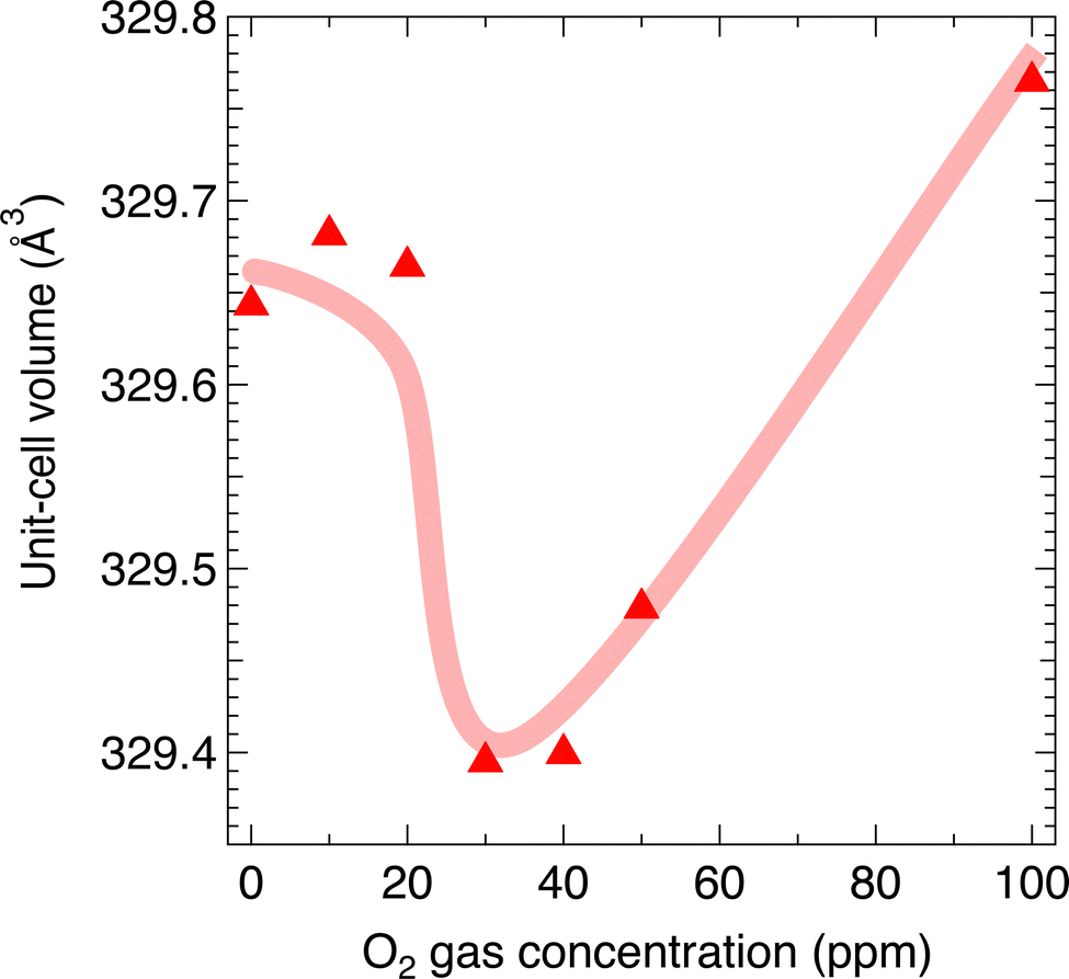 | ||
| Fig. 3 Plots of unit-cell volume obtained through Rietveld analysis of 2θ–θ X-ray diffraction patterns of α-SnWO4 samples as function of O2 gas concentration. The solid line is guide. | ||
Based on a unit-cell volume of 326.46 Å3 for the ideal α-SnWO4 obtained via our DFT calculation, the decrease in unit-cell volume for the samples annealed at O2 gas concentrations in the range 0–30 ppm is most likely explained by the suppression of  formation.33 By contrast, the increase in unit-cell volume at above 40 ppm cannot be naturally explained by
  regeneration at higher O2 gas concentrations. Cation non-stoichiometry in complex oxides is well known to be a possible cause of lattice expansion;34 however, a nearly stoichiometric Sn/W ratio was confirmed via XRF measurements for all samples (Fig. S4, ESI†). At this point, what remains to be analyzed is the possibility of interstitial oxygen defects (Oi).35 α-SnWO4 is composed of an alternating structure of WO6 octahedra and Sn2+ layers, and thus it is inferred that repulsions between lone-pair electrons will create a rather large space in the crystal structure. Therefore, it is expected that Oi can be formed around the Sn2+ ions.
Our DFT calculations confirmed these inferences, namely, on the expansion of the unit-cell volume by  or Oi formation. The α-SnWO4 contains oxygen ions of two types; four O2− ions (O(1)), each connected to a nearest-neighbor WO6 octahedron, and O2− ion pairs (O(2)) supporting the Sn2+ layer (Fig. 4A). In the case of p-type α-SnWO4,
  is preferentially formed at the O(2) site.15 The unit-cell volume of α-SnWO4 with
  at the O(2) site was calculated to be 330.65 Å3 indicating the expansion of the unit-cell volume. On the other hand, to determine the effects of Oi formation, the unit-cell volumes were calculated for six models with different Oi site (Fig. 4A–F). The calculated values of unit-cell volume with respect to Oi formation are shown in Fig. 4G. These six models can be categorized into three groups based on the following criteria: Oi formation on the Sn2+ layer (A and B), Oi formation on the WO6 octahedral layer (E and F), and Oi formation between the Sn2+ and WO6 octahedral layers (C and D). Of these, cases A to D exhibited unit-cell volume expansion. Therefore, α-SnWO4 annealed at higher oxygen concentrations (e.g., 100 ppm) may have Oi around the Sn2+ ions.
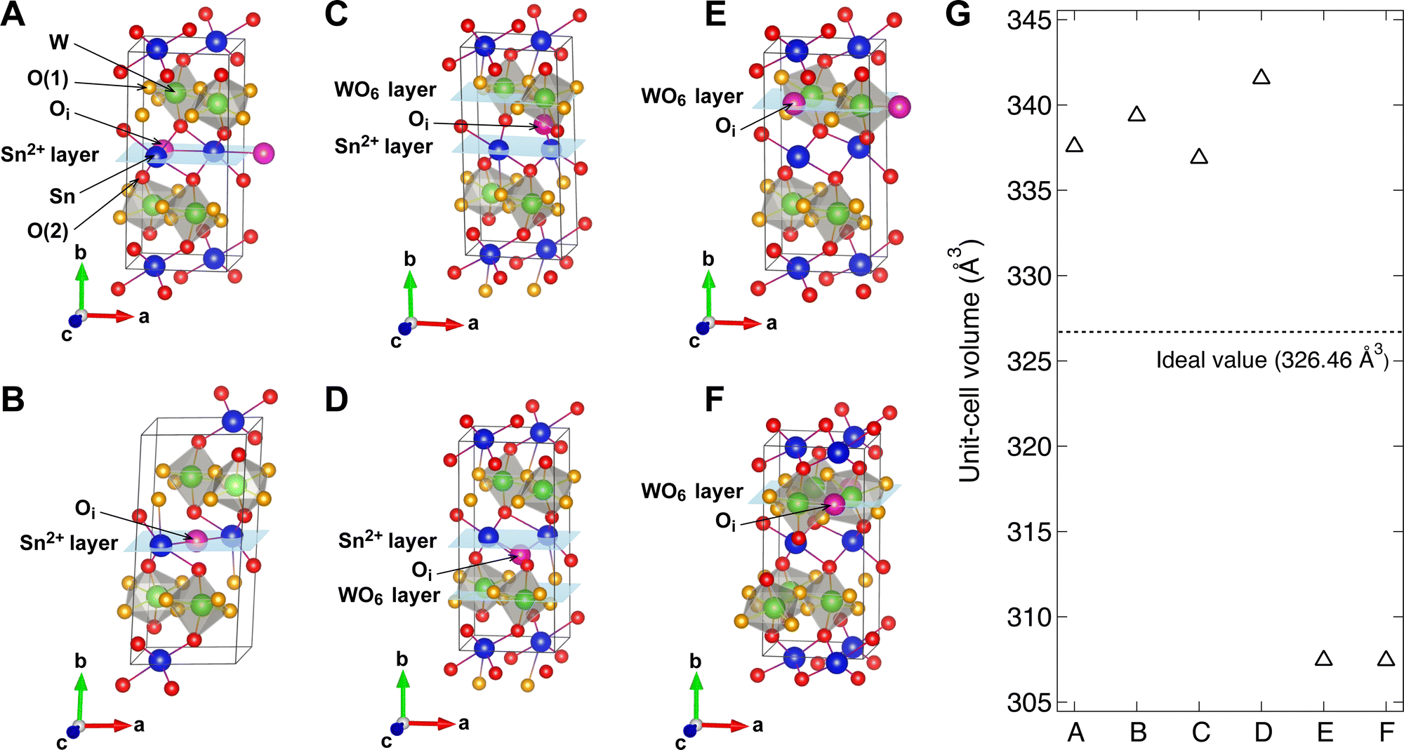 | ||
| Fig. 4 (A–F) Candidate structures of interstitial oxygen in α-SnWO4 samples for DFT calculations. (G) Calculated unit-cell volume of α-SnWO4 with Oi formed at each position. | ||
To obtain further insight into the oxygen defects in the α-SnWO4 samples, EXAFS measurements were performed. Fig. 5A and B show the representative Fourier-transform (FT) magnitudes of the EXAFS data for the Sn K- and W L3-edges, respectively. These spectra exhibit two prominent features at 1.5–1.8 Å and 3.2–3.5 Å, caused by single scattering from the O and Sn/W atoms, respectively. Based on an assumption that the Debye–Waller factor of each atom does not change, the changes in intensity reflect the number of oxygen atoms. The intensity of the FT corresponding to the contributions of the nearest-neighbor (NN) Sn–O scattering peak was nearly unchanged from 0 ppm to 40 (or 50) ppm and clearly increased when the O2 gas concentration was above 50 ppm (see also Fig. S5, ESI†). By contrast, the intensity of the W–O scattering peaks was maintained for all samples.
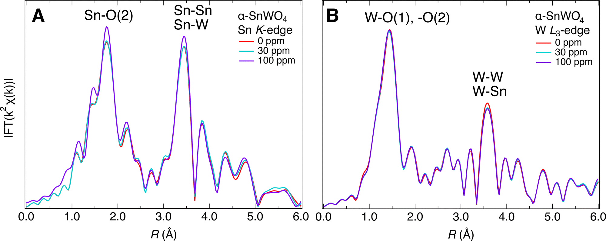 | ||
| Fig. 5 k 2-Weighted Fourier-transformed (A) Sn K-edge and (B) W L3-edge spectra of representative α-SnWO4 samples. R is interatomic distance without correction obtained from photoelectron phase shift. | ||
Quantitatively, the carrier density changes (from 7 × 1016 cm−3 to 8 × 1018 cm−3) in the range 0 to 30 ppm correspond to a change in the concentration of  from 0.87 at% to 0.86 at% at a constant concentration of
  of 3.5 at%.15 However, in actuality, the changes in the concentration of
  should be less than the estimated values because the increment in the O2 gas concentration will affect not only the amount of
  but also that of
  , as mentioned in the introductory section. In this case, negligible changes in the intensities of the Sn–O and W–O scattering peaks would be reasonable. Here, it should be an important fingerprint for the Oi that a clear increment in the intensity was observed only for the Sn–O scattering peaks, which are composed of Sn–O(2) bonds, at higher O2 gas concentrations. If the amount of oxygen at the O(2) site in α-SnWO4 increases, a similar trend is expected for the intensities of the W–O scattering peaks because these peaks contain both W–O(1) and W–O(2) bonds. Therefore, it is possible that the prominent features at ∼1.8 Å in the FT magnitude of the EXAFS data for the Sn K-edge (Fig. 5A) reflect not only Sn–O(2) but also Sn–Oi. The calculated distances for Sn–Oi and W–Oi strongly depend on the position of Oi formation (Fig. S6, ESI†). Among the calculated structures shown in Fig. 4, structures A, B, and D can well explain the experimental findings from the XRD and EXAFS measurements. Of these, the most stable energy was calculated for structure D. However, the energy differences between the structures were within 40 meV per atom; thus, structures A, B, and D might coexist in actual samples.
In general, interstitial oxygen defects in oxides generate hole carriers. However, first-principles calculations suggest that the Oi in SnO does not contribute to hole/electron conductivity because there is no defect transition level in the calculated band gap.36,37 Furthermore, the lone-pair electrons around the NN Sn ions are absorbed by Oi, and consequently, the density of states around the VBM is drastically decreased.36 This phenomenon potentially triggers a decrease in the hole carrier density.
Conclusions
In summary, the dependence of hole carrier density on O2 gas concentration during the annealing of α-SnWO4 was investigated. The objective was to be able to tune these carrier densities via adjustments to the O2 gas concentration. It was observed that the hole carrier density increased by two orders of magnitude and achieved a value close to 1019 cm−3 at an optimum O2 gas concentration. At O2 gas concentrations higher than the optimum, the hole carrier density decreased and became finally saturated at approximately mid-1017 cm−3. Both experimental and theoretical approaches showed that the first increment in the hole carrier density was well explained by the suppression of oxygen vacancy formation, whereas the subsequent decrease in hole carrier density could be due to the formation of interstitial oxygen. This study confirms the necessity of fine-tuning thermodynamic conditions to improve the semiconducting properties of Sn2+-based p-type oxides.Author contributions
M. M., N. K., and K. N. designed the experiments. Y. D. synthesized the materials. M. M., Y. D., N. K., A. S., and Y. A. performed the EXAFS measurements. M. M., N. K., A. S., and T. H. performed the SR-XRD measurements. X. H., Ta. K., and To. K. simulated the structural deformation based on density functional theory calculations.Conflicts of interest
There are no conflicts of interest to declare.Acknowledgements
We thank Dr H. Nitani and Dr H. Sagayama for providing technical support for the beamline experiments. M. M. would like to thank Dr H. Ohta for checking the reproducibility of the thermopower measurements. This work was supported by Grant-in-Aid for Scientific Research (No. 18K04946 and 18K05285) from the Japan Society for the Promotion of Science (JSPS). The work at KEK-PF was performed with the approval of the Program Advisory Committee (Proposals No. 2019G543, 2020G542, and 2021PF-Q009) at the Institute of Materials Structure Science, KEK. We would like to thank Editage (http://www.editage.com) for the English language editing.Notes and references
- J. Shi, J. Zhang, L. Yang, M. Qu, D.-C. Qi and K. H. L. Zhang, Adv. Mater., 2021, 33, 2006230 CrossRef PubMed.
- H. Kawazoe, M. Yasukawa, H. Hyodo, M. Kurita, H. Yanagi and H. Hosono, Nature, 1997, 389, 939 CrossRef.
- Z. Wang, P. K. Nayak, J. A. Coraveo-Francas and H. N. Alshareef, Adv. Mater., 2016, 28, 3831 CrossRef PubMed.
- H. Kawazoe, H. Yanagi, K. Ueda and H. Hosono, MRS Bull., 2000, 25, 28 CrossRef.
- G. Hautier, A. Miglio, G. Ceder, G.-M. Rignanese and H. Gonze, Nat. Commun., 2013, 4, 2292 CrossRef PubMed.
- H. Hosono, Thin Solid Films, 2007, 515, 6000 CrossRef.
- Y. Ogo, H. Hiramatsu, K. Nomura, H. Yanagi, T. Kamiya, M. Hirano and H. Hosono, Appl. Phys. Lett., 2008, 93, 032113 CrossRef.
- T. Li, S. Luo, X. Wang and L. Zhang, Adv. Mater., 2021, 33, 3008574 Search PubMed.
- J. A. Caraveo-Frescas, P. K. Nayak, H. A. Al-Jawhari, D. B. Granato, U. Schwingenschlögl and H. N. Alshareef, ACS Nano, 2013, 7, 5160 CrossRef PubMed.
- M. Minohara, N. Kikuchi, Y. Yoshida, H. Kumigashira and Y. Aiura, J. Mater. Chem. C, 2019, 7, 6332 RSC.
- M. Minohara, A. Samizo, N. Kikuchi, K. K. Bando, Y. Yoshida and Y. Aiura, J. Phys. Chem. C, 2000, 124, 1755 CrossRef.
- A. Bhatia, G. Hautier, T. Nilgianskul, A. Miglio, J. Sun, H. J. Kim, K. H. Kim, S. Chen, G.-M. Rignanese and X. Gonze, Chem. Mater., 2016, 28, 30 CrossRef CAS.
- N. Kikuchi, A. Samizo, S. Ikeda, Y. Aiura, K. Mibu and K. Nishio, Phys. Rev. Mater., 2017, 1, 021601 CrossRef.
- A. Samizo, N. Kikuchi, Y. Aiura, K. Nishio and K. Mibu, Chem. Mater., 2018, 30, 8221 CrossRef CAS.
- M. Minohara, Y. Dobashi, N. Kikuchi, A. Samizo, K. Tsukuda, K. Nishio, K. Mibu, H. Kumigashira, I. Hase, Y. Yoshida and Y. Aiura, Inorg. Chem., 2021, 60, 8035 CrossRef CAS PubMed.
- J. Shi, E. A. Rubinstein, W. Li, J. Zhang, Y. Yang, T.-L. Lee, C. Qin, P. Yan, J. L. MacManus-Driscoll, D. O. Scanlon and K. H. L. Zhang, Adv. Sci., 2022, 9, 2104141 CrossRef CAS PubMed.
- M. Minohara, N. Kikuchi, K. Tsukuda, Y. Dobashi, A. Samizo, K. Nishio, X. He, T. Katase, T. Kamiya and Y. Aiura, Mater. Des., 2022, 216, 110549 CrossRef CAS.
- Y. Hu, X. Yao, D. G. Schlom, S. Datta and K. Cho, Chem. Mater., 2021, 33, 212 CrossRef CAS.
- S. Katayama, Y. Ogawa, H. Hayashi, F. Oba and I. Tanaka, J. Cryst. Growth, 2015, 416, 126 CrossRef CAS.
- S. Katayama, H. Hayashi, Y. Kumagai, F. Oba and I. Tanaka, J. Phys. Chem. C, 2016, 120, 9604 CrossRef CAS.
- H. Ito, T. C. Fujita and M. Kawasaki, APL Mater., 2021, 9, 101116 CrossRef CAS.
- M. Barone, M. Foody, Y. Hu, J. Sun, B. Frye, S. S. Perera, B. Subedi, H. Paik, J. Hollin, M. Jeong, K. Lee, C. H. Winter, N. J. Podraza, K. Cho, A. Hock and D. G. Schlom, J. Phys. Chem. C, 2022, 126, 3764 CrossRef CAS.
- D. Dahliah, G.-M. Rignanese and G. Hautier, J. Mater. Chem. C, 2020, 8, 9352 RSC.
- A. Samizo, M. Minohara, N. Kikuchi, K. K. Bando, Y. Aiura and K. Nishio, J. Phys. Chem. C, 2021, 125, 17117 CrossRef CAS.
- R. Oishi, M. Yonemua, Y. Nishimaki, S. Torii, A. Hoshikawa, T. Ishigaki, T. Morhisima, K. Mori and T. Kamiyama, Nucl. Instrum. Methods Phys. Res., Sect. A, 2009, A600, 94 CrossRef.
- R. Oishi-Tomiyasu, M. Yonemura, T. Morishima, A. Hoshikawa, S. Torii, T. Ishigaki and T. Kamiyama, J. Appl. Crystallogr., 2012, 45, 299 CrossRef CAS.
- K. Momma and F. Izumi, J. Appl. Crystallogr., 2011, 44, 1272 CrossRef CAS.
- M. Nomura, T. Koike, M. Sato, A. Koyama, Y. Inada and K. Asakura, AIP Conf. Proc., 2007, 882, 896 CrossRef CAS.
- B. Ravel and M. Newville, J. Synchrotron Radiat., 2005, 12, 537 CrossRef CAS PubMed.
- G. Kresse and D. Joubert, Phys. Rev. B: Condens. Matter Mater. Phys., 1999, 59, 1758 CrossRef.
- G. Kresse and J. Furthmüller, Phys. Rev. B: Condens. Matter Mater. Phys., 1996, 54, 11169 CrossRef PubMed.
- J. P. Perdew, A. Ruzsinszky, G. I. Csonka, O. A. Vydrov, G. E. Scuseria, L. A. Constantin, X. Zhou and K. Burke, Phys. Rev. Lett., 2008, 100, 136406 CrossRef PubMed.
- W. J. Kim, W. Chang, S. B. Qadri, J. M. Pond, S. W. Kirchoefer, D. B. Chrisey and J. S. Horwitz, Appl. Phys. Lett., 2000, 76, 1185 CrossRef.
- T. Ohnishi, K. Shibuya, T. Yamamoto and M. Lippmaa, J. Appl. Phys., 2008, 103, 103703 CrossRef.
- J. D. Jorgensen, B. Dabrowski, S. Pei, D. R. Richards and D. G. Hinks, Phys. Rev. B: Condens. Matter Mater. Phys., 1989, 40, 2187 CrossRef CAS.
- A. Togo, F. Oba, I. Tanaka and K. Tatsumi, Phys. Rev. B: Condens. Matter Mater. Phys., 2006, 74, 195128 CrossRef.
- J. P. Allen, D. O. Scanlon, L. F. J. Piper and G. W. Watson, J. Mater. Chem. C, 2013, 1, 8194 RSC.
Footnote |
| † Electronic supplementary information (ESI) available: Thermopower versus temperature difference, optical band gap, lattice constants of a, b, and c-axes, and Sn/W ratio of α-SnWO4 samples (S1–S4), plots of intensity in EXAFS spectra (S5), and calculated bond lengths of candidate structures (S6). See DOI: https://doi.org/10.1039/d2ma00815g |
| This journal is © The Royal Society of Chemistry 2022 |