
 Open Access Article
 This Open Access Article is licensed under a Creative Commons Attribution-Non Commercial 3.0 Unported Licence
Effect of substrate nitridation and a buffer layer on the growth of a non-polar a-plane GaN epitaxial layer on an r-plane sapphire substrate by laser molecular beam epitaxy
Prashant
Tyagi†
ab,
Bipul Kumar
Pradhan
ab,
Amit Kumar
Mauraya
ab,
Debashrita
Mahana
ab,
Vishnu
Aggarwal
ab,
Govind
Gupta
ab,
Sunil Singh
Kushvaha
 ab and
Senthil Kumar
Muthusamy
*ab
ab and
Senthil Kumar
Muthusamy
*ab
aCSIR – National Physical Laboratory, Dr K.S. Krishnan Road, New Delhi-110012, India. E-mail: senthilmk@nplindia.org
bAcademy of Scientific and Innovative Research (AcSIR), Ghaziabad-201002, India
First published on 19th September 2022
Abstract
Non-polar a-plane GaN epitaxial layers have been successfully grown on r-plane sapphire substrates by using the laser molecular beam epitaxy (LMBE) technique through the laser ablation of a GaN solid target under radio frequency nitrogen plasma ambient at a low temperature of 600–700 °C. The role of sapphire nitridation and GaN and AlN buffers on the growth and properties of the a-plane GaN layer on r-sapphire has been investigated. Sapphire nitridation is found to produce the growth of a c-axis oriented, high-density GaN nanorod array on r-plane sapphire. However, a direct growth of GaN on r-sapphire without nitridation yields an a-plane GaN layer as confirmed with in situ reflective high energy electron diffraction, X-ray diffraction, and field-emission scanning electron microscopy observations. The introduction of low temperature (LT) GaN or high temperature (HT) AlN buffer on r-sapphire improved the optical quality of the a-plane GaN layers on r-plane sapphire with a strong band-to-band photoluminescence transition and low defect level emission at room temperature. Among the adopted approaches, HT–AlN buffer is found to be effective for improving the morphological, structural and optical properties of a-plane GaN layers grown on r-plane sapphire. A fully coalesced flat surface GaN layer is achieved under two-dimensional growth mode. The results indicate that the optimization of the pre-growth procedure is very critical to achieve a flat surface nonpolar a-plane GaN epitaxial layer on r-plane sapphire in the LMBE process.
Introduction
In the past two decades, researchers around the globe have been investigating the growth of nonpolar and semipolar GaN for high efficiency light emitting diode (LED) and laser diode (LD) applications.1–6 For the growth of GaN on a sapphire substrate, the most suitable orientation is c-plane due to high growth rate and good crystalline quality achieved in this direction. But, GaN layers and heterostructures grown along this polar orientation are subjected to polarization-induced charge which causes a huge electric field in III-nitride heterostructures. On the one hand, this built-in electric field confines two dimensional electron gas (2DEG) at the AlGaN/GaN hetero-interface, which has led to the amazing development of high electron mobility transistor (HEMT) devices.7,8 On the other hand, the electric-field present in GaN based quantum well structures subsequently leads to a quantum confined stark effect (QCSE).9,10 The QCSE hampers the performance of optoelectronic devices such as LEDs and LDs and causes a spatial separation of electrons and holes reducing their recombination efficiency, which lowers the quantum efficiency of these devices.9 This problem could be evaded by changing the growth orientation to non-polar a-plane [11−20] or m-plane [1−100]; in these orientations, the c-axis is parallel to the substrate and hence, there would be no polarization induced electric field in the vertical direction.11,12 This reduction in the electric field effectively eliminates the QCSE at the heterostructure interface, which enhances the efficiency of fabricated devices.13,14 In this quest, the heteroepitaxy of non-polar GaN on foreign substrates like m-plane SiC, γ-LiAlO2, r-plane sapphire, etc., has been investigated. Here, the growth of a-plane GaN on an r-plane sapphire substrate is preferred due to scientific and commercial feasibility. However, in this orientation, GaN growth suffers high stacking faults and dislocation densities and it is difficult to prepare good quality non-polar GaN with good surface morphology on r-plane sapphire substrates.15,16There are reports which suggest that the growth of non-polar GaN could be realized on r-plane sapphire by metal organic chemical vapour deposition (MOCVD) and molecular beam epitaxy (MBE), but there are still some limitations that need to be overcome.17–20 The major problem faced with non-polar GaN growth is associated with the thick interfacial layer that exists between a-plane GaN and r-plane sapphire due to high temperature growth. In order to overcome these limitations, thicker GaN epilayers are grown up to a few tens of microns.21 Thus, there is a need to develop low temperature growth processes for a-plane GaN epitaxial layers which could eliminate the formation of the thick interfacial layer and also reduce the thermal mismatch (i.e. 27%).22 Laser molecular beam epitaxy (LMBE) is demonstrated as an effective technique for the growth of GaN layers at relatively low temperatures on a variety of substrates.23–25 To date, there are only very few reports available on the growth of non-polar GaN on r-plane sapphire using the LMBE technique.26–28 Six et al. reported non-polar AlN growth on r-plane sapphire substrates by pulsed laser deposition (PLD), but the grown films were polycrystalline with both a- and c-axis orientations.26 Also, the optimized growth conditions for epitaxial films have not been defined properly. Yang et al. have reported the growth of a-plane GaN on r-plane sapphire by an ultra-high vacuum (UHV) PLD process with island morphology at an optimised growth temperature of 850 °C with substrate nitridation.27 Later, the same group employed PLD grown smooth surface a-plane GaN epitaxial films on r-plane sapphire substrates as a template for MOCVD GaN growth and obtained a better quality a-plane GaN film with a thickness of 2.9 μm by the combined growth process.28 Still, the growth of nonpolar a-plane GaN epilayers by the LMBE technique is at its beginning stage and further research work is necessary to understand and develop the LMBE process for high quality nonpolar a-plane GaN growth for device applications. In this report, we study the effect of substrate nitridation and different buffer layers on the growth of a-plane GaN epitaxial layers on an r-plane sapphire substrate in the LMBE process and demonstrate the flat surface growth of a thin (100–200 nm) GaN layer on r-sapphire with good optical emission properties using high temperature AlN buffer.
Experimental
Non-polar a-plane GaN epitaxial growth was performed on r-plane sapphire in an LMBE system with different pre-growth procedures, such as sapphire nitridation and GaN/AlN buffer growth. The r-plane sapphire substrate does not have any miscut orientation. Initially, sapphire substrates were cleaned with standard organic solutions and de-ionised water before loading into the load-lock chamber of the LMBE system, where they were degased at 250 °C for three hours under a high vacuum in the order of 5 × 10⁻⁷ Torr. Subsequently, the substrates were transferred into the growth chamber where they were thermally cleaned at 850 °C for twenty minutes under UHV conditions. GaN layers were grown by the laser ablation of a hydride vapour phase epitaxy grown polycrystalline GaN target (6N pure) in r.f. plasma ambient. A KrF excimer laser having 248 nm wavelength and 25 ns pulse width was used to ablate the target material. The laser energy density and repetition rate were kept as 3–4 J cm−2 and 20 Hz, respectively. In order to maintain the stoichiometry of GaN, additional nitrogen radicals were supplied by an r.f. nitrogen plasma cell. The plasma power and nitrogen partial pressure were kept constant at 250 W and 2.4 × 10⁻⁵ Torr, respectively, during GaN and AlN growth. The sapphire substrate was kept at ∼6 cm above the target and rotated at a speed of 2 rpm during the entire growth process for spatial uniformity. The growth duration of GaN was kept constant as 3 h. The growth rate of nonpolar GaN on r-sapphire was estimated by measuring the thickness of the grown layers using a Stylus profilometer. The growth rate of a-plane GaN is estimated to be 70 nm h−1 at 500 °C, which is reduced to 35 nm h−1 at 700 °C. The decrease in growth rate with increasing temperature could be attributed to the increased desorption of adatoms from the growth surface at higher temperatures.29,30GaN samples were prepared with different combinations of growth steps in order to determine an optimal growth sequence of non-polar GaN on r-plane sapphire in the LMBE process. The growth steps involved are sapphire-nitridation or no-nitridation, low temperature (LT) GaN buffer or high temperature (HT) AlN buffer and GaN epilayer growth. The sapphire nitridation was carried out at 700 °C for 35 min under r.f. nitrogen plasma with a nitrogen partial pressure of 6.7 × 10⁻⁵ Torr and a r.f. plasma power of 400 W. GaN was grown on both bare and pre-nitridated r-sapphire substrates. In further growth runs, GaN epilayers were grown on bare r-plane sapphire using LT grown GaN buffer and HT grown AlN buffer. The GaN buffer layer was grown at 500 °C for 20 min while the AlN buffer layer was grown at 800 °C for 30 min. For the growth of AlN buffer, a sintered AlN solid target of 3N purity was ablated using the laser energy density of ∼6 J cm−2 and the repetition rate of 20 Hz under the continuous supply of r.f. nitrogen plasma. The main GaN layers were grown at an optimized temperature of 700 °C in all cases except for GaN buffer. For the GaN buffer sample, the optimized growth temperature of the main GaN was 600 °C.
The entire LMBE growth process of GaN was monitored with an in situ reflection high-energy electron diffraction (RHEED) observation. The surface morphology of grown GaN was studied using field-emission scanning electron microscopy (FE-SEM) (FIB, ZEISS, Germany). The crystalline properties of GaN epitaxial layers have been characterized by high resolution X-ray diffraction (HRXRD) using a PANalytical HR-XRD system with a Cu Kα1 source. Room temperature photoluminescence (RT-PL) characterization was employed in order to evaluate the optical properties of GaN using a 325 nm He–Cd laser as the excitation source.
Results and discussion
It is well known that, in GaN growth on c-plane sapphire substrates, the nitridation of sapphire leads to the formation of a few monolayers of AlN and/or AlOxNy on the surface, which can mediate GaN growth to obtain a low defect density in the layer.31–34 After the nitridation process of r-plane sapphire, we noticed the attenuation of the RHEED intensity of the sapphire substrate with elongated streaky features similar to the nitridation of c-plane sapphire at high temperature, which could indicate the modification of the sapphire surface likely due to the formation of AlN and/or AlOxNy.33,34 Here, the effect of r-plane sapphire nitridation on non-polar GaN growth by the LMBE technique has been examined. Fig. 1 presents the FESEM surface morphology (top view and 45° tilt-view) of the LMBE GaN layer grown on pre-nitridated r-sapphire at 700 °C. In the FESEM image, well-ordered, high-density, and mutually inclined-nanorods are obtained. The hexagonal shape of the nanorods suggests the wurtzite structure and c-axis orientation. The angle of the nanorods with the substrate normal is measured to be around 60°. The diameter of the grown nanorods is in the range of 45–65 nm and the length is in the range of 200–240 nm. The nanorod density was estimated to be around 1.8 × 1010 cm−2. In contrast, instead of nanorods, Yang et al. have obtained island growth of the a-plane GaN epitaxial layer on the high temperature nitridated r-plane sapphire substrate in the growth temperature range of 450–880 °C using the PLD process.27 However, Aschenbrenner et al. and Adikimenakis et al. have reported similar observation of the growth of GaN nanorods on pre-nitridated r-sapphire using MOVPE and MBE techniques, respectively.35,36 During the nitridation of the sapphire substrate, uncoalesced AlN islands form over the sapphire surface. These pyramid-shaped island facets act as nucleation sites for the growth of inclined polar GaN nanorods as schematically illustrated in Fig. 2.35 The growth of GaN nanorods is a mostly diffusion enhanced process as explained in various reports.37–39 The RT-PL spectrum of the GaN nanorods is presented in Fig. 1(d) where a strong near band emission (NBE) has been obtained at 3.41 eV along with a low intensity broad peak of the yellow luminescence (YL) band. The full width at half maximum (FWHM) value of the NBE peak is estimated to be about 146 meV. The intense and narrow NBE emission indicates that the RT-PL spectrum is primarily dominated by a c-axis oriented high quality nanorod array rather than by non-polar GaN.36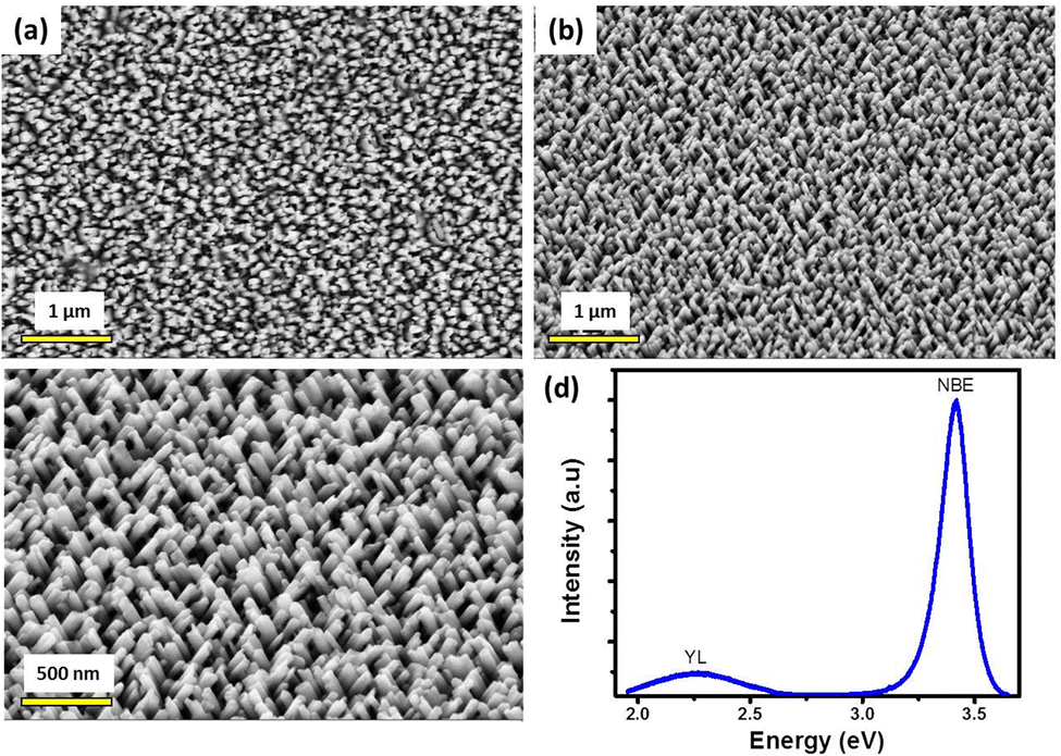 | ||
| Fig. 1 (a) Top-view and (b) and (c) 45° tilt-view FESEM images of GaN grown on a pre-nitrided r-plane sapphire substrate. (d) Room temperature photoluminescence spectrum of the respective sample. | ||
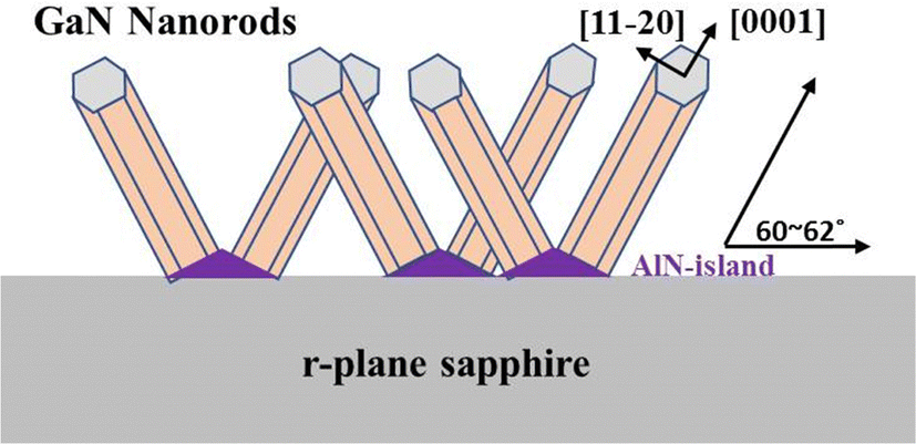 | ||
| Fig. 2 Schematic of GaN growth on pre-nitrided r-sapphire including the crystallographic direction of the GaN nanorods.29 | ||
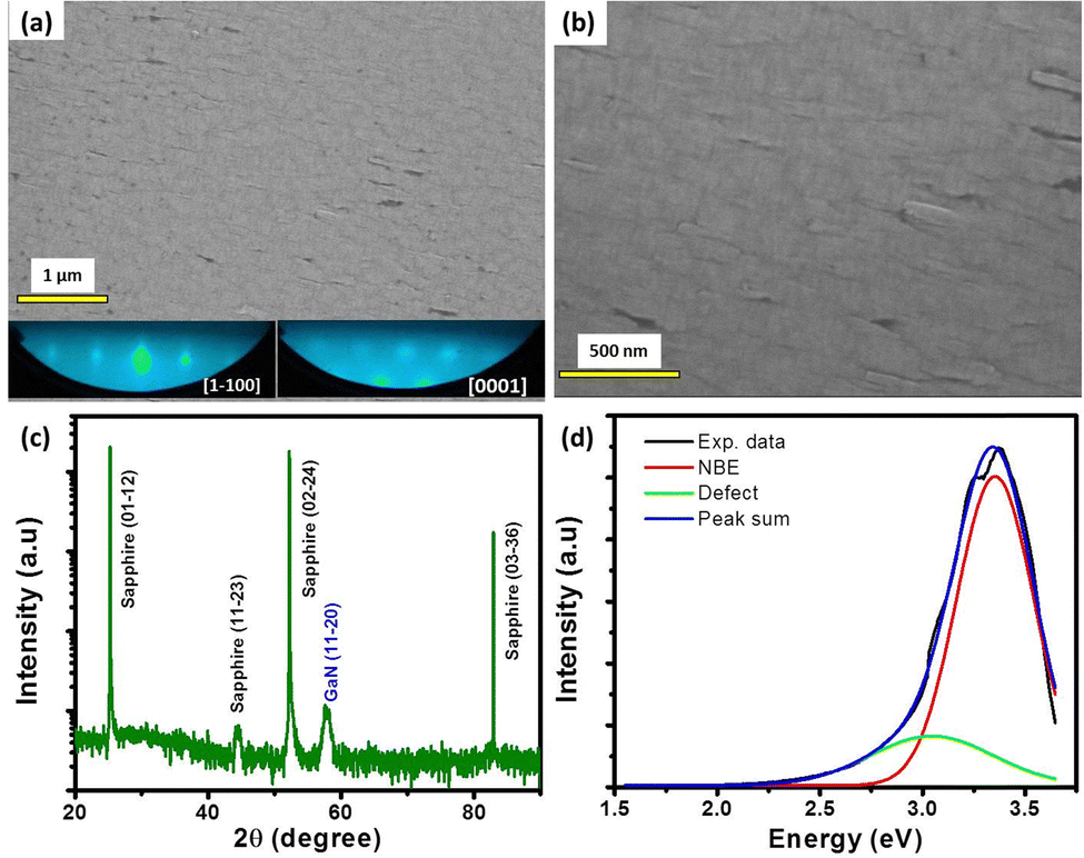
Fig. 3 presents the in situ RHEED pattern and FESEM surface morphology (top-view) of LMBE GaN layers directly grown on r-sapphire without substrate nitridation. The image shows a flat surface morphology consisting of undulation features. This surface feature is a signature of a-plane GaN growth on r-plane sapphire as widely reported and is referred to as ‘striation’ which occurs due to the different growth rates of wurtzite GaN along different directions.39–42 The striations are formed along the c-direction as a result of the relatively higher growth rate in this direction. The RHEED pattern recorded along azimuths of [1−100] and [0001] at the end of GaN growth confirms the epitaxial growth of a-plane GaN on r-plane sapphire. Here, the steak-like pattern along [1−100] and spotty pattern along [0001] azimuths could indicate the anisotropic nature of GaN growth on r-plane sapphire. In the literature, using a similar process, a surface morphology of island growth has been reported for the a-plane GaN grown at 850 °C on pre-nitridated r-plane sapphire.27Fig. 3(c) gives the XRD ω–2θ scan of a-plane GaN grown on a bare r-sapphire substrate. The spectrum shows the (11−20) peak of GaN along with r-plane sapphire peaks complimenting the RHEED observation of a-plane GaN growth on r-plane sapphire. The FWHM of the GaN (11−20) peak is obtained as 0.95°. A small inclusion of sapphire (11−23) grains is noticed in the r-plane substrate with a low intensity peak. The RT-PL spectrum of the a-plane GaN layer is given in Fig. 3(d). The spectrum exhibited a broad UV emission peak in the energy range of 2.5 to 3.5 eV, which reveals a poor optical quality of the grown GaN film. The PL peak was de-convoluted by fitting with two Gaussians. The near-band-edge (NBE) emission is seen at 3.39 eV with a FWHM value of 370 meV. A broad defect emission band is observed to be positioned at around 3.12 eV.
 | ||
| Fig. 3 (a) and (b) FESEM images of the a-plane GaN layer directly grown on an r-plane sapphire substrate at different magnifications. The inset of (b) shows the in situ RHEED observation along the [1−100] and [0001] azimuths of GaN. (c) ω–2θ scan X-ray diffraction spectrum and (d) room-temperature photoluminescence spectrum of the respective sample. | ||
In the heteroepitaxial growth of GaN on sapphire, it is also well known that a buffer, i.e., a thin layer of GaN or AlN before the main epitaxial layer growth, can significantly improve the crystalline and optical quality of the GaN layers as it helps to reduce the severity of lattice mismatch between GaN and sapphire. The FESEM and in situ RHEED images of the GaN layer grown on bare r-plane sapphire using an LT–GaN buffer are shown in Fig. 4(a). The RHEED pattern taken along the [1−100] and [0001] azimuths of GaN revealed the epitaxial growth of the non-polar a-plane GaN layer. The FESEM morphology shows a nearly coalesced surface with strip patterns and surface pits in some places. The characteristic striation features of a-plane GaN growth could also be easily noticed. The pit facets often provide nucleation sites for the growth of c-plane GaN nanorods.43
 | ||
| Fig. 4 (a) and (b) FESEM images of the a-plane GaN layer grown on an r-plane sapphire substrate using LT-GaN buffer. The inset of (a) shows the in situ RHEED observation along the [1−100] and [0001] azimuths of the GaN epilayer. (c) ω–2θ scan X-ray diffraction and (d) room-temperature photoluminescence spectra of the respective sample. | ||
The XRD ω–2θ scan of the GaN layer grown on r-sapphire with LT-GaN is given in Fig. 4(c). The spectrum shows a diffraction peak corresponding to only the GaN (11−20) plane that agrees well with RHEED observation. The structural quality of the a-plane GaN layer has been analysed by measuring the FWHM of the GaN (11−20) peak as 1.02°. The RT-PL data, plotted in Fig. 4(d), show a relatively narrow emission spectrum as compared to the a-plane GaN layer directly grown on r-sapphire without any buffer layer. The PL data were analysed using peak fitting with a Gaussian function. The NBE peak is positioned at 3.37 eV and has an FWHM value of 368 meV. The low intensity, broad defect peak is found to be centred at 3.07 eV with an FWHM value of 586 meV. Here, the FWHM of NBE is comparable to the a-plane GaN layer directly grown on r-sapphire, whereas the defect peak FWHM is significantly reduced by the inclusion of LT-GaN buffer in the growth sequence. The further improvement of a-plane GaN growth and its properties was attempted using the HT–AlN buffer layer.
In order to study the effect of HT–AlN buffer, the growth of GaN was carried out on a bare r-plane sapphire using HT–AlN buffer grown at 800 °C. The in situ RHEED and FESEM images are presented in Fig. 5(a) and (b). The surface morphology consists of a smooth GaN layer growth with minimal striation features without any secondary nucleation, which indicates a well-coalesced GaN growth. The RHEED observation confirmed the growth of non-polar a-plane GaN while the bright streak-like pattern along both [1−100] and [0001] azimuths imply an isotropic growth under the two-dimensional mode, which could not be achieved in the previous cases. Fig. 5(c) presents the XRD ω–2θ spectrum of a-plane GaN layers grown on r-sapphire with the HT–AlN buffer layer. It is noted that the XRD peak related to AlN buffer was not observed in the XRD spectrum. The amount of AlN could be probably less for the detection in XRD but the growth of AlN buffer was confirmed with the observation of the weak appearance of the AlN related in situ RHEED pattern at the end of buffer growth, as shown in the inset of Fig. 5(a). The spectrum showed a single diffraction peak corresponding to the GaN (11−20) plane complementing the RHEED observation. The GaN (11−20) peak FWHM value of 0.87° is achieved for the GaN layer grown with HT–AlN buffer, which is lower than the layers grown with and without LT–GaN buffer. This implies that HT–AlN buffer more effectively improves the crystalline quality of the a-plane GaN layer on r-sapphire by the LMBE technique. The RT-PL spectrum of a-plane GaN layers grown on r-sapphire with HT–AlN buffer is given in Fig. 5(d). Here, a strong NBE emission is seen with a shoulder emission peak in the lower energy side. In addition, a broad low intensity peak in the YL region is also detected. Among all a-plane GaN layers grown, better optical properties with strong and sharp NBE emission and less pronounced defect level are obtained for the GaN grown on HT–AlN buffer. The respective PL emission spectrum fitted with Gaussians is presented in Fig. 5(d). The NBE peak is positioned at 3.39 eV and possesses an FWHM value of 242 meV. On the other hand, the defect peak centred at 3.12 eV has an FWHM value of 538 meV. The NBE peak intensity is much stronger than the intensity of defect related emission peaks. From the said observations, we could conclude that HT–AlN buffer improves the optical quality of non-polar GaN as compared to the layers grown using LT–GaN buffer. The YL peak is situated at 2.35 eV, which arises due to the presence of VIII vacancies or increased edge dislocation density.44,45 The XRD and PL data of the a-plane GaN layer grown without buffer and with LT–GaN and HT–AlN buffer are listed in Table 1. In comparison, the a-plane GaN layer grown using HT–AlN buffer has better structural and optical emission properties and a flat surface morphology. The results prove that the LMBE technique can be employed for the development of non-polar III-Nitrides and device quality epilayers can be achieved by further fine-tuning of the growth process.
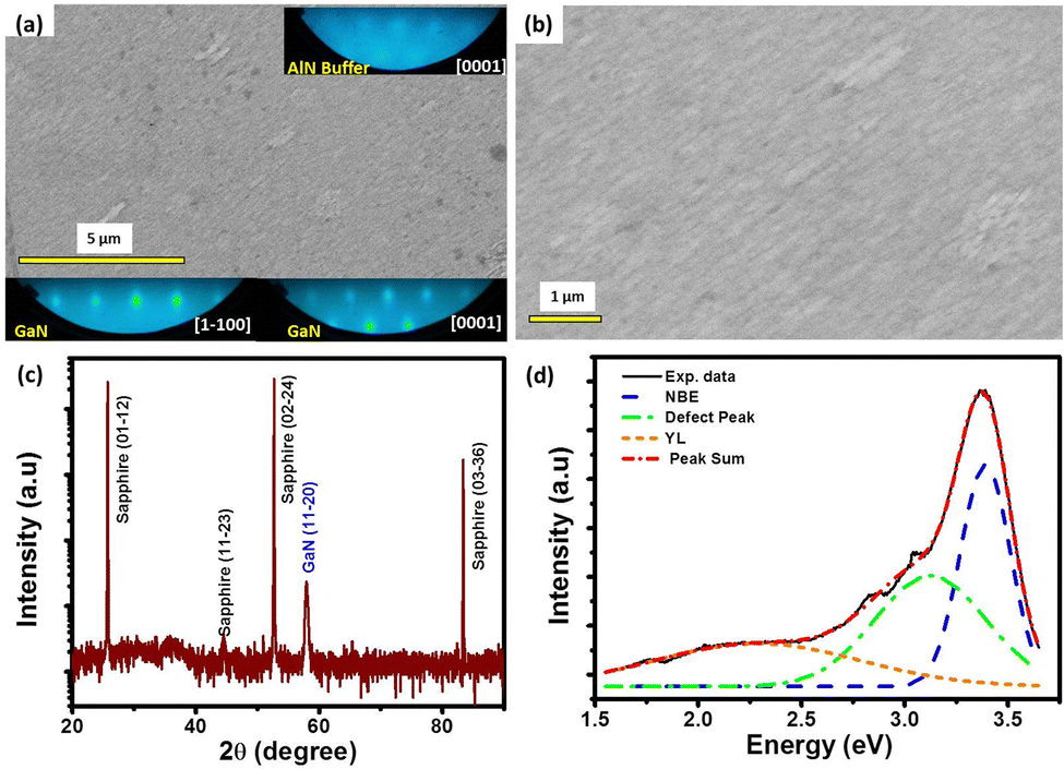 | ||
| Fig. 5 (a) and (b) FESEM images of the a-plane GaN layer grown on an r-plane sapphire substrate using HT-AlN buffer. The insets of (a) show the in-situ RHEED patterns recorded along the [1−100] and/or [0001] azimuths at the end of AlN buffer and GaN epilayer growth. (c) ω–2θ scan X-ray diffraction and (d) room-temperature photoluminescence spectra of the respective sample. | ||
| Buffer | XRD 2θ peak | PL NBE Peak | PL Defect Peak | ||
|---|---|---|---|---|---|
| FWHM (°) | Position (eV) | FWHM (meV) | Position (eV) | FWHM (meV) | |
| No buffer | 0.95 | 3.39 | 370 | 3.12 | 657 |
| LT–GaN | 1.02 | 3.37 | 368 | 3.07 | 586 |
| HT–AlN | 0.87 | 3.39 | 242 | 3.12 | 538 |
| 2.29 | 995 | ||||
Conclusions
Successful growth of nonpolar a-plane GaN epitaxial layers has been realized on an r-plane sapphire substrate by the LMBE technique. The effect of different pre-growth procedures such as substrate nitridation, LT–GaN buffer and HT–AlN buffer has been studied on the growth and properties of nonpolar GaN layers. It is found that sapphire nitridation leads to the formation of aligned GaN nanorods on r-plane sapphire and is not favourable to obtain a-plane GaN epitaxial layers. In contrast, direct GaN growth on r-sapphire promotes an epitaxial nonpolar a-plane layer having a broad PL luminescence emission composed of band-edge emission and a defect level. In the case of buffer growth, GaN layers grown using HT–AlN buffer on r-sapphire resulted in a flat and fully coalesced layer with better structural and optical properties as compared to that grown with LT–GaN buffer. The results indicate that the pre-growth procedure is very critical to optimize the growth process for a high quality nonpolar a-plane GaN epitaxial layer on r-plane sapphire using the LMBE technique. The results demonstrate that the growth of flat surface nonpolar a-plane GaN is achievable with the LMBE technique; however, the growth sequence and associated experimental parameters should be studied comprehensively to achieve device quality layers.Author contributions
Prashant Tyagi: methodology, investigation, formal analysis, visualization, writing – original draft. Bipul Kumar Pradhan: investigation, formal analysis. Amit Kumar Mauraya: investigation. Debashrita Mahana: investigation. Vishnu Aggarwal: formal analysis. Govind Gupta: resources. Sunil Singh Kushvaha: investigation, formal analysis, visualization. M. Senthil Kumar: conceptualization, methodology, investigation, supervision, writing – review & editing.Conflicts of interest
We do not have any conflicts of interest to declare.Acknowledgements
The authors thank Dr B.S. Yadav and Dr S. Ojha for their help in sample characterizations. P. Tyagi, D. Mahana and V. Aggarwal gratefully acknowledge Council for Scientific and Industrial Research (CSIR), India. B. K. Pradhan and A. K. Mauraya would like to thank the University Grant Commission (UGC) for their research fellowships.References
- A. Chakraborty, B. A. Haskell, S. Keller, J. S. Speck, S. P. Denbaars, S. Nakamura and U. K. Mishra, Jpn. J. Appl. Phys., 2005, 44, L173 CrossRef CAS.
- K. Iso, H. Yamada, H. Hirasawa, N. Fellows, M. Saito, K. Fujito, S. P. DenBaars, J. S. Speck and S. Nakamura, Jpn. J. Appl. Phys., 2007, 46, L960 CrossRef CAS.
- D. F. Feezell, M. C. Schmidt, S. P. DenBaars and S. Nakamura, MRS Bull., 2009, 34, 318 CrossRef CAS.
- T. Detchprohm, M. Zhu, Y. Li, Y. Xia, C. Wetzel, E. A. Preble, L. Liu, T. Paskova and D. Hanser, Appl. Phys. Lett., 2008, 92, 241109 CrossRef.
- M. C. Schmidt, K.-C. Kim, R. M. Farrell, D. A. Cohen, M. Saito, K. Fujito, J. S. Speck, S. P. DenBaars and S. Nakamura, Jpn. J. Appl. Phys., 2007, 46, L190 CrossRef CAS.
- D. F. Feezell, M. C. Schmidt, R. M. Farrell, K.-C. Kim, M. Saito, K. Fujito, D. A. Cohen, J. S. Speck, S. P. DenBaars and S. Nakamura, Jpn. J. Appl. Phys., 2007, 46, L284 CrossRef CAS.
- L. Hsu and W. Walukiewicz, J. Appl. Phys., 2001, 89, 1783 CrossRef CAS.
- J. P. Ibbetson, P. T. Fini, K. D. Ness, S. P. DenBaars, J. S. Speck and U. K. Mishra, Appl. Phys. Lett., 2000, 77, 250 CrossRef CAS.
- M.-H. Kim, M. F. Schubert, Q. Dai, J. K. Kim, E. F. Schuberta, J. Piprek and Y. Park, Appl. Phys. Lett., 2007, 91, 183507 CrossRef.
- Y. C. Shen, G. O. Mueller, S. Watanabe, N. F. Gardner, A. Munkholm and M. R. Krames, Appl. Phys. Lett., 2007, 91, 141101 CrossRef.
- J. S. Speck and S. F. Chichibu, MRS Bull., 2009, 34, 304 CrossRef CAS.
- S.-M. Hwang, Y. G. Seo, K. H. Baik, I.-S. Cho, J. H. Baek, S. Jung, T. G. Kim and M. Cho, Appl. Phys. Lett., 2009, 95, 071101 CrossRef.
- S. Nakagawa, H. Tsujimura, K. Okamoto, M. Kubota and H. Ohta, Appl. Phys. Lett., 2007, 91, 171110 CrossRef.
- B. A. Haskell, S. Nakamura, S. P. DenBaars and J. S. Speck, Phys. Status Solidi B, 2007, 244, 2847 CrossRef CAS.
- Q. Sun, C. D. Yerino, T. S. Ko, Y. S. Cho, I.-H. Lee, J. Han and M. E. Coltrin, J. Appl. Phys., 2008, 104, 093523 CrossRef.
- C. F. Johnston, M. J. Kappers, M. A. Moram, J. L. Hollander and C. J. Humphreys, J. Cryst. Growth, 2009, 311, 3295 CrossRef CAS.
- X. Ni, Y. Fu, Y. T. Moon, N. Biyikli and H. Morkoç, J. Cryst. Growth, 2006, 290, 166 CrossRef CAS.
- C. Chen, J. Zhang and J. Yang, et al. , Jpn. J. Appl. Phys., 2003, 42, L818 CrossRef CAS.
- M. K. Rajpalke, T. N. Bhat, B. Roul, M. Kumar, P. Misra, L. M. Kukreja, N. Sinha and S. B. Krupanidhi, J. Cryst. Growth, 2011, 314, 5–8 CrossRef CAS.
- H. Lu, W. J. Schaff and L. F. Eastman, Appl. Phys. Lett., 2003, 83, 1136 CrossRef CAS.
- T. S. Ko, T. C. Wang, R. C. Gao, H. G. Chen, G. S. Huang, T. C. Lu, H. C. Kuo and S. C. Wang, J. Cryst. Growth, 2007, 300, 308 CrossRef CAS.
- L. Zhou, R. Chandrasekaran, T. D. Moustakas and D. J. Smith, J. Cryst. Growth, 2008, 310, 2981 CrossRef CAS.
- P. Tyagi, Ch Ramesh, B. S. Yadav, S. S. Kushvaha and M. S. Kumar, CrystEngComm, 2019, 21, 5448 RSC.
- Y. Kawaguchi, J. Ohta, A. Kobayashi and H. Fujioka, Appl. Phys. Lett., 2005, 87, 221907 CrossRef.
- M. S. Kumar, S. S. Kushvaha and K. K. Maurya, Sci. Adv. Mater., 2014, 6, 1215 CrossRef CAS.
- S. Six, J. W. Gerlach and B. Rauschenbach, Surf. Coat. Technol., 2001, 397, 142 Search PubMed.
- W. Yang, W. Wang, H. Wang, Y. Zhu and G. Li, Mater. Sci. Semicond. Process., 2016, 43, 82 CrossRef CAS.
- W. Yang, Z. Zhang, W. Wang, Y. Zheng, H. Wang and G. Li, Jpn. J. Appl. Phys., 2018, 57, 051001 CrossRef.
- R. D. Vispute, V. Talyansky, R. P. Sharma, S. Choopun, M. Downes, T. Venkatesan, K. A. Jones, A. A. Iliadis, M. A. Khan and J. W. Yang, Appl. Phys. Lett., 1997, 71, 102 CrossRef CAS.
- S. S. Kushvaha, M. Senthil Kumar, K. K. Maurya, M. K. Dalai and N. D. Sharma, AIP Adv., 2013, 33, 092109 CrossRef.
- K. Uchida, A. Watanabe, F. Yano, M. Kouguchi, T. Tanaka and S. Minagawa, J. Appl. Phys., 1996, 79, 3487 CrossRef CAS.
- C. Heinlein, J. K. Grepstad, S. Einfeldt, D. Hommel, T. Berge and A. P. Grande, J. Appl. Phys., 1998, 83, 6023–6027 CrossRef CAS.
- C. Heinlein, J. Grepstad, T. Berge and H. Riechert, Appl. Phys. Lett., 1997, 71, 341–343 CrossRef CAS.
- P. Tyagi, Ch Ramesh, S. S. Kushvaha, M. Mishra, G. Gupta, B. S. Yadav and M. Senthil Kumar, J. Alloys Compd., 2018, 739, 122–128 CrossRef CAS.
- T. Aschenbrenner, C. Kruse, G. Kunert, S. Figge, K. Sebald, J. Kalden, T. Voss, J. Gutowski and D. Hommel, Nanotechnology, 2009, 20, 075604 CrossRef CAS PubMed.
- A. Adikimenakis, A. Lotsari, G. P. Dimitrakopulos, T. Kehagias, K. E. Aretouli, K. Tsagaraki, M. Androulidaki, P. Komninou and A. Georgakilas, J. Appl. Phys., 2015, 117, 244302 CrossRef.
- V. Consonni, V. G. Dubrovskii, A. Trampert, L. Geelhaar and H. Riechert, Phys. Rev. B: Condens. Matter Mater. Phys., 2012, 85, 155313 CrossRef.
- V. Consonni, M. Hanke, M. Knelangen, L. Geelhaar, A. Trampert and H. Riechert, Phys. Rev. B: Condens. Matter Mater. Phys., 2011, 83, 035310 CrossRef.
- X. Ni, U. Ozgur, Y. Fu, N. Biyikli, J. Xie, A. A. Baski and H. Morkoc, Appl. Phys. Lett., 2006, 89, 262105 CrossRef.
- A. Govorkov, A. Donskov, L. Diakonov, Y. Kozlova, S. Malahov, A. Markov, M. Mezhennyi, V. Pavlov, A. Polykov and T. Yugova, Phys. B, 2009, 404, 4919 CrossRef CAS.
- S. Tripathy and R. K. Soni, J. Appl. Phys., 1999, 85, 8386 CrossRef CAS.
- M. D. Craven, S. H. Lim, F. Wu, J. S. Speck and S. P. DenBaars, Appl. Phys. Lett., 2002, 81, 469 CrossRef CAS.
- Q. Sun and J. Han, Springer series and material science, 2012, pp. 1–27, vol. 156 Search PubMed.
- D. Basak, M. Lachab, T. Nakanishi and S. Sakai, Appl. Phys. Lett., 1999, 75, 3710–3712 CrossRef CAS.
- D. G. Zhao, D. S. Jiang, H. Yang, J. J. Zhu, Z. S. Liu, S. M. Zhang, J. W. Liang, X. Li, X. Y. Li and H. M. Gong, Appl. Phys. Lett., 2006, 88, 241917 CrossRef.
Footnote |
| † Present address: Skyline Semiconductor, SAS Nagar, Mohali-160059, India. |
| This journal is © The Royal Society of Chemistry 2022 |