
 Open Access Article
 This Open Access Article is licensed under a Creative Commons Attribution-Non Commercial 3.0 Unported Licence
Enhanced triboelectric performance of graphene oxide-conducting polymer hybrid modified polydimethylsiloxane composites†
E. J.
Jelmy
a,
Divya
Jose
ab,
K. V.
Vijoy
c,
K. J.
Saji
cd and
Honey
John
 *ade
*ade
aDepartment of Polymer Science and Rubber Technology, Cochin University of Science and Technology, Cochin-22, Kerala, India. E-mail: honey@cusat.ac.in
bDepartment of Chemistry, Bharata Mata College, Thrikkakara Cochin-21, Kerala, India
cInternational School of Photonics, Cochin University of Science and Technology, Cochin-22, Kerala, India
dInter University Centre for Nanomaterials and Devices, Cochin University of Science and Technology, Cochin-22, Kerala, India
eCentre of Excellence in Advanced Materials, Cochin University of Science and Technology, Cochin-22, Kerala, India
First published on 19th July 2022
Abstract
Energy harvesting nanogenerators have received significant attention as they utilize unused mechanical energy from the ambient environment. Nanogenerators based on the triboelectric effect display superior output performance to other types of nanogenerators. In this study, a triboelectric nanogenerator (TENG) based on polydimethylsiloxane (PDMS) is developed by incorporating binary hybrids of graphene oxide (GO) and conducting polymers (CPs) such as polyaniline (PANI) or polypyrrole (PPy) into the bulk of PDMS by an ultrasonication assisted dispersion technique at room temperature. Of various PDMS composites, higher TENG performances were observed for 1![[thin space (1/6-em)]](https://www.rsc.org/images/entities/char_2009.gif) :4 GO:PANI (23.88 V and 0.515 mA m−2) and 1:4 GO:PPy (27 V and 0.501 mA m−2) filler added systems. The primary reason for the enhancement in the TENG performance of the PDMS composite is the improvement in the dielectric properties. The GO and CP ratios in the binary hybrids change the dielectric properties of the PDMS composite by various phenomena such as dielectric polarization including electronic, vibrational, orientation, ionic, and interfacial polarization. Secondly, the electron donating–accepting process between PDMS and the GO/CP filler enhances the surface charge density of the PDMS composite and overall TENG performance. The presence of electron trapping GO in the filler can also improve the charge density of the composite material. Therefore, the superior performances of GO/CP-PDMS composites to neat PDMS can be attributed to the intensified negative charges on PDMS from the functional groups of GO, PANI, or PPy chains and the enhanced dielectric properties. Also, it was observed that the PANI nanofiber intercalated GO morphology of the GO/PANI hybrid in the PDMS composite resulted in better current generation when compared to the PPy nanosphere intercalated GO incorporated PDMS system. The energy harvesting studies using the PDMS composites were demonstrated using various body movements such as single finger tapping and foot stamping. A current of 40 nA and a voltage of 208 V were generated by finger tapping, whereas a short circuit current of 2 μA and a voltage of 27 V were generated by foot stamping or walking. These studies hint at the utility of the proposed material for mechanical energy harvesting using simple body movements.
:4 GO:PANI (23.88 V and 0.515 mA m−2) and 1:4 GO:PPy (27 V and 0.501 mA m−2) filler added systems. The primary reason for the enhancement in the TENG performance of the PDMS composite is the improvement in the dielectric properties. The GO and CP ratios in the binary hybrids change the dielectric properties of the PDMS composite by various phenomena such as dielectric polarization including electronic, vibrational, orientation, ionic, and interfacial polarization. Secondly, the electron donating–accepting process between PDMS and the GO/CP filler enhances the surface charge density of the PDMS composite and overall TENG performance. The presence of electron trapping GO in the filler can also improve the charge density of the composite material. Therefore, the superior performances of GO/CP-PDMS composites to neat PDMS can be attributed to the intensified negative charges on PDMS from the functional groups of GO, PANI, or PPy chains and the enhanced dielectric properties. Also, it was observed that the PANI nanofiber intercalated GO morphology of the GO/PANI hybrid in the PDMS composite resulted in better current generation when compared to the PPy nanosphere intercalated GO incorporated PDMS system. The energy harvesting studies using the PDMS composites were demonstrated using various body movements such as single finger tapping and foot stamping. A current of 40 nA and a voltage of 208 V were generated by finger tapping, whereas a short circuit current of 2 μA and a voltage of 27 V were generated by foot stamping or walking. These studies hint at the utility of the proposed material for mechanical energy harvesting using simple body movements.
Introduction
Researchers have dedicated their efforts to finding alternatives to sustainable, clean, and renewable energy sources during the last few decades. Even though the traditional energy sources such as solar, wind, hydropower, bio-energy, etc., can deliver mega/gigawatts of power, different types of new energy harvesting techniques were introduced to fulfill the energy requirements of diverse fields like the internet of things (IoT), sensors, and portable and wearable devices. For instance, mobility, availability, miniaturization, and sustainability with less maintenance are the primary requirements of the power units associated with wearable electronics such as smart bracelets,1 smart shoes,2,3 smart watches,4 smart clothes,5,6etc. Consequently, traditional hard batteries with a limited lifetime become subsidiary to be used in IoT due to problematic monitoring, replacement, and recycling. Nanogenerators that utilize the ambient environment to produce electrical energy are of relevance to meet these issues. For example, the utilization of biomechanical energy from human body movements is promising as it is readily available in our day-to-day life and is independent of climatic conditions.7 Among different nanogenerators, triboelectric nanogenerators (TENGs) can effectively harvest mechanical energy from the ambient environment. Since TENGs were first reported in 2012 by Z. L. Wang and co-workers,8 negatively treated triboelectricity was utilized for various applications. The advantages of TENGs, such as light-weight, flexibility, diversity in the materials used, biocompatibility, inexpensiveness, etc., make them significant in the era of energy crisis and IoT. The triboelectric effect is a type of contact electrification in which charges are formed when two materials with different electron affinities are brought into contact through friction. The potential difference formed through this frictional contact will be balanced by electrostatic induction, where electrons will flow from one side to the other through an external load. Four fundamental working modes, namely vertical contact separation mode, in-plane sliding mode, single electrode mode, and free-standing triboelectric layer mode, have been demonstrated in TENGs.7,9–12 The more significant is the difference in the electron affinities of two selected materials, the more charges will be transferred during contact electrification. Moreover, the power density of TENGs strongly depends on the charges transferred in the contact electrification process. In TENGs, the output power density depends on the charges transmitted during contact electrification, so materials with substantial electron affinity differences should be selected for higher TENG performances.13 In the triboelectric series, the materials that can donate/lose electrons are designated as tribopositive materials (e.g. Ag, Al, Cu, human body, nylon, etc.). In contrast, the materials that can accept/gain electrons are termed tribonegative materials (e.g. polydimethylsiloxane (PDMS), polyvinylidene fluoride (PVDF), polytetrafluoroethylene (PTFE), celluloid, vinyl, etc.).Apart from selecting the appropriate materials, various nanoscale modifications have been reported to improve the surface charge density in TENGs. This includes physical and chemical modifications, biological alterations, and hybrid modifications. Non-additive physical modification of the triboelectric surface includes (1) templating with micro/nano 3D patterns, (2) appending via direct coating/electrospinning/block copolymer self-assembly of nanostructures, (3) etching using direct laser, dry and wet etching, and (4) crumbling of material surfaces.7 The nanostructure modifications generally adopted are expensive and require highly sophisticated instruments. Further, some designs are not helpful for the large-scale production of TENGs. One of the crucial problems reported by Zou et al. in their recent literature review on advances in nanostructures for high-performance TENGs is the lack of robustness of modified materials. For instance, the nanostructures prepared using the techniques mentioned above are not robust for long-term use. They are susceptible to bending, easily fall off, and are prone to deformation during severe friction processes.7 On the other hand, physical modification by adding nanomaterials or fillers to the bulk of triboelectric material alters the dielectric properties of the composite material and enhances the TENG responses.14 Among several triboelectric materials, PDMS elastomers are considered appropriate for TENG application because of their superior properties such as flexibility, stretchability, transparency, high negative polarity, non-toxicity, and ease of modification by constructing different structures in bulk and on the surface.15 Due to the simplicity of surface charge enhancement by additive physical modification of PDMS, incorporation of several nano- and micro-fillers into the PDMS matrix has been attempted. The details of the filler or modifier materials used in PDMS systems and the triboelectric responses obtained are given in Table 1.
| Device materials | Modification/curing method | Working mode | TENG performances | Ref. | |||
|---|---|---|---|---|---|---|---|
| Voltage (V) | Current (μA) | Current density (μA cm−2) | Power density (W m−2) | ||||
| PI and BaTiO3/PDMS (Or) Ni/PDMS | Solvent assisted mixing of nanoparticles and curing by microwave irradiation | Contact separation | ∼700 | ∼17 | — | 1.184 | 15 |
| Cu foil and SrTiO3/PDMS | Solvent assisted mixing of nanoparticles in PDMS and curing at 60 °C | Contact separation | 338 | NA | 9.06 | 6.47 | 23 |
| Au coated glass substrate and rGO/SDS/PDMS | Solution mixing of SDS containing GO with PDMS and curing at 80 °C | Contact separation | 438 | 32 | 11 | 48 | 17 |
| Al foil and graphite/PDMS | Solvent assisted mixing of graphite with PDMS and curing at 60 °C | Contact separation | 286 | 26.8 | — | 3.7 | 14 |
| Al and carbon black/PDMS | Carbon black mixed with PDMS using a paste mixer and curing at 80 °C | Contact separation | 235 | 320 | — | 1.33 | 22 |
| Al and MWCNT/PDMS | Solvent assisted mixing of CNTs in PDMS and curing at 80 °C | Single electrode | 60 | 0.18 | — | NA | 24 |
| Cu/Ni coated conducting fabric and GO/PDMS composite | GO nanoparticle embedded PDMS | Contact separation | 125 | 12.5 | — | 2.6 | 16 |
| Cu on PET and MWCNT/PDMS composite | Solvent and ultrasonication assisted dispersion of MWCNTs in PDMS | Contact separation | 720 | 18.28 | — | 11.62 | 25 |
| Cu and aligned graphene/PDMS | Solvent and ultrasonication assisted dispersion of graphene in PDMS and subsequent spin coating on an acrylic substrate and curing at 60 °C to get graphene aligned PDMS | Contact separation | 117 | 26 | — | 4.8 | 26 |
| rGO/PDMS | Ultrasonication and mechanical stirring assisted dispersion of rGO in PDMS and curing at 75 °C | Single electrode (energy harvesting from water droplets) | 2 | 0.002 | — | — | 18 |
Yang et al. fabricated a TENG using the PDMS/graphene oxide (GO) composite as the tribonegative material and a Cu/Ni coated conducting fabric as the tribopositive material.16 Here, the GO/PDMS composite acted as a dielectric layer, and the TENG showed a power density of 2.6 W m−2 at a resistive load of 60 MΩ. Also, the output voltage and current observed were 120 V and 12.5 μA at a given frequency of 3.2 Hz. Later, the TENG based on PDMS modified with rGO and sodium dodecyl sulphate (SDS) was reported with a voltage of 438 V and a current density of 11 μA cm−2. A power density of 4.8 W m−2 was obtained at a resistance of 10 MΩ. The property enhancement in the composite was achieved by introducing the SDS surfactant and rGO filler into the bulk of PDMS, which in turn improved the porosity and surface charge density of neat PDMS.17 In another study, rGO/PDMS was used for energy harvesting applications by exploiting the external force of falling water drops.18 Recently, a conductive and elastic TENG based on PANI nanowire coated polyurethane sponge with a generated voltage and current of 540 V and 6 mA, respectively, has been proposed.19 Various conducting polymer (CP) coated textile materials were used to develop TENGs with superior triboelectric outputs. Ahmad et al. have developed a TENG comprising PANI and GO on acrylamide as the tribopositive layer and PDMS as the tribonegative material producing an open-circuit voltage of 314.92 V and a current density of 37.81 mA m2 with a peak power density of 10.43 W m220 under an applied force of 50 N at a frequency of 5 Hz. They have used the combination of tribopositive PANI and tribonegative GO as the tribopositive material with a new mechanism for enhancing the performance of the tribopositive material.20 Despite the very few reports available on PDMS-based TENGs comprising GO or rGO or their hybrids with CPs, the TENGs based on the bulk modified PDMS with these nanofillers are yet to be reported. As reported by Ahmad et al., the hybrids of GO with doped PANI or PPy (GO/PANI) and PPy(GO/PPy) will be tribopositive due to the electron-accepting nature of GO and the electron-donating character of CPs.20 Upon dispersing GO/PANI (or GO/PPy) in the bulk of tribonegative PDMS, an enhanced TENG output can be observed due to three different mechanisms such as (1) the increased surface charges on the PDMS layer due to the electron donation from CPs in the GO/CP filler,20 (2) the charge trapping capacities of embedded GO-based fillers which can enhance the TENG output properties due to the ability to maintain surface charge densities in the triboelectric material,21 and (3) the improved dielectric properties of the composite due to the presence of fillers incorporated in the PDMS matrix.22 In this work, we have developed GO hybrids of PANI and PPy by varying the ratio of GO and CP and formed composites with PDMS using an ultrasonication-assisted room temperature curing procedure. PDMS composites with a fixed weight percentage of GO/CP filler were prepared and analysed for their triboelectric responses. Further, the effect of the filler (GO/CP) on the TENG performance of the best GO/CP-PDMS composite was also evaluated for energy harvesting applications.
Experimental
Materials used
Aniline and pyrrole monomers, ammonium persulfate (APS), para-toluene sulphonic acid (TSA), H2SO4 (98%), H2O2 (30%), and KMnO4 were purchased from Merck Chemicals. Graphite powder, particle size <20 μm, was purchased from Sigma-Aldrich. Monomers were distilled under reduced pressure prior to use. Hydroxy terminated PDMS, dibutyltin dilaurate (DBTDL) accelerator, and tetraethyl orthosilicate (TEOS) curing agent were purchased from Tokyo Chemical Laboratory (TCL) and used as received.Preparation of the GO/CP-PDMS composite
:y GO:CP, where x stands for GO and y stands for CPs. The samples prepared were 1:4 GO:PANI, 1:8 GO:PANI, 1:12 GO:PANI and 1:4 GO:PPy, 1:8 GO:PPy, 1:12 GO:PPy. For a comparison, pristine PANI and PPy without GO were also prepared.
Synthesis of GO/CP-PDMS composites
Filler incorporated PDMS composites were prepared by an ultrasonication-assisted room temperature curing method. In the typical procedure, about 0.5 wt% of nanofiller (GO, pristine PANI, pristine PPy, GO/PANI, and GO/PPy hybrids) with respect to the PDMS matrix was dispersed by ultrasonication for 2 hours. Then the TEOS curing agent and DBTDL accelerator were added to the sonicated mixture maintaining the weight ratio of PDMS:TEOS:DBTDL at 100:10:1. The ultrasonicated PDMS dispersion was solution-casted in a Petri dish and cured at room temperature for 24 h.28 A neat PDMS film sample without nanofillers was also prepared for comparison purposes. The GO/CP-PDMS samples are named 1:4 GO:PANI-PDMS, 1:8 GO:PANI-PDMS and 1:12 GO:PANI-PDMS, 1:4 GO:PPy-PDMS, 1:8 GO:PPy-PDMS, 1:12 GO:PPy-PDMS, and Pristine PANI-PDMS, Pristine PPy-PDMS, GO-PDMS, and Pure PDMS. Further, the effect of adding an increasing amount of nanofiller was also examined after optimizing the GO/CP-PDMS composite for enhanced TENG responses. The schematic of the preparation of the PDMS composite is shown in Fig. 1.
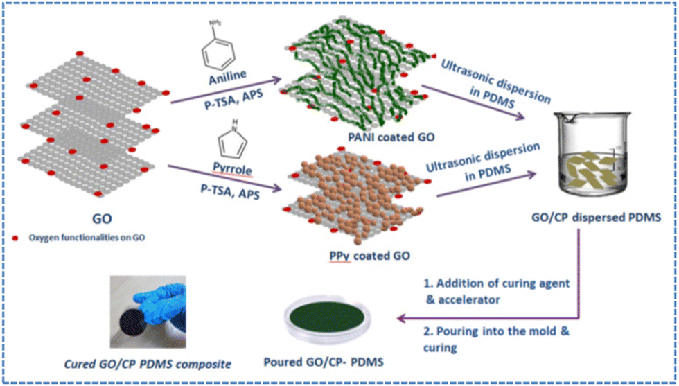 | ||
| Fig. 1 Schematic of the preparation of GO/CP PDMS composites. | ||
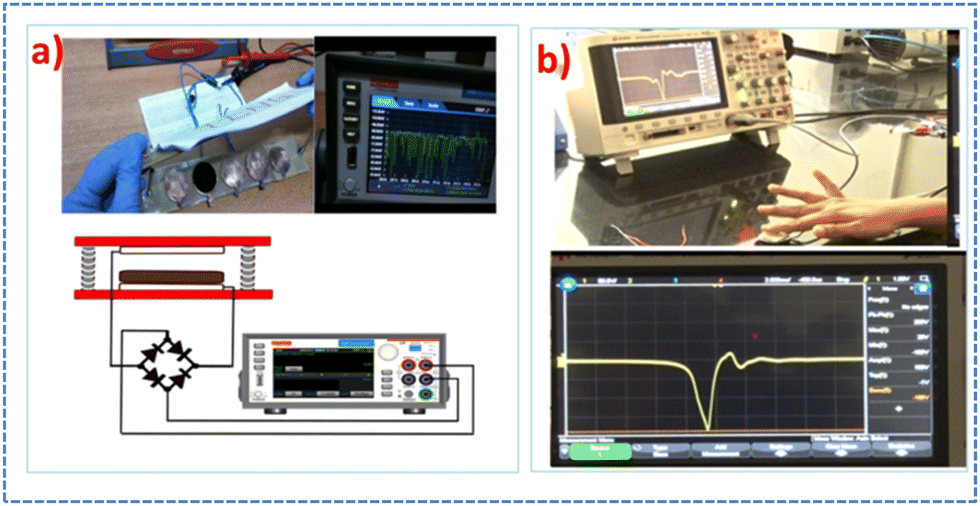
Setup for the measurement of TENG responses
Triboelectric power generation was analysed via the vertical-contact separation mode. In this work, a sewing machine was used to apply a constant external force of 5 N on the GO/CP-PDMS composites. For the triboelectric studies, samples of GO/CP-PDMS were cut into a circular piece of 3 cm diameter and sandwiched between two Cu foils of the same dimensions. In this mode, the dielectric material GO/CP-PDMS composite can act as the triboelectric surface, and the upper Cu electrode acts as the other triboelectric surface as well as the first contact electrode, while the bottom Cu electrode acts as the second contact electrode. The schematic of the preparation and testing of the samples is shown in Fig. 2.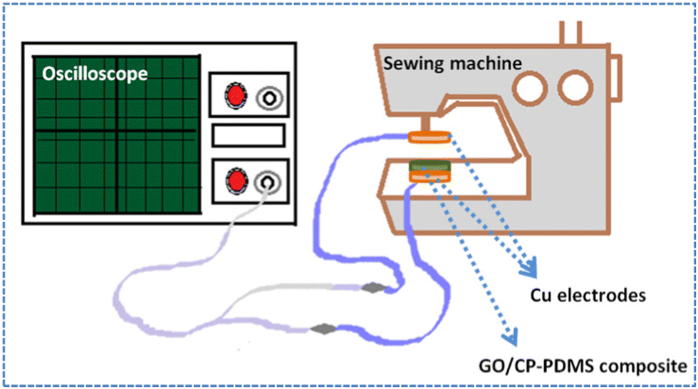 | ||
| Fig. 2 Custom designed set-up for the measurement of TENG performances. | ||
Characterisation
The Fourier transform infrared (FTIR) spectra of the powder samples of CPs and their GO hybrids were analyzed using a PerkinElmer Spectrum Two FTIR spectrometer using the KBr transmission mode in the wavenumber range of 400–4000 cm−1. The aqueous solution of samples at 0.01 mg ml−1 concentration was used for the ultraviolet-visible (UV-Vis) spectral analysis using an Elico 210 UV-visible spectrophotometer. Raman analysis of the powder samples was carried out using a WITEC Alpha 300 RA system excited at 532 nm. The powder morphology of the samples was analyzed using a JEOL 2100 transmission electron microscope (TEM). A Hitachi SU6600 variable pressure field emission scanning electron microscope (FE-SEM) was used for the surface morphology analyses of PDMS and PDMS composites. The elemental mapping analysis and the cross-sectional analyses of the PDMS composites were conducted using a JEOL 6390 SEM instrument. The dielectric constant of PDMS composites was measured using an Agilent 4294 A precision impedance analyzer in the range of 30 Hz to 30 MHz. The triboelectric voltage generation was analyzed with the help of a KEYSIGHT InfiniiVision DSOX3054T digital storage oscilloscope, and short circuit current and power were measured using a KEITHLEY 2450 source meter.Results and discussion
Structural and morphological analyses of GO and GO/CP hybrids
Structural characterization of the synthesized materials was done using FTIR spectroscopy. Fig. 3(a) shows the FTIR spectra of GO, CPs, and GO/CP hybrids. The modified Hummers’ method was used to oxidize the graphite powder, which resulted in the formation of exfoliated GO with hydroxyl, carboxylic, ether and epoxide groups in the basal plane and the edges.29 The FTIR spectrum of GO shows absorptions corresponding to C![[double bond, length as m-dash]](https://www.rsc.org/images/entities/char_e001.gif) O stretching (1733 cm−1), CC stretching (1609 cm−1), C–OH (1227 cm−1) and C–O–H stretching (1047 cm−1) vibrations in the material. The strong band at 3406 cm−1 is due to the stretching vibrations of the –OH bond present in the carboxylic acid group present in GO.30 The FTIR spectra of PANI and 1:4 GO:PANI show peaks corresponding to the C–H bending vibrations of the quinoid ring (∼1620 cm−1), CC stretching vibrations of the benzenoid ring (∼1490 cm−1), asymmetric C–N stretching (∼1295 cm−1) and –NH+ = stretching (1117 cm−1). Various physical interactions, such as electrostatic interactions, π–π stacking interactions, hydrogen bonding, etc., between GO and PANI led to peak shifts in the 1:4 GO:PANI hybrid compared to pristine PANI (green dotted lines, Fig. 3(a)). For instance, the peaks at 1621 cm−1, 1490 cm−1, 1298 cm−1, and 1117 cm−1 in PANI shifted to 1623 cm−1, 1470 cm−1, 1296 cm−1, and 1062 cm−1 in the 1:4 GO:PANI hybrid. A red shift of the benzenoid ring stretching and –NH+ = stretching peaks was evident in the FTIR spectra and this is due to the secondary interactions between PANI and GO.31
O stretching (1733 cm−1), CC stretching (1609 cm−1), C–OH (1227 cm−1) and C–O–H stretching (1047 cm−1) vibrations in the material. The strong band at 3406 cm−1 is due to the stretching vibrations of the –OH bond present in the carboxylic acid group present in GO.30 The FTIR spectra of PANI and 1:4 GO:PANI show peaks corresponding to the C–H bending vibrations of the quinoid ring (∼1620 cm−1), CC stretching vibrations of the benzenoid ring (∼1490 cm−1), asymmetric C–N stretching (∼1295 cm−1) and –NH+ = stretching (1117 cm−1). Various physical interactions, such as electrostatic interactions, π–π stacking interactions, hydrogen bonding, etc., between GO and PANI led to peak shifts in the 1:4 GO:PANI hybrid compared to pristine PANI (green dotted lines, Fig. 3(a)). For instance, the peaks at 1621 cm−1, 1490 cm−1, 1298 cm−1, and 1117 cm−1 in PANI shifted to 1623 cm−1, 1470 cm−1, 1296 cm−1, and 1062 cm−1 in the 1:4 GO:PANI hybrid. A red shift of the benzenoid ring stretching and –NH+ = stretching peaks was evident in the FTIR spectra and this is due to the secondary interactions between PANI and GO.31
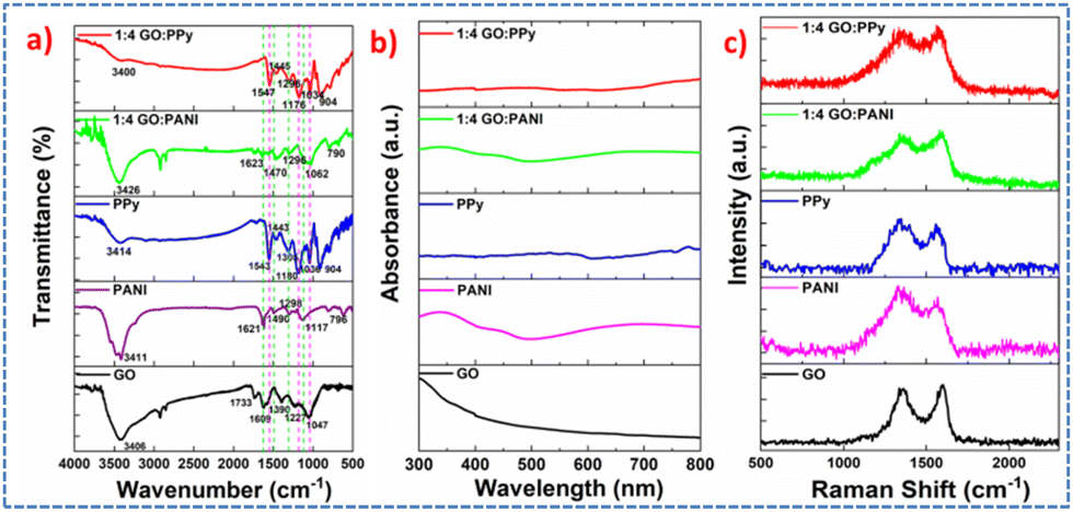 | ||
| Fig. 3 (a) FTIR spectra, (b) UV-Vis spectra and (c) Raman spectra of GO, PANI, PPy, 1:4 GO:PPy and 1:4 GO:PANI, respectively. | ||
In the spectrum of pristine PPy, the peaks at 1551 cm−1 and 1436 cm−1 correspond to the symmetric and anti-symmetric stretching of pyrrole rings. Also the peaks corresponding to the C–N stretching (1307 cm−1) and C–H deformation (1043 cm−1) of the doped PPy were observed. Similar to the 1:4 GO:PANI hybrid, a peak shift was observed in 1:4 GO:PPy compared to pristine PPy (pink dotted lines, Fig. 3(a)) due to the interaction between PPy and GO. The peaks at 1543 cm−1, 1305 cm−1, 1180 cm−1, and 1036 cm−1 in PPy shifted to 1547 cm−1, 1296 cm−1, 1176 cm−1, and 1034 cm−1 in the 1:4 GO:PPy hybrid. In GO/CP hybrids, the peaks corresponding to GO merged with the peaks of CPs due to their higher concentration.
UV-vis analysis was carried out to analyze the interfacial interaction of GO with PANI or PPy. Fig. 3(b) shows the UV-Vis spectra of samples in water at 0.01 mg ml−1 concentration. The aqueous solutions of pristine PANI and the 1:4 GO:PANI hybrid showed three characteristic absorption bands in the UV-Vis region around 375 nm and 455 nm and an extended absorption beyond 650 nm which are due to the π–π*, polaron–π* and π–polaron transitions in the emeraldine salt form of PANI.30,32,33 In pristine PPy and the 1:4 GO:PPy hybrid, the characteristic band due to the π–π* transition from the CC group of PPy was observed at 270 nm. Apart from this, a less intense peak below 400 nm due to the π–π* transition of the CN group of PPy was also observed.34 A broad and less intense peak due to bipolaron transitions in PPy was observed around 500 nm.35 Also, the formation of an oxidized form of PPy in pristine PPy and in the GO/PPy hybrid was evidenced by the appearance of a broad absorption beyond 600 nm.35
The Raman spectrum of GO (Fig. 3(c)) shows two major peaks at 1359 cm−1 and 1589 cm−1 which are designated as the D (defect) band and G (graphitic) band, respectively. In GO, due to the presence of oxygen functionalities and a partially disordered structure, the intensity of the D band is higher than that of the G band. The ID/IG value of 1.06 for GO indicates the increased sp3 carbon domain created due to the various functional groups in GO. However, the Raman analysis of GO/CP hybrids shows a decrease in the ID/IG value to 0.97 for 1:4 GO:PANI and to 0.94 for 1:4 GO:PPy. The shift in ID/IG from a higher to a lower value in hybrids indicates a partial repair of defects in GO sheets due to the hybridisation with PANI or PPy.36 An increased sp2 domain of carbon and extended conjugation of the hybrids resulted in the ID/IG ratio variation. Fig. 4 shows the TEM images of PPy, PANI, and the binary hybrids of PPy and PANI with GO. The TEM images clearly show the formation of PPy in nanospheres and PANI in nanofibers in the absence and presence of GO. Therefore, PPy nanosphere and PANI nanofiber intercalated GO morphologies were observed in GO/PPy and GO/PANI hybrids, respectively.
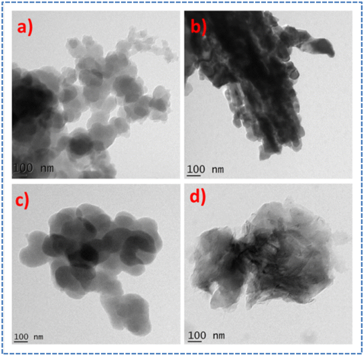 | ||
| Fig. 4 TEM images of (a) PPy, (b) PANI, (c) 1:4 GO:PPy and (d) 1:4 GO:PANI. | ||
Triboelectric properties of GO/CP-PDMS composites
PDMS composite sheets (GO/CP-PDMS) were cut into a specific size and sandwiched between two copper electrodes for triboelectric studies in the vertical contact separation mode by applying an external force of 5 N at a frequency of 5 Hz using the set-up depicted in Fig. 2. The energy harvester proposed in this work is prepared as follows.The PDMS composite was prepared by adding fillers to the bulk of the PDMS matrix and sandwiched it between two Cu electrodes. The bulk modified PDMS sheet acts as the tribonegative layer, while the upper electrode serves as the tribopositive layer and the second contact electrode. An external vertical force of 5 N at a frequency of 5 Hz was applied with the help of a custom-built set-up (sewing machine), and the triboelectric responses were analyzed in the vertical-contact separation mode. Fig. 5 shows the mechanism of triboelectric charge generation in the proposed system explained with the 1:4 GO:PANI-PDMS composite as an example. Initially, there is no charge transfer or power generation in the system because the top Cu plate is not in contact with the triboelectric material (PDMS or PDMS composites). When the top (Cu) and the bottom (PDMS composite) electrodes have come into contact, positive charges will develop on the Cu electrode and negative charges on composite materials due to the triboelectric effect. This charge flow makes the Fermi levels of the two materials coincide according to the surface state model for metal–polymer contact charging. However, a separation between triboelectric materials will induce an electric field on both electrodes, resulting in a potential difference across the electrodes. Therefore, electrons will flow from the bottom electrode to the top electrode to balance the potential difference until the potential drop becomes zero. Similarly, when the top electrode is pressed onto the bottom electrode (triboelectric material and Cu), a potential drop arises again due to varying induced electric fields. So, to balance the potential difference, electrons will start to flow from the top to the bottom electrode. Thus, a periodic application and removal of a constant force will generate positive and negative charge pulses in the system.
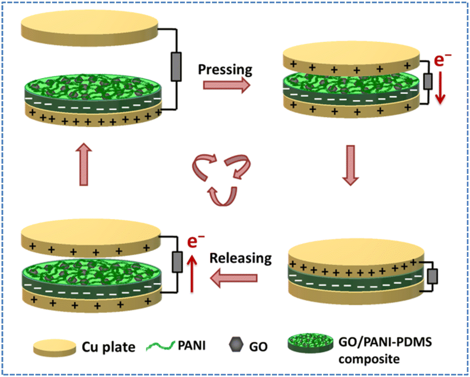 | ||
| Fig. 5 Working mechanism of the TENG. | ||
Triboelectric responses such as open-circuit voltage and short circuit current and charge waveforms of bare PDMS sheet and its various composites with 0.5 wt% fillers (GO, CP, and GO/CP hybrids) are shown in Fig. 6–8, respectively, and the values are tabulated in Table 2. The triboelectric properties of all PDMS composites were found to be higher than those of neat PDMS. In GO-PDMS, GO with sheet-like structures and wrinkles can act as charge trapping sites. Also, it may serve as a negative triboelectric material due to the high electron affinity of oxygen functionalities present in it.17,20 Therefore, the GO incorporated PDMS composite sheets can experience enhanced surface charges or intensified negative charges during the triboelectric charge generation process, resulting in better TENG performances. For instance, the open-circuit voltage of GO-PDMS was 8.14 V and the short circuit current was 88.5 nA, and these were higher than those of a neat PDMS sheet (an open-circuit voltage of 6.6 V and a short circuit current of 55 nA as depicted in Fig. 6). An increase in the dielectric constant was observed for the GO-PDMS composite (4.7) as compared to neat PDMS (3.5) which could be another reason for better TENG outputs of the GO-PDMS sheet (Fig. 9). GO in the PDMS could act as charge trapping centers, thereby enhancing the TENG performances.17,18,37
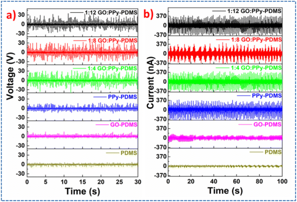 | ||
| Fig. 6 (a) Open circuit voltage and (b) short circuit current of PDMS, GO-PDMS and GO/PPy-PDMS composites. | ||
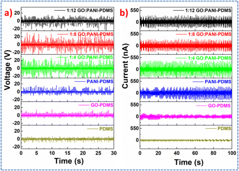 | ||
| Fig. 7 (a) Open circuit voltage and (b) short circuit current of PDMS, GO-PDMS and GO/PANI-PDMS composites. | ||
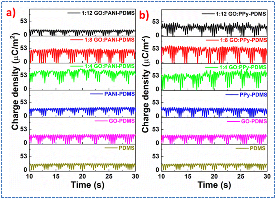 | ||
| Fig. 8 Charge waveforms of TENGs with PDMS and various (a) PANI based fillers and (b) PPy based fillers. | ||
| Sample name | Open-circuit voltage (V) | Short circuit current (nA) | Current density (mA m−2) |
|---|---|---|---|
| PDMS | 6.6 | 55 | 0.078 |
| GO-PDMS | 8.14 | 88.5 | 0.126 |
| PPy-PDMS | 12.4 | 288 | 0.502 |
1![[thin space (1/6-em)]](https://www.rsc.org/images/entities/b_char_2009.gif) :4 GO:PPy-PDMS :4 GO:PPy-PDMS |
27 | 354 | 0.501 |
| 1:8 GO:PPy-PDMS |
26.5 | 336 | 0.476 |
| 1:12 GO:PPy-PDMS |
25.99 | 337 | 0.477 |
| PANI-PDMS | 11 | 254 | 0.36 |
|
1:4 GO:PANI-PDMS |
23.88 | 364 | 0.515 |
| 1:8 GO:PANI-PDMS |
19.55 | 266 | 0.377 |
| 1:12 GO:PANI-PDMS |
13.12 | 322 | 0.456 |
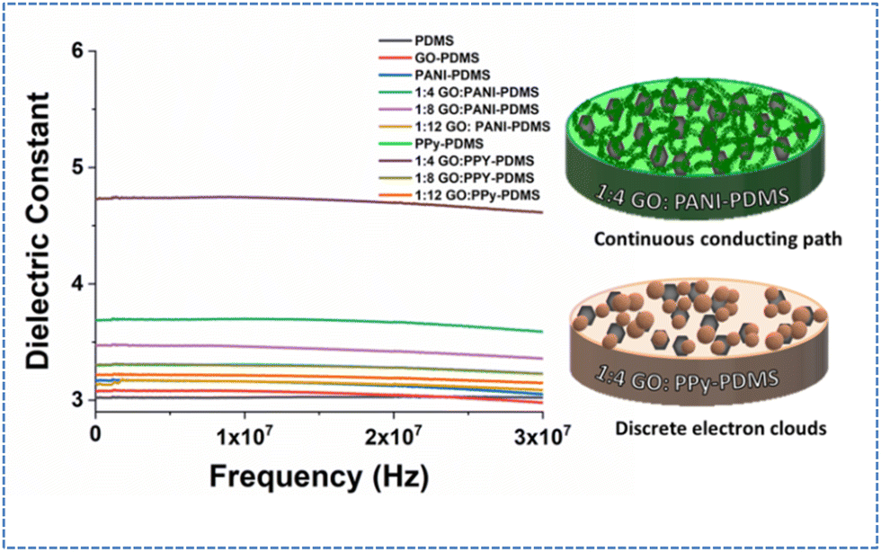 | ||
| Fig. 9 (a) Dielectric constants of PDMS and PDMS composites, (b) schematic of the representation of discrete electron clouds formed in GO/PPy and (c) continuous conducting network formed in the GO/PANI hybrid. | ||
Further, the triboelectric responses of PDMS composites prepared by introducing binary hybrids of GO with CP (PPy and PANI) into the PDMS matrix were analyzed. The incorporation of GO/PPy or GO/PANI into PDMS has further enhanced the triboelectric responses of the composites as compared to neat PDMS or GO-PDMS sheets. PPy or PANI intercalated GO sheets were introduced into the PDMS matrix via the ultrasonication-assisted dispersion method. The hybrids formed may act as charge trapping sites due to electron-donating PPy or PANI chains and the electron-accepting oxygen functionalities in GO. Therefore, the increased charge density in the bulk and surface of the PDMS composite can lead to an enhanced TENG output. GO:PPy-PDMS composites with various ratios of 1:4, 1:8, and 1:12 were prepared and the 1:4 GO:PPy-PDMS composite showed an open-circuit voltage and short circuit current of 27 V and 354 nA, respectively. These values were higher as compared to 1:8 GO:PPy (the open circuit voltage was 26.5 V and the short circuit current was 336 nA) and 1:12 GO:PPy hybrids (the open circuit voltage was 25.9 V and the short circuit current was 337 nA). The decreased amounts of GO in the hybrid can affect the electron donation/acceptance mechanism in the hybrids and can lead to a decrease in the overall charge density and TENG performances of the PDMS composites. The charge trapping centres developed due to the introduction of GO will be less in these composites and can result in a reduction in TENG performances. Also, the addition of a high concentration of conducting PPy as in 1:8 GO:PPy and 1:12 GO:PPy can generate more conducting paths inside the composite. The formation of a high amount of conducting network can be neutralized by the triboelectric charges formed in the PDMS composite which may decrease the output performance by decreasing the surface charges in the system.25
Similar to the triboelectric studies on GO/PPy-PDMS composites, the TENG performances of GO:PANI-PDMS composite sheets were also analyzed. As in the case of GO PPy-PDMS composites, the 1:4 GO:PANI-PDMS composite (the open circuit voltage was 23.6 V and the short circuit current was 364 nA) showed better TENG performances than 1:8 GO:PANI-PDMS (the open circuit voltage was 19.55 V and the short circuit current was 266 nA) and 1:12 GO:PANI-PDMS composites (the open circuit voltage was 13.12 V and the short circuit current was 322 nA). The electron-donating nature of PANI and the electron-accepting nature of GO could effectively enhance the surface charges in the PDMS composite. Further, the improvement in the dielectric properties of PDMS after the incorporation of the binary hybrids can help to improve the TENG properties. The charge trapping centers developed in the system are one of the primary reasons for the property enhancement.
The charge density waveforms of PDMS and PDMS composites presented in Fig. 8 show a similar trend to voltage and current outputs. The charge density of the bare PDMS was increased from 23.2 μC m−2 to 69.5 μC m−2 in 1:4 GO:PPy-PDMS due to the incorporation of the 1:4 GO:PPy filler into the PDMS matrix.
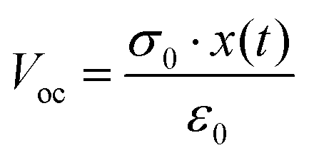
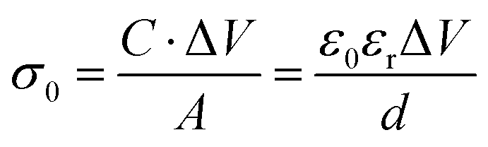
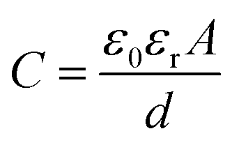
The open circuit potential (Voc) of a TENG is given by38,39
 | (1) |
From these inferences, it was reported that38,39
 | (2) |
 | (3) |
From eqn (1)–(3), we can understand that Voc is directly proportional to charge density, and the capacitance is directly proportional to the dielectric constant. Therefore, as per eqn (2) and (3), with an increase in the dielectric constant, the capacitance and charge density of the material can be enhanced, which leads to an improved Voc of the material. These inferences could correlate with the observed TENG output and dielectric constant measured (Fig. 9). Of these different PDMS composites, 1:4 GO:PPy-PDMS with the highest dielectric constant value showed the highest open-circuit voltage of 27 V under constant contact and separation using the sewing machine.
The TEM studies showed that the morphologies of PANI and PPy formed by oxidative chemical polymerization are nanofibers and nanospheres, respectively, as shown in Fig. 4. The binary hybrids of GO and PANI showed nanofiber intercalated GO nanosheet morphology, while that of GO and PPy showed nanosphere intercalated GO nanosheet morphology (Fig. 4(b and c)). Since PANI is in the fiber form, the conducting paths developed between polymer chains and GO sheets will be more effective in GO/PANI hybrids than in GO/PPy hybrids. Hence the GO:PANI-PDMS composite shows a higher short circuit current than the GO:PPy-PDMS composite. The GO/CP hybrid modified tribonegative PDMS offers a new mechanism for the property enhancement. Upon dispersing tribopositive GO/CP hybrids, the electrons donated from CPs will be accepted by tribonegative GO and PDMS, leading to enhanced charge transfer and high surface charge density in the system. Due to the formation of sufficient amounts of conducting paths in 1:4 GO:PANI-PDMS via the nanofiber intercalated GO morphology of the incorporated binary hybrids, a facile charge transfer in the composite will result in the generation of a higher short circuit current during the energy harvesting process.
To further illustrate the energy harvesting property enhancement mechanism in PDMS composites, the dielectric properties of the samples were analyzed over the frequency range of 30 Hz to 30 MHz at room temperature. The dielectric constants of the PDMS composites are depicted in Fig. 9. Conducting polymers consist of crystalline regions with amorphous barriers, and charge accumulation at the interfaces of amorphous and crystalline regions yields higher dielectric properties.31 By incorporating GO in PANI or PPy, besides the doping-induced polarization of doped CPs, filler-induced interfacial polarization may also contribute to the dielectric properties. Further, the difference in the electrical properties of GO and CPs resulted in the formation of a heterogeneous system, leading to charge localization at interfaces via the Maxwell–Wagner–Sillars interfacial polarization phenomenon.40 The dielectric constant of neat PDMS increased from 3.5 to 4.6 by incorporating 0.5 wt% of the 1:4 GO:PPy filler into the PDMS matrix. The PDMS composite prepared by the addition of 1:4 GO:CP showed better dielectric properties when compared to other PDMS composites. The enhanced dielectric constant in 1:4 GO:CP-PDMS composites is due to the higher amount of GO present compared to other composites (with 1:8 GO:CP and 1:4 GO:CP fillers). The formation of more heterogeneous interfaces in 1:4 GO:CP-PDMS leads to additional interfacial polarization and enhanced dielectric properties.
The higher dielectric constant of the 1:4 GO:PPy-PDMS composite compared to 1:4 GO:PANI-PDMS evidenced the high capacitive nature of the 1:4 GO:PPy-PDMS composite. PPy nanospheres intercalated with GO sheets form a 3D network-like structure and they can act as charge trapping sites in PDMS due to the electron-donating nature of the nitrogen atoms and the electron-accepting nature of the oxygen functionalities in GO. Due to the decreased or inefficient electron transferring-conducting paths in GO/PPy compared to GO/PANI, electron clouds can persist in the GO/PPy structure itself, resulting in a more capacitive nature of the system. Since the voltage generation is as per the charge accumulation, the material with more electron clouds can deliver a high open-circuit voltage. Therefore, the 1:4 GO:PPy-PDMS composite with more capacitive nature resulted in an increased open-circuit voltage. The dielectric constant measurement results are in good agreement with the TENG output as described in eqn (1)–(3).
The SEM images of the neat PDMS, 1:4 GO:PPy-PDMS and 1:4 GO:PANI-PDMS films are shown in Fig. 10(a–c), respectively. A neat PDMS film with very smooth surface morphology is evidenced from Fig. 10(a). Even after the dispersion of GO:PPy or GO:PANI binary hybrids, a smooth surface of the PDMS composite was observed as shown in Fig. 10(b and c) and this infers the uniform dispersion of the filler in the matrix. The cross-sectional view shown in Fig. 10(c and d) reveals the presence of dispersed GO:PPy and GO:PANI nanohybrids in the PDMS matrix. The chemical composition of the surface of the composite was investigated by using energy dispersive X-ray spectroscopy (EDS). The elemental mapping profiles of the 1:4 GO:PANI-PDMS composite prepared by the addition of the 0.5 wt% 1:4 GO:PANI filler in the PDMS matrix are shown in Fig. 11. The exposed surface is composed of S, C, N, O, and Si which includes in the composite film. The presence of the uniformly dispersed filler in the matrix is supported by the images shown in Fig. 11.
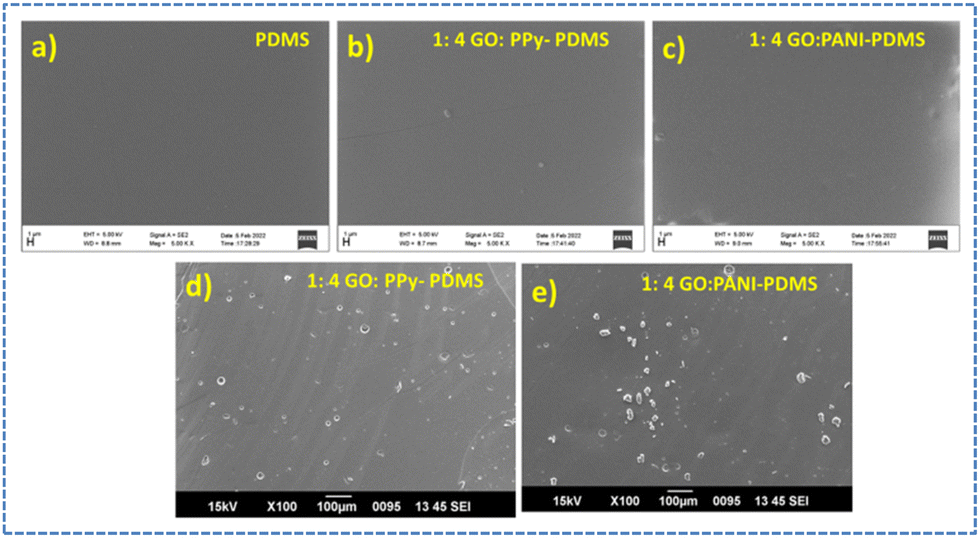 | ||
| Fig. 10 SEM images of the surface of PDMS (a); 1:4 GO:PPy-PDMS (b); and 1:4 GO:PANI-PDMS (c). SEM images of the cross section of 1:4 GO:PPy-PDMS and (d) 1:4 GO:PANI-PDMS (e). | ||
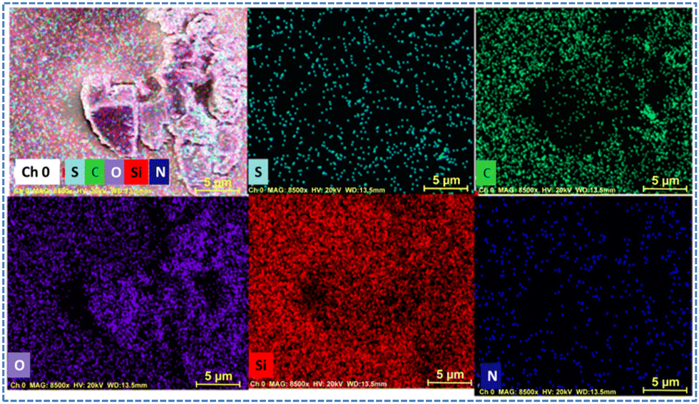 | ||
| Fig. 11 Elemental mapping images of 1:4 GO:PANI-PDMS. | ||
The studies reported in this paper suggest that the TENG based on the GO/CP-PDMS composite showed superior performance to neat PDMS due to the following reasons: (1) an enhancement in the dielectric constant of PDMS composites led to an improved surface charge density, which resulted in significant voltage and current generation. The change in the dielectric properties of the PDMS composite was achieved by various phenomena such as dielectric and interfacial polarization. (2) The electron donating–accepting process between PDMS and the GO/CP filler enhances the surface charge density and overall TENG performance of the PDMS composite. (3) In the case of the GO: PANI-PDMS composite, the nanofiber intercalated GO morphology of the GO/PANI hybrid in the PDMS composite resulted in a better current generation when compared to PPy nanosphere intercalated GO incorporated PDMS system.
Role of the filler and energy harvesting studies
The material with a high short circuit current was selected to study the effect of the filler in the PDMS matrix. Therefore, the PDMS composite with the 1 wt% 1:4 GO:PANI filler was prepared, and the triboelectric responses were measured. The samples prepared had the same dimensions, and the TENG measurement was conducted under a periodic compressive force of 5 N at a frequency of 5 Hz. The short-circuit current and open-circuit voltage were found to be 387 nA and 25.28 V, respectively, which were higher than those of the PDMS composite with 0.5 wt% of the 1:4 GO:PANI filler. Due to the improper dispersion of 1.5 wt% filler in the PDMS matrix, the energy harvesting studies were carried out using PDMS composites with 1 wt% 1:4 GO:PANI filler.
The circular sample with a 3 cm diameter of the 1:4 GO:PANI-PDMS composite was placed between two copper electrodes. One electrode is attached to a piece of hardboard using an insulation tape for a firm attachment. Two copper wires were used as the lead to the source meter or oscilloscope to measure the current and voltage generated in the system. Upon a single finger tapping on the top of the hardboard, a current of 40 nA and a voltage of 208 V were generated as depicted in Fig. 12(a and b). A video file showing the energy harvesting ability of the proposed TENG by simple body movements is given in the supporting information (SV1). Further, the energy harvesting capability of the proposed material was demonstrated by utilizing the mechanical energy harvested from human walking or foot stamping. For this, the 1:4 GO:PANI-PDMS composite sheet was sandwiched between two conducting cloths and the whole set-up was wrapped with a Kapton tape after attaching the electrical leads as depicted in Fig. 13(a). The as-prepared TENG module was affixed under the shoes using a double-sided tape as shown in Fig. 13(b). The voltage and current generated by human walking were measured using the source meter/oscilloscope connected to the TENG module under the shoes through the electrical leads. An average current and voltage of about 2.5 μA and 27 V were obtained by foot stamping (Fig. 13(c)). A video file showing current and voltage generation while walking using the proposed system is given in the supporting information (SV2). The energy harvesting capacity of the proposed composite material (1:4 GO:PANI-PDMS) was compared with the bare PDMS film. The voltage and current generated in bare PDMS were 1 μA and 5 V, which increased up to 2.5 μA and 27 V for the 1:4 (GO:PANI) incorporated PDMS composite. We have already observed the ability to have a better TENG output for the filler added PDMS composite than the bare one under constant contact and separation using the sewing machine (in Fig. 6–8). Likewise, under continuous walking, a higher short-circuit current and open-circuit voltage were observed for the filler added PDMS system as compared to the bare PDMS sheet. The significant reasons for the enhanced TENG output in filler added PDMS were the enhanced dielectric constant of PDMS, the electron donor–acceptor process between PDMS and the GO/CP filler, and the presence of electron trapping conducting polymer-coated GO centers within the PDMS matrix. The aforementioned reasons for the enhanced TENG output by the composite material were validated via different characterization techniques described in the previous sections of the manuscript. The studies reported in this paper hint at the utility of the proposed PDMS composite material for mechanical energy harvesting using simple body movements.
 | ||
| Fig. 12 Energy harvesting studies demonstrated using the 1:4 GO:PANI-PDMS composite. (a) Current and (b) voltage generation by the 1:4 GO:PANI-PDMS composite upon finger tapping. | ||
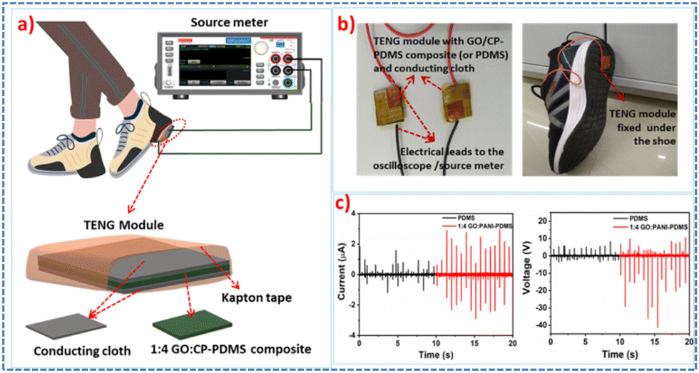 | ||
| Fig. 13 (a) Schematic of the proposed TENG as an energy harvesting material when placed under the shoes; (b) photographs of the TENG modules prepared using GO/CP-PDMS (or PDMS) and conducting cloth as the electrode and the TENG module attached shoes; (c) current and voltage generated by walking using bare PDMS and 1:4 GO:PANI-PDMS as the triboelectric material. | ||
Conclusions
To conclude, a TENG was developed for mechanical energy harvesting by a simple ultrasonication assisted incorporation of binary hybrids of GO and the conducting polymer PANI or PPy in the PDMS matrix at room temperature. An improvement in the dielectric properties of PDMS composites by incorporating 0.5 wt% GO/CP was found to be an efficient method to enhance the TENG performance of neat PDMS. Tuning of the dielectric constant of the PDMS composite led to an improved surface charge density in the PDMS composite, which resulted in a significant voltage and current generation in 1:4 GO:PPy-PDMS (27 V, 354 nA (0.501 mA m−2)) and in 1:4 GO:PANI-PDMS (23.88 V and 364 nA (0.515 mA m−2)) composites. Also, the GO and CP ratios in the binary hybrids change the dielectric properties of the PDMS composite by various phenomena such as dielectric polarization (which includes electronic, vibrational, orientation, and ionic) and interfacial polarization. Other than the improved dielectric properties of the PDMS composite, the electron donating–accepting process between PDMS and the GO/CP filler enhances the surface charge density and overall TENG performances of the conducting polymer incorporated PDMS composite. Further, the morphology of GO/CP binary hybrids is a crucial factor in deciding the TENG performances. The PANI nanofiber intercalated GO morphology of the GO/PANI hybrid in the PDMS composite resulted in a better current generation when compared to the PPy nanosphere intercalated GO incorporated PDMS system. Therefore, the superior performances of GO/CP-PDMS composites compared to neat PDMS are attributed to the intensified negative charges on PDMS from the functional groups of GO, PANI, or PPy chains and the enhanced dielectric properties. The energy harvesting studies using the PDMS composites were demonstrated using various body movements such as single finger tapping and foot stamping. A current of 40 nA and a voltage of 208 V were generated by finger tapping, whereas a short circuit current of 2.5 μA and a voltage of 27 V were generated by walking. These studies hint at the utility of the proposed material for mechanical energy harvesting using simple body movements.
Author contributions
Jelmy E. J. and Divya Jose made equal contributions to the work reported in this manuscript. The conceptualization, design of the experiments, overall supervision of the studies undertaken, and the manuscript correction were done by Dr Honey John. Preparation of the samples, characterization, acquisition of data, and manuscript preparation were done by Dr Jelmy E. J. and Dr Divya Jose. K. V Vijoy prepared the set-up for energy harvesting applications. Dr K. J Saji performed the supervision of the TENG studies.Part of the work described in this paper has been filed for an Indian patent with application number 202141021948 dated on 15th May, 2021.
Conflicts of interest
The authors listed in the manuscript have no affiliations with or involvement in any organization or entity with any financial interest or non-financial interest in the subject matter or materials discussed in this manuscript and hereby we declare there is no conflict of interest.Acknowledgements
The authors acknowledge Sophisticated Test & Instrumentation Centre (STIC), Cochin University of Science and Technology for the different characterisations of the samples. K. V. Vijoy acknowledges the Ministry of New & Renewable Energy (MNRE), India for the fellowship.Notes and references
- Y. Song, H. Wang, X. Cheng, G. Li, X. Chen, H. Chen, L. Miao, X. Zhang and H. Zhang, Nano Energy, 2019, 55, 29–36 CrossRef CAS.
- C. Yan, Y. Gao, S. Zhao, S. Zhang, Y. Zhou, W. Deng, Z. Li, G. Jiang, L. Jin, G. Tian, T. Yang, X. Chu, D. Xiong, Z. Wang, Y. Li, W. Yang and J. Chen, Nano Energy, 2020, 67, 104235 CrossRef CAS.
- A. Libanori, Research, 2020, 2020 Search PubMed.
- R. Zhang and O. Amft, IEEE J. Biomed. Health Inform., 2018, 22, 23–32 Search PubMed.
- Z. Lin, J. Yang, X. Li, Y. Wu, W. Wei and J. Liu, Adv. Funct. Mater., 2017, 28 CAS.
- B. Dudem, A. Mule, H. Patnam and J. Yu, Nano Energy, 2018, 55 Search PubMed.
- Y. Zou, J. Xu, K. Chen and J. Chen, Adv. Mater. Technol., 2021, 6, 2000916 CrossRef CAS.
- F.-R. Fan, Z.-Q. Tian and Z. Lin Wang, Nano Energy, 2012, 1, 328–334 CrossRef CAS.
- W.-G. Kim, D.-W. Kim, I.-W. Tcho, J.-K. Kim, M.-S. Kim and Y.-K. Choi, ACS Nano, 2021, 15, 258–287 CrossRef CAS PubMed.
- C. Wu, A. C. Wang, W. Ding, H. Guo and Z. L. Wang, Adv. Energy Mater., 2019, 9, 1802906 CrossRef.
- A. Chen, C. Zhang, G. Zhu and Z. L. Wang, Adv. Sci., 2020, 7, 2000186 CrossRef CAS PubMed.
- Y. Liu, J. Ping and Y. Ying, Adv. Funct. Mater., 2021, 31, 2009994 CrossRef CAS.
- Y. Zhou, W. Deng, J. Xu and J. Chen, Cell Rep. Phys. Sci., 2020, 1, 100142 CrossRef CAS.
- X. He, H. Guo, X. Yue, J. Gao, Y. Xi and C. Hu, Nanoscale, 2015, 7, 1896–1903 RSC.
- S. Jang and J. H. Oh, Sci. Rep., 2018, 8, 14287 CrossRef PubMed.
- B. Yang, W. Zeng, Z.-H. Peng, S.-R. Liu, K. Chen and X.-M. Tao, Adv. Energy Mater., 2016, 6, 1600505 CrossRef.
- V. Harnchana, H. V. Ngoc, W. He, A. Rasheed, H. Park, V. Amornkitbamrung and D. J. Kang, ACS Appl. Mater. Interfaces, 2018, 10, 25263–25272 CrossRef CAS PubMed.
- A. N. Parvez, M. H. Rahaman, H. C. Kim and K. K. Ahn, Composites, Part B, 2019, 174, 106923 CrossRef CAS.
- Y. Liu, Y. Zheng, Z. Wu, L. Zhang, W. Sun, T. Li, D. Wang and F. Zhou, Nano Energy, 2021, 79, 105422 CrossRef CAS.
- R. u S. Ahmad, A. Haleem, Z. Haider, U. P. Claver, A. Fareed, I. Khan, M. K. Mbogba, K. Memon, W. Ali, W. He, P. Hu and G. Zhao, Adv. Electron. Mater., 2020, 6, 2000034 CrossRef CAS.
- C. Wu, T. W. Kim and H. Y. Choi, Nano Energy, 2017, 32, 542–550 CrossRef CAS.
- J. H. Choi, Y. Ra, S. Cho, M. La, S. J. Park and D. Choi, Compos. Sci. Technol., 2021, 207, 108680 CrossRef CAS.
- J. Chen, H. Guo, X. He, G. Liu, Y. Xi, H. Shi and C. Hu, ACS Appl. Mater. Interfaces, 2015, 8, 736–744 CrossRef PubMed.
- Y. J. Fan, X. S. Meng, H. Y. Li, S. Y. Kuang, L. Zhang, Y. Wu, Z. L. Wang and G. Zhu, Adv. Mater., 2017, 29, 1603115 CrossRef PubMed.
- Z. Liu, M. Muhammad, L. Cheng, E. Xie and W. Han, Appl. Phys. Lett., 2020, 117, 143903 CrossRef CAS.
- X. Xia, J. Chen, G. Liu, M. S. Javed, X. Wang and C. Hu, Carbon, 2017, 111, 569–576 CrossRef CAS.
- T. Remyamol, H. John and P. Gopinath, Carbon, 2013, 59, 308–314 CrossRef CAS.
- D. Jose, E. J. Jelmy, P. S. Subin, R. Joseph and H. John, J. Mater. Sci.: Mater. Electron., 2022, 33, 15408–15421 CrossRef CAS.
- A. Kaniyoor, T. T. Baby and S. Ramaprabhu, J. Mater. Chem., 2010, 20, 8467–8469 RSC.
- S. Goswami, U. N. Maiti, S. Maiti, S. Nandy, M. K. Mitra and K. K. Chattopadhyay, Carbon, 2011, 49, 2245–2252 CrossRef CAS.
- E. J. Jelmy, S. Ramakrishnan and N. K. Kothurkar, Polym. Adv. Technol., 2016, 27, 1246–1257 CrossRef CAS.
- G. Xu, N. Wang, J. Wei, L. Lv, J. Zhang, Z. Chen and Q. Xu, Ind. Eng. Chem. Res., 2012, 51, 14390–14398 CrossRef CAS.
- Y.-W. Lin and T.-M. Wu, Compos. Sci. Technol., 2009, 69, 2559–2565 CrossRef CAS.
- S. Yalçınkaya and D. Çakmak, Hacettepe J. Biol. Chem., 2016, 44, 425–434 Search PubMed.
- M. Choudhary, R. U. Islam, M. J. Witcomb and K. Mallick, Dalton Trans., 2014, 43, 6396–6405 RSC.
- R. Thekkayil, P. Gopinath and H. John, Mater. Res. Express, 2014, 1, 035051 CrossRef.
- T. Huang, M. Lu, H. Yu, Q. Zhang, H. Wang and M. Zhu, Sci. Rep., 2015, 5, 13942 CrossRef CAS PubMed.
- S. M. S. Rana, M. T. Rahman, S. Sharma, M. Salauddin, S. H. Yoon, C. Park, P. Maharjan, T. Bhatta and J. Y. Park, Nano Energy, 2021, 88, 106300 CrossRef CAS.
- T. Bhatta, P. Maharjan, H. Cho, C. Park, S. H. Yoon, S. Sharma, M. Salauddin, M. T. Rahman, S. M. S. Rana and J. Y. Park, Nano Energy, 2021, 81, 105670 CrossRef CAS.
- M. Devi and A. Kumar, J. Appl. Polym. Sci., 2018, 135, 45883 CrossRef.
Footnote |
| † Electronic supplementary information (ESI) available: A video file showing the energy harvesting ability of the proposed TENG by simple body movements (SV1). A video file showing current and voltage generation while walking using the proposed system has been given in SV2. See DOI: https://doi.org/10.1039/d2ma00771a |
| This journal is © The Royal Society of Chemistry 2022 |