
 Open Access Article
 This Open Access Article is licensed under a Creative Commons Attribution-Non Commercial 3.0 Unported Licence
Ion-irradiation of catalyst and electrode materials for water electrolysis/photoelectrolysis cells, rechargeable batteries, and supercapacitors
Yahui
Wang
 a,
Xing
Cheng
a,
Kai
Zhang
b,
Ge
Chen
*a,
Ruzhi
Wang
*c and
Jiujun
Zhang
*d
a,
Xing
Cheng
a,
Kai
Zhang
b,
Ge
Chen
*a,
Ruzhi
Wang
*c and
Jiujun
Zhang
*d
aBeijing Key Laboratory for Green Catalysis and Separation, Faculty of Environment and Life, Beijing University of Technology, Beijing, 100124, China. E-mail: chenge@bjut.edu.cn
bThe College of Architecture and Civil Engineering, Beijing University of Technology, Beijing, 100124, China
cInstitute of New Energy Materials and Devices, Faculty of Materials and Manufacturing, Key Laboratory of Advanced Functional Materials of Education Ministry of China, Beijing University of Technology, Beijing 100124, China. E-mail: wrz@bjut.edu.cn
dInstitute for Sustainable Energy, College of Sciences, Shanghai University, Shanghai, 200444, China. E-mail: jiujun@i.shu.edu.cn
First published on 9th August 2022
Abstract
Innovatively designed, modified, and synthesized catalyst/electrode materials are of great importance in improving the performance of electrochemical energy devices for energy storage and conversion. Among various material modification technologies, the ion-irradiation technique has been recognized as a promising technology, which can effectively modify and design materials through controlling the key irradiation parameters, such as irradiation ion species, energy and fluence. The advantages of the ion-irradiation technique are high precision, favorable controllability, favorable repeatability, etc.; meanwhile, it can realize arbitrary element doping and defect control for many catalyst/electrode materials. Notably, it does not induce any impurities into the target materials during the ion-irradiation process, which is superior to many chemical modifications. The effects of ion-irradiation on catalyst/electrode materials in recent years are described in this review, including defect introduction, regulation of the electronic structure, morphology control, synthesis, and element doping. Then, the applications of ion irradiated catalyst/electrode materials in water electrolysis/photoelectrolysis cells, lithium-ion batteries, and supercapacitors are systematically summarized with an emphasis on the advantages of boosting the properties of materials. Finally, the challenges and strategies are proposed for developing more practical ion-irradiation techniques towards high-performance catalyst/electrode materials.
 Yahui Wang | Yahui Wang is currently a PhD candidate under the supervision of Prof. Ge Chen in the Faculty of Environment and Life, Beijing University of Technology. She received her Master's degree from Lanzhou Jiaotong University in 2019. Her current research interests focus on the electrochemical production of hydrogen peroxide. |
 Xing Cheng | Xing Cheng is currently a PhD candidate under the supervision of Prof. Ge Chen in the Faculty of Environment and Life, Beijing University of Technology. She received her Master's degree (2018) from the Beijing University of Technology. Her research interests mainly focus on designing atomically dispersed electrocatalysts. |
 Kai Zhang | Kai Zhang is currently a PhD candidate in the College of Architecture and Civil Engineering, Beijing University of Technology. He received his Master's degree from the Hebei University of Engineering in 2018. His current research interests focus on advanced oxidized water treatment technologies and emerging pollutant control technologies. |
 Ge Chen | Ge Chen received his BS and MS degrees from the University of Science & Technology, Beijing, in 1997 and 2000, respectively, and PhD degree from the Beijing University of Technology in 2010. He is now a full professor in the Faculty of Environment and Life, Beijing University of Technology. His research group interests are focused on developing novel electrocatalysts towards energy conversion. |
 Ruzhi Wang | Ruzhi Wang received his BS and MS degrees from Xiangtan University in 1997 and 2000, respectively, and his PhD degree from the Beijing University of Technology in 2003. He is now a full professor and director at the Institute of New Energy Materials and Devices in Faculty of Materials and Manufacturing, Beijing University of Technology. His research focuses on the design, fabrication, and device applications of novel semiconductor optoelectronic functional materials and new energy materials. |
 Jiujun Zhang | Jiujun Zhang is a Professor in the College of Sciences/Institute for Sustainable Energy at Shanghai University, and a former Principal Research Officer (Emeritus) at the National Research Council of Canada (NRC). Dr Zhang received his BS and MSc degrees in Electrochemistry from Peking University in 1982 and 1985, respectively, and his PhD degree in Electrochemistry from Wuhan University in 1988. Dr Zhang's expertise areas are electrochemistry, electrocatalysis, fuel cells, batteries, supercapacitors, and water/CO2 electrolysis. |
Introduction
In an effort to decrease the depletion rate of fossil fuels and reduce the associated environmental impact, exploring clean and sustainable energy sources such as solar, wind, waterfall, etc. for generating clean electrical energy has become imperative in recent years. However, such electricity is intermittent, and highly efficient energy storage and conversion technologies are needed to make them suitable for many applications.1,2 In this regard, electrochemical energy devices such as rechargeable batteries, supercapacitors, and water electrolysis cells have been recognized as the reliable, efficient, and practical means to meet the renewable energy storage and conversion requirement. Achieving higher energy/power densities, lifetime, and safety of these devices are always the relentless pursuit,3,4 and the development of highly efficient catalyst/electrode materials has been the major focus, which can be approached through innovative design and fabrication as well as modification for the device performance optimization.5–7 Particularly, elaborately modified catalyst/electrode materials are believed to be one of the most efficient ways of obtaining high performance.8,9Among various modification strategies, ion-irradiation has been identified as an environmentally friendly technique that can modify the material without using any chemical reagents. When the energy of ion irradiation is large enough, it is able to transfer considerable energy and momentum to a single atom or an electron. This is also the main reason why ion-irradiation can adjust the properties of various materials to a considerable extent. During the irradiation process, energetic ions hit the target material and make the impacted target nuclei and electrons generate defects (e.g. vacancy dislocations), which result in changes in the physical and chemical properties of the materials.10,11 Ion irradiation can introduce nanocrystallization, ordered surface nanostructures, and latent tracks in the target materials. To date, ion-irradiation has been widely applied in a variety of fields such as solar cells,12 biomedicine,13 microelectronics14–16 and renewable energy.17
In this review, we have mainly reviewed the application of ion-irradiation for catalyst/electrode materials in electrochemical energy conversion and storage devices, including water electrolysis/photoelectrolysis cells, rechargeable batteries, and supercapacitors. The ion-irradiation effects on the catalyst/electrode materials are mainly discussed in terms of defect introduction, and element doping, morphology control and material synthesis. Particularly, we have emphasized ion-irradiation advantages for boosting the performances of the device. Fig. 1 shows the ion-irradiation of catalyst/electrode materials for various applications. Finally, we proposed the challenges and directions in the future which may provide some guidance for researchers in this field.
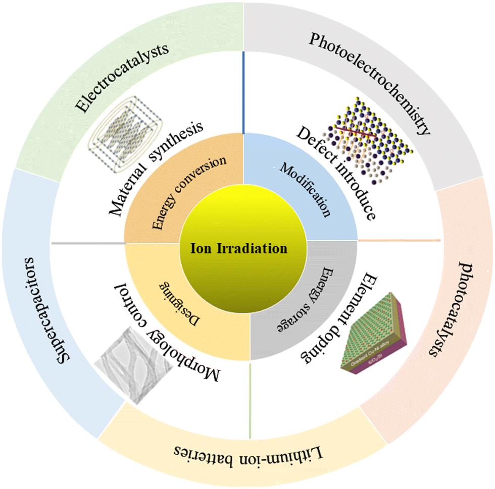 | ||
| Fig. 1 Design considerations of the application of the ion-irradiation technique for modifying and designing catalyst/electrode materials for energy storage and conversion devices. | ||
2. Fundamentals of the ion-irradiation technique
2.1 Concepts and principles of the ion-irradiation technique
Ion-irradiation is a technique that refers to ionizing the atoms of an element and then accelerating to a higher energy to make them possess a high kinetic energy. Then, they are injected into the surface of the target materials, resulting in a change in the physical or chemical properties of the material.The principles of ion-irradiation are shown in Fig. 2.17 First, the irradiated hot electrons from the ion source bombard the injected gas molecules for generating ions. Then, a magnetic analyzer is used to select specific elemental ions with mass–charge ratios. Subsequently, the ions are accelerated by a step through the accelerator to obtain a higher energy, and then focused through quadruple lenses to obtain uniform beam spots. Finally, the ion beam is uniformly injected into the surface of the solid sample using a deflection scanner. The ions with high energy will collide with the atoms and electrons of the solid target surface many times, thus weakening the energy of the implanted ions. Eventually, ions penetrate into the solid material to achieve the purpose of irradiation. During irradiation, a series of physical and chemical interactions can occur between the implanted ions and the solid sample.
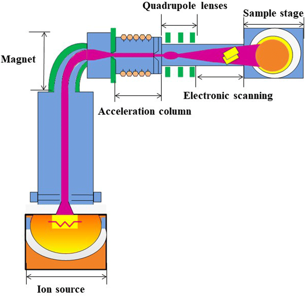 | ||
| Fig. 2 Basic structure of an ion implanter with magnetic analysis. Reproduced with permission from ref. 17, Copyright 2020, AIP Publishing. | ||
2.2 Composition of an ion implanter
The process of ion-irradiation on the sample is carried out using an ion implanter composed of an ion source, a magnetic analyzer, an accelerator, quadruple lenses, electronic scanning, and a target chamber (Fig. 3).18 The ion source is the main part of the ion-implantation implanter to produce ion beams with various strengths. Electrons produced by a direct current discharge or high-frequency discharge of an ion source act as the bombardment particles. When the energy of the foreign electron is higher than the ionization potential of the atom of targeted materials, the element is ionized by collision. A magnetic analyzer is used to select an elemental ion with a specific mass–charge ratio, and an accelerator is used to obtain higher energy of the ion-beam through a quadrupole lens.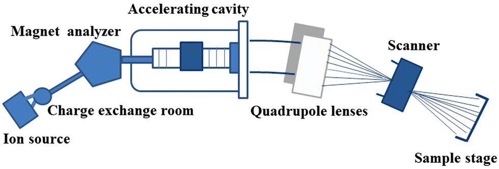 | ||
| Fig. 3 Schematic diagram of the ion-irradiation principle. Reproduced with permission from ref. 18. Copyright 2017, Wiley-VCH. | ||
2.3 Key parameters in the ion-irradiation process
For ion-irradiation, some irradiation parameters play a crucial role in modifying the properties of the targeted materials,19 including irradiated energy (E), ion fluence (NI), ion flux (j) and implantation temperature (T). The detailed explanations are as follows.2.4 Type of ion-irradiation and characteristics
Different irradiated energies correspond to various applications. The following types of ion-irradiation are often used for the modification of catalyst/electrode materials: low energy ion-irradiation, medium energy ion-irradiation, swift heavy ion-irradiation (SHII) and high charge ion-irradiation.The E of low energy ion-irradiation is usually less than 1 keV, which is widely used in materials as a common irradiation.20,21 Low-energy ion irradiation can modify the surface morphology and achieve the selective doping of two-dimensional materials. The ion-implantation with an energy up to tens of keV can effectively realize the defect engineering of two-dimensional materials.22,23
The E of medium energy ion-irradiation ranges from a few hundred keV to a few MeV and is suitable for the micro/nanostructure modification and elemental doping of various thin film electrode materials.17,19
The E of SHII is usually more than 1 MeV. At higher energy, inelastic collisions occur between incident ions and target electrons. For inelastic collisions, energy loss can be transformed into defects through indirect complex processes. Since the transferred energy is very large, a large number of defects can be generated at a very low flux.24 Therefore, a large number of defects can be produced at a very low fluence to engineer the defect structure and even the nano-morphology of the material.
High charge ion-irradiation is usually used in the modification of semiconductor materials. The high charge means that it possesses high potential energy, which is stored by removing many from the neutral atom. Potential energy is the sum of all binding energies of the lost electrons. It can reach ten to hundreds of keV.25,26 Highly charged ions are slower, and the target ion interactions are concentrated on the near-surface region.
Compared with other techniques, ion-irradiation possesses the following unique advantages:19
(1) Favorable controllability. In the irradiation process, there is a wide range of options and controllable implanted parameters (such as energy, fluency, and temperature). Therefore, ion-irradiation can precisely control the doping concentration and depth as well as longitudinal and transverse diffusion.
(2) High precision. Since the energy and fluence of implanted ions can be controlled, consequently, the depth and concentration of implanted ions in the host matrix can be accurately controlled during the implanted process.17
(3) High purity. Since the ion-irradiation is carried out in a vacuum system, it does not introduce other impurities. Meanwhile, a high resolution mass analyzer is used to ensure the high purity of the implanted ions.
(4) Favorable repeatability. Because the ion-irradiation technology is accurate, controllable, and accurately controls the parameters of the ion beam (species, energy, fluency, beam current, temperature, and so on),27 consequently, it has favorable repeatability.
(5) High flexibility. Since every type of ion-implantation has its unique characteristics, therefore, it can be selected to satisfy the different purposes of specific modifications of materials which include a variety of properties of thin films, solids and nanostructured samples.
3. Ion-irradiation effects on the catalyst/electrode materials
In this section, we will focus on the ion-irradiation/implantation effects on the catalyst/electrode materials, including the defect introduction, element doping, morphology control, and material synthesis, and these effects are helpful in material modification and design.3.1 Defect introduction
The electrochemical properties of the material are closely associated with defect structures. Introducing defects into materials is one of the promising approaches for improving the performance of materials. A great number of methods have been developed to introduce defects into materials, including plasma treatment,28 thermal annealing,29 chemical functionalization30 and ion irradiation.31 Among these methods, ion-irradiation can offer a wide range of controllability in the defect type by controlling the irradiation parameters such as the energy, type, and fluence of the injected ions.Sun et al.32 proposed using the C ion-irradiation to introduce sulfur vacancies to improve the hydrogen evolution reaction (HER) performance of MoS2. They found that the irradiation dose plays a major role in tuning the number of sulphur vacancies and the amorphous phase on the basal plane of MoS2 which improves the HER performance of MoS2. The superior activity for the HER is due to the vacancies generated by ion-irradiation, which exposes more active sites and thus improves the catalytic performance.
Also, He et al.33 fabricated a single-layer MoS2 and followed this by using 500 keV Au irradiation to generate sulfur defects (Fig. 4a). They further investigated the impacts of defects on the properties of MoS2. As the defect density increases, the characteristic photoluminescence (PL) peak of MoS2 was found to first shift to higher energy and then shift back to lower energy; after ion-irradiation, the electron transfers from MoS2 to the absorbed O2 at the defect sites, thus leading to a depletion of the electrons and an enrichment of the holes.
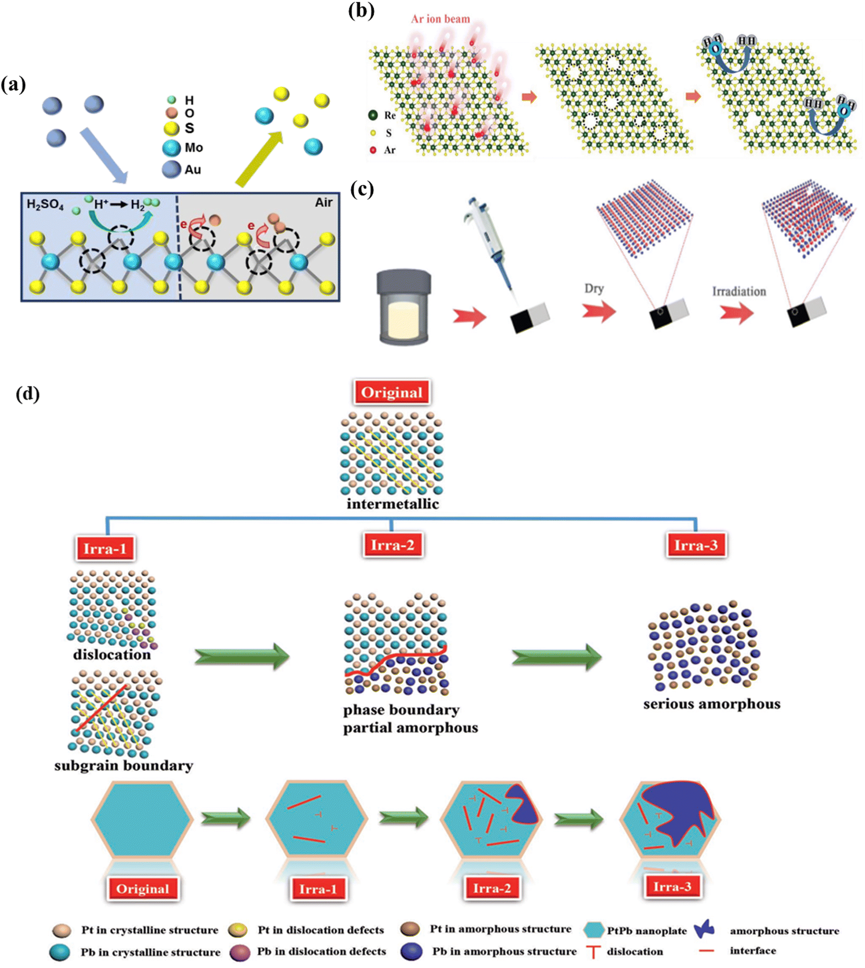 | ||
| Fig. 4 (a) Scheme illustration of the defects in MoS2 generated by Au ion-irradiation. Reproduced with permission from ref. 33. Copyright 2018, American Chemical Society. (b) Schematic diagram of Ar ion beam bombardment to 2D ReS2 nanosheets and the formation of atomic Re vacancy defects for enhancing catalysis toward the solar-driven PEC-HER. Reproduced with permission from ref. 34. Copyright 2018, Wiley-VCH. (c) Scheme illustration of the preparation procedure of Fe-Bi2Te3/Ti. Reproduced with permission from ref. 35. Copyright 2020, Royal Society of Chemistry. (d) Simulation models of PtPb nanoplate structure evolution by controlling the C+ ion fluences. Reproduced with permission from ref. 18. Copyright 2017, Wiley-VCH. | ||
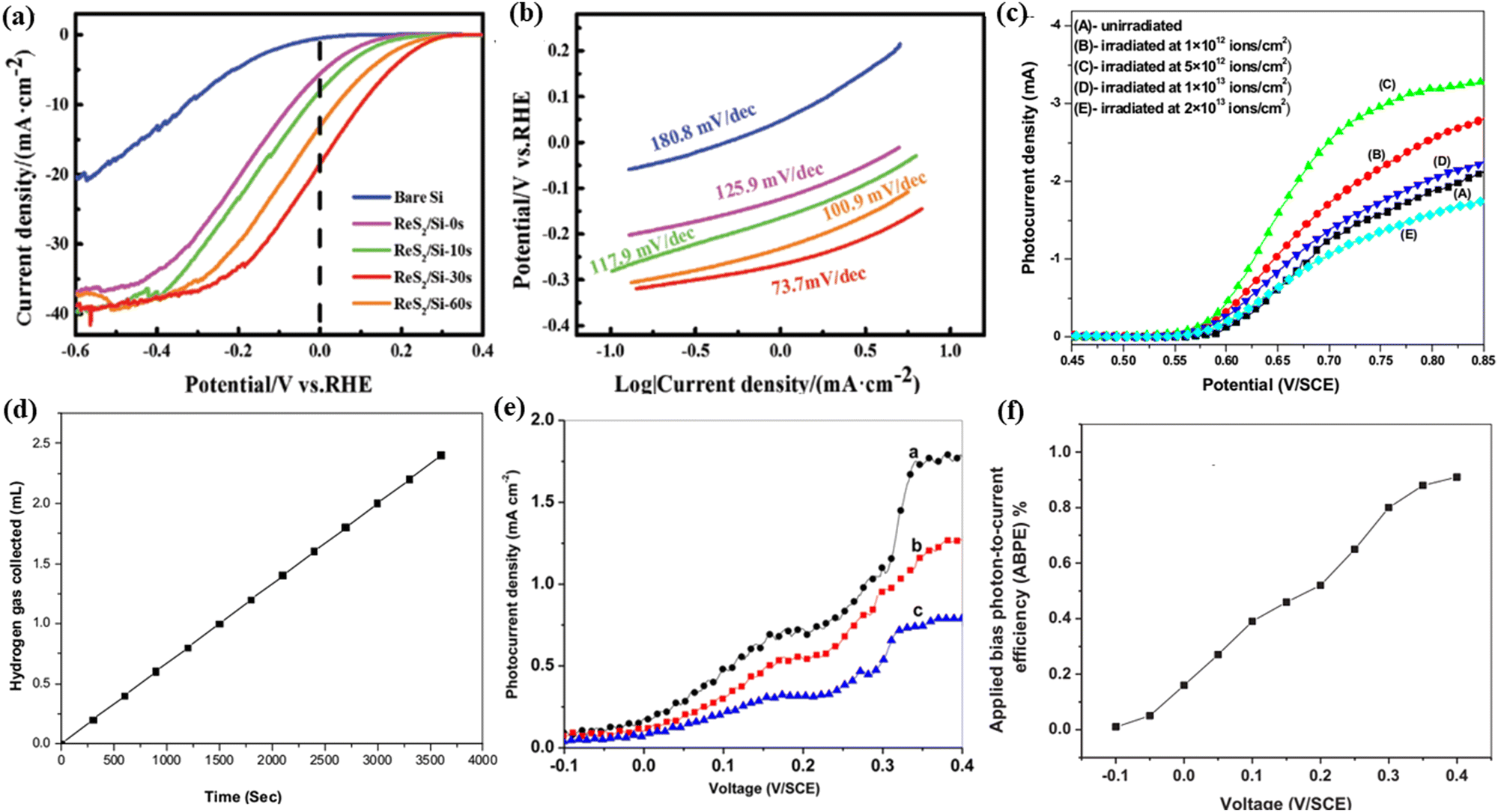
Huang et al.34 used a chemical vapor deposition (CVD) method to directly grow ReS2 nanosheets on a p-Si substrate, which was further irradiated with Ar ion-irradiation (Fig. 4b). Re defects were successfully introduced onto the ReS2/Si photocathode by ion-irradiation. The existence of Re vacancies not only produces adequate unsaturated S atoms but also influences intrinsic charge compensation from S to Re–Re bonds, allowing H+ to be absorbed on the active sites neither strongly nor weakly. In addition, the distinctive stacked 3D structure has the obvious benefit of exposing more active sites and larger superficial areas to contact with electrolytes. These two reasons jointly enhanced the solar-driven hydrogen evolution reaction (PEC-HER) performance of ReS2/Si photocathodes.
In a work by Wang,35 high-energy Fe ions (a dose of 4 × 10¹⁴ ions per cm2) were irradiated on the surface of Bi2Te3 nanosheets, which resulted in the generation of a variety of defects (Fig. 4c). The existence of defects resulted in an increase in the active sites and improvement in the conductivity of Bi2Te3, ensuring the rapid transfer and transport of charge during the catalytic process. Guo et al.18 reported a new strategy by controlling the defects of PtPb nanoplates using C+ ion-irradiation. By controlling the ion fluence, PtPb nanoplates could be well transformed from single crystal to polycrystal with various degrees of dislocations, subgrain boundaries, and partial amorphization. After ion-irradiation, PtPb nanoplates can largely maximize the Pt catalytic efficiency and utilization enhancing electrocatalytic performance (Fig. 4d). The same group36 synthesized PtPb NPs under nonaqueous conditions and followed this by 1 MeV Kr3+ ion-irradiation. Upon ion-irradiation, novel structure PtPd nanoplates are formed, in which the crystalline phase and amorphous phase co-existed; particularly, the crystalline phase is surrounded by the amorphous phase annularly to form a crystalline/amorphous interface. As a result, Kr3+ ion-irradiation makes the Pt electronic structure regulated due to the interface fusion of the crystalline/amorphous interface. Meanwhile, the crystalline/amorphous interface provides plenty of active sites, and the interface can activate the C–H and O–H bonds to enhance the catalytic performance.
Chen et al.37 prepared a single-layer MoS2 by the CVD method and transferred it onto various substrates such as Au, single-layer graphene (SLG), hexagonal boron nitride (BN) and CeO2, and created defects by Ar+ ion-irradiation (Fig. 5a). They explored the substrate effect on the electronic structure of MoS2 by a series of measurement. It was found that these substrates can tune the electronic energy levels in MoS2 due to the charge transfer that occurred on the interface. Furthermore, when the reduced CeO2 as a substrate upon annealing significantly affects the energy band alignment of MoS2 and CeO2/Au substrates, the reduction introduces electronic conductivity into the CeO2 substrate. The introduction of defects by ion-irradiation enhances the HER activity of single layer MoS2. The tunability of defect types and concentrations in MoS2 by ion-irradiation at different energies provides a possibility to engineer the properties of MoS2 and other two-dimensional (2D) materials.
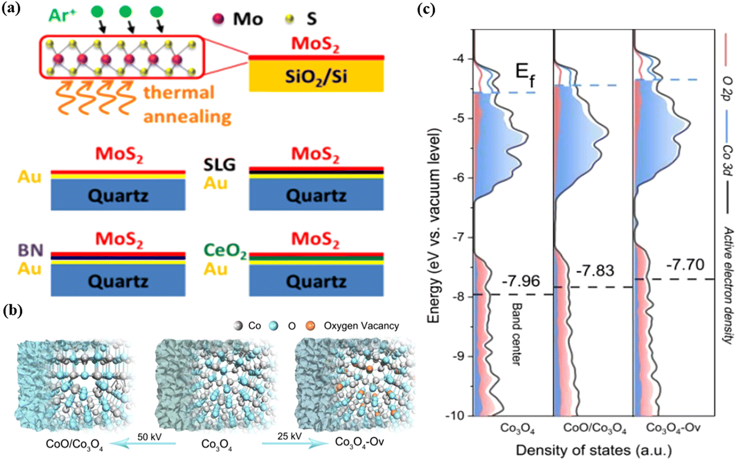 | ||
| Fig. 5 (a) MoS2/Au, MoS2/SLG/Au, MoS2/BN/Au and MoS2/CeO2/Au studied in the work. All the structures are supported by quartz substrates. The MoS2 single layers in all these structures are transferred from CVD grown MoS2 on the Si/SiO2 substrate. Vacuum thermal annealing or Ar+ irradiation is used to treat the samples to either enhance the contact with substrates or produce defects. Reproduced with permission from ref. 37. Copyright 2018, American Chemical Society. (b) Schematic illustration and (c) PDOS plots of Co3O4, Co3O4–Ov and CoO/Co3O4 samples. Reproduced with permission from ref. 38. Copyright 2020, Wiley-VCH. | ||
The introduced vacancies by ion-irradiation could also regulate the electron density of the material, which can help in better understanding of the relationship between the structure and performance. For example, He et al.38 fabricated a series of Co-based catalysts (oxygen defect -containing Co3O4 (Co3O4–Ov) and multi phased CoO/Co3O4) (a schematic illustration of Co3O4, Co3O4–Ov, and CoO/Co3O4 samples is shown in Fig. 5b) through Ar+ ion-radiation on pristine Co3O4. Co3O4 was subjected to argon ion-irradiation at 25 keV (Co3O4–Ov) and 50 keV (CoO/Co3O4) with a dosage of 5 × 10¹⁵ ions per cm2. The theoretical calculation and ultraviolet photoelectron spectrometer characterization together indicated that the band center of Co3O4 upshifted, thereby improving the adsorption capacity of the oxo group and greatly reducing the reaction barrier. This consequence further proved that the surface active electron density of Co3O4 can be effectively regulated by ion-irradiation (Fig. 5c).
3.2 Element doping
Ion-irradiation is known to be a novel and effective element doping means commonly used in metal oxides, heterojunctions, and graphene which usually involves two steps in fabricating materials including ion-implantation and annealing.Liu et al.39 successfully prepared noble metal nanoparticles and metallic (Fe, V) and non-metallic (N) doped TiO2 by ion implantation (the energy of 20–50 kV, with different ion sources Au, Fe, V, and N, at a fluence from 0.1 to 20 × 1016 ions per cm2) and subsequent annealing. After doping of Au, the photocatalytic activity of the Au–TiO2 sample was enhanced because of Au NPs in response to the incident light, which enhance the absorption, the local electric field and the excitation of active electrons and holes. For Fe doped TiO2, the hybridization of the Ti4+ 3d orbital with Fe3+ 3d orbitals occurs, which introduces a new energy in the band structure of TiO2 and therefore improves the response to visible light. For V-doped TiO2, the increased V doping promotes the transformation from the anatase to the rutile phase. Besides, the implanted V-doped TiO2 exhibits a red-shifted absorption edge which leads to a significant enhancement of light absorption in the visible light region. For N-doped TiO2, the experimental results and theoretical calculations demonstrate that the substitution of nitrogen for oxygen atoms in TiO2 induces an isolated localized state of N 2p above the O 2p dominant valence band. The TiO2-based composite films are fabricated by ion implantation (Au, Fe, V, and N element doping in TiO2) and show high crystallinity and stability, and the enhanced photocatalytic activities towards visible light were observed. The photocatalytic activity is greatly improved, suggesting that the N doping level had an obvious influence on the photocatalytic activity of the TiO2 samples. This report suggested that different irradiation sources can affect the properties of materials in different ways.
The same group reported the formation and thermal evolution of Al2O3 substrates by high fluence Zn+ ion implantation at different fluences (1 × 10¹⁷ and 2 × 10¹⁷ ions per cm2).40 They first implanted Zn+ onto the surface of the α-Al2O3 sample. Then, the implanted sample was annealed in an oxygen atmosphere at 700 °C for 2 h. During the annealing process, Zn+ diffused to the surface and was oxidized into ZnO which indicates that the implanted Zn+ was successfully doped onto the surface of α-Al2O3. Particularly, the higher quality ZnO film formed on the surface of Al2O3 single crystal at a fluence of 1 × 10¹⁷ ions per cm2 by Zn+ implantation combined with sequential annealing at 700 °C for 2 h in the oxygen atmosphere. Zhao et al.41 reported ion-implantation for the direct synthesis of nitrogen-doped graphene (NG). Firstly, they fabricated a newly multilayered substrate (Ni/Cu/a-SiC/SiO2/Si). Then, nitrogen ion-implantation (with an ion energy of 40 keV at 1 × 10¹⁶ ions per cm2) was performed on the multilayered substrate of Ni/Cu/a-SiC/SiO2/Si. Finally, the N ion-implanted substrate was annealed by using rapid thermal processing to obtain NG (Fig. 6a). Through nitrogen ion-implantation, they proved the successful synthesis of nitrogen-doped graphene using transmission electron microscopy (TEM), Raman spectroscopy, X-ray photoelectron spectroscopy (XPS), and the measurement of electronic properties, demonstrating that the N ion-implantation could effectively dope graphene. The ion-implantation technique not only can be expected to produce NG but also opens up a new way to extend more element doping of other materials.
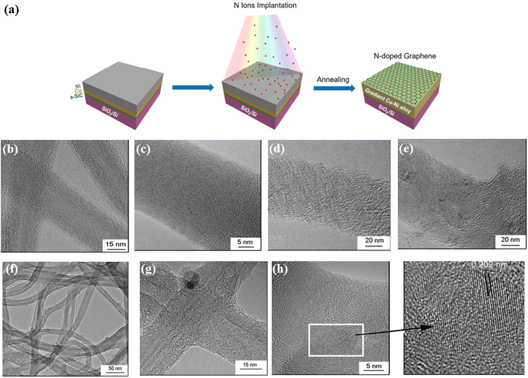 | ||
| Fig. 6 (a) Schematic illustration of the co-segregation method combined with ion implanation for one-step synthesis of NG. Transitions of MWCNTs to amorphous carbon nanowires under 70 keV N+ ion beam irradiation at room temperature. Reproduced with permission from ref. 41. Copyright 2018, Elsevier. (b) A MWCNT irradiated at a dose of 1 × 10¹⁶ ions per cm2 and (c) an MWCNT irradiated at a dose of 7 × 10¹⁶ ions per cm2. HR-TEM images of N+ ion irradiated defective MWCNTs (1000 K) at a dose of (d) 4 × 10¹⁶ ions per cm2 and (e) 7 × 10¹⁶ ions per cm2. (f and g) HR-TEM images of Ar+ ion-irradiated defective MWCNTs at a dose of 7 × 10¹⁶ ions per cm2 at 1000 K. (h) A diamond particle nucleates on a-CNWs under H+ ion beam irradiation at 1000 K, and the crystalline diamond structure with a spacing of about 0.202 nm was formed into a-CNWs at a dose of 1 × 10¹⁷ ions per cm2. Reproduced with permission from ref. 47. Copyright 2013, Elsevier. | ||
3.3 Morphology control
During the ion-irradiation process, the sputtering effect is a common phenomenon which is assumed to result from cascades of atomic collisions by energetic ions or recoil atoms.42–44 When energetic ions shoot into a target substrate, the incident ions impact the atoms of the target substrate, and these atoms may obtain enough energy to be ejected out of the substrate; thus, the surface sputtering effect can modulate the surface morphology of materials.45,46 Ishaq et al.47 used different ion fluences to investigate the effects of H+, N+, and Ar+ ion-irradiation on the structural and morphological changes of multi-walled carbon nanotubes (MWCNTs) and amorphous carbon nanowires (a-CNWs). They found that, at room temperature, defects were introduced in MWCNTs under 70 keV N+ ion beam irradiation at a low dose of 1 × 10¹⁶ ions per cm2. Meanwhile, under high fluence N+ irradiation (7 × 10¹⁶ ions per cm2), MWCNTs could transform into a-CNWs (Fig. 6b and c). At 1000 K, the 70 keV N+ ion beam irradiation of defective MWCNTs is transformed from curling of carbon clusters to an onion-like structure at a dose of 4 × 10¹⁶ ions per cm2 and the formation of an onion-like structure is at 7 × 10¹⁶ ions per cm2 (Fig. 6d and e). The type of the ion source also affects the morphology of MWCNTs. At 1000 K, under Ar+ ion-irradiation (7 × 10¹⁶ ions per cm2), the defective MWCNTs transform into a high-density onion-like structure (Fig. 6f and g). When the ion source is changed to an H+ ion source, the ion fluence is changed from 1 × 10¹⁶ to 1 × 10¹⁷ ions per cm2, and the a-CNWs gradually increase the fraction of the material with a diamond structure (Fig. 6h). These results showed that the change of ion-irradiation parameters (including ion irradiation energy, dose and annealing temperature) has been seen for crystalline–amorphous and amorphous–crystallization changes in the carbon nanostructure. Additionally, Jiang et al.48 utilized Ag ion-irradiation and annealing to fabricate hollow microsphere arrays. After Ag ion-irradiation, the surface of the polystyrene sphere (PS) microsphere was carbonized. Through annealing or chloroform immersion, the non-carbonated zone can be easily removed, and then the hollow microsphere. They have investigated the influence of the ion-irradiation energy and fluence on the morphology and structure of the PS microsphere array. They found that, at 15 kV, with the increase of Ag ion fluences (1 × 10¹⁶, 3 × 10¹⁶, and 5 × 10¹⁶ ions per cm2), the morphology and size of PS microspheres were almost unchanged. However, when the irradiated fluence reached 7 × 10¹⁶ ions per cm2, the coalescence phenomenon of neighboring PS microspheres occurred. Then, they chose this irradiated fluence (7 × 10¹⁶ ions per cm2) in subsequent experiments and attempted to change the energy to investigate the influence of ion-irradiated energy on the morphology of PS spheres. With the increasing irradiated energies (10, 15, 20, 40, and 60 kV), not only the morphology and size of the PS sphere but also the structure of the close-packed 2D hexagonal array has undergone dramatic changes. Under the same irradiated parameters, after thermal annealing at 350 °C for 30 min, the structure of samples has transformed into spherical shell arrays. The main reason for the formation of spherical shell arrays is due to the carbonization effect produced by calcination and the sputtering effect generated through ion-irradiation (regulating different irradiated parameters). The Ag ion beam modification diversifies the structure and morphology of the PS sphere array and greatly improves its thermostability.In a work by Giulian,49 Pt nanoparticles (NPs) in amorphous SiO2 were irradiated with 185 MeV Au ions in the fluences varying from 2 × 10¹⁴ to 2 × 10¹³ ions per cm2. From the TEM images, with the increasing irradiation fluence, it was observed that Pt NPs transform from spherical to rod-like shapes. The deformation process is studied as a function of the NP size, varying irradiation fluence and energy give a broad prospective of the shape transformation. Based on the above reports, the morphology of materials can be further regulated by changing ion-irradiation parameters (including ion irradiation energy, dose and annealing temperature), thus providing a broader application prospect for ion irradiation technology.
3.4 Material synthesis
Besides the modifications, as in an earlier study, ion-implantation has been used to synthesize nanoparticles. Taguchi et al.50 synthesized C-SiC coaxial nanotubes by ion-irradiation as shown in Fig. 7. Firstly, C-SiC coaxial nanotubes were synthesized by heat treatment of MWCNTs and Si powder without direct contact with each other at 1200 °C. Then, coaxial nanotubes were deposited on a molybdenum grid TEM sample holder with a holey-carbon layer. The deposited coaxial nanotubes were irradiated with both 200 keV Si ions with a dose of 1.1 × 10²¹ ions per cm2 and 400 keV electrons simultaneously using the TEM instrument. The hybrid consisted of one-dimensionally stacked graphene nanodisks with diameters less than 50 nm and cylindrical multiwalled carbon nanotubes inside an amorphous SiC tubular layer. A sudden emergence of new continuous graphitic layers in the microstructure was observed by in situ transmission electron microscopy following ion-irradiation, where these layers were perpendicular to the length direction of the nanotube. Also, Tsai et al.51 synthesized multilayer silicene by B ion-implantation. The boron ions were implanted into the target materials and reacted with carbon at the surface of SiC to form B4C during annealing. Simultaneously, silicon atoms were apparently squeezed out of the surface and then rearranged into the multilayer silicon.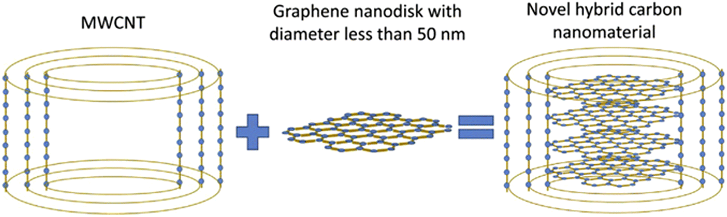 | ||
| Fig. 7 Schematics of the microstructure of novel hybrid carbon nanomaterials inside an amorphous silicon carbide nanotube synthesized by ion-irradiation. Reproduced with permission from ref. 50. Copyright 2019, Elsevier. | ||
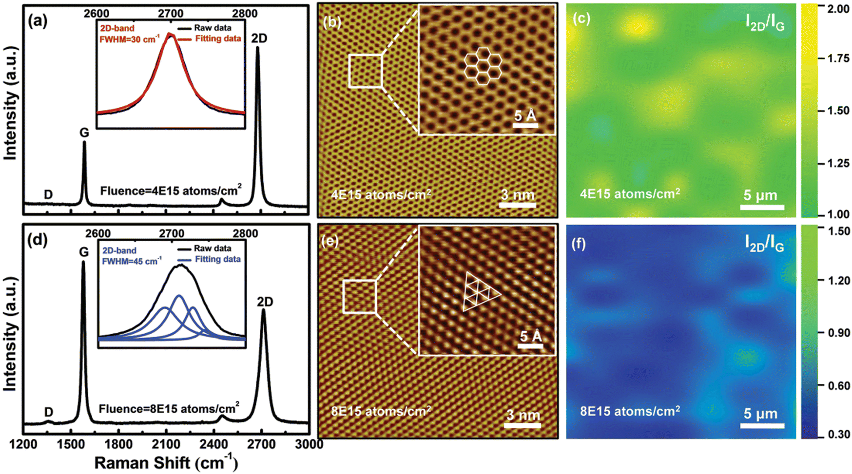
Zheng et al.52 fabricated tungsten oxide (WO3−x) nanowires by Ar+ ion beam irradiation and subsequently annealed them in a vacuum. In the first step, the WO3 thin film (∼70 nm thickness) was deposited on silica slides at 400 °C using an ultra high vacuum magnetron sputtering system. Then, the size of as-deposited WO3 thin films was controlled by tuning irradiation parameters (ion energies of 80, 130, 190 keV and with different fluences of 1 × 10¹⁷ and 1.5 × 10¹⁷ ions per cm2) and annealing conditions. The results demonstrated that the nanowire length increases with the increasing irradiation fluence and with the decreasing ion energy. The electrical conductivity of the nanowire film was higher than that of the pristine film, which is attributed to the high-density irradiation-induced vacancies on the oxygen sublattice greatly improving the conductivity. Furthermore, Wang et al.53 reported that the number of graphene layers can be controlled by modulating the C ion-implantation (with ion dosages of 4 × 10¹⁵ and 8 × 10¹⁵ ions per cm2). Fig. 8 shows the Raman spectra and scanning tunneling microscopy (STM) topographical images of the monolayer and bilayer graphene synthesized by ion-implantation. The Raman mapping result indicates that ion-implantation can fabricate highquality monolayer and bilayer graphene.
 | ||
| Fig. 8 Raman spectra of the (a) monolayer and (d) bilayer graphene. STM topographical images of the (b) monolayer and (e) bilayer graphene. The I2D/IG peak ratio derived from Raman mapping conducted on the (c) monolayer and (f) bilayer graphene. Reproduced with permission from ref. 53. Copyright 2015, Wiley-VCH. | ||
In general, this review involves the influence of ion-irradiation on materials, including defect introduction, element doping, morphology control and material synthesis. These effects are the means of modification/designing of catalyst and electrode materials, which is a positive effect. However, ion-irradiation is not suitable for the modification/designing of all materials. For example, the ultrathin nanosheet/nanoplate is easy to be penetrated.54–57 Consequently, materials may be unstable under ion-irradiation. In other words, ion-irradiation technology is not suitable for all catalyst/electrode materials.
4. Application of ion-irradiation technology in catalytic/electrode materials for energy conversion and storage
4.1 Application of ion-irradiation technology for electrocatalysts
Recently, the 2D MoS2 nanosheet as a promising alternative to Pt for the HER has drawn persistent interest. Several studies have revealed that the electrocatalytic HER performance of nanoscale MoS2 mainly arises from its edge states, while the basal plane is inert. If the inert basal plane sites can be optimized, meanwhile the edge activity can be maintained, the catalytic activity of MoS2 will be enormously improved.59–62 It was found that the inert basal plane of MoS2 could be activated by introducing sulphur defects into the surface. However, ion-irradiation is a novel strategy which can be used to introduce sulphur defects into MoS2 and thus improve catalytic activity.33,63,64 Sun et al.32 use C ions to irradiate MoS2 by regulating different C ion fluences (5 × 10¹², 2 × 10¹³, and 5 × 10¹³ ions per cm2). They found that ion-irradiation generates sulphur vacancies which were active sites on MoS2 basal planes, which could improve HER performance. It was shown that different ion fluences could tune the amount of sulphur vacancies and the amorphous region on the basal plane of MoS2. When MoS2 was ion-irradiated by a fluence of 2 × 10¹³ ions per cm2, the best HER performance could be achieved with an HER onset potential of 77 mV at 10 mA cm−2 and a small Tafel slope of 66 mV dec−1.
Different from the above low energy ion-irradiation, Madauss et al.65 used Xe ions (irradiated energy 91 MeV) to appropriately modify the MoS2 surface and thus achieved high catalytic activity for the hydrogen evolution reaction. At a potential of −0.6 V vs. RHE, the irradiated MoS2 exhibits a higher current density (35.3 mA cm−2) than non-irradiated MoS2 (−13.3 mA cm−2) (Fig. 9a). The irradiated sample has a smaller Tafel slope (104 mV dec−1) than the non-irradiated MoS2 (106 mV dec−1) (Fig. 9b). The results are due to a large increase in the number of low-coordinated Mo atoms after ion-irradiation, which can form bonds with adsorbing species and thus improving catalytic activity.
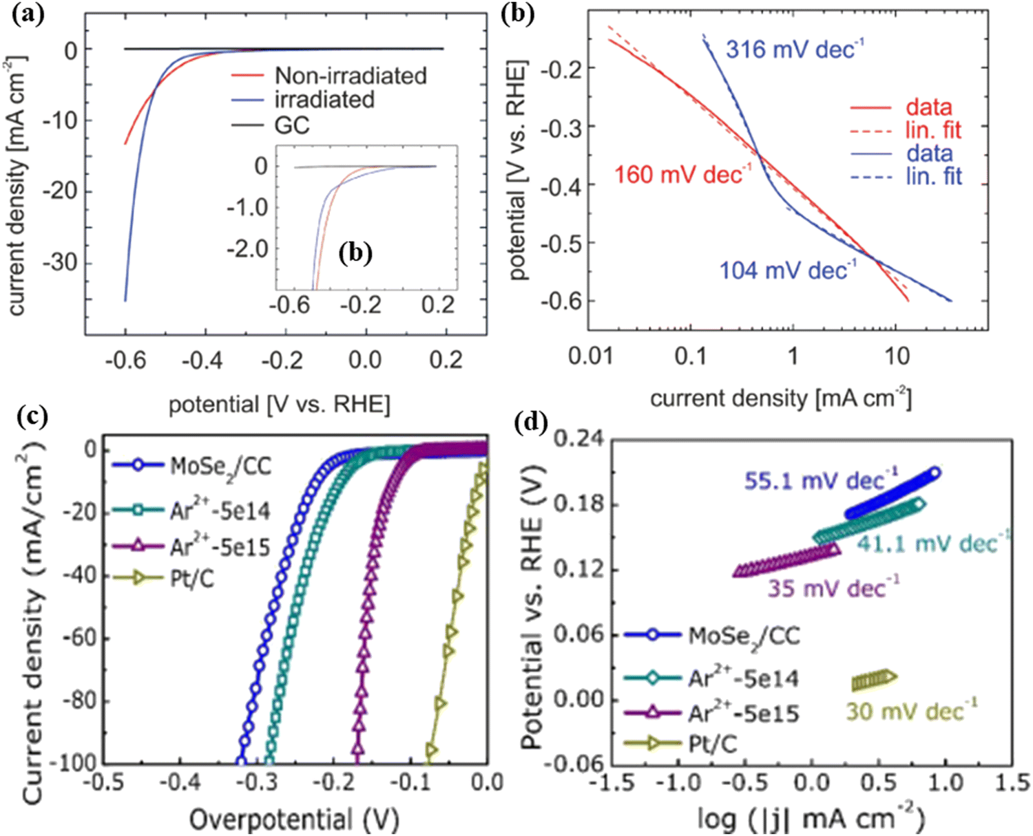 | ||
| Fig. 9 (a) Current density as a function of the potential (V vs. RHE) showing strong activity enhancement of the irradiated MoS2 compared to that of the non-irradiated MoS2. The inset of (a) shows the less negative onset potential for the irradiated MoS2. (b) V–I curves with Tafel-slopes of the irradiated (blue) and non-irradiated (red) MoS2. Reproduced with permission from ref. 65. Copyright 2018, Royal Society of Chemistry. The HER performance of the as-fabricated catalysts. (c) LSV curves and (d) Tafel plots of MoSe2/CC, Ar2+-5e14, Ar2+-5e15 and Pt/C electrodes, respectively. Reproduced with permission from ref. 66. Copyright 2018, American Chemical Society. | ||
Additionally, Xia et al.66 fabricated MoSe2 nanosheets grown on carbon cloth (CC) by the CVD method, which were subsequently irradiated by Ar2+ ions for providing additional active sites on the inert basal planes of nanosheets. MoSe2 was irradiated by using different doses of Ar2+ ions. Compared with pristine MoSe2/CC, the higher dose ion-irradiated MoSe2 nanosheets (5 × 10¹⁵ ions per cm2) showed the lowest overpotential of -171 mV (Fig. 9c) at a current density of −100 mA cm−2 and the smallest Tafel slope of 35 mV dec−1 (Fig. 9d). The first-principle calculation was employed to investigate the electron states of four different vacancy (single Mo vacancy (VMo), single Se vacancy (VSe), double Se vacancy (VSe2) and the absence of one MoSe2 molecular (VMoSe2)) cases observed in the MoSe2 basal plane. The calculated results showed that the pristine MoSe2 exhibits a higher bandgap (1.23 eV) than VMo and VSe2 band gaps (0.04 eV and 0.81 eV, respectively), which suggests the improved electronic conductivity, thereby promoting the electronic transferring during the HER process. Upon ion-irradiation, the existence of vacancies in the MoSe2 basal plane can not only lead to better conductivity but also produce more electrocatalytic active sites in MoSe2, ensuring the better HER catalytic ability of MoSe2.
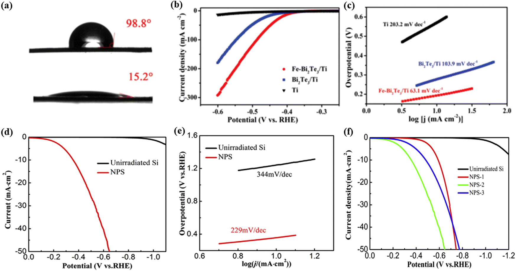
Wang et al.35 prepared Bi2Te3 nanosheets on a Ti plate and followed this by Fe+ irradiation, which can regulate the balance of hydrophilicity and hydrophobicity for the material. The contact angle result indicates that the Fe ion irradiated Bi2Te3/Ti exhibits hydrophilic properties, whereas the non-irradiated Bi2Te3/Ti exhibits hydrophobic properties (Fig. 10a). The result suggests that the Fe+ irradiation can manipulate the hydrophilicity/hydrophobicity balance of the Bi2Te3 surface, facilitating the release of hydrogen bubbles from the catalyst surface and exposing the active sites in time. While the damage caused by large bubbles on the electrode material was avoided, the stability of the material was improved (Fig. 10b and c). Silicon (Si) is rarely used as the HER catalyst due to its inert electrochemical activity. However, Wu et al.67 fabricated nanoporous Si as the HER catalyst by using Ar+ ion-irradiation followed by an annealing method. When the Ar+ ion-irradiation fluence reached 1 × 10¹⁷ ions per cm2, the nanoporous Si had more positive HER onset potentials and a smaller value of Tafel slope than the pristine Si (Fig. 10d and e). The higher catalytic HER activity of the irradiated Si could be attributed to the formation of nanopores during Ar+ irradiation, which promotes H2 bubbles escaping from the catalyst surface and thus exposes more active sites. They also investigated the influence of fluences (5 × 10¹⁶, 1 × 10¹⁷, and 2 × 10¹⁷ ions per cm2, respectively; the irradiated samples were named NPS-1, 2, and 3) on the HER performance of the samples. It was found that NPS-2 (at 1 × 10¹⁷ Ar+ ions per cm2 irradiated) showed the highest HER performance (Fig. 10f). The largely enhanced HER activity comes from the unique morphology and large specific surface area, which results from Ar+ ion irradiation and post-irradiation annealing. This method provides a novel research strategy to further improve the catalytic performance for energy conversion and catalysis.
 | ||
| Fig. 10 (a) Contact angles of Bi2Te3/Ti (top) and Fe-Bi2Te3/Ti (bottom), respectively. (b) LSV curves of the Ti plate, Bi2Te3/Ti, and Fe-Bi2Te3/Ti at a scan rate of 5 mV s−1. (c) The corresponding Tafel plots. Reproduced with permission from ref. 35. Copyright 2020, Royal Society of Chemistry. (d) Polarization curves of the nanoporous and non-irradiated Si. (e) Tafel slopes derived from the polarization curves. (f) The polarization curves for the fluences of NPS-1, NPS-2 and NPS-3. Reproduced with permission from ref. 67. Copyright 2018, Elsevier. | ||
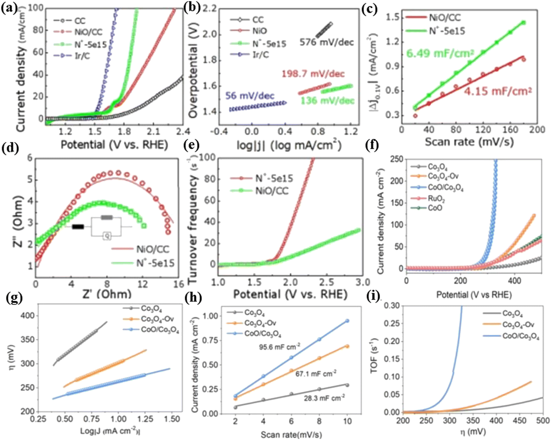
Xia et al.11 used N+ ion-irradiation (a dose of 5 × 10¹⁵ ions per cm2) to introduce N dopants and oxygen vacancies in NiO nanosheets grown on carbon cloth (Fig. 11a). In the experiment, N+ ion-irradiated NiO nanosheets exhibited a high OER performance with a potential of 1.98 V at a current density of 100 mA cm−2 (Fig. 11b). The double layer capacitance (Cdl) values of pristine and irradiated NiO/CC are estimated to be 4.15 and 6.49 mF cm−2, respectively (Fig. 11c), which demonstrate that the irradiated sample possesses larger effective electrochemical surfaces. The charge transfer resistance (Rct) value of the irradiated electrode is evaluated as 13.8 Ω, which is smaller than that of the pristine sample (16.9 Ω) (Fig. 11d), indicating the better electrical integration. The high turnover frequency (TOF) value (92.1 s−1) (Fig. 11e) demonstrates the high intrinsic activity of irradiated samples. Density functional theory (DFT) calculations further reveal that the introduced oxygen vacancies and opportune N dopants could narrow the NiO band gap which vested a better conductivity for charge transfer during the OER process. This work provides a novel path to enhance the OER electrocatalytic performance by ion irradiation.
 | ||
| Fig. 11 (a) LSV curves and (b) Tafel plots of carbon cloth, NiO/CC, N+-5e15 and Ir/C electrodes. (c) Capacitive measurement results. (d) Nyquist plots of NiO/CC and N+-5e15. (e) TOF of NiO/CC and N+-5e15. Reproduced with permission from ref. 11. Copyright 2019, Royal Society of Chemistry. (f) Polarization curves of the OER for Co3O4, Co3O4–Ov, CoO/Co3O4, CoO and RuO2. (g) Tafel plots of the OER for Co3O4, Co3O4–Ov and CoO/Co3O4. (h) Capacitive current measured at 1.16 V vs. RHE is plotted as a function of the scan rates of pristine Co3O4, Co3O4–Ov and CoO/Co3O4. (i) Potential-dependent TOF curves of Co3O4, CoO/Co3O4 and Co3O4–Ov. Reproduced with permission from ref. 38. Copyright 2020, Wiley-VCH. | ||
He et al.38 reported a novel strategy using an Ar+ ion-irradiation technology to regulate the electronic properties of Co-based catalysts (including oxygen vacancy-containing Co3O4 (Co3O4–Ov) and multi phased CoO/Co3O4) as OER catalysts. Co3O4 was subjected to argon ion-irradiation at 25 keV (Co3O4–Ov) and 50 keV (CoO/Co3O4) with a dosage of 5 × 10¹⁵ ions per cm2. Notably, CoO/Co3O4 demonstrates a much higher current density and lower onset potential than Co3O4–Ov (Fig. 11f). The overpotential of CoO/Co3O4 (270 mV) is lower than that of the pristine Co3O4 (410 mV) at 10 mA cm−2. The Tafel slope of CoO/Co3O4 (55 mV dec−1) is smaller than those of the pristine Co3O4 (169 mV dec−1) and Co3O4–Ov (92 mV dec−1), indicating the favorable OER kinetics for the multi-phased CoO/Co3O4 sample (Fig. 11g). In addition, the Cdl of CoO/Co3O4 is 95.6 mF cm−2, which is higher than that of other samples (Fig. 11h). These results indicated that more active sites were generated and exposed to the irradiation of Ar+ ions. Besides, the calculated TOF value of CoO/Co3O4 (Fig. 11i) is higher than those of Co3O4–Ov and CoO, suggesting its high intrinsic activity. Introducing Ar+ ion radiation can effectively modulate the surface active electron density of Co3O4 by forming the CoO phase and oxygen vacancies, which can precisely and appropriately enhance the adsorption capacity of the oxo group and greatly reduce the reaction barrier. Using the ion-irradiation technology has great potential to be developed as a general strategy to regulate the surface electronic properties of metal oxides.
4.2 Application of the ion-irradiation technique for photoelectrochemistry
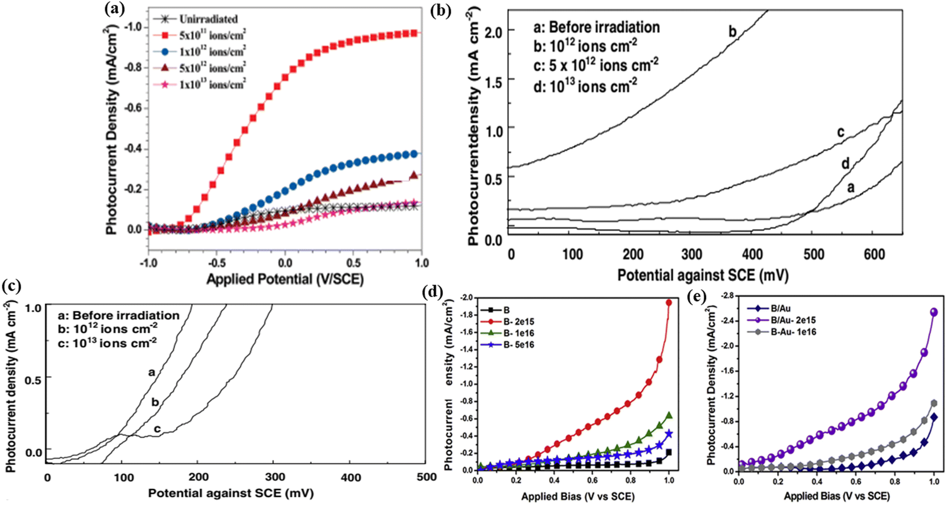
Photoelectrochemical (PEC) water splitting has been considered to be a promising clean technique for generating hydrogen gas,84 which has attracted much attention due to the increased demand for renewable energy.85,86 Semiconductors are eminently attractive electrode materials for solar-driven PEC water splitting.34,87,88 To better improve photo-redox reactions, these semiconductors must have a rational bandgap for being activated (i.e., photoexcitation) by light absorption.89,90 Many types of semiconductors such as TiO2, α-Fe2O3, and BiVO4, etc. have been intensively researched as potential photoelectrodes.91–95 Ion-irradiation has been playing an important role in modifying the properties of semiconductor materials. In general, the ion-irradiation effects on semiconductor materials are manifested as the changes in optical, physical, and electrical properties.Singh et al.96 reported the effect of 120 MeV Ag9+ ion-irradiation on the PEC properties of TiO2 thin films deposited on a conducting glass substrate (SnO2:In). The PEC properties of the films were found to be greatly affected by the fluence of irradiation. The optimal observed fluence of radiation for the best PEC response was 5 × 10¹¹ ion per cm2, at which the photocurrent density reaches a maximum of 0.76 mA cm−2 (Fig. 12a). The irradiated samples also exhibited a maximum flat-band potential at the junction and a maximum charge carrier density. The satisfying PEC properties by ion-irradiation may be due to the formation of the desired structure of vertically aligned grains caused by ion-irradiation, which can efficiently separate the photogenerated electron–hole pairs before recombination. Dass et al.97 modified the nanostructured 2%Cr–Fe2O3 and CuO thin films by using Au13+ SHII for PEC. The photocatalytic activity of the 2%Cr–Fe2O3 thin film irradiated increases at a fluence of 1012 ions per cm2, which might be due to more efficient absorption of photons resulting from the introduction of defects and the occurrence of structural rearrangements. Furthermore, it was observed that the decrease in photoresponse of irradiated 2%Cr–Fe2O3 and irradiated CuO thin films at higher fluences of 1013 and 1012 ions per cm2 (Fig. 12b and c) is attributed to the formation of a large number of discontinuities or dislocations in films. These defects act as recombination centers for photogenerated charge carriers, resulting in the decrease of the photocurrent.
 | ||
| Fig. 12 (a) Photocurrent density curves of non-irradiated and 120 MeV Ag9+ ion irradiated TiO2 thin films at different fluences. Reproduced with permission from ref. 96. Copyright 2010, American Chemical Society. (b) Observed photocurrent density as a function of applied potential with 2% Cr doped Fe2O3 thin film electrodes before and after SHI irradiation. (c) Observed photocurrent density as a function of applied potential with CuO thin film electrodes before and after SHI irradiation. Reproduced with permission from ref. 97. Copyright 2006, Elsevier. (d) and (e) Photocurrent density vs. applied bias for BiVO4 and BiVO4/Au photoanodes. Reproduced with permission from ref. 88. Copyright 2019, Elsevier. | ||
Srivastav et al.88 investigated the effect of N+ ion-irradiation on plasmonic Au nanoparticle loaded BiVO4 photoelectrodes for PEC water splitting. At an irradiated 2 × 10¹⁵ ions per cm2 fluence, the BiVO4/Au photoanode shows a photocurrent density of 2.54 mA cm−2 (an increase of approximately 92% in the photocurrent density) higher than the pristine BiVO4. Besides, the onset potential for BiVO4/Au is close to 0.1 V/SCE (Fig. 12d and e). The result is due to the improvement in the photon harvesting rate, reduced charge carrier recombination rate, and better separation of charge carriers, after irradiation. Meanwhile, the formation of Au nanoparticles favors the PEC water splitting by optical enhancement and photon scattering.
In a work by Huang,34 atomic vacancies are introduced onto two-dimensional ReS2 on Si by using controllable Ar ion-irradiation. The irradiated ReS2/Si photocathode demonstrated a highly enhanced catalytic activity for PEC water splitting. A high photocurrent density of −18.5 mA cm−2 at 0 V versus RHE was achieved in 30 seconds for the irradiated ReS2/Si photocathode (Fig. 13a), which is higher than that for non-irradiated ReS2/Si. Additionally, the Tafel plot shows that the photocathode of ReS2/Si-30s possesses the lowest Tafel slope of 73.7 mV dec−1 (Fig. 13b). The enhanced HER performance is mainly attributed to the rich and controllable atomic Re vacancies on the ReS2 nanosheets by ion-irradiation. Also, the impedance spectroscopy measurements indicated that the photocathode of ReS2/Si-30s had a relatively small Rct at the semiconductor/electrolyte interface, reflecting the fastest electrode-to-electrolyte shuttling of electrons during the HER.
 | ||
| Fig. 13 PEC activity measurements of different photocathodes under 100 mW cm−2 light energy. (a) LSV curves and (b) Tafel plots. Reproduced with permission from ref. 34. Copyright 2018, Wiley-VCH. The PEC performance of the hematite electrode: (c) Photocurrent density versus applied potential curves before and after ion-irradiation and (d) volume of hydrogen generated versus time at 0.75 V/SCE for the sample irradiated at 5 × 10¹² ions per cm2. Reproduced with permission from ref. 98. Copyright 2012, Elsevier. (e) I–V curve giving photocurrent densities of BaTiO3 films irradiated at (a) 1 × 10¹¹, (b) 2 × 10¹¹ and (c) 3 × 10¹² ions per cm2. (f) Variation of the applied bias photon-to-current efficiency with an applied voltage for the film irradiated at 1 × 10¹¹ ions per cm2. Reproduced with permission from ref. 99. Copyright 2013, Elsevier. | ||
Kumar et al.98 synthesized thin films of hematite (α-Fe2O3) by electrodeposition and after 100 MeV Si8+ SHII, the irradiated film exhibited a significantly improved PEC response than the non-irradiated α-Fe2O3 sample. The irradiated film at a fluence of 5 × 10¹² ions per cm2 exhibited the highest photocurrent density of 3.0 mA cm−2 and a hydrogen production rate of 2.4 mL h−1 cm−2 (Fig. 13c and d). The explanation might be that the irradiation could induce a decrease in the resistivity, an increase in the donor density and an increase in the flat-band potential for the sample, which may be responsible for its enhanced PEC properties.
The sample group also found that the BaTiO3 film was a potential candidate photoelectrode for PEC water splitting due to its extraordinary stability in aqueous environments.99 The fabricated BaTiO3 thin films are irradiated by 120 MeV Ag9+ irradiation at four different fluences (1 × 10¹¹, 2 × 10¹¹, and 3 × 10¹² ions per cm2). At a fluence of 1 × 10¹¹ ions per cm2, the BaTiO3 film achieved a maximum photocurrent density of 1.78 mA cm−2 at 0.4 V vs. SCE (Fig. 13e), which is ten times larger than that of the pristine sample, and the maximum conversion efficiency of 0.91% was exhibited by the same photoelectrode which is about 30 times larger than that of the pristine sample (Fig. 13f). The better PEC performance by ion-irradiation is attributed to improved optical absorption capability, increased roughness, efficient separation of charge carriers, and maximum flat-band potential and donor density.
Zheng et al.91 synthesized TiO2 nanorods by the atomic layer deposition (ALD) method followed by different energies (45, 65 and 85 keV) of N+ ion-irradiation. They studied the influences of the irradiated ion energy on the morphology and photocurrent density of the nanorods. And it was found that the length of nanorods increases with the increasing ion energy while the photocurrent does not increase continually with the increasing ion energy due to the heavier damage formed in TiO2 irradiated by N+ ions with higher energy. The nanorod array photoelectrode displays largely enhanced performance for PEC water splitting compared to that of the non-irradiated TiO2 thin films; this optimized PEC performance is attributed to the effects of N+ ion-irradiation, and the nanorod thin films have the larger TiO2/electrolyte interfacial area, which facilitates the hole transfer kinetics at the TiO2/electrolyte interface. This work proposes that ion-irradiation could be an effective approach for developing nanostructured materials for water splitting.
Normally, the PEC water splitting reaction process consists of another necessary reaction of the OER (2H2O + 4H+ → O2 + 4H+), which is also known to be the restricting step for the overall reaction. In a work by Zhan,100 the surface of TiO2(110) at different setting heating plate temperatures (300 °C, 400 °C, and 500 °C) and the relationship between the geometric, electronic structure and the PEC activity were investigated by using low-energy Ar+ irradiation. The irradiated TiO2 photoanodes showed much enhanced photoresponse with T-500 (setting heating plate temperature 500 °C) showing the highest activity. After 6 h, the photocurrent density of the T-500 photoanode is barely changing, which indicated the high stability of T-500. These optimal results are due to two reasons: one reason is that controlled formations of the oxygen vacancy, Ti3+, Ti2+, and Ti metallic species were achieved at the surface of TiO2, rendering a significant improvement in its light absorption, and charge carrier concentration, and charge transfer properties after Ar+ irradiation. And the second reason is that Ar+ irradiation can change the interaction between the TiO2 surface and water interface, making it more propitious to water decomposition. Thus, low-energy Ar+ irradiation could significantly improve the PEC performance of the TiO2 photoanode.
4.3 Application of the ion-irradiation technique for photocatalysts
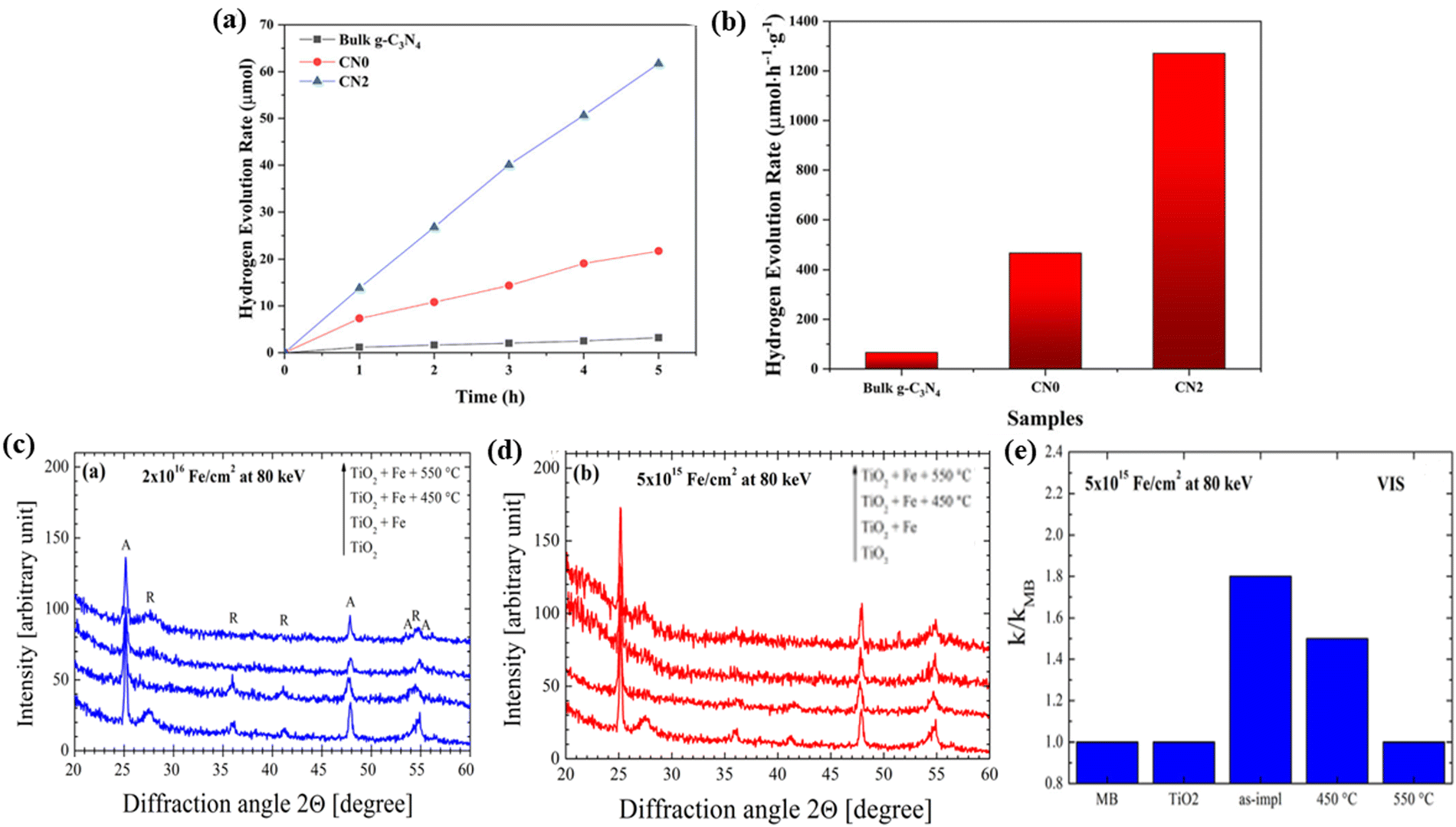
Photocatalysis is one of the most important topics in chemical research and has attracted tremendous interest in recent years owing to the need for renewable and sustainable energy.101–103 The most used photocatalysts are semiconductors, whose performance is substantially limited by the lack of visible-light absorption and poor photo-generated charge carrier separation efficiency. Defect engineering, as an effective strategy, can introduce vacancies that improve visible light absorption and charge carrier separation efficiency.104–107 The ion-irradiation technique is a novel method to introduce vacancies; due to the cascade collision of irradiation ions with target atoms, vacancies will be introduced into target materials. Importantly, the concentration and distribution of the incident vacancy are controlled by ion fluence and energy.Ren et al.108 used He+ ion-irradiation to efficiently introduce both defined C- and N-vacancies (VC and VN) in graphitic carbon nitride (g-C3N4) for photocatalytic water splitting. The existence of VN introduces the defect state in the band gap, which could improve the visible light absorption and increase the charge carrier separation efficiency thus resulting in the enhanced photocatalytic performance of g-C3N4. The photocatalytic performances of CN0 (pristine g-C3N4 nanosheet film) and CN2 (He+ ions fluence of 1.725 × 10¹⁴ ions per cm2) were evaluated by the photocatalytic hydrogen evolution test (Fig. 14a and b). As shown in Fig. 14b, the CN2 sample with an optimized vacancy concentration showed that a superior hydrogen evolution rate reaches 1271 mmol g−1 h−1 which is 2.7 and 19 times higher than the CN0 nanosheets and bulk g-C3N4, respectively. This work proved that the ion-irradiation technique is an effective approach for improving the photocatalytic performance of materials.
 | ||
| Fig. 14 (a) Hydrogen evolution curves. (b) Photocatalytic hydrogen evolution rates over the bulk g-C3N4, CN0, and CN2 samples under visible light irradiation. Reproduced with permission from ref. 108. Copyright 2019, Wiley-VCH. XRD patterns of the pure TiO2 film, as-implanted and after the thermal treatment of the Fe+ fluence of 2 × 1016 cm−2 (c) or 5 × 1015 cm−2 (d) at 80 keV. Photocatalytic rate of MB, normalized to the value obtained for MB in the absence of the photocatalyst, for different Fe+ implanted films: (e) 5 × 1015 cm−2 under UV light irradiation. Reproduced with permission from ref. 102. Copyright 2014, AIP Publishing. | ||
Besides metal-free g-C3N4, Impellizzeri et al.102 showed the application of Fe+ ion-implantation to realize an efficient TiO2 photocatalyst. The increase of the Fe+ irradiation fluence could enhance the damage of TiO2, which could cause strong electron–hole recombination, thus affecting the photocatalytic activity of the as-implanted film. They found that the peak intensity in the X-ray diffraction (XRD) pattern reduces gradually with the increase of the ion-irradiation fluence. The observed reduction in the peak intensity can be related to a damaging process attributed to the ion-implantation process (Fig. 14c and d). Under the fluence of 5 × 10¹⁵ ions per cm2, the as-implanted film revealed a remarkable photocatalytic efficiency in the degradation of organic compounds in water under visible light irradiation (80% higher than the one obtained for pure TiO2 films) (Fig. 14e), without the help of any thermal treatments. They further proved that the photocatalytic activity in the degradation of organic compounds strongly depends on the number of defects induced by the ion-implantation process.
The heterojunction semiconductor is also an important sort of material in photocatalysis. In a work by Wang,109 ZnO NWs were coupled with a narrow bandgap semiconductor material CdTe through a series of aqueous chemical reactions and were further irradiated with different doses of N ions to enhance the photocatalytic activity. They investigated the intensity of PL peaks at various cycles of CdTe/ZnO heterostructures, and it was found that the ZnO–CdTe-20-cycle heterostructures exhibit a lower PL peak intensity than that of other cycles ZnO–CdTe, which indicates the lowest recombination rate of photo-generated carriers. Additionally, in all samples of CdTe/ZnO heterostructures, ZnO–CdTe-20-cycle samples perform the highest photocatalytic activity. The CdTe/ZnO heterojunction nanostructures efficiently enhanced their photocatalytic performance mainly through the introduction of oxygen vacancies by N ion-irradiation, which can narrow the bandgap to improve the visible absorption ability and effectively separate electrons and holes.110–112
4.4 Application of the ion-irradiation technique for lithium-ion batteries
Lithium-ion batteries are regarded as efficient energy storage devices, which have been widely used in every corner of life, such as smart-phones, laptops, and electric vehicles because of their high specific energy and energy densities as well as their long cycling life. Ion-irradiation has appeared as an effective technique for introducing defects into materials to improve performance. Using the ion-irradiation technology to control the evolution of defects in electrodes is an effective method to improve battery performance.113Germanium (Ge) as an anode material has drawn a great deal of interest due to its high specific capacity (1623 mA h g−1) and Li+ diffusivity.114,115 Under high doses of ion-irradiation, the Ge morphology transformed from a nonporous structure to a nanoscale porosity interdigitated network.116–118 When used as an anode, the network could help in relaxing stress during the cycling process. Rudawski et al.119 fabricated ion-beam modified Ge films for lithium-ion batteries. Compared with the as-deposited Ge film, the ion beam-modified Ge nanostructured electrodes exhibited a specific charge (discharge) capacity of ∼1279 (∼1259) mA h g−1 with a coulombic efficiency of 98.4% for the first cycle. After 25 cycles, the specific capacity slightly decreases to 1352 mA h g−1 which is much higher than that of the deposited film (∼200 mA h g−1) (Fig. 15a). When the cycling rate increased to C/0.9, the specific capacities were still greater than 1000 mA h g−1 (Fig. 15b). The result suggests that the ion beam-modified Ge nanostructured electrode has great promise for use in high performance Li ion batteries.
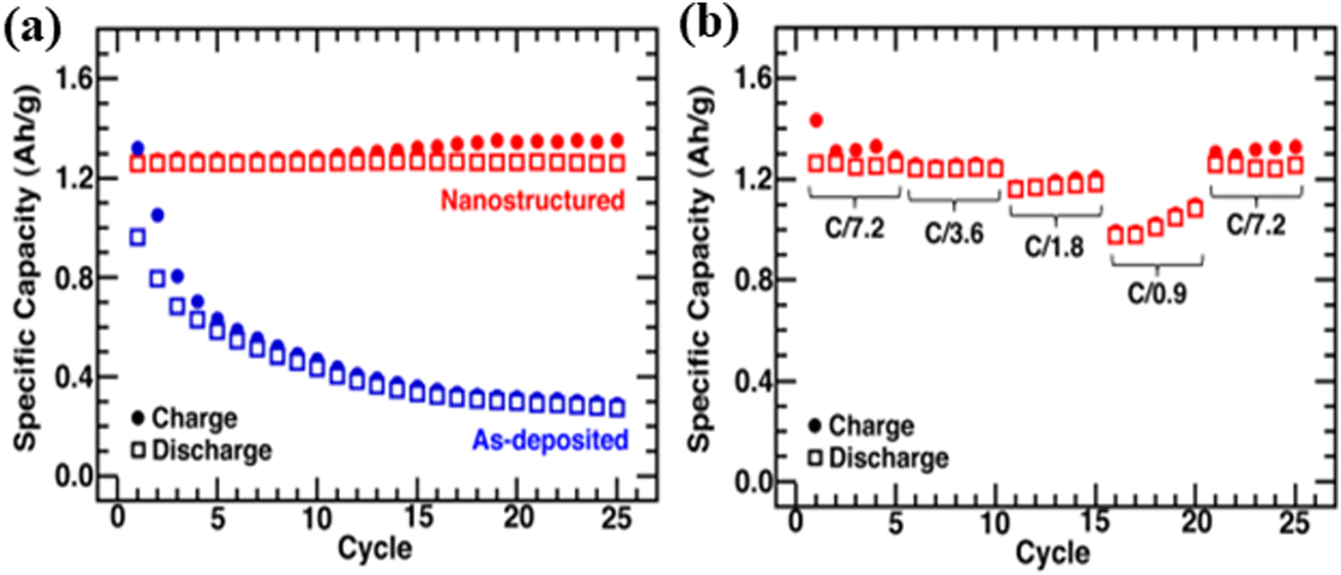 | ||
| Fig. 15 (a) Specific capacity versus cycle number for a nanostructured Ge electrode cycled at a C/7.2 rate for 25 cycles; the data of the as-deposited Ge electrode cycled at the same rate is provided for comparison. (b) Specific capacity versus cycle number for the nanostructured Ge electrode cycled sequentially at C/7.2, C/3.6, C/1.8, C/0.9, and C/7.2 rates, respectively. Reproduced with permission from ref. 119. Copyright 2012, AIP Publishing. | ||
Different from the above mentioned, Rahman et al.120 first utilized in situ high-energy Kr ion-irradiation combined with transmission electron microscopy to monitor how the defects and microstructures evolve in Na and Li-layered cathodes. The phase pure crystal structure along with the electrochemical performance shows that Na2/3Fe1/2Mn1/2O2 and LiNiO2 are representative and can provide a valuable guideline for designing stable layered cathodes under extreme conditions, such as outer space exploration and nuclear power industries. The quantitative mathematical analysis of the dynamic bright-field imaging shows that defect clusters preferentially align along the Na/Li ion diffusion channels (a–b planes), which is likely governed by the formation of dislocation loops. This study provides a valuable guideline for designing stable layered cathodes under extreme conditions, such as outer space exploration and nuclear power industries.
4.5 Application of the ion-irradiation technique for supercapacitors
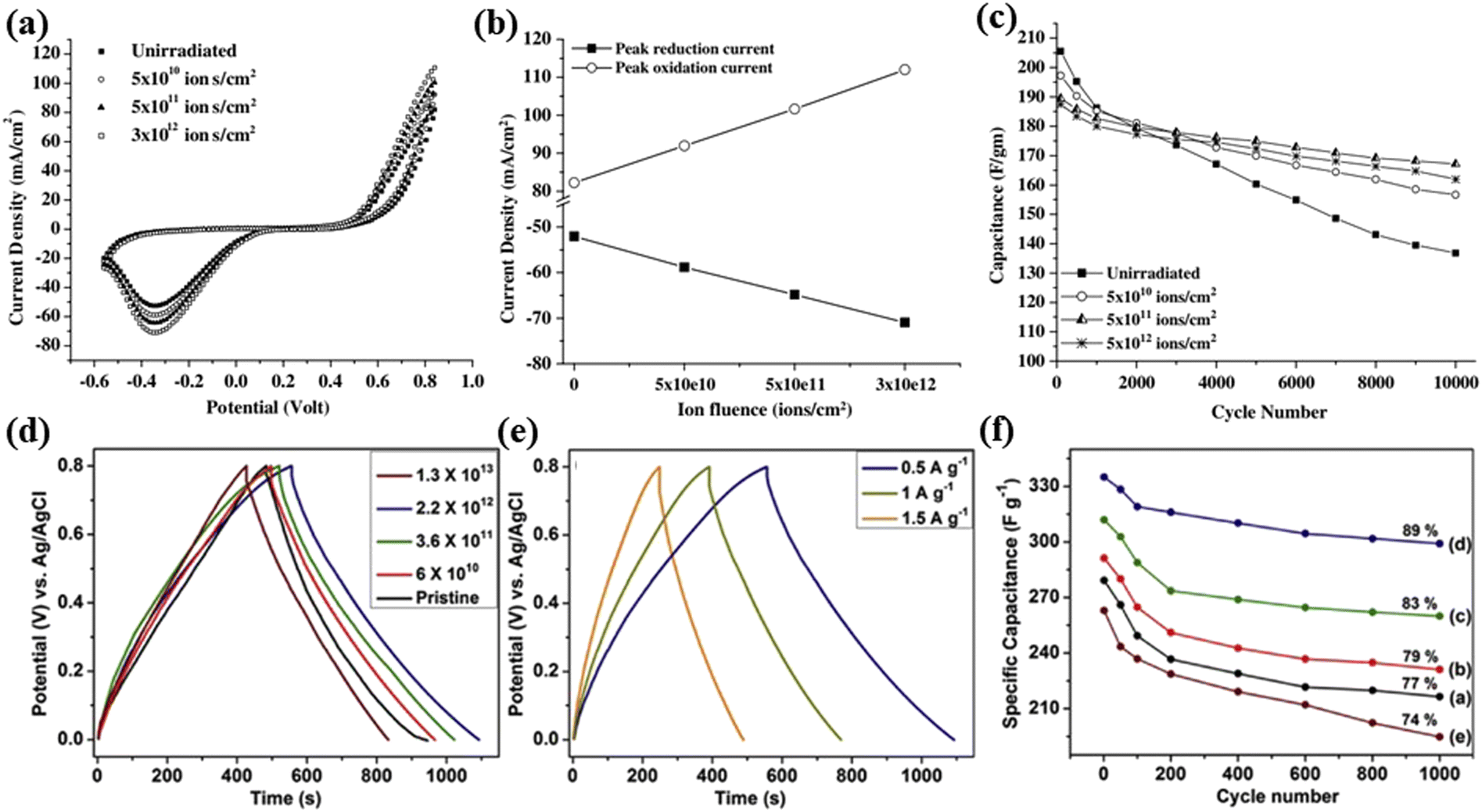
Besides batteries, supercapacitors can also serve as energy storage devices, which usually include electrical double layer capacitors (EDLCs) and pseudo-capacitors (PC). Compared with batteries, supercapacitors can provide higher power density and long cycling life. However, the restriction of charge storage on the electrode surface makes their capacity much lower than batteries.121–123 Among different electrode materials, electroactive polymers generally show a higher specific capacitance due to their ability to store charges by faradaic reactions on the surface.124 Interestingly, the ion-irradiation technique has been proved to be effective in improving the electrical conductivity and generating active sites for the surface physical and chemical modification of the polymers.125 The irradiated polymers could form new chemical bonds, intermolecular crosslinking, chain scissoring or fragmentation of molecules, bond-breaking, and formation of unsaturated groups by ion-irradiation, thus improving the performance of supercapacitors.126Hussain et al.127 electrochemically synthesized LiClO4 doped polypyrrole thin films on an indium tin oxide coated glass substrate, which was subsequently ion-irradiated by 160 MeV Ni12+ ions at different fluences of 5 × 10¹⁰, 5 × 10¹¹, and 3 × 10¹² ions per cm2. The irradiated polymer films demonstrated an increase in the magnitude of oxidation and reduction peak current (Fig. 16a), which is mainly due to the increase in the conductivity of the polymer films. Then, the conductivity of the polymer films was investigated, and the results indicated that the conductivity of the films shows an increasing trend with an increase in the ion fluence. The irradiated film exhibits a higher conductivity (150–160 S cm−1) than the pristine film (100 S cm−1), which is attributed to bond breaking that occurs due to cross-linking and chain scission which creates a large number of free electrons and thus increases in the conductivity of the polymer films. A plot of the oxidation peak current and reduction peak current (Fig. 16b and c) shows that the peak current of oxidation and reduction increases linearly with an increase in the fluence. In addition, the irradiated (fluence 5 × 10¹¹ ions per cm2) polymer film exhibits a higher capacitance than non-irradiated films after 10![[thin space (1/6-em)]](https://www.rsc.org/images/entities/char_2009.gif) 000 cycles.
000 cycles.
 | ||
| Fig. 16 (a) Cyclic voltammograms of polypyrrole films doped with LiClO4 before and after ion-irradiation at a potential 50 mV s−1 scan rate. (b) Peak oxidation and reduction currents versus ion fluence. (c) Stability plots of supercapacitors with LiClO4 doped polypyrrole electrodes. Reproduced with permission from ref. 127. Copyright 2005, Elsevier. (d) GCD curves of the pristine and ion-irradiated RGO-PPyNT nanocomposites with different fluences. (e) GCD curves of RGO-PPyNT nanocomposites irradiated at a fluence of 2.2 × 10¹² ions per cm2 at different current densities. (f) Variation of the specific capacitance with cycle number of RGO-PPyNT nanocomposites. Reproduced with permission from ref. 121. Copyright 2018, Elsevier. | ||
Devi et al.121 synthesized hybrid nanocomposites of reduced graphene oxide (RGO) and polypyrrole nanotubes (PPyNTs). The electrical properties of RGO-PPyNTs have been impacted by SHII with 85 MeV C6+ ions at different fluences. The galvanostatic charge–discharge measurements (Fig. 16d and e) show a nearly linear and symmetric discharge–charge curve indicating a typical EDLC behavior. Besides the highest fluence (1.3 × 10¹³ ions per cm2), the discharge duration of the RGO-PPyNT nanocomposite is slightly prolonged with the increase of irradiation fluences, which indicates an increase in the specific capacitance of the nanocomposites up to 346 F g−1 at a fluence of 2.2 × 10¹² ions per cm2. After 1000 cycles, the irradiated nanocomposite retains 89% initial capacity which is higher than that of the non-irradiated nanocomposite (Fig. 16f). It was believed that the ion-irradiation increases the specific surface area and pore size of the electrode, which extends the ion transport from the surface to the bulk of the electrode, and results in an increase in the performance of supercapacitors. The results suggest that ion-irradiation has a great potential for modifying electrodes in supercapacitors.
Summary and outlook
Ion-irradiation shows great promise for the development of electrode materials for energy conversion and storage devices such as water electrolysis cells, lithium-ion batteries and supercapacitors. The recent efforts of ion-irradiation are mainly devoted to the synthesis and modification of electrode materials. The effects of ion-irradiation on the materials include defect introduction, element doping, morphology control, and materials synthesis. For the ion-irradiation technique, the synthesis strategy is relatively simple and is usually used for fabricating nanomaterials of semiconductors, carbides, and metal oxides. To date, the catalyst/electrode materials related to ion-irradiation for energy storage and conversion technologies have been involved in electrocatalysis, photoelectrochemistry, photocatalysis, lithium-ion batteries, and supercapacitors. Some catalyst/electrode materials that confer significant improvements by the ion-irradiation technique are summarized in Table 1. A large number of experimental results have proved that the ion-irradiation technique is undoubtedly an effective and promising technology. In addition, ion beam technology is undoubtedly a potential and efficient tool that can be extended to many other fields. For the ion-irradiation technique, opportunities and challenges coexist. With the development in materials science and the progress of characterization technologies, the ion-irradiation technique will obtain great achievements and some more exciting discoveries can be expected in the future. Whereas there still exist challenges that need to be overcome in the following directions:| Catalyst/electrode materials | Ion species | Energy | Fluence (ions per cm2) | Roles | Application | Ref. |
|---|---|---|---|---|---|---|
| Single layer MoS2 | Au | 500 keV | 5 × 10¹¹ | Defect | HER | 33 |
| 1 × 10¹⁴ | ||||||
| Bi2Te3 nanosheets | Fe | 320 keV | 4 × 10¹⁴ | Defect | HER | 35 |
| PtPb nanoplates | C | 3 MeV | 1, 2, 3 × 10¹⁶ | Defect | MOR | 18 |
| EOR | ||||||
| ORR | ||||||
| PtPb nanoplate | Kr | 1 MeV | 6 × 10¹³ | Defect | MOR | 36 |
| 1 × 10¹⁵ | ||||||
| Co3O4–Ov/CoO/Co3O4 | Ar | 25, 50 keV | 5 × 10¹⁵ | Defect | OER | 38 |
| ZnO NPs/thin films | Zn | 60 keV | 1, 2 × 10¹⁷ | Doping | — | 40 |
| N-Doped graphene (NG) | N | 40 keV | 1 × 10¹⁶ | Doping | — | 41 |
| Polystyrene sphere/hemisphere | Ag | 15 kV | 1, 3, 5, 7 × 10¹⁶ | Morphology control | — | 48 |
| C-SiC coaxial nanotube | Si | 200 keV | 1.1 × 10²¹ | Synthesis | — | 50 |
| WO3−x nanowire | Ar | 80, 130, 190 keV | 1, 1.5 × 10¹⁷ | Synthesis | — | 52 |
| MoSe2/CC | Ar | 0–100 keV | 5 × 10¹⁴ | Defect | HER | 66 |
| 5 × 10¹⁵ | ||||||
| PS-Ni, NPS-Ni thin films | Ar | 90 keV | 5 × 10¹⁶ | Synthesis | HER | 67 |
| 1, 2 × 10¹⁷ | ||||||
| NiO/CC | N | 0–100 keV | 5 × 10¹⁵ | Defect | OER | 11 |
| TiO2 thin films | Ag | 120 MeV | 5 × 10¹¹ | Defect | PEC | 96 |
| 1, 5 × 10¹² | ||||||
| 1 × 10¹³ | ||||||
| Cr–Fe2O3/CuO thin films | Si | 100 MeV | 1 × 10¹² | Defect | PEC | 97 |
| 5 × 10¹² | ||||||
| 1 × 10¹³ | ||||||
| 2 × 10¹³ | ||||||
| BiVO4/Au photoanode | N | 600 keV | 2 × 10¹⁵ | — | PEC | 88 |
| BaTiO3 thin films | Ag | 120 MeV | 1 × 10¹¹ | Defect | PEC | 99 |
| TiO2 nanorods | N | 45, 65, 85 keV | 1 × 10¹⁷ | Synthesis/defect | PEC | 91 |
| TiO2(110) | Ar | 1 keV | 9.6 × 10¹⁷ | Defect | PEC | 100 |
| g-C3N4 | He | — | 1.725 × 10⁴ | Defect | Photocatalysts | 108 |
| CdTe/ZnO heterostructures | N | 190 keV | 1, 5 × 10¹³ | Defect | Photocatalysts | 109 |
| 1, 5 × 10¹⁴ | ||||||
| Ge electrodes | Ge | 260 keV | 1.0 × 10¹⁶ | Synthesis | LIB | 110 |
| Na2/3Fe1/2Mn1/2O2 | Kr | 5 kV | 6.25 × 10¹⁴ | — | LIB | 120 |
| LiNiO2 | 1.25 × 10¹⁵ | |||||
| Polypyrrole polymer thin films | Ni | 160 MeV | 5 × 10¹⁰ | — | Supercapacitor | 127 |
| 5 × 10¹¹ | ||||||
| 3 × 10¹² | ||||||
| RGO-PPyNT nanocomposites | C | 85 MeV | 6 × 10¹⁰ | — | Supercapacitor | 121 |
| 3.6 × 10¹¹ | ||||||
| 2.2 × 10¹² | ||||||
| 1.3 × 10¹³ |
(1) Ion-irradiation technology can help us to better establish the structure–activity relationship between the defect concentration and material catalytic performance. However, it is necessary to further investigate the mechanism of interaction between the ion-irradiation process and structure change. Some in situ characterization techniques such as in situ XRD and Raman spectra monitoring can be used during ion-irradiation. Further analysis and research of defect evolution can lay a solid foundation for the future utilization of the ion-irradiation technique for improving material performance.
(2) A comprehensive and in-depth understanding of the functional mechanisms of ion-irradiation using both experimental measurements and theoretical modeling and simulation (such as DFT calculations) for new electrode/electrolyte material design and synthesis. Although the ion-irradiation can result in material surface structure changes for improving the performance, the relationship between the structure and performance is still not fully understood at present. Therefore, some fundamental mechanism understanding is definitely needed. In addition, although ion-irradiation has a positive effect on electrode materials, it also causes different degrees of damage to the materials, and it is equally important to further study the relationship between damage degree and material properties.
(3) For now, the ion-irradiation technology is used in the study of catalytic materials, which can efficiently form a variety of noble metal nanostructures and achieve low-cost preparation with high atomic utilization in the preparation of precious metal-based catalytic materials. The application of ion-irradiation in single atom catalysts will be the direction of the future research directions and development trends.
Author contributions
Yahui Wang: conceptualization, data curation, and writing – original draft preparation. Xing Cheng and Kai Zhang: writing – review. Ge Chen: methodology, writing – review, and editing. Ruzhi Wang and Jiujun Zhang: supervision.Conflicts of interest
There are no potential conflicts of interest to declare.Acknowledgements
This work was supported by the National Natural Science Foundation of China (NSFC 12075015).References
- H. Liang, F. Ming and H. Alshareef, Adv. Energy Mater., 2018, 8, 1801804 CrossRef.
- W. Wang, W. L. Jing, F. X. Wang, S. J. Liu, X. Y. Liu and Z. Q. Lei, J. Power Sources, 2018, 399, 357–362 CrossRef CAS.
- H. B. Wu and X. W. Lou, Sci. Adv., 2017, 3, 9252 CrossRef PubMed.
- E. Pomerantseva, F. Bonaccorso, X. L. Feng, Y. Cui and Y. Gogotsi, Science, 2019, 366, 8285 CrossRef PubMed.
- Z. Y. Gu, J. Z. Guo, Z. H. Sun, X. X. Zhao, X. T. Wang, H. J. Liang, X. L. Wu and Y. C. Liu, Cell Rep. Phys. Sci., 2021, 2, 100665 CrossRef CAS.
- Z. Y. Li, Z. L. Peng, R. Sun, Z. X. Qin, X. L. Liu, C. H. Wang, H. S. Fan and S. J. Lu, Chin. J. Chem., 2021, 39, 2599–2606 CrossRef CAS.
- H. Y. Zhu, Z. Y. Li, F. Xu, Z. X. Qin, R. Sun, C. H. Wang, S. J. Lu, Y. F. Zhang and H. S. Fan, J. Colloid Interface Sci., 2022, 611, 718–725 CrossRef CAS PubMed.
- Z. Y. Gu, J. Z. Guo, J. M. Cao, X. T. Wang, X. X. Zhao, X. Y. Zheng, W. H. Li, Z. H. Sun, H. J. Liang and X. L. Wu, Adv. Mater., 2022, 34, 2110108 CrossRef CAS PubMed.
- C. D. Zhao, J. Z. Guo, Z. Y. Gu, X. T. Wang, X. X. Zhao, W. H. Li, H. Y. Yu and X. L. Wu, Nano Res., 2022, 15, 925–932 CrossRef CAS.
- B. Bharati, N. C. Mishra, D. Kanjilal and C. Rath, Appl. Surf. Sci., 2018, 428, 723–729 CrossRef CAS.
- B. R. Xia, T. T. Wang, X. D. Jiang, J. Li, T. M. Zhang, P. X. Xi, D. Q. Gao and D. S. Xue, J. Mater. Chem. A, 2019, 7, 4729–4733 RSC.
- A. Lanterne, T. Desrues, C. Lorfeuvre, M. Coig, F. Torregrosa, F. Milési, L. Roux and S. Dubois, Prog. Photovoltaics, 2019, 27, 1081–1091 CAS.
- K. Satoh and Y. Oono, Quantum Beam Sci., 2019, 3, 11, DOI:10.3390/qubs3020011.
- L. N. Son, Jpn. J. Appl. Phys., 2014, 53, 075502 CrossRef CAS.
- S. Kadol, Y. Iida, B. Xiao, T. Shikama, D. Yamasaki, T. Oishi and S. Taraka, Plasma Sci. Technol., 2004, 5, 98–104 Search PubMed.
- R. Li, C. Pang, Z. Q. Li and F. Chen, Adv. Opt. Mater., 2020, 8, 1902087 CrossRef CAS.
- X. N. Wang, W. J. Wan, S. H. Shen, H. Y. Wu, H. Z. Zhong, C. Z. Jiang and F. Ren, Appl. Phys. Rev., 2020, 7, 041303 CAS.
- Y. J. Sun, Y. X. Liang, M. C. Luo, F. Lv, Y. N. Qin, L. Wang, C. Xu, E. G. Fu and S. J. Guo, Small, 2018, 14, 1702259 CrossRef PubMed.
- W. Wesch and E. Wendler, Ion Beam Modification of Solids, Springer International Publishing, 2016, vol. 61, p. 475 Search PubMed.
- S. H. Al-Harthi, A. Kara'a, T. Hysen, M. Elzain, A. T. Al-Hinai and M. T. Z. Myint, Appl. Phys. Lett., 2012, 101, 213107 CrossRef.
- E. H. Åhlgren, J. Kotakoski and A. V. Krasheninnikov, Phys. Rev. B: Condens. Matter Mater. Phys., 2011, 83, 115424 CrossRef.
- W. S. Li and J. M. Xue, RSC Adv., 2015, 5, 99920–99926 RSC.
- Z. Q. Li and F. Chen, Appl. Phys. Rev., 2017, 4, 011103 Search PubMed.
- R. Hellborg, H. Whitlow and Y. Zhang, Ion Beams in Nanoscience and Technology, Springer Science and Business Media, 2009 Search PubMed.
- F. Aumayr, S. Facsko, A. S. El-Said, C. Trautmann and M. Schleberger, J. Phys.: Condens. Matter, 2011, 23, 393001 CrossRef PubMed.
- P. E. Blochl, Phys. Rev. B: Condens. Matter Mater. Phys., 1994, 50, 17953–17979 CrossRef PubMed.
- R. E. Evans, A. Sipahigil, D. D. Sukachev, A. S. Zibrov and M. D. Lukin, Phys. Rev. Appl., 2016, 5, 044010 CrossRef.
- L. Tao, X. D. Duan, C. Wang, X. F. Duan and S. Y. Wang, Chem. Commun., 2015, 51, 7470–7473 RSC.
- G. L. Ye, Y. J. Gong, J. H. Lin, B. Li, Y. M. He, S. T. Pantelides, W. Zhou, R. Vajtai and P. M. Ajayan, Nano Lett., 2016, 16, 1097–1103 CrossRef CAS PubMed.
- Q. Ma, M. Isarraraz, C. S. Wang, E. Preciado, V. Klee, S. Bobek, K. Yamaguchi, E. Li, P. M. Odenthal, A. Nguyen, D. Barroso, D. Z. Sun, G. S. Palacio, M. Gomez, A. Nguyen, D. Le, G. Pawin, J. Mann, T. F. Heinz, T. S. Rahman and L. Bartels, ACS Nano, 2014, 8, 4672–4677 CrossRef CAS PubMed.
- Q. Ma, P. M. Odenthal, J. Mann, D. Le, C. S. Wang, Y. Zhu, T. Chen, D. Sun, K. Yamaguchi, T. Tran, M. Wurch, J. L. McKinley, J. Wyrick, K. Magnone, T. F. Heinz, T. S. Rahman, R. Kawakami and L. Bartels, J. Phys.: Condens. Matter, 2013, 25, 252201 CrossRef PubMed.
- C. Sun, P. P. Wang, H. Wang, C. Xu, J. T. Zhu, Y. X. Liang, Y. Su, Y. N. Jiang, W. Q. Wu, E. G. Fu and G. F. Zou, Nano Res., 2019, 12, 1613–1618 CrossRef CAS.
- Z. Y. He, R. Zhao, X. F. Chen, H. J. Chen, Y. M. Zhu, H. M. Su, S. X. Huang, J. M. Xue, J. F. Dai, S. Cheng, M. L. Liu, X. W. Wang and Y. Chen, ACS Appl. Mater. Interfaces, 2018, 10, 42524–42533 CrossRef CAS PubMed.
- W. T. Huang, Q. W. Zhou, S. Q. Su, J. Li, X. B. Lu, X. S. Gao, X. Wang, M. L. Jin, G. F. Zhou, Z. Zhang and J. M. Liu, Adv. Mater. Interface, 2018, 3, 1801663 Search PubMed.
- Q. T. Wang, K. Cui, J. Li, Y. X. Wu, Y. X. Yang, X. Z. Zhou, G. F. Ma, Z. W. Yang, Z. Q. Lei and S. F. Ren, Nanoscale, 2020, 12, 16208–16214 RSC.
- Y. X. Liang, Y. Sun, X. Wang, E. Fu, J. Zhang, J. Du, X. Wen and S. J. Guo, Nanoscale, 2018, 10, 11357–11364 RSC.
- Y. Chen, S. X. Huang, X. Ji, K. Adepalli, K. D. Yin, X. Ling, X. W. Wang, J. M. Xue, M. Dresselhaus, J. Kong and B. Yildiz, ACS Nano, 2018, 12, 2569–2579 CrossRef CAS PubMed.
- D. He, X. Y. Song, W. Q. Li, C. Y. Tang, J. C. Liu, Z. J. Ke, C. Z. Jiang and X. H. Xiao, Angew. Chem., Int. Ed., 2020, 59, 6929–6935 CrossRef CAS PubMed.
- D. Liu, F. Ren, G. X. Cai, Y. C. Liu, M. Q. Hong, J. J. Ying, Y. Liu, J. Zhou, W. Wu, X. H. Xiao and C. Z. Jiang, Mater. Res. Express, 2014, 1, 025703 CrossRef CAS.
- X. H. Xiao, F. Ren, L. X. Fan, G. X. Cai and C. Z. Jiang, Nanotechnology, 2008, 19, 325604 CrossRef CAS PubMed.
- Y. B. Zhao, X. Wang, E. G. Fu, D. Han, P. P. Wang, Z. M. Wu, Y. Chen, Y. H. Chen and Z. Q. Zhao, Carbon, 2018, 139, 732–739 CrossRef CAS.
- R. Giulian, P. Kluth, L. L. Araujo, D. J. Llewellyn and M. C. Ridgway, Appl. Phys. Lett., 2007, 91, 093115 CrossRef.
- R. Giulian, P. Kluth, B. Johannessen, L. L. Araujo, D. J. Llewellyn, D. J. Cookson and M. C. Ridgway, Nucl. Instrum. Methods Phys. Res., Sect. B, 2007, 257, 33–36 CrossRef CAS.
- V. Tuboltsev and J. Raisanen, Small, 2009, 5, 2687–2691 CrossRef CAS PubMed.
- R. M. Bradley and J. M. E. Harper, J. Vac. Sci. Technol., A, 1988, 6, 2390–2395 CrossRef CAS.
- P. Sigmund, Phys. Rev., 1969, 184, 383–416 CrossRef CAS.
- A. Ishaq, S. Iqbal, N. Ali, A. A. Khurram, A. U. Akrajas, C. F. Dee, S. Naseem, H. M. Rafique and Y. Long, New Carbon Mater., 2013, 28, 81–86 CrossRef CAS.
- X. Y. Song, Z. G. Dai, X. H. Xiao, W. Q. Li, X. D. Zheng, X. Z. Shang, X. L. Zhang, G. X. Cai, W. Wu, F. L. Meng and C. Z. Jiang, Sci. Rep., 2015, 5, 17529 CrossRef CAS PubMed.
- R. Giulian, P. Kluth, L. L. Araujo, D. J. Sprouster, A. P. Byrne, D. J. Cookson and M. C. Ridgway, Phys. Rev. B: Condens. Matter Mater. Phys., 2008, 78, 125413 CrossRef.
- T. Taguchi, S. Yamamoto and H. Ohba, Acta Mater., 2019, 173, 153–162 CrossRef CAS.
- H. S. Tsai, C. H. Hsiao, C. W. Chen, H. Ouyang and J. H. Liang, Nanoscale, 2016, 8, 9488–9492 RSC.
- X. D. Zheng, F. Ren, H. Y. Wu, W. J. Qin and C. Z. Jiang, Nanotechnology, 2018, 29, 155301 CrossRef PubMed.
- G. Wang, M. Zhang, S. Liu, X. Xie, G. Ding, Y. Wang, P. K. Chu, H. Gao, W. Ren, Q. Yuan, P. Zhang, X. Wang and Z. Di, Adv. Funct. Mater., 2015, 25, 3666–3675 CrossRef CAS.
- S. Q. Wu, D. J. Deng, E. J. Zhang, H. N. Li and L. Xu, Carbon, 2022, 196, 347–353 CrossRef CAS.
- W. K. Wang, W. W. Zhao, H. T. Xu, S. J. Liu, W. Huang and Q. Zhao, Coord. Chem. Rev., 2021, 429, 213616 CrossRef CAS.
- L. Chen, X. Liang, H. X. Wang, Q. Q. Xiao and X. Q. Qiu, Chem. Eng. J., 2022, 442, 136115 CrossRef CAS.
- H. X. Li, S. Ma, H. Q. Cai, H. H. Zhou, Z. Y. Huang, Z. H. Hou, J. J. Wu, W. J. Yang, H. B. Yi, C. P. Fu and Y. F. Kuang, Energy Storage Mater., 2019, 18, 338–348 CrossRef.
- C. Tang, R. Zhang, W. B. Lu, Z. Wang, D. N. Liu, S. Hao, G. Du, A. M. Asiri and X. P. Sun, Angew. Chem., Int. Ed., 2017, 56, 842–846 CrossRef CAS PubMed.
- P. G. M. Berit Hinnemann, J. Bonde, K. P. Jørgensen, J. H. Nielsen, I. C. Horch and J. K. Nørskov, J. Am. Chem. Soc., 2005, 127, 5308–5309 CrossRef PubMed.
- G. P. Gao, Y. Jiao, F. X. Ma, Y. L. Jiao, E. Waclawik and A. J. Du, J. Phys. Chem. C, 2015, 119, 13124–13128 CrossRef CAS.
- A. Behranginia, M. Asadi, C. Liu, P. Yasaei, B. Kumar, P. Phillips, T. Foroozan, J. C. Waranius, K. Kim, J. Abiade, R. F. Klie, L. A. Curtiss and A. Salehi-Khojin, Chem. Mater., 2016, 28, 549–555 CrossRef CAS.
- M. V. Bollinger, K. W. Jacobsen and J. K. Nørskov, Phys. Rev. B: Condens. Matter Mater. Phys., 2003, 67, 129906 CrossRef.
- Y. X. Ouyang, C. Y. Ling, Q. Chen, Z. L. Wang, L. Shi and J. L. Wang, Chem. Mater., 2016, 28, 4390–4396 CrossRef CAS.
- C. H. Lee, S. Lee, Y. K. Lee, Y. C. Jung, Y. I. Ko, D. C. Lee and H. I. Joh, ACS Catal., 2018, 5, 5221–5227 CrossRef.
- L. Madauss, I. Zegkinoglou, H. Vazquez Muinos, Y. W. Choi, S. Kunze, M. Q. Zhao, C. H. Naylor, P. Ernst, E. Pollmann, O. Ochedowski, H. Lebius, A. Benyagoub, B. Ban-d'Etat, A. T. C. Johnson, F. Djurabekova, B. Roldan Cuenya and M. Schleberger, Nanoscale, 2018, 10, 22908–22916 RSC.
- B. R. Xia, T. T. Wang, X. D. Jiang, T. M. Zhang, J. Li, W. Xiao, P. X. Xi, D. Q. Gao, D. S. Xue and J. Ding, ACS Energy Lett., 2018, 3, 2167–2172 CrossRef CAS.
- L. Wu, F. Ren, G. X. Cai, Z. Xing, H. Y. Wu, X. D. Zheng, X. N. Wang and C. Z. Jiang, Int. J. Hydrogen Energy, 2018, 43, 64–71 CrossRef CAS.
- L. Z. Zhuang, L. Ge, Y. S. Yang, M. R. Li, Y. Jia, X. D. Yao and Z. H. Zhu, Adv. Mater., 2017, 29, 1606793 CrossRef PubMed.
- H. Osgood, S. V. Devaguptapu, H. Xu, J. Cho and G. Wu, Nano Today, 2016, 11, 601–625 CrossRef CAS.
- Z. P. Wang, J. H. Zhang, Q. Y. Yu, H. Y. Yang, X. Chen, X. Yuan, K. Huang and X. L. Xiong, Chem. Eng. J., 2021, 410, 128366 CrossRef CAS.
- Y. H. Dou, T. Liao, Z. Q. Ma, D. L. Tian, Q. N. Liu, F. Xiao, Z. Q. Sun, J. H. Kim and S. X. Dou, Nano Energy, 2016, 30, 267–275 CrossRef CAS.
- L. S. Bezerra and G. Maia, J. Mater. Chem. A, 2020, 8, 17691–17705 RSC.
- J. S. Chen, H. Li, Z. Z. Pei, Q. W. Huang, Z. W. Yuan, C. J. Wang, X. Z. Liao, G. Henkelman, Y. Chen and L. Wei, J. Mater. Chem. A, 2020, 8, 15951–15961 RSC.
- H. H. Zhao, Y. Yang, X. P. Dai, H. Y. Qiao, J. X. Yong, X. B. Luan, L. Yu, C. L. Luan, Y. Wang and X. Zhang, Electrochim. Acta, 2019, 295, 1085–1092 CrossRef CAS.
- M. Wang, C. L. Dong, Y. C. Huang and S. Shen, ACS Catal., 2020, 10, 1855–1864 CrossRef.
- Y. J. Zhang, Y. C. Wang, H. Q. Jiang and M. H. Huang, Small, 2020, 16, 2002550 CrossRef CAS PubMed.
- M. S. Kim, M. H. Naveen, R. Khan and J. H. Bang, J. Mater. Chem. A, 2020, 8, 7647–7652 RSC.
- M. J. Cui, C. P. Yang, B. Y. Li, Q. Dong, M. L. Wu, S. Hwang, H. Xie, X. Z. Wang, G. F. Wang and L. B. Hu, Adv. Energy Mater., 2020, 11, 2002887 CrossRef.
- C. S. Wang, W. B. Chen, D. Yuan, S. S. Qian, D. D. Cai, J. T. Jiang and S. Q. Zhang, Nano Energy, 2020, 69, 104453 CrossRef CAS.
- P. Bhanja, Y. Kim, B. Paul, Y. V. Kaneti, A. A. Alothman, A. Bhaumik and Y. Yamauchi, Chem. Eng. J., 2021, 405, 126803 CrossRef CAS.
- A. J. Esswein, Y. Surendranath, S. Y. Reece and D. G. Nocera, Energy Environ. Sci., 2011, 4, 499–504 RSC.
- F. S. Zhang, J. W. Wang, J. Luo, R. R. Liu, Z. M. Zhang, C. T. He and T. B. Lu, Chem. Sci., 2018, 9, 1375–1384 RSC.
- Y. Q. Wang, L. Zhao, X. L. Sui, D. M. Gu and Z. B. Wang, Ceram. Int., 2019, 45, 17128–17136 CrossRef CAS.
- A. Fujishima and K. Honda, Nature, 1972, 238, 37–38 CrossRef CAS PubMed.
- L. P. Jia, X. Sun, Y. M. Jiang, S. J. Yu and C. M. Wang, Adv. Funct. Mater., 2015, 25, 1814–1820 CrossRef CAS.
- H. Wu, H. L. Tan, C. Y. Toe, J. Scott, L. Wang, R. Amal and Y. H. Ng, Adv. Mater., 2020, 32, 1904717 CrossRef CAS PubMed.
- P. Varadhan, H. C. Fu, D. Priante, J. R. Retamal, C. Zhao, M. Ebaid, T. K. Ng, I. Ajia, S. Mitra, I. S. Roqan, B. S. Ooi and J. H. He, Nano Lett., 2017, 17, 1520–1528 CrossRef CAS PubMed.
- A. Srivastav, A. Verma, S. A. Khan, Y. R. Smith, V. R. Satsangi, R. Shrivastav and S. Dass, Int. J. Hydrogen Energy, 2019, 44, 13061–13070 CrossRef CAS.
- M. G. Walter, E. L. Warren, J. R. McKone, S. W. Boettcher, Q. X. Mi, E. A. Santori and N. S. Lewis, Chem. Rev., 2010, 110, 6446–6473 CrossRef CAS PubMed.
- M. Q. Yang, M. Gao, M. Hong and G. W. Ho, Adv. Mater., 2018, 30, 1802894 CrossRef PubMed.
- X. D. Zheng, S. H. Shen, F. Ren, G. X. Cai, Z. Xing, Y. C. Liu, D. liu, G. Z. Zhang, X. H. Xiao, W. Wu and C. Z. Jiang, Int. J. Hydrogen Energy, 2015, 40, 5034–5041 CrossRef CAS.
- D. He, X. Y. Song, Z. J. Ke, X. H. Xiao and C. Z. Jiang, Sci. China Mater., 2017, 61, 878–886 CrossRef.
- Y. C. Qiu, W. Liu, W. Chen, G. M. Zhou, P. C. Hsu, R. F. Zhang, Z. Liang, S. S. Fan, Y. G. Zhang and Y. Cui, Sci. Adv., 2016, 2, 501764 Search PubMed.
- S. C. Warren, K. Voïtchovsky, H. Dotan, C. M. Leroy, M. Cornuz, F. Stellacci, C. Hebert, A. Rothschild and M. Gratzel, Nat. Mater., 2013, 12, 842–849 CrossRef CAS PubMed.
- J. Liu, Y. Liu, N. Y. Liu, Y. Z. Han, X. Zhang, H. Huang, Y. Lifshitz, S. T. Lee, J. Zhong and Z. K. Kang, Science, 2015, 347, 970–974 CrossRef CAS PubMed.
- A. P. Singh, S. Kumari, A. Tripathi, F. Singh, K. J. Gaskell, R. Shrivastav, S. Dass, S. H. Ehrman and V. R. Satsangi, J. Phys. Chem. C, 2010, 114, 622–626 CrossRef CAS.
- Y. S. Chaudhary, S. A. Khan, C. Tripathi, R. Shrivastav, V. R. Satsangi and S. Dass, Nucl. Instrum. Methods Phys. Res., Sect. B, 2006, 244, 128–131 CrossRef CAS.
- P. Kumar, P. Sharma, A. Solanki, A. Tripathi, D. Deva, R. Shrivastav, S. Dass and V. R. Satsangi, Int. J. Hydrogen Energy, 2011, 37, 3626–3632 CrossRef.
- A. Solanki, J. Shrivastava, S. Upadhyay, S. Choudhary, V. Sharma, P. Sharma, P. Kumar, P. Kumar, S. Ehrman, V. R. Satsangi, R. Shrivastav and S. Dass, Curr. Appl. Phys., 2013, 13, 344–350 CrossRef.
- X. Y. Zhan, Z. Peng, H. Huang, H. Zhang, Z. Liu, X. Ou, F. Yang and Z. Liu, Appl. Surf. Sci., 2021, 541, 148527 CrossRef CAS.
- H. L. Tang, X. J. Sun and F. M. Zhang, Dalton Trans., 2020, 49, 12136–12144 RSC.
- G. Impellizzeri, V. Scuderi, L. Romano, P. M. Sberna, E. Arcadipane, R. Sanz, M. Scuderi, G. Nicotra, M. Bayle, R. Carles, F. Simone and V. Privitera, J. Appl. Phys., 2014, 116, 173507 CrossRef.
- J. X. Xu, C. Chen, X. H. Xiao, L. Liao, L. Miao, W. Wu, F. Mei, A. L. Stepanov, G. X. Cai, Y. Liu, Z. G. Dai, F. Ren, C. Z. Jiang and J. R. Liu, J. Appl. Phys., 2014, 115, 143106 CrossRef.
- M. H. Hsu and C. J. Chang, J. Hazard. Mater., 2014, 278, 444–453 CrossRef CAS PubMed.
- W. Li, G. J. Wang, C. H. Chen, J. C. Liao and Z. C. Li, Nanomaterials, 2017, 7, 20 CrossRef PubMed.
- T. K. Jia, W. M. Wang, F. Long, Z. Y. Fu, H. Wang and Q. J. Zhang, J. Alloys Compd., 2019, 484, 410–415 CrossRef.
- Q. Yu, J. Li, H. D. Li, Q. L. Wang, S. H. Cheng and L. Li, Phys. Lett., 2012, 539, 74–78 CrossRef.
- X. N. Wang, L. Wu, Z. W. Wang, H. Y. Wu, X. M. Zhou, H. Y. Ma, H. Z. Zhong, Z. Xing, G. X. Cai, C. Z. Jiang and F. Ren, Sol. RRL., 2019, 3, 1800298 CrossRef.
- Y. Z. Wang, W. Li, Y. M. Feng, S. S. Lv, M. Y. Li and Z. C. Li, Front. Mater. Sci., 2018, 12, 392–404 CrossRef.
- H. Pan, J. Mater. Sci., 2015, 50, 4324–4329 CrossRef CAS.
- Z. S. Lin, A. Orlov, R. M. Lambert and M. C. Payne, J. Phys. Chem. B, 2005, 109, 20948–20952 CrossRef CAS PubMed.
- H. Sumita, H. Kubota, M. Nagat, Y. Honda, R. Miyagawa, T. Tsurushima and T. Sadoh, Methods Phys. Res. Sect. B, 1999, 148, 758–761 Search PubMed.
- P. G. Bruce, S. A. Freunberger, L. J. Hardwick and J. M. Tarascon, Nat. Mater., 2011, 11, 19–29 CrossRef PubMed.
- J. Sangster and A. D. Pelton, J. Phase Equilibria Diffus., 1997, 18, 289–293 CrossRef CAS.
- C. S. Fuller and J. C. Severiens, Phys. Rev., 1954, 1, 21–24 CrossRef.
- R. J. Kaiser, S. Koffel, P. Pichler, A. J. Bauer, B. Amon, A. Claverie, G. Benassayag, P. Scheiblin, L. Frey and H. Ryssel, Thin Solid Films, 2010, 518, 2323–2325 CrossRef CAS.
- B. L. Darby, B. R. Yates, N. G. Rudawski, K. S. Jones, A. Kontos and R. G. Elliman, Thin Solid Films, 2011, 519, 5962–5965 CrossRef CAS.
- L. Romano, G. Impellizzeri, M. V. Tomasello, F. Giannazzo, C. Spinella and M. G. Grimaldi, J. Appl. Phys., 2010, 107, 084314 CrossRef.
- N. G. Rudawski, B. L. Darby, B. R. Yates, K. S. Jones, R. G. Elliman and A. A. Volinsky, Appl. Phys. Lett., 2012, 100, 083111 CrossRef.
- M. M. Rahman, W. Y. Chen, L. Mu, Z. Xu, Z. Xiao, M. Li, X. M. Bai and F. Lin, Nat. Commun., 2020, 11, 4548 CrossRef CAS PubMed.
- M. Devi and A. Kumar, Electrochim. Acta, 2018, 261, 1–13 CrossRef CAS.
- S. Dou, L. Tao, R. L. Wang, S. E. Hankari, R. Chen and S. Y. Wang, Adv. Mater., 2018, 30, 1705850 CrossRef PubMed.
- Y. G. Wang, Y. F. Song and Y. Y. Xia, Chem. Soc. Rev., 2016, 45, 5925–5950 RSC.
- N. Ashok Kumar and J. B. Baek, Chem. Commun., 2014, 48, 6298–6308 RSC.
- J. Davenas, X. L. Xu and G. Boiteux, Nucl. Instrum. Methods Phys. Res., Sect. B, 1988, 32, 136–141 CrossRef.
- R. Kumar, S. AsadAli, A. K. Mahur, H. S. Virk, F. Singhc, S. A. Khanc, D. K. Avasthic and R. Prasada, Nucl. Instrum. Methods Phys. Res. Sect. B, 2008, 266, 1788–1792 CrossRef CAS.
- A. M. P. Hussain, D. Saikia, F. Singh, D. K. Avasthi and A. Kumar, Nucl. Instrum. Methods Phys. Res., Sect. B, 2005, 240, 834–841 CrossRef CAS.
| This journal is © The Royal Society of Chemistry 2022 |