
 Open Access Article
 This Open Access Article is licensed under a Creative Commons Attribution-Non Commercial 3.0 Unported Licence
Inkjet-printed p-type CuBrxI1−x: wearable thin-film transistors†
Shujie
Li
a,
Brayden
Liebe
a,
Changjin
Son
b,
Taehyeon
Kim
b,
Shelby
Surprenant
a,
Skip
Rochefort
a,
Sangwoo
Lim
b,
Rajiv
Malhotra
c and
Chih-Hung
Chang
 *a
*a
aSchool of Chemical, Biological Environmental Engineering, Oregon State University, Corvallis, OR 97331, USA. E-mail: chih-hung.chang@oregonstate.edu
bDepartment of Chemical and Biomolecular Engineering, Yonsei University, 50 Yonsei-ro, Seodaemun-gu, Seoul 03722, Republic of Korea
cDepartment of Mechanical & Aerospace Engineering Rutgers, The State University of New Jersey, 98 Brett Road, Piscataway, NJ 08854, USA
First published on 8th August 2022
Abstract
Printing enabled solution processing of semiconductors, especially Cu-based films, is an inexpensive and low-energy fabrication route for p-type thin-film transistors that are critical components of printed electronics. The state-of-the-art route is limited by a gap between ink compositions that are printable and ink compositions that enable high electrical performance at low processing temperatures. We overcome this gap based on the insight that the hole density of CuI can be tuned by alloying with CuBr while achieving a higher on/off ratio due to the lower formation energy of copper vacancies in CuBr than in CuI. We develop stable and printable precursor inks from binary metal halides that undergo post-printing recrystallization into a dense CuBrI thin film at temperatures as low as 60 °C. Adjusting the CuI/CuBr ratio affects the electrical properties. CuBr0.2I0.8 films achieve the highest field-effect mobility among CuI based thin-film transistors (9.06 ± 1.94 cm2 V−1 s−1) and an average on/off ratio of 102–105 at a temperature of 150 °C. This performance is comparable to printed n-type Cu-based TFT that needs temperatures as high as 400 °C. (mobility = 0.22 cm2 V−1 s−1, on/off ratio = 103). The developed low-temperature processing capability is used to inkjet print textile-based CuBrI thin-film transistors at a low temperature of 60 °C to demonstrate the potential for printing complementary circuits in wearable electronic textiles.
1. Introduction
Solution processing techniques enable critical cost and energy reductions in manufacturing electronic and optoelectronic devices compared to vacuum-based technology, which generally requires a vacuum, high expended energy density, and additional masking steps.1–4 Inkjet printing, a direct writing method that is often complementary to solution processing, offers the benefits of mask-less selective deposition and waste elimination.5–10 These features of solution processing and printing have been leveraged to fabricate thin-film transistor components such as gate dielectric layers, channel layers, and source and drain electrode layers.11–15 With the increasing interest in wearable electronic textiles, low-temperature printing and solution processing that avoid thermal damage to low-cost and temperature-sensitive fabrics are highly desirable.P-type inorganic TFTs are a critical component of complementary circuits that enable low power dissipation and high noise resistance.16 Current efforts in the solution processing of the active material for p-type TFTs primarily focused on p-type metal oxide semiconductors, including binary (Cu2O,17–20 CuO,21,22 SnO,23 and NiO24–27) and ternary (CuCrO228 and CuAlO229) compositions. Vaseem et al. fabricated printed CuO TFTs using CuO quantum dots (5–8 nm) as an ink source. The mass loading of CuO QD and printing layers influenced the uniformity of the printed film and the optimal thickness. The fabricated TFT possessed a field-effect mobility of 31.2 cm2 V−1 s−1 after microwave-assisted annealing.30 Inkjet-printed CMOS composed of In2O3 NMOS and CuO PMOS FETs were reported by Garlapati et al. Their CMOS operated at extremely low supply voltages, high signal gain, and nominal static power dissipation.31 Compared to a Cu-based oxide, nickel oxide (NiO) has a higher bandgap and is a promising candidate for fabricating transparent TFTs. Hu et al. employed the inkjet printing technology to fabricate nickel oxide TFTs using a sol–gel precursor ink. The morphology of the printed layer was optimized by restraining the typical “coffee ring” effect after modifying the rheology properties of the ink. The improved TFT performance achieved was up to 0.78 cm2 V−1 s−1 with an on/off ratio of 5.3 × 10⁴ with a high-k Al2O3 dielectric.32 TFTs based on metal chalcogenide (CuInSe2) and telluride (CuInTe2) thin films have yielded a saturation mobility of 11.8 cm2 V−1 s−1 and an on/off ratio of 105, which is comparable to those of n-type oxide TFTs.33,34 However, the precursor solution is formulated in the toxic and highly reactive hydrazine solvent. A key issue with the above methods is the high annealing temperature, at least 300 °C, which limits the compatibility of these methods with inexpensive thermally sensitive textiles.
Efforts on low-temperature solution-based fabrication have focused on p-type CuSCN and CuSeCN.35–38 However, the peak mobility (0.18 cm2 V−1 s−1) for spin-coated CuSCN after C60F60 doping was much lower than that for metal oxide semiconductors. Different dopants, such as CuI,39 SnCl2,40 yttrium41 have been used to improve the device performance of CuSCN. Yttrium-doped CuSCN TFTs show the highest mobility of 0.36 cm2 V−1 s−1 to date with an on/off ratio of 104. Liu et al. used spin coating to fabricate a CuI thin film transistor at room temperature.42 A 6 nm thick film shows the best performance with mobility of 0.44 cm2 V−1 s−1 and on/off ratio of 102. The field-effect mobility was increased to 1.93 cm2 V−1 s−1 at a low operating voltage by replacing the SiO2 dielectric layer with a high-k ZrO2 layer. Lee et al. demonstrated the p-type CuI thin film transistor with mobility as high as 45.12 ± 22.19 cm2 V−1 s−1 by initiating the formation of electrical double layer using an ion gel electrical gating.43 However, low on/off modulation caused by the high intrinsic hole mobility of CuI (nh >1019 cm−3), restrains the performance of the device. A solution-based doping approach was demonstrated to reduce the number of holes by selecting a suitable metal cation as a hole suppressor for CuI. The substitutional doping of the semiconductor with different-valence atoms, such as Ga3+, Zn2+, Ni2+, Bi3+, Pb2+, and Sn4+, can be used to control the carrier concentration of CuI. By performing 5% Zn2+ doping, the spin-coated CuZnI-based TFT exhibited a high mobility of 5 cm2 V−1 s−1 and a high on/off ratio of 107.44 These low-temperature fabrication efforts are confined to spin coating, which needs photolithography to define the active channel.
The above observations indicate a gap between inks that are inkjet printable and ink compositions that enable high performance and low-temperature fabrication. Choi et al. were the first to inkjet print CuI as an active layer for a p-type TFT.45 The TFT with a channel layer, deposited at 60 °C, showed the highest field-effect mobility of 4.4 cm2 V−1 s−1 with an on/off ratio of 101–102. However, the high hole density inhibited the performance, as described above. Cumulatively, the above efforts show that substitutional doping (albeit with spin coating) can control the hole density in CuI films to achieve high-performance transistors and a printable CuI ink can be formulated. Furthermore, the hole density of CuI can be widely tuned by alloying with CuBr while concurrently achieving a higher on/off ratio, thanks to the lower formation energy of copper vacancies in CuBr as compared to CuI.46 This work leverages the above observations to create a low-temperature pathway for printing based fabrication of p-type inorganic TFTs via solution-based alloying of CuI and CuBr. A key innovation is the creation of printable inks via solute dissolution of binary metal halide salts that undergo recrystallization into dense CuBrI thin films after printing at a temperature as low as 60 °C. It bridges the aforementioned gap between printable inks and high-performance inks for the active layer of p-type TFTs. We study the optical and electrical properties, crystal structure and elemental composition of CuBrI thin film to investigate the effect of various Br/I ratios. The stable and printable ink is created to fabricate the CuBrxI1−x semiconductor as a channel layer of p-type inorganic TFTs, with a bottom gate and top contact structure on silicon. The device's output and transfer curves are characterized to investigate the improvement of on/off ratio and field-effect mobility. Printed TFT on polyester textile is demonstrated at 60 °C processing temperature, a first demonstration of the potential of CuBrI for printed wearable electronics.
2. Experimental section
2.1 Precursor solution and thin film preparation
CuBrxI1−x precursor solution was synthesized by dissolving CuI and CuBr in acetonitrile. Ink concentrations of 0.1 M and 0.05 M were used for spin coating and inkjet printing. The solution was ultrasonicated for 20 minutes and filtered through a polytetrafluoroethylene (PTFE) membrane (0.2 μm). The glass substrate was first cleaned in a sequential Acetone/DIW/Isopropyl alcohol path and dried with air, followed by a one-minute oxygen plasma treatment at 50 W. CuBrxI1−x films for characterization of the material properties were fabricated by spin coating the precursor at 3000 rpm for 60 seconds, followed by annealing in nitrogen gas at 150 °C for 30 min. Polyvinyl alcohol (PVA) solution for TFT fabrication was synthesized by adding PVA powder (57![[thin space (1/6-em)]](https://www.rsc.org/images/entities/char_2009.gif) 000–66000 a.m.u.) in deionized water at the concentration of 60 mg ml−1. The solution was fully dissolved in DI water at 90 °C while continuously stirring. It was spin-coated at various speeds from 500 rpm to 3000 rpm for the 60 s, followed by annealing at 60 °C overnight in a vacuum oven.
000–66000 a.m.u.) in deionized water at the concentration of 60 mg ml−1. The solution was fully dissolved in DI water at 90 °C while continuously stirring. It was spin-coated at various speeds from 500 rpm to 3000 rpm for the 60 s, followed by annealing at 60 °C overnight in a vacuum oven.
2.2 Printing TFTs based on SiO2
The substrate with Au(30 nm)/SiO2(230 nm)/n-doped Si (n ∼ 3 × 1017 cm−3)/ITO(10 nm)/Au(30 nm) was purchased from Fraunhofer Inc. The substrate was cleaned with acetone and isopropyl alcohol with 10 minutes of sonication, respectively. Oxygen plasma at 50 W for 1 minute was used to clean and wet the surface before printing. Printing was performed using a desktop Fujifilm Dimatix inkjet printer (DMP 2831) at a platen temperature of 60 °C and a cartridge temperature of 21 °C. A firing voltage of 15–20 V was used to jet the precursor ink at 1 kHz with a nozzle number from 1 to 16. The drop spacing was adjusted from 20 to 60 μm with single printing layers. The DI water waveform provided by Fujifilm was used with a maximum jetting frequency restricted to 1 kHz. The TFT was annealed at 150° for 30 minutes. A Su8 photoresist was deposited on the channel to protect the device, followed by annealing at 150° for 30 min and UV treatment before device characterization.2.3 Fabrication of textile-based TFTs
A 100 nm thick aluminum bottom gate electrode was thermally evaporated on polyurethane laminated polyester for printed TFT on fabric. Then, the PVA solution was spin-coated (500 rpm) to form the polymer dielectric layer, followed by the 10/50 nm thermal evaporation of Cr and Au respectively as a top source and drain electrode. Then, CuBrI precursor ink was inkjet printed as an active channel layer and was thermally annealed in a vacuum oven overnight at 60 °C, followed by encapsulation with Su8. Finally, the film was treated by UV light with 245 nm for 10 minutes.2.4 Thin film and device characterization
A UV-vis spectrophotometer equipped with a double-beam single monochromator (V-570, 300–800 nm, JASCO) was used to measure the absorbance of the printed CuBrI. X-ray diffraction analysis (Bruker D8-Discover) was performed using scan angle ranges from 20 to 60° at 5° min−1 at room temperature. XPS spectra (X-ray Photoelectron Spectroscopy) were obtained using a PHI 5600 MultiTechnique system where monochromatized Al Kα radiation (hν = 1486.6 eV, 300 W, 15 kV) was used to obtain C 1s, O 1s, Cu 2p, Br 3p, I 3d, and N 1s spectra for the sample coated and annealed in the nitrogen-filled glove box. The morphology of printed CuBrI was measured using Quanta 600 FEG SEM. A TA Instruments Q500 analyzer was used for thermogravimetric (TGA) analysis of the CuBrI powder. This powder (∼20 mg) was made by drying the CuBrI ink inside the vacuum oven (Thermo, Model 5831) at 60° until the solvent was fully evaporated. The powder was loaded into the platinum basket and heated at a 20 °C min−1 ramp rate from room temperature to 700 °C. A Hall effect measurement system (ECOPIA, HMS-5000) was used to test the electrical properties of the samples. A van der Pauw geometry was formed by thermally evaporating gold to create an ohmic contact between the electrode and the CuBrI film. The film's size was ≈3 × 3 cm, and the input current was ≈1 μA. All electrical characterization was performed using the Agilent 4284A semiconductor analyzer and a manual Alessi probe-station with Au coated platen and 12 μm tungsten probes in the dark. The drain voltage was swept from 0 to −15 V while increasing the gate voltage from 0 to −15 V. A constant drain voltage of Vd = −10 V and − 1 V were applied for transfer curve measurement of TFTs using interdigitated structure and textiles, respectively.3. Results and discussion
Th current routes to synthesize CuBr/CuI alloys are based on vacuum-based methods that need high temperatures of up to 600 °C.46,47 Solution processing methods have also been developed, e.g., based on dissolving a mixture of CuBr and CuI in 2-methoxyethanol (2-ME), monoethanolamine (MEA) at various mixing ratios, followed by deposition and annealing in a nitrogen atmosphere at 170 °C.48 We use acetonitrile as the primary precursor solvent for the following reasons. First, the high solubility of CuI and CuBr in acetonitrile leads to fast solute dissolution without additives that might introduce unexpected residues. Second, the relatively high vapor pressure of the resulting ink (boiling point of 82 °C) can reduce the annealing temperature in film formation and crystallization. CuBrxI1−x forms after solvent evaporation, as explained by eqn (1), where x corresponds to the molar coefficient of CuBr and CuI.| (1 − x)CuI + xCuBr → CuBrxI1−x | (1) |
 | ||
| Fig. 1 (a) X-ray diffraction (XRD) patterns for CuBrxI1−x thin films at various x values ranging from 0 to 1. (b) Transmittance spectra and expanded view around exciton absorption of CuBrxI1−x thin films. X-ray Photoelectron Spectroscopy (XPS) of (c) the survey scan of CuBr0.4I0.6 on Si substrate. (d) The Cu 2p core-level scan of the sample annealed either in air or under the N2 protection. | ||
The transmittance spectra of spin-coated CuBrxI1−x thin films (Fig. 1b) shows over 80% transparency in the visible range, indicating its potential application for emerging active transparent electronics.50 The strong exciton absorption at wavelength below 450 nm indicates high crystallinity.48 The bandgap energy was determined via Tauc plots (eqn (2) and Fig. S2, ESI†) where h is the Planck constant, ν is the photon frequency, Eg is the bandgap energy, B is a constant and γ = 0.5.
| (a·hv)1/γ = B(hv − Eg) | (2) |
The elemental composition of the spin-coated CuBrI films fabricated in a nitrogen-filled glove box was measured using XPS. The peaks of Br, I, and Cu are identified in Fig. 1c. The oxygen peak at binding energy around 531 to 523 eV can be attributed to the C–O and Si–O bonding due to the small carbon contamination from the chamber and the silicon substrate.51 In the XPS Cu 2P spectrum (Fig. 1d), whether the film was annealed in air or under inert conditions, a firm peak appeared at 931.9 eV and 933.8. This peak is due to the Cu+ binding with iodide or bromide, indicating the formation of CuBrI. No N 1s peak was observed (Fig. S1, ESI†), thus demonstrating complete solvent evaporation.
As noticed in Fig. S3 (ESI†), the fabricated film on the glass substrate through spin coating has thickness varying from around 150 to 300 nm. The carrier density of the film decreased with increasing x, indicating a reduction in the hole density of the CuI film due to alloying with CuBr thanks to the higher formation energy of the copper vacancy in CuBr compared to that in CuI.46 The electrical conductivity decreased as well, demonstrating the effect of the higher resistance of CuBr. The Hall mobility of CuI (i.e., x = 0) was 2.87 ± 0.07 cm2 V−1 s−1, comparable to printed CuI films.45 Upon increasing the amount of CuBr (x > 0) the mobility dropped due to the lower hole mobility of CuBr, which is due to the narrower spread of the bromide 4p-orbitals in CuBr than that of iodine 5p-orbitals in CuI.46,52,53
Regarding the fabrication of thin-film transistors, an area-selective deposition method, such as inkjet printing or direct ink writing, is preferred compared to the spin coating method. For instance, by controlling the jetting parameters, the cost of the material can be reduced based on using a drop-on-demand (DoD) printer head. In addition, the mobility overestimation and leakage current that usually happens with spin coating can be eliminated by controlling the dimension of the active channel layer.
The CuBrxI1−x precursor inks showed stable printing (Fig. 2a). The ink has good compatibility with print heads and can be jetted continuously with ease. Some satellite droplets were observed depending on the jetting velocity and are because acetonitrile has a lower viscosity than typical viscous ink (e.g., 2-methoxyethanol). Adding a co-solvent with a higher viscosity than acetonitrile may help reduce satellite droplets but also yield carbon-based impurities which detract from performance, particularly for low-temperature processed films.54 The jetting velocity plays a vital role in addressing this issue by affecting the ability of satellite droplets to join the main drops. For our inks, the jetting velocity that minimized satellite formation is 5 m s−1. The TGA results for the dried and crystallized CuBrxI1−x powder are shown in Fig. 2b. No weight loss was observed in a temperature range lower than 500 °C. This indicates complete evaporation of the acetonitrile solvent. The weight loss observed at temperatures above 500 °C demonstrates evaporation of CuBrI, which reflects good thermal stability of the material.
 | ||
| Fig. 2 (a) Stroboscopic snapshots of CuBrI ink droplets jetted from the inkjet printhead, along with the fabricated CuBrxI1−x precursor ink based on various mixing ratios x. (b) Thermogravimetric analysis of vacuum-dried CuBr0.4I0.6 at 60 °C. | ||
Fig. 3 shows representative SEM images of CuBrI thin films inkjet printed at 60 °C, with various Br/I ratios. The good packing of the particles created an electrically conductive path for the film regardless of the film stoichiometry. From both SEM and height profile (Fig. S4, ESI†), it is clear that the film overlapping happens because of the high mass loading at small drop spacing (less than or equal to a 20 μm drop spacing), which increased the roughness of the film. The SEM also reveals surface morphology variation in addition to the compositional difference. For example, the CuI sample shows relatively large grains with several void regions. On the other hand, the CuBr0.2I0.8 sample reveals a very small grain size without a void region. It is critical to have a uniform and continuous layer with a smaller number of presented voids in terms of the performance of the transistor. We found that the edge's channel layer with thicker thickness can lead to failed devices with poor gate modulation and high off current. Fig. S4 (ESI†) shows the height profile of printed CuBrxI1−x at various ratios of x on SiO2; drop spacings from 20 to 50 μm were tested for each ratio. By increasing the drop spacing, the material aggregation from overlapping can be reduced. The drop spacing at 40 or 50 μm is optimal to reduce the particle agglomeration on the edge of the channel and voids. The CuBrxI1−x with an average 100 nm thickness at various Br/I ratios can be printed stably at the drop spacing of 40 μm (Fig. S5, ESI†).
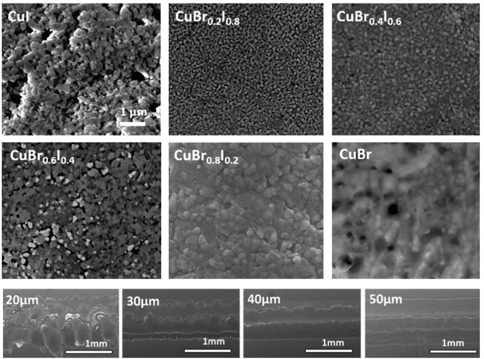 | ||
| Fig. 3 Scanning Electron Microscopy (SEM) micrographs of printed CuI, Cu0.2I0.8, CuBr0.4I0.6, and CuBr0.6I0.4 Cu0.2I0.8, CuBr, with the corresponding image at the bottom with various drop spacings for CuBr0.4I0.6. | ||
A transistor with a bottom gate and top contact structure with CuBrxI1−x printed as an active layer is shown in Fig. 4a. The interdigitated gold electrode had a 10 mm channel length and 20 μm width (Fig. 4a). The transfer curve for printed pristine CuI TFT (Fig. 4b) shows a high off-current and a low on/off ratio, with a corresponding output curve, as shown in Fig. S7 (ESI†). The high off-current represents the high conductance of thin film at zero gate bias, related to the intrinsic property of the film, such as high hole density and conductance. By alloying with CuBr with higher transition energy of copper vacancy, the decreased conductivity of printed channels was observed by increasing the CuBr amount (Fig. 4b). Benefiting from lowered off-current, the CuBr0.8I0.2 can go below 1 × 10⁻¹⁰. This shows that the hole density of CuBrxI1−x is tunable across a wide range via changing the amount of alloying with CuBr. In addition, the on/off ratio increases monotonically with the increasing CuBr ratio (Fig. 4c). TFTs with a Br/I ratio of 4 achieve the highest on/off ratio of 1.4 × 10⁵. This shows the ability to also tune the on/off ratio by adjusting the composition of CuBrxI1−x. The mobility of the device with x = 0.2 is higher than that of the device with a CuI channel. However, device with channel layer at x = 0.4 has significantly lower mobility. Further increasing CuBr to x = 0.6 and 0.8 results in TFTs with low mobilities of around 0.02 cm2 V−1 s−1. This observation matches the variation in the Hall-effect mobilities shown in Fig. 1c. The printed CuBr0.2I0.8 has optimal saturation mobility of 9.06 ± 1.94 cm2 V−1 s−1 with an on/off ratio of 103. With inkjet printing on the substrate pre-heated at 60 °C, the formed film could be highly oriented and textured in the lateral direction (the direction of printing). In contrast, the spin-coated film at room temperature might form randomly orientated polycrystals. We think the higher mobility can be achieved based on the improved crystal morphology. Fig. S8 (ESI†) shows biasing stability testing results. The off-drain current has been increased within two orders of magnitude after the first measurement. We believe that the adsorbed water in the channel layer might cause the observed bias instability. Further investigations are needed to verify the cause of this instability and to improve the device stability.
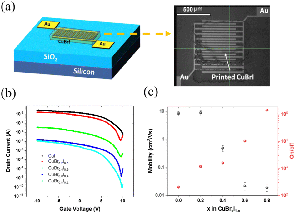 | ||
| Fig. 4 (a) Scheme and optical image of printed CuBrI TFT structure. (b) Transfer characteristics for printed CuI, CuBr0.2I0.8, CuBr0.4I0.6, CuBr0.6I0.4, and CuBr0.8I0.2 TFT. (c) The change in field-effect cm2 V−1 s−1 and on/off ratio as a function of alloy composition. | ||
Table 1 summarizes CuI-based p-channel TFTs from the literature. Solution-processed CuI thin-film transistors first reported by Chang et al. are in a US patent.55 In 2016, Choi et al. inkjet-printed CuI TFTs with a platen temperature range between room temperature and 60 °C. Devices with saturation output characteristics were obtained by applying SU8 as surface encapsulation layers. Liu et al. improved the CuI TFT performance by either using a high-k dielectric (ZrO2) layer or a cation doping method. In addition, it has been demonstrated that mobility higher than 90 cm2 V−1 s−1 can be realized with ion gel applied as an electrical gate. In this work, the CuI based device can be further improved by alloying with CuBr to adjust the channel hole density, leading to an improved and wide adjustable on/off ratio. The mobility of 9.06 ± 1.94 cm2 V−1 s−1 demonstrates the highest value reported to date for inkjet-printed CuI-based thin-film transistors.
| Device | Method | Dielectric | Temperature (°C) | On/off | Mobility | Ref. |
|---|---|---|---|---|---|---|
| CuI | Inkjet printing | SiO2 | 150 | 101–102 | 1.86 ± 1.6 | 45 |
| CuI | Spin coating | ZrO2 | Room temperature | 5 × 10² | 1.93 | 42 |
| CuI | Spin coating | Ion gel | 100 | 1.52 × 10³ | 45.12 ± 22.19 | 43 |
| CuI:Zn | Spin coating | SiO2 | 80 | 107 | 5 | 44 |
| CuBrxI1−x | Inkjet printing | SiO2 | 150 | 103–105 | 0.02–9.06 | This work |
As compared to the rigid device on glass or silicon, the textile-based TFT have features of bendability, light weight, and stretchability. Several difficulties, such as those in achieving device compatibility and stability, have been reported56 along with the appropriate method for successfully integrating textiles. In addition, the roughness of textile surface can be reduced by introducing the surface planarization technology using polyerms, such as polyurethane (PU) or polyvinylpyrrolidone (PVP).57 Benefiting from the advantage of low-temperature processing, we printed p-type Cu–Br–I-based wearable thin-film transistors as follows. PU-treated polyester was used because of its mechanical flexibility and reduced surface roughness. A schematic of the printed CuBrI TFT is shown in Fig. 5a. PVA is a water-soluble polymer that can be processed at low temperatures.58–63 PVA dielectric layers exhibit a k value between 5 and 8 at 10–106 Hz,64 comparable to solution-processed Al2O3 dielectrics.65 A vertical MIM (Metal Insulator Metal) structure was fabricated to analyze the dielectric properties of PVA by spin-coating PVA on FTO glass, followed by thermal evaporation of aluminium as the top electrode. The current–voltage curve was measured, showing a leakage current of 10−7 A at a bias of ±30 V (Fig. S6a, ESI†). We measured the Capacitance–Frequency characteristics, and the dielectric constant of coated 200 nm PVA film was calculated to be around 6.46 at 20 Hz (Fig. S6b, ESI†). A spin-coating speed of 500 RPM was used to fabricate thick PVA on polyester with leakage currents as low as 10−11 (Fig. S6c, ESI†). The complete TFT was fabricated by inkjet printing a CuBr0.2I0.8 channel layer on top of the above PVA dielectric layer, followed by thermal evaporation of gold layer as a source and drain (Fig. 5a). Unlike the device on interdigitated electrodes, the typical 2 parallel electrodes were made to test the PVA dielectric layer capability. Therefore, a dropped drain current from the transfer curve is expected. The low-temperature post-deposition annealing at 60 °C prevents thermal damage of the polyester. The TFT's electrical characteristics show typical output curves for drain currents ranging from 0 to −15 V (Fig. 5b). The transfer curve (Fig. 5c) shows a p-type response with a low leakage current from the TFT. The non-saturation region was observed in the output curve; this result is likely caused by the presence of adsorbed water on the film since our devices were fabricated under ambient conditions and Cu(Br,I) is moisture sensitive.
 | ||
| Fig. 5 (a) Side view and top view of printed CuBrI TFT on textile. (b) Output characteristic curves of printed CuBr0.2I0.8 TFTs. (c) Transfer characteristic curves of printed CuBr0.2I0.8 TFTs. | ||
4. Conclusions
This work develops printable inks consisting of mixtures of binary CuBr and CuI salts that form crystalline Cu (BrxI1−x) alloys after printing and annealing at a low temperature of 60 °C. The precursor inks have good jetting ability and are compatible with a typical inkjet printhead. The printed films show targeted elemental composition and crystal structures as dictated by the designed ink stoichiometry. Increasing the amount of CuBr reduces the carrier density of the films due to the higher energy of formation of vacancies in CuBr than in CuI. The carrier mobility drops due to the lower hole mobility of CuBr, thanks to the narrower spread of the bromide 4p-orbitals in CuBr than the spread of iodine 5p-orbitals in CuI.46,52,53 TFTs fabricated using CuBr0.2I0.8 channels yield an on/off ratio up to 103 and a high mobility of 9.06 ± 1.94 cm2 V−1 s−1, with on/off ratios as high as 105 possible with lower mobilities. This performance is comparable to that achieved by other solution-based processing methods for Cu oxide semiconductors, but without needing the high processing temperatures (few 100 °C) that make these other methods incompatible with inexpensive but thermally sensitive substrates that are beginning to dominate wearable electronics. This low-temperature printing capability is combined with a PVA dielectric layer to fabricate a functioning p-type TFT on polyester fabric without thermally damaging the fabric. This shows the potential of our approach for printing high-performance wearable complementary circuits.Conflicts of interest
There are no conflicts to declare.Acknowledgements
This work was supported by the US National Science Foundation [CMMI# 1537196, CBET# 1449383, CMMI# 2001081, ECC# 1542101] and the Walmart Manufacturing Innovation Foundation. The author also thanks Professor John Labram, Jeffrey A. Dhas and Hsin-Mei Kao at Oregon State University for the facility support and electrical measurements and the XPS measurement by Dr Rafick Addou from the NNCI facilities.Notes and references
- D. B. Mitzi, L. L. Kosbar, C. E. Murray, M. Copel and A. Afzali, Nature, 2004, 428, 299–303 CrossRef CAS PubMed.
- D. V. Talapin and C. B. Murray, Science, 2005, 310, 86–89 CrossRef CAS PubMed.
- H. Sirringhaus, Adv. Mater., 2005, 17, 2411–2425 CrossRef CAS.
- K. K. Banger, Y. Yamashita, K. Mori, R. L. Peterson, T. Leedham, J. Rickard and H. Sirringhaus, Nat. Mater., 2011, 10, 45–50 CrossRef CAS PubMed.
- D. H. Lee, Y. J. Chang, G. S. Herman and C. H. Chang, Adv. Mater., 2007, 19, 843–847 CrossRef CAS.
- C.-H. Choi, L.-Y. Lin, C.-C. Cheng and C. Chang, ECS J. Solid State Sci. Technol., 2015, 4, P3044–P3051 CrossRef CAS.
- J. Park and J. Moon, Langmuir, 2006, 22, 3506–3513 CrossRef CAS PubMed.
- D. Jang, D. Kim and J. Moon, Langmuir, 2009, 25, 2629–2635 CrossRef CAS PubMed.
- D. Kim, S. Jeong, B. K. Park and J. Moon, Appl. Phys. Lett., 2006, 89, 264101 CrossRef.
- E. Tekin, P. J. Smith and U. S. Schubert, Soft Matter, 2008, 4, 703–713 RSC.
- C. Avis, H. R. Hwang and J. Jang, ACS Appl. Mater. Interfaces, 2014, 6, 10941–10945 CrossRef CAS PubMed.
- J. W. Hennek, Y. Xia, K. Everaerts, M. C. Hersam, A. Facchetti and T. J. Marks, ACS Appl. Mater. Interfaces, 2012, 4, 1614–1619 CrossRef CAS PubMed.
- K. Woo, C. Bae, Y. Jeong, D. Kim and J. Moon, J. Mater. Chem., 2010, 20, 3877–3882 RSC.
- J. H. Cho, J. Lee, Y. Xia, B. Kim, Y. He, M. J. Renn, T. P. Lodge and C. Daniel Frisbie, Nat. Mater., 2008, 7, 900–906 CrossRef CAS PubMed.
- D. H. Lee, Y. J. Chang, W. Stickle and C. H. Chang, Electrochem. Solid-State Lett., 2007, 10, 51–54 CrossRef.
- Z. Wang, P. K. Nayak, J. A. Caraveo-Frescas and H. N. Alshareef, Adv. Mater., 2016, 28, 3831–3892 CrossRef CAS PubMed.
- S. Y. Kim, C. H. Ahn, J. H. Lee, Y. H. Kwon, S. Hwang, J. Y. Lee and H. K. Cho, ACS Appl. Mater. Interfaces, 2013, 5, 2417–2421 CrossRef CAS PubMed.
- J.-M. Yun, J. Mater. Chem., 2013, 1, 3777 CAS.
- P. Pattanasattayavong, S. Thomas, G. Adamopoulos, M. A. McLachlan and T. D. Anthopoulos, Appl. Phys. Lett., 2013, 102, 163505 CrossRef.
- J. Jang, S. Chung, H. Kang and V. Subramanian, Thin Solid Films, 2016, 600, 157–161 CrossRef CAS.
- A. Liu, S. Nie, G. Liu, H. Zhu, C. Zhu, B. Shin, E. Fortunato, R. Martins and F. Shan, J. Mater. Chem. C, 2017, 5, 2524–2530 RSC.
- A. Liu, G. Liu, H. Zhu, H. Song, B. Shin, E. Fortunato, R. Martins and F. Shan, Adv. Funct. Mater., 2015, 25, 7180–7188 CrossRef CAS.
- K. Okamura, B. Nasr, R. A. Brand and H. Hahn, J. Mater. Chem., 2012, 22, 4607–4610 RSC.
- F. Shan, A. Liu, H. Zhu, W. Kong, J. Liu, B. Shin, E. Fortunato, R. Martins and G. Liu, J. Mater. Chem. C, 2016, 4, 9438–9444 RSC.
- T. Lin, X. Li and J. Jang, Appl. Phys. Lett., 2016, 108, 233503 CrossRef.
- A. Liu, G. Liu, H. Zhu, B. Shin, E. Fortunato, R. Martins and F. Shan, Appl. Phys. Lett., 2016, 108, 233506 CrossRef.
- Y. Li, C. Liu, G. Wang and Y. Pei, Semicond. Sci. Technol., 2017, 32, 085004 CrossRef.
- S. Nie, A. Liu, Y. Meng, B. Shin, G. Liu and F. Shan, J. Mater. Chem. C, 2018, 6, 1393–1398 RSC.
- C. Wang, H. Zhu, Y. Meng, S. Nie, Y. Zhao, B. Shin, E. Fortunato, R. Martins, F. Shan and G. Liu, IEEE Trans. Electron Devices, 2019, 66, 1458–1463 CAS.
- M. Vaseem, A. R. Hong, R. T. Kim and Y. B. Hahn, J. Mater. Chem. C, 2013, 1, 2112–2120 RSC.
- S. K. Garlapati, T. T. Baby, S. Dehm, M. Hammad, V. S. K. Chakravadhanula, R. Kruk, H. Hahn and S. Dasgupta, Small, 2015, 11, 3591–3596 CrossRef CAS PubMed.
- H. Hu, J. Zhu, M. Chen, T. Guo and F. Li, Appl. Surf. Sci., 2018, 441, 295–302 CrossRef CAS.
- D. B. Mitzi, M. Copel and C. E. Murray, Adv. Mater., 2006, 18, 2448–2452 CrossRef CAS.
- D. J. Milliron, D. B. Mitzi, M. Copel and C. E. Murray, Chem. Mater., 2006, 18, 581–590 CrossRef.
- N. Wijeyasinghe, L. Tsetseris, A. Regoutz, W. Y. Sit, Z. Fei, T. Du, X. Wang, M. A. McLachlan, G. Vourlias, P. A. Patsalas, D. J. Payne, M. Heeney and T. D. Anthopoulos, Adv. Funct. Mater., 2018, 28, 1–16 Search PubMed.
- N. Wijeyasinghe, F. Eisner, L. Tsetseris, Y. H. Lin, A. Seitkhan, J. Li, F. Yan, O. Solomeshch, N. Tessler, P. Patsalas and T. D. Anthopoulos, Adv. Funct. Mater., 2018, 28, 1–14 Search PubMed.
- P. Pattanasattayavong, N. Yaacobi-Gross, K. Zhao, G. O. N. Ndjawa, J. Li, F. Yan, B. C. O’Regan, A. Amassian and T. D. Anthopoulos, Adv. Mater., 2013, 25, 1504–1509 CrossRef CAS PubMed.
- L. Petti, P. Pattanasattayavong, Y. H. Lin, N. Münzenrieder, G. Cantarella, N. Yaacobi-Gross, F. Yan, G. Tröster and T. D. Anthopoulos, Appl. Phys. Lett., 2017, 110, 113504 CrossRef.
- Y. Ji, H. J. Lee, S. Lee, K. G. Cho, K. H. Lee and K. Hong, Adv. Mater. Interfaces, 2019, 6(19), 1900883 CrossRef CAS.
- Y. Ji, S. Lee, H. J. Lee, K. S. Choi, C. Jeon, K. H. Lee and K. Hong, J. Mater. Chem. C, 2020, 8, 5587–5593 RSC.
- S. Baig, A. D. Hendsbee, P. Kumar, S. Ahmed and Y. Li, J. Mater. Chem. C, 2019, 7, 14543–14554 RSC.
- A. Liu, H. Zhu, W. T. Park, S. J. Kang, Y. Xu, M. G. Kim and Y. Y. Noh, Adv. Mater., 2018, 30, 1–7 Search PubMed.
- H. J. Lee, S. Lee, Y. Ji, K. G. Cho, K. S. Choi, C. Jeon, K. H. Lee and K. Hong, ACS Appl. Mater. Interfaces, 2019, 11, 40243–40251 CrossRef CAS PubMed.
- A. Liu, H. Zhu, W. T. Park, S. J. Kim, H. Kim, M. G. Kim and Y. Y. Noh, Nat. Commun., 2020, 11, 1–8 CrossRef PubMed.
- C. H. Choi, J. Y. Gorecki, Z. Fang, M. Allen, S. Li, L. Y. Lin, C. C. Cheng and C. H. Chang, J. Mater. Chem. C, 2016, 4, 10309–10314 RSC.
- N. Yamada, Y. Tanida, H. Murata, T. Kondo and S. Yoshida, Adv. Funct. Mater., 2020, 2003096, 1–10 Search PubMed.
- F. Guo, Z. Lu, D. Mohanty, T. Wang, I. B. Bhat, S. Zhang, S. Shi, M. A. Washington, G.-C. Wang and T.-M. Lu, Mater. Res. Lett., 2017, 3831, 1–7 Search PubMed.
- T. Harada, S. Tao, T. Imamura, K. Moriya, N. Saito and K. Tanaka, Jpn. J. Appl. Phys., 2018, 57, 02CB05 CrossRef.
- I. Tanaka, K. Sugimoto, D. Kim, H. Nishimura and M. Nakayama, Int. J. Mod. Phys. B, 2001, 15, 3977 CrossRef CAS.
- J. Wager, Science, 2003, 300, 1245–1246 CrossRef CAS PubMed.
- P. Post, L. Wurlitzer, W. Maus-Friedrichs and A. P. Weber, Nanomaterials, 2018, 8, 1–19 CrossRef PubMed.
- K. V. Rajani, S. Daniels, M. Rahman, A. Cowley and P. J. McNally, Mater. Lett., 2013, 111, 63–66 CrossRef CAS.
- N. Yamada, R. Ino and Y. Ninomiya, Chem. Mater., 2016, 28, 4971–4981 CrossRef CAS.
- M. M. Lee, J. Teuscher, T. Miyasaka, T. N. Murakami and H. J. Snaith, Science, 2012, 338, 643–647 CrossRef CAS PubMed.
- C.-H. Chang, D. H. Lee and Y. J. Chang, US Pat., 2014, 8679587 Search PubMed.
- T. Carey, S. Cacovich, G. Divitini, J. Ren, A. Mansouri, J. M. Kim, C. Wang, C. Ducati, R. Sordan and F. Torrisi, Nat. Commun., 2017, 8, 1202 CrossRef PubMed.
- T. Carey, S. Cacovich, G. Divitini, J. Ren, A. Mansouri, J. M. Kim, C. Wang, C. Ducati, R. Sordan and F. Torrisi, Nat. Commun., 2017, 8(1), 1202 CrossRef PubMed.
- M. Wang, H. Wei, Y. Wu, C. Yang, P. Han, F. Juan, Y. Chen, F. Xu and B. Cao, Phys. B, 2019, 573, 45–48 CrossRef CAS.
- T. Da Tsai, J. W. Chang, T. C. Wen and T. F. Guo, Adv. Funct. Mater., 2013, 23, 4206–4214 CrossRef.
- W. Sun, J. Zhao, S. Chen, X. Guo and Q. Zhang, Synth. Met., 2019, 250, 73–78 CrossRef CAS.
- D. Panigrahi, S. Kumar and A. Dhar, Org. Electron., 2019, 65, 193–200 CrossRef CAS.
- S. H. Jin, J. S. Yu, C. A. Lee, J. W. Kim, B. G. Park and J. D. Lee, J. Korean Phys. Soc., 2004, 44, 181–184 CAS.
- S. Park, H. Y. Chang, S. Rahimi, A. L. Lee, L. Tao and D. Akinwande, Adv. Electron. Mater., 2018, 4, 1–7 CrossRef.
- B. Wang, W. Huang, L. Chi, M. Al-Hashimi, T. J. Marks and A. Facchetti, Chem. Rev., 2018, 118, 5690–5754 CrossRef CAS PubMed.
- J. W. Jo, J. Kim, K. T. Kim, J. G. Kang, M. G. Kim, K. H. Kim, H. Ko, Y. H. Kim and S. K. Park, Adv. Mater., 2015, 27, 1182–1188 CrossRef CAS PubMed.
Footnote |
| † Electronic supplementary information (ESI) available. See DOI: https://doi.org/10.1039/d2ma00425a |
| This journal is © The Royal Society of Chemistry 2022 |