
 Open Access Article
 This Open Access Article is licensed under a
 Creative Commons Attribution 3.0 Unported Licence
Solution-processed colloidal quantum dots for light emission
Alexander R. C. Osypiwa,
Sanghyo Lee b,
Sung-Min Jungb,
Stefano Leonic,
Peter M. Smowtona,
Bo Hou*a,
Jong Min Kimb and
Gehan A. J. Amaratunga*b
b,
Sung-Min Jungb,
Stefano Leonic,
Peter M. Smowtona,
Bo Hou*a,
Jong Min Kimb and
Gehan A. J. Amaratunga*b
aSchool of Physics and Astronomy, Cardiff University, 5 The Parade, Newport Road, Cardiff, Wales CF 24 3AA, UK. E-mail: houb6@cardiff.ac.uk
bElectrical Engineering Division, Engineering Department, University of Cambridge, 9 JJ Thomson Avenue, Cambridge, CB3 0FA, UK. E-mail: gaja1@cam.ac.uk
cSchool of Chemistry, Cardiff University, Park Place, Cardiff CF10 3AT, UK
First published on 3rd August 2022
Abstract
Quantum dots (QDs) are an emerging class of photoactive materials that exhibit extraordinary optical features. Due to the availability of narrowband emitted light from QDs, they can be used to pave the way for next-generation light-emitting devices, especially in the development of LEDs and lasers. Over recent years solution-processed colloidal QDs have been developed in pre-existing light-emitting devices such as laser scalpels, displays and data communications. QDs became mainstream in 2013, with Sony and Samsung launching QD televisions, in which photo emissive QDs are used in the backlight of LCD TVs to replace red and green phosphors. Currently, photo-emissive QD displays are the only commercially available large area QD display, with electro-emissive displays limited to smaller sizes in some smartphone devices. At the same time, lighting now accounts for 15 to 22% of the electricity used in developed countries. This highlights how fundamental artificial lighting is to humans and why more efficient light sources can significantly impact energy consumption. Throughout history, any progress in artificial lighting (with regards to chemical sources and physical phenomena) has been to increase efficiency, improve light quality and decrease costs. QDs offer this capability to advance current lighting solutions. However, even with the advancements in QD performance, there remain issues with creating heavy metal-free high-performance QD devices. This paper presents a review of colloidal QD synthesis and the reasons behind their use in light emission applications.
1. Introduction
Colloidal quantum dots have undergone remarkable progress in light based applications in recent years. The main properties that are of interest include the narrow-linewidth, high photoluminescence (PL) quantum yield (QY), which allows QDs to provide high colour saturation and reduced light/energy loss.1,2 These are highly desirable properties for lighting and display devices. QDs have also found major applications in numerous fields, such as solar cells, IoT, visible light communication, biological imaging and light emitting devices (as shown in Fig. 1). However, even with advancements in QD technologies, future development of QD light-emitting devices will face significant challenges, which are currently limiting the practical application in displays and lighting technologies. This review will provide a comprehensive summary of the fundamental physics behind how QDs work (such as mechanisms, structure and how they are made), accompanied by how current lighting works and QDs applications within the field, and the challenges currently facing QDs.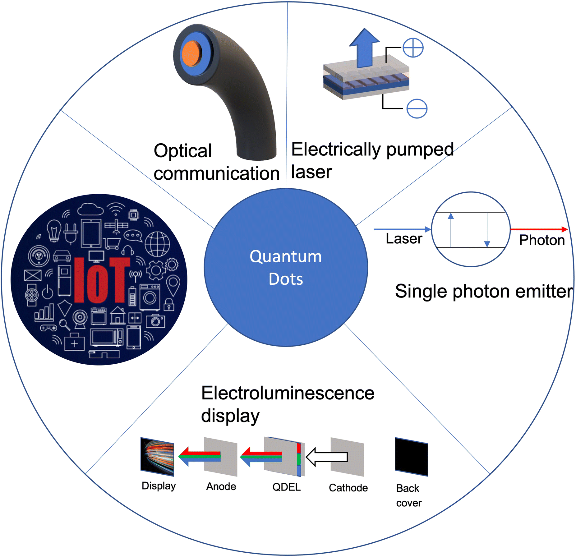 | ||
| Fig. 1 A summary and outlook of future developments for QD lighting. | ||
2. QD physics
QDs are defined as “Semiconductor particles a few nanometres in size, having optical and electronic properties that differ from bulk materials due to the effect of quantum confinement”. The quantum confinement effect dictates the optoelectronic features of solution-processed colloidal QDs. There is no defined lower limit to the size of a QD; usually, they are less than 10 nm, but even macromolecules and single impurity atoms in a crystal can be referred to as QDs. A standard QD nanocrystal structure consists of about 100–10![[thin space (1/6-em)]](https://www.rsc.org/images/entities/char_2009.gif) 000 atoms, with each QD being in the size range of 1.5–10 nm.3,4
000 atoms, with each QD being in the size range of 1.5–10 nm.3,4
2.1 Mechanisms in QDs’ light emission
Many different mechanisms can cause luminescence, but the primary mechanisms for QD lighting are photoluminescence (re-emission of light after absorbing a higher energy photon) and electroluminescence (emission of light caused by recombination of electrons and holes injected by an electrical current). The generation of luminescence in these mechanisms is linked to the energy relaxation within the material. A photon can be emitted when an electron goes from an excited state to the ground state, as seen in the Balmer series emission lines of the hydrogen atom. In molecules (Fig. 2a), the emission is determined by the energy gap between the LUMO (lowest unoccupied molecular energy state) and the HOMO (highest occupied molecular energy state). In a solid-state material (Fig. 2b), the bands of energy centred on the bonding (valence) and anti-bonding (conduction) energy states replace the discrete HOMO and LUMO energy levels. QDs (Fig. 2), by virtue of the limited number of atoms in the solid, have an intermediate energy structure with discrete energy levels rather than bands.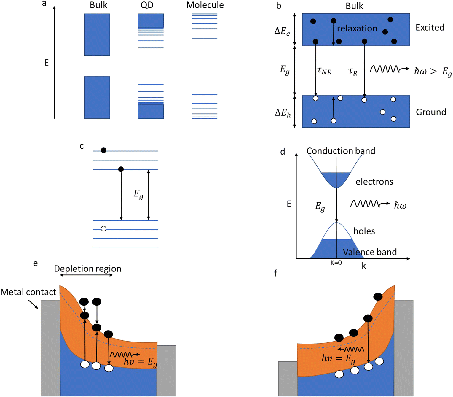 | ||
| Fig. 2 (a) The band structure of bulk, molecule and QD. (b) The mechanism of luminescence in solid materials. (c) The mechanism of luminescence in a QD. (d) The mechanism of luminescence in a semiconductor, where k is a momentum vector. (e) Type-I electroluminescence, a strong reverse bias voltage is applied through the metal contact, which regulates the injected current. The electrons reach a kinetic energy larger than the bandgap, allowing electron–hole pairs to be generated. These electron–hole pairs with energies near the band edges can then recombine radiatively by emitting light. (f) Type-II electroluminescence under strong forward bias voltage, holes are injected into the n-type semiconductor, recombining with electrons by emitting light. | ||
As shown in Fig. 2d, a photon is absorbed by an electron, allowing the excitement of a valence band electron (the most weakly binding energy state) to a conduction band state. This also creates a positively charged virtual particle, a hole, in the valence band. If an excited electron can recombine with a hole in relaxing to a lower energy state, then the reverse process of photon generation can happen. This mechanism is termed radiative emission or germinate recombination. However, it is not the only mechanism by which electrons can relax to the ground state. Electrons can lose energy in non-radiative processes such as phonon generation (thermal decay) through recombination via trap states in the energy gap (Shockley Read Hall) or three-particle energy transfer (Auger). If these non-radiative relaxation processes occur on a faster time scale than the radiative transitions, very little light will be emitted.
All luminescent materials will have a luminescent efficiency (also known as quantum yield). To find the luminescent efficiency ηR, the rate equation for the population of the excited state when non-radiative processes are possible has to be defined:
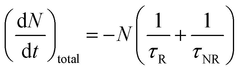
η R is given by the ratio of the radiative emission rate to the total de-excitation rate.
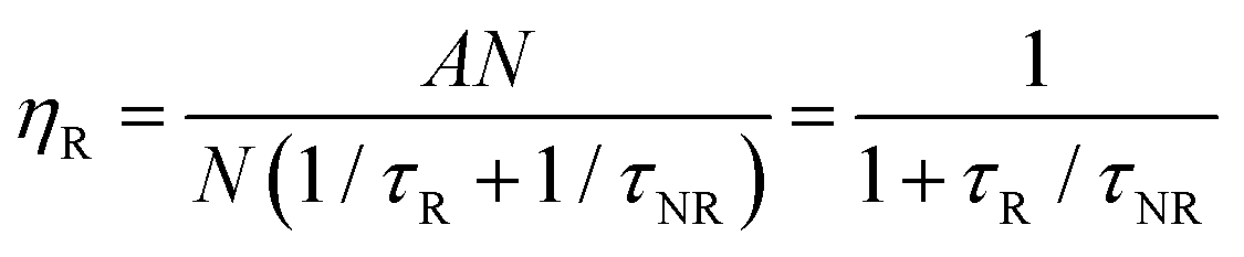
From the expression above, to achieve maximum light emission τR ≪ τNR.
Semiconductor materials can have either a direct or indirect bandgap. Fig. 1d shows the band diagram for an inter-band luminescence process in a direct gap semiconductor. Luminescence through electron-hole recombination has a short radiative lifetime, and hence the luminescence efficiency will be high.
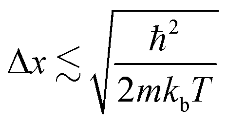
In a bulk material, possible electron energy levels are represented as bands of closely spaced energy levels present in the material, but as the material reduces in size, the discrete nature of the energy states becomes more obvious.5 This effect is known as quantum confinement (Fig. 2a). In practice, materials can be confined in 3 dimensions; if confined in 1 dimension, a quantum well is formed; in 2-dimensional confinement, a quantum wire is created; and in 3-dimensional confinement, a quantum dot is formed. Using Heisenberg's uncertainty principle, we can derive an equation for the confinement energy:
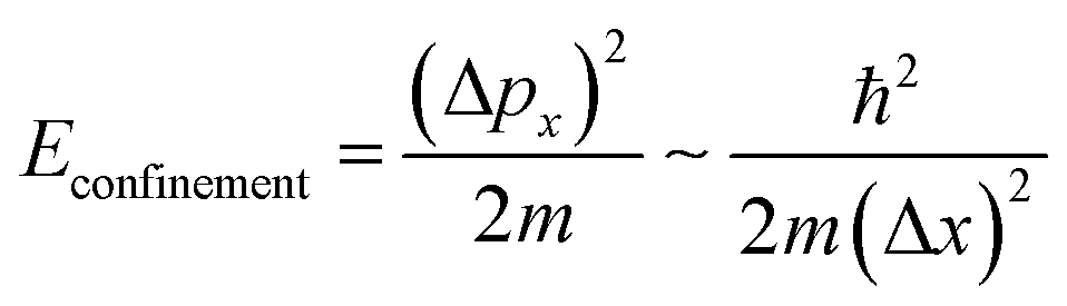
And from this we can see that size has the following effect:
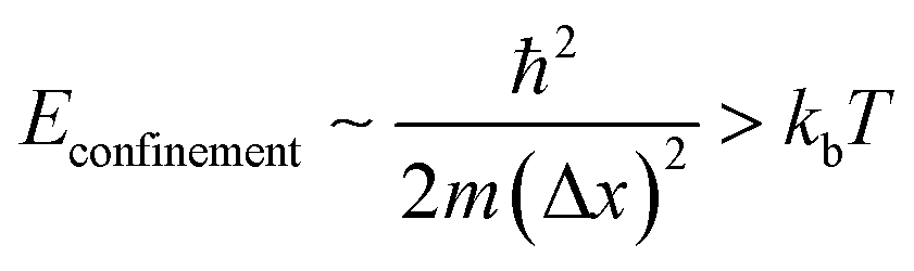
This shows that Δx must be comparable to or smaller than the de Broglie wavelength λdeB ≡ h/px for the thermal motion. The result of this is that materials are required to be of a certain size for quantum confinement to be observed; for nanoparticles such as QDs, the size is required to be between 1–10 nm to behave as a QD. Since the confinement energy of an electron in a QD can be related to the wavelength of a photon that it can absorb, the size effect can be used to control its optical properties. This means that particles can be made to emit or absorb specific wavelengths (colour) of light depending on their size.6
QDs have their electrons and holes confined in 3 dimensions (Fig. 2c), making QD a zero-dimensional structure, i.e. there are zero dimensions in which electrons are free to move. Confinement affects the energy spectrum, but it also increases the electron-hole overlap, which increases the radiative quantum efficiency. This increased overlap between the electron and hole wave functions causes the emission probability to increase due to the shortening of the radiative lifetime. Therefore, QDs have very high radiative efficiency making them suitable as an emissive layer for light-emitting devices.
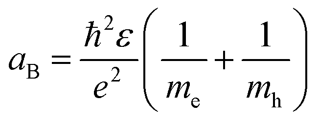
As shown in Fig. 1e and f, the mechanism in QDs that causes the luminescence is a recombination of electron–hole pairs (sometimes known as exciton decay). The trapping of a photon excites an electron from the valence band into the conduction band, leaving a positive hole in its place. The excited electron is attracted to the hole due to Coulomb force, this bound state of an electron–hole pair is known as an exciton. When an exciton recombines, then a photon can be produced. For confined structures (such as QDs), excitons are responsible for the quantized energy states. In an exciton, the electron and hole will orbit each other much like in a hydrogen atom, which means that excitons will have a Bohr radius. The exciton Bohr radius is a useful parameter for evaluating the conditions for creating quantum confinement effects in a specific material.
Confinement effects must be considered as the material dimension becomes similar or smaller to the exciton Bohr radius (aB), this can be expressed as:
The variation of the QDs band gap can also be achieved by changing the material composition.7 This allows for large spectral tunability, high ambient stability, high sensitivity, and quantum efficiency with narrow spectral bandwidth. The position of the energy levels in a QD can be changed based on the size/design. The smaller the size of QDs of a given material, the smaller the wavelength of the photon produced.8 This means that quantum dots can emit particles (photon/electrons) of specific energy, making them very suitable for the creation/use of LEDs, lasers, and single-photon emitters.9 The atom-like energy states of QDs determine their unique optical properties.10 These properties include particle size-dependent wavelength of fluorescence, which is useful in making optical probes for biological and medical imaging.11
There are three main groups of QD semiconductors according to the periodic table of the elements,12 these are groups II–VI, III–V, IV–VI compound semiconductors. It is useful to classify their structures into core-type QDs: core-only (CdS and CdSe, PbS, PbSe), core and shell (CdS/ZnSe, CdSe/CdS, InAs/GaAs, InAs/InP), and core and two shells (CdSe/CdS/ZnS, CdTe/CdS/ZnS, InP/ZnSe/ZnS). The core acts as the active QD. The shells provide surface passivation/termination to the core and also further confinement by having a larger bandgap than the core as well as relaxing the lattice strains. Their properties can be tuned by changing active QD size. Most materials can be doped with other materials (impurities), which changes the bonding structure and optical properties. The doping materials are normally transition metals, and they can affect not only the optical properties but also the magnetic properties of a QD. Doping material in a QD can also offer various advantages, such as improved quantum yield (QY) and longer excited-state lifetimes.13 Quantum yield is a measure of the number of photons coming out of a materials compared to the number of photons put in, which differs from quantum efficiency which is a measure of the photons/electrons coming out compared to the electrons/photons put in.14 For imaging in biological systems high QY results in a better detection limit, and longer excited-state lifetimes are useful for overcoming background fluorescence in biological systems. The surface of the QD has a direct impact on optoelectronic properties. The presence of surface defects are largely responsible for the loss of luminescence in QDs. Techniques for reducing QD surface states include chemical etching, surface-bound ligands, and passivation with wide bandgap shell structures.15 However, complete elimination of surface states is impossible due to the incomplete ligand coordination, presence of lattice vacancies, or the remaining lattice mismatch at the core–shell interface.
2.2 Structure of a QD
QDs have outstanding excitonic optical properties (Fig. 3a–c) that depend not only on their size but also on the composition and structure. Most QDs have a core–shell structure,15 as illustrated in Fig. 3d, with a high surface to volume ratio. The surface bonds or defects can become nonradiative recombination centres which lower the QY and photoluminescence. To minimise the nonradiative recombination, an inorganic shell with a wide bandgap (such as ZnS or ZnSe) is incorporated on the surface of the QD. The core–shell structure confines excitons within the core, reducing the impact of nonradiative recombination centres on the surface. However, the mismatch in the lattice spacing of the core with shell materials results in residual defects that can act as no-radiative recombination centres. Multiple shell layers have been tested on QDs (such as CdSe, CdS, and ZnS) in order to minimise the lattice mismatch.15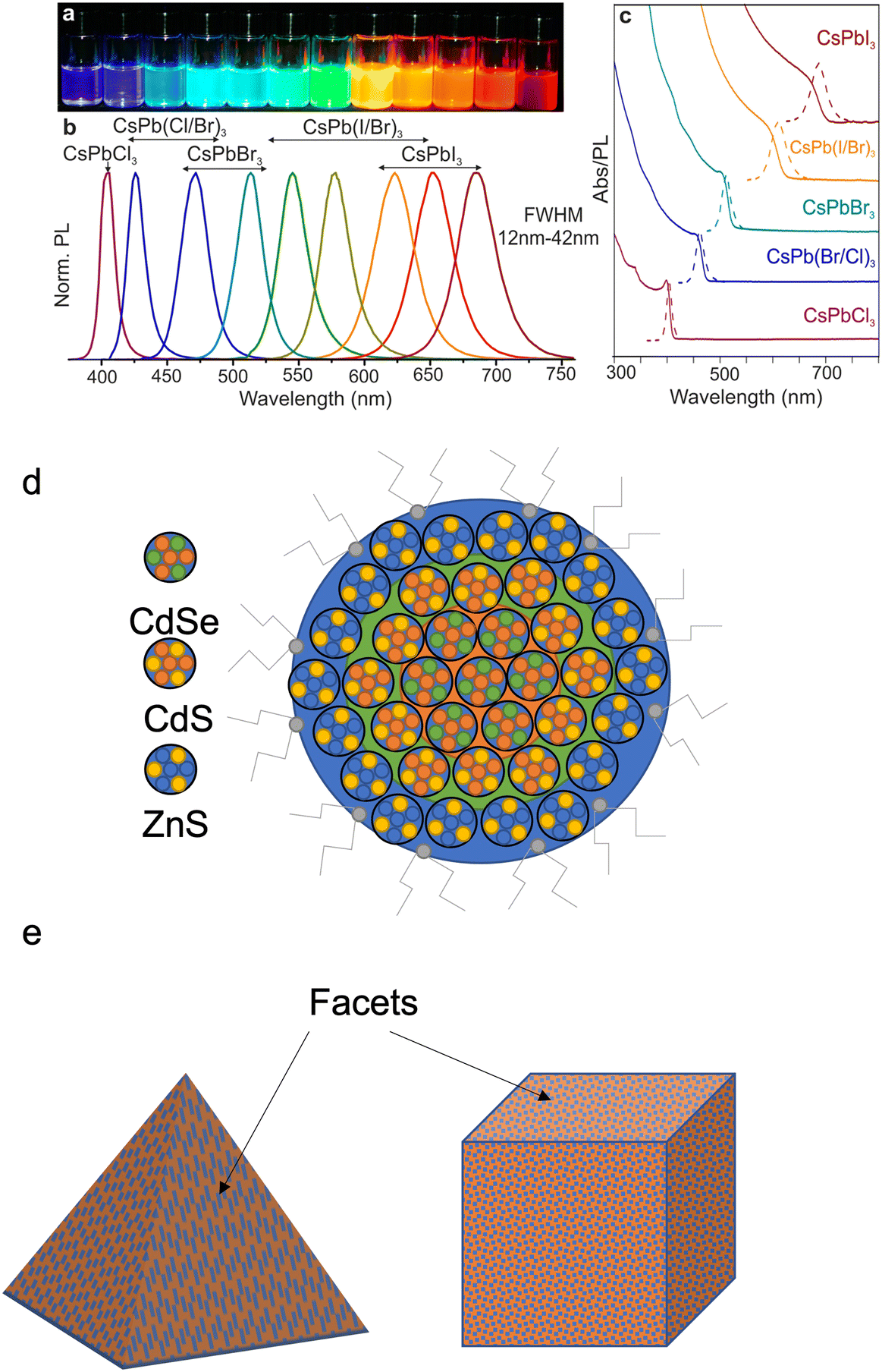 | ||
| Fig. 3 An image of different composition CsPbX3 QDs (a) under UV lamp, (b) corresponding photoluminescence spectra and (c) corresponding absorption spectra of the same QDs. Reproduced with permission.4 Copyright 2015 American Chemical Society (d) Atomic models of a core–shell structure of a QD, with the core being the CdSe QD and the CdS and ZnS forming layers around the core to improve luminescence efficiency. (e) The different types of colloidal QD structures. | ||
The shell can also passivate the QD core, improving its photo and thermal stability.16–18 The QD core–shell structures can be classified as Type 1 – where the nanocrystals have a smaller core bandgap than a shell bandgap, with the core conduction and valence band edges being located within the shell bandgap and Type 2 – where both the band edges of the core are higher than that of the shell. Studies on how the core–shell structure affects the wavefunction of QDs have found that as the shell thickness increases, the Type 1 structure can shift into a Type 2 structure. Altering the size and shape of quantum dots will change the energy spacing between the valence band and conduction band edges of the core and shell. The shell size also affects the localization of the electron and hole. With thinner shells (below 1.2 nm), the electrons and holes are localized within the core region; between 1.2–1.8 nm, the electrons remain in the core, but the holes begin to shift into the shell and can be localized in both. Above 1.8 nm, electrons are localized in the core and holes are localized in the shell, this applies for both Types 1 and 2.
All QDs are made from some form of crystal that can be grown in a certain shape (Fig. 2e). The properties of a QD are therefore not only determined by its size, composition, and core–shell structure but also by its shape. This requires a reliable manufacturing method to create large quantities of uniform QDs of a defined specification.19–22
2.3 QD synthesis
Fig. 4 shows a summary of the different methods used in making QDs. In the figure, top-down methods involve strategies based on the size reduction of bulk materials, while bottom-up methods QDs are synthesized using chemical precursors.23 This category can be subdivided into the vapour phase and wet chemical methods. In this review, we will mainly focus on wet chemical methods.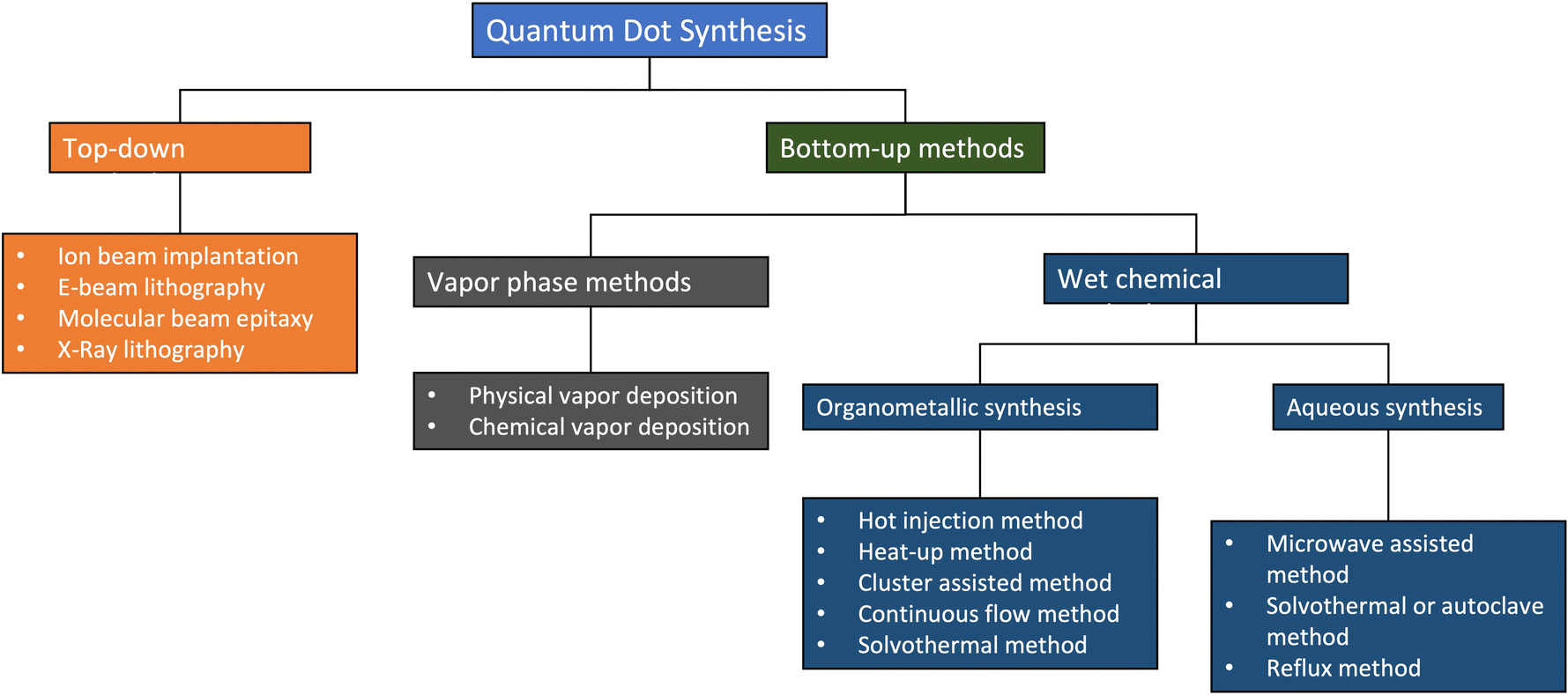 | ||
| Fig. 4 The different methods of QD synthesis. Reproduced with permission.23 Copyright 2021, MDPI. | ||
QDs that possess high photoluminescence QYs, flexible emission colour control, and solution processibility are promising for lighting systems and high-quality display applications. However, the commercialization of these QDs has been hindered by the high cost of their production. One of the ways of making QDs by wet chemical methods that have garnered significant interest is colloidal synthesis (Fig. 5a–d). These dots are made from the II–VI or III–V compound semiconductors spherical in shape. Colloidal QDs can be used either in their base solution form or in a solid-state film. Colloidal QDs are solution-processed semiconductor nanocrystals, which means that they can be dispersed on multiple different substrates. To get QDs in a solid-state, the dots can be deposited as thin films or doped into a glass.24 When synthesising QDs, there will always be a spread of particle sizes, which causes a broadening of the optical spectra. Just like molecular-beam epitaxy (MBE) and metal–organic chemical vapour deposition (MOCVD) epitaxial grown QDs (Fig. 5e and f), colloidal QDs emit photons in the wavelengths from visible light to near-infrared, with the choice of the emitted wavelength achieved through composition and sizes control (Fig. 5c).24–28 Colloidal QDs first synthesised in the 1980s were created from a similar group of materials (groups II–VI, IV–VI, I–III–VI and III–V).29 Benefits of colloidal QDs over normal epitaxial QDs include the easier realisation of QDs with more complex structures19 and synthesis through low-cost mass production chemical methods (Fig. 5d).30
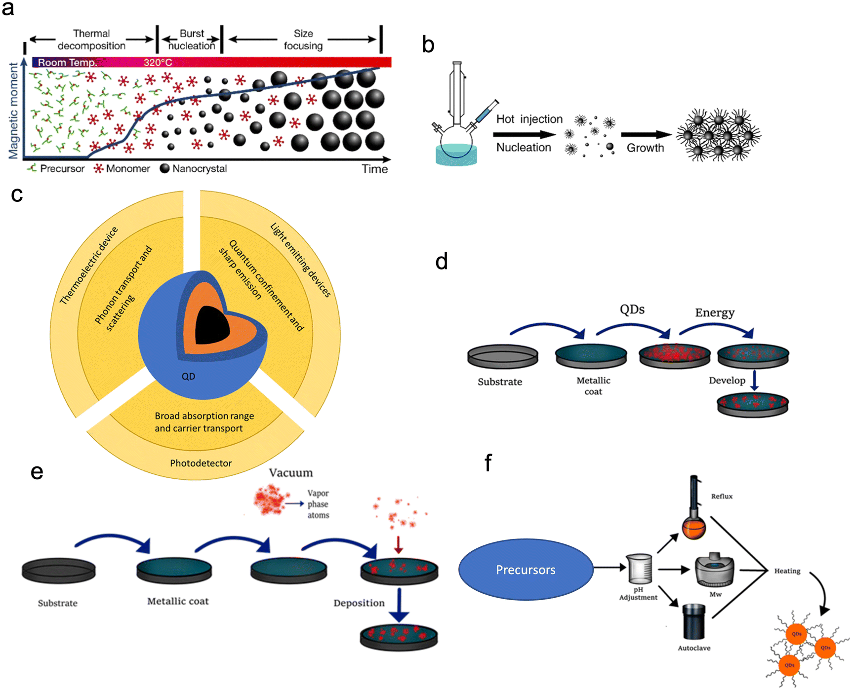 | ||
| Fig. 5 (a) Heat up method showing how the time effects the colloidal growth of QDs. (b) A typical hot injection synthesis set-up and growth. Reproduced with permission31 Copyright 2018 IOP Publishing Ltd (c) a summary of the electronic, optical, physical and structural properties of a QD and their uses. (d) The general synthesis of QDs by top-down methods. (e) The general synthesis of QDs by vapor phase methods. (f) The general synthesis of QDs by aqueous methods. Reproduced with permission23 Copyright 2021, Licensee MDPI. | ||
Typical “hot injection” organometallic colloidal synthesis of QDs (illustrated Fig. 5a and b) works by dissolving a metal precursor (such as cadmium oleate or CdO) into a coordinating organic solvent such as trioctyl phosphine oxide (TOPO) or trioctyl phosphine.32 The coordinating solvent is used to control the QD growth as it binds to the surface of the nucleating particles. An anion solution (for example, Se or S) is then injected and the solution heated.31 The longer the growth time, the larger the QDs become and the larger the wavelength of emitted photons. The growth of the QDs can be stopped by the injection of cold acetone or methanol. Since the reagents in the reaction are reactive to the air, the whole reaction has to be done under the presence of inert gases such as noble gases or nitrogen. The hot injection method is good for creating high-quality QDs, however, in order to mass-produce QDs other methods are used. One of these methods is the continuous flow method.33 The continuous flow method (Fig. 5d) is better than batch synthesis since the reaction parameters can be readily automated and controlled to achieve a more efficient process of optimization, enhance the efficiency with which the precursors are mixed, and increase scalability.
One major challenge of QDs is the integration of materials onto the complementary metal–oxide–semiconductor (CMOS) technology because the miscibility of the different QDs solutions can damage CMOS and destroy the function of isolated QD devices.34 The recently developed solvent-free dry transfer method offers the opportunity of integrating QDs onto CMOS.25,26 CMOS technology can have integrated photonic detection and electronic signal processing functions (e.g. CMOS image sensors/cameras) which are cost-effective. QDs can also have photoemission properties that can enhance CMOS photonics if they can be integrated into a CMOS process.25 The advantage that QDs have over other semiconductor materials is their size, tuneable bandgap and compatibility with different substrates. Due to the solution-processed nature of QDs, they are easy to manufacture and integrate and hence have found use in many different electronic devices such as lasers, light-emitting diodes (LEDs),29,30,32,35–37 batteries,31 solar cells and photodetectors,33,34,38–41 see Fig. 5c. Their application to multicolour imaging and imaging in the near-IR window42 has also attracted much interest. In conjunction with these production methods, etching on the chips is another way to help promote QD deposition in certain regions on the chip. This is useful as due to the size of QDs it's hard to determine where on the chip they are deposited until you can get a luminescence emission image of the chip.43
Post synthesis, QDs still need to be deposited/applied/patterned on a device or substrate (Fig. 5a–g). This can be achieved using multiple different methods such as spin coating, epitaxy and lithography.44 Typically, QDs get changed from the solution to thin films by different deposition methods such as spin coating, spray coating, roll-to-roll printing, inkjet printing, dip coating and transfer printing.26,29,30,45,46 These deposition methods normally make the manufacturing of QD based devices facile and versatile.
The self-assembly feature of QDs results from the way the solution is evaporated (Fig. 6a–g). When the QDs have a monodispersed structure, the evaporation of the solution can be used to create superstructures. Another added benefit of using QDs for this process is that when you tune the energy levels of QDs, interparticle coupling and structural arrangement can be used to modify the electronic structure of the structures.
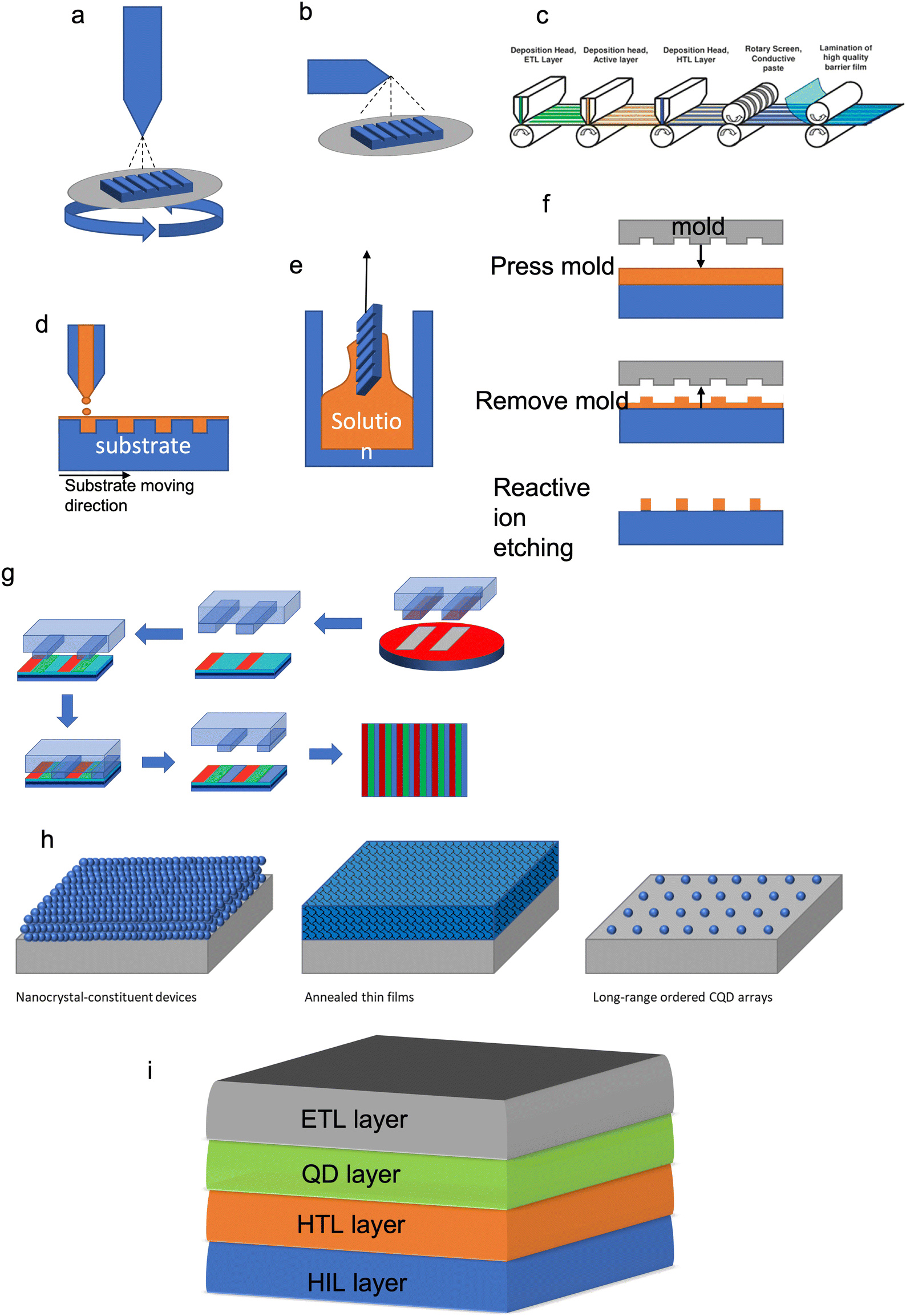 | ||
| Fig. 6 A summary of different QD deposition techniques of (a) spin coating, (b) spray coating, (c) roll-to-roll printing. Reproduced with permission.47 Copyright 2016 Author(s), (d) inkjet printing, (e) dip coating, (f) lithography and (g) transfer printing. (h) The assembly of QDs using different methods. (i) A generic thin film cross-section design for a QD LED. | ||
When these structures are made, there will be gaps between the QDs. These gaps allow for the diffusion of gaseous materials, which can be used as sites for atomic layer deposition, allowing a semiconductor oxide to be included in the QDs. Such oxide filling of the gaps creates a surface layer that protects from QD oxidation and creates a heterojunction that improves the charge carrier transport. Alternatively, QDs can be deposited with a second phase, either using a sol–gel or solution process method. This enables the creation of composites with QDs, such as QD–polymer composites, which improve the emission repeatability and stability. Perovskites can also be used with QDs; using a lattice-matched perovskite an epitaxial film can be grown around the QDs, which will improve the surface passivation and charge carrier mobility. Epitaxial films will also help to protect against agglomeration and oxidation.
Illustrated schematics in Fig. 6h are the different deposition methods resulting in the formation of other structures, which changes the use of the QDs. The nanocrystal-constituent device is made by densely packing a solution phase into a thin film using solution-processed deposition methods. The annealed thin film is created by the sintering of QDs, causing the film to become a polycrystalline solid. The long-range ordered QD arrays are created using the self-assembly of monodispersed QDs.
While chemically synthesized QDs offer a much easier method of scale-up fabrication and integration onto nanoscale architectures (e.g. single-photon emitters),48 the disadvantage is that the properties of QDs depend on the surface chemical composition and the structure, which cannot be fully controlled. The control of size and shape uniformity of QDs is needed for high quality (Fig. 3e). This can be achieved by controlling the precursor stoichiometry (this is the balance between the amount of reactants and products in the reaction) or using size-selective precipitation to separate the nanoparticles.15,47 This will produce QDs with a narrow absorption linewidth and small Stokes shift. The flexible surface structure of QDs allows for the creation of building blocks for a range of optoelectronic applications. A typical QD electroluminescence light emission device (Fig. 6i) is therefore created using a lay-by-layer quaternary structure (i.e., spin coating) that has an anode/hole injection layer (HIL)/hole transport layer (HTL)/quantum-dot or an emissive layer/electron transport layer (ETL)/cathode. When a current is applied to a device, electrons will go into the electron transport layer, and holes will be created in the hole injection layer. The charge carriers then move through the device, as the speed of holes and electrons are different, so the charge transport materials (Table 1) and structure of the device are designed to have the charge carriers arrive at the same time in the emissive QD layer (e.g., charge balance). Device efficiency is defined as the ratio of the energy emitted out of the QD device to the put into the device, per unit time, termed external quantum efficiency (EQE).43 In order to create QD devices with optimal efficiency, the carrier mobility and band gap energy levels for each layer have to be considered, for an ideal device the band gap energy of each layer should be similar and have a high carrier mobility.2 One practical way is via using inorganic materials since these materials not only have ideal band gap energies and high carrier mobility, but also exhibit higher device stability than organic counter parts. To reduce the band gap energy mismatch and carrier mobility between the layers several strategies have been used, such as chemical doping or surface modification to alter the work function of electron transport materials (such as ZnO and TiO2), band-structure tailoring of QDs for hole-injection improvement and the use of buffer layers (such as TFB) which promote electron transport and confine holes.49,50
Inorganic halide perovskite quantum dots (IPQDs) are alternatives to the colloidal dots discussed so far (Fig. 3a–c), however perovskite quantum dots are sometimes too large to be considered QDs and should instead be sean as nanocrystals. These perovskite systems have shown a comparable and, in some cases, even better performance than compound semiconductor QDs (i.e. groups II–VI, III–V) for many different applications. Perovskite material can also be used with QDs. Using a lattice-matched perovskite a colloidal epitaxial film can be grown around the QDs, which will improve the surface passivation and charge carrier mobility. Colloidal epitaxial films will also help to protect against agglomeration and oxidation. IPQDs have the advantage of being able to be made at room temperature, which could lead to cost-effective applications in lighting and displays.56–63
3. Colour
When the visible part of the electromagnetic spectrum (light) impinges on an object, part of the spectrum is absorbed, part is reflected. The human brain senses the reflected wavelength combinations through the eyes and translates them into the phenomenon termed colour. The photoreceptor cells in the retinas of the eyes transmit signals to the brain. As shown in Fig. 7a, humans have three types of cones (the photoreceptor cells in the eye), leading to the trichromatic theory of colour. This causes a colour perception that only responds to 3 different wavelengths (trichromatic colour vision). These are, short (S) – blue spectrum (absorption peak ≈ 445 nm), medium (M) – green spectrum (absorption peak ≈ 535 nm) and long (L) – red spectrum (absorption peak ≈ 565 nm). This theory was proposed by Thomas Young and Hermann von Helmholtz in the 19th century, which has led to the application of the RGB (red, green, blue) colour model64 and the trichromatic theory.65 Due to the broad nature of these peaks, the L peak illustrated in Fig. 7a is known as the red peak, which actually peaks in the greenish-yellow wavelength (Fig. 7b). There are no definite boundaries between the colours.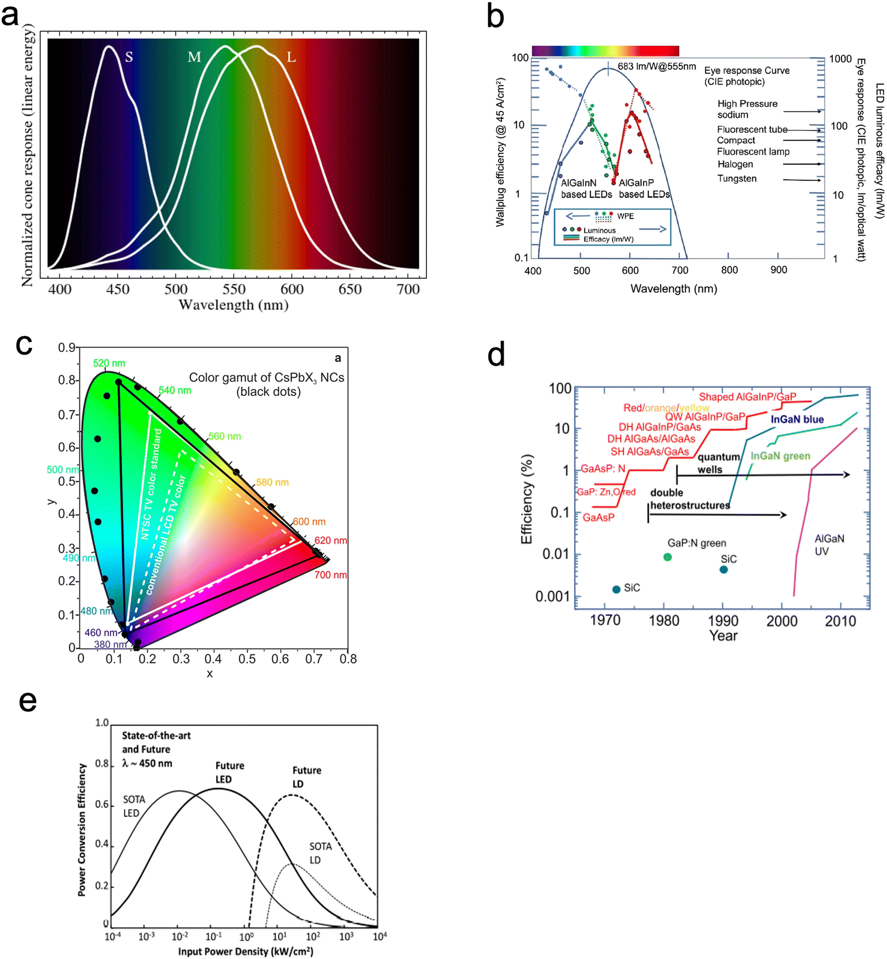 | ||
| Fig. 7 (a) The different visible light spectra and peaks which the human eye perceives. Spectral sensitivities of L-cones, M-cones and S-cones. Reproduced with permission,66 Copyright 2016 Mysore A et al. (b) The Wallplug efficiency, luminous efficiency and human eye response curve. Reproduced with permission.67 Copyright 2018, Elsevier Masson SAS. (c) Emission from CsPbX3 NCs (black data points) plotted on CEI chromaticity coordinates and compared to most common colour standards (LCD TV, dashed white triangle, and NTSC TV, solid white triangle).4 (d) The evolution of quantum efficiency of RGB and UV LEDs. Reproduced with permission.67 Copyright 2018, Elsevier Masson SAS. (g) A comparison between LED and laser diodes (LD) and the expected future performance. Reproduced with permission.67 Copyright 2018, Elsevier Masson SAS. | ||
The RGB colour model is based on the way humans perceive the colour in the light. When a colour is observed, it's a combination of the three colours, red, green and blue, with different intensities (Fig. 7b). When the three colours (RGB) are mixed with equal intensity white light is perceived (Fig. 7c).53 This, however, does not rule out the generation of perceived white light through the combination of other relative colour mixes through expansion of the RGB primary set (Fig. 7b and d – CIE 1931 colour space).66 However, the colour palette is not limited to RGB in printed colours, which rely on preferential reflection from pigments (e.g. inkjet printer). When we observe a colour, e.g. yellow, it triggers our perception using the relevant cone for the yellow.68 To date, the generation of the visible light spectrum through artificial approaches, such as in lighting, displays, and filtered white light projection, has been achieved through the combination of RGB primary colours (Fig. 7e). An added complication is that the appearance of colour can vary based on the ambient light, which means that it can be affected by the time of day, lighting in the ambient, and many other factors. For this reason, it is essential to use digital tools for colour control in artificial light to ensure objective colour perception is measured.53
QDs light-emitting devices can be made with different wavelengths. Devices can be made with just a emissive single colour wavelength RGB QDs or can have some combination of the RGB dots to create different colour LEDs (Fig. 7b and f). QDs offer an unprecedented opportunity to explore colour/light generation to match optimum human perception and well-being, through for example managing circadian rhythms (Fig. 7f).
4. Electronic lighting
As discussed previously (Fig. 2e and f), electroluminescence is the direct conversion of electricity into luminous energy, which was discovered (by accident) in 1907 by Henry J Round. Working with carborundum, he noticed a yellowish light at low voltage and yellow, light green, orange and blue lights at higher voltages on various points of different crystals. This was distinct from the electricity to light conversion through thermoluminescence of the Edison incandescent light bulb where only a single colour temperature is seen.69,70 Later rediscovered by Losev in 1922, two mechanisms of electroluminescence were identified; (i) by excitation of the semiconductor under high reverse bias voltage (also known as Type-I luminescence, Fig. 2e) and (ii) direct current injection in the semiconductor (as in LEDs today) and termed as Type-II luminescence, Fig. 2f.70 Losev is considered to be the inventor of the LED.71,72 In 1928 Losev also identified the physical mechanism of emission being quanta of energy or photons.LEDs are so universally used mainly due to their high efficiency, ease of use, and reliability.54 The high efficiency partly occurs because, unlike filament light bulbs, only light in the visible spectrum is emitted, which also means that LEDs do not generate as much heat (Fig. 7c). Fig. 7e is a graph that illustrates how the efficiency of visible and UV LEDs has improved over time, and Fig. 8 shows the QD research timeline since 1980.73 Improvements were made when the active light-emitting region was sandwiched between materials with a higher bandgap region. This had the effect of avoiding the emitted light from being reabsorbed on exiting the device. It also causes the electrons and holes to be more confined in the smaller bandgap QD layer analogous to that in the III–V heterostructure device. This results in an increase in the radiative recombination rate.
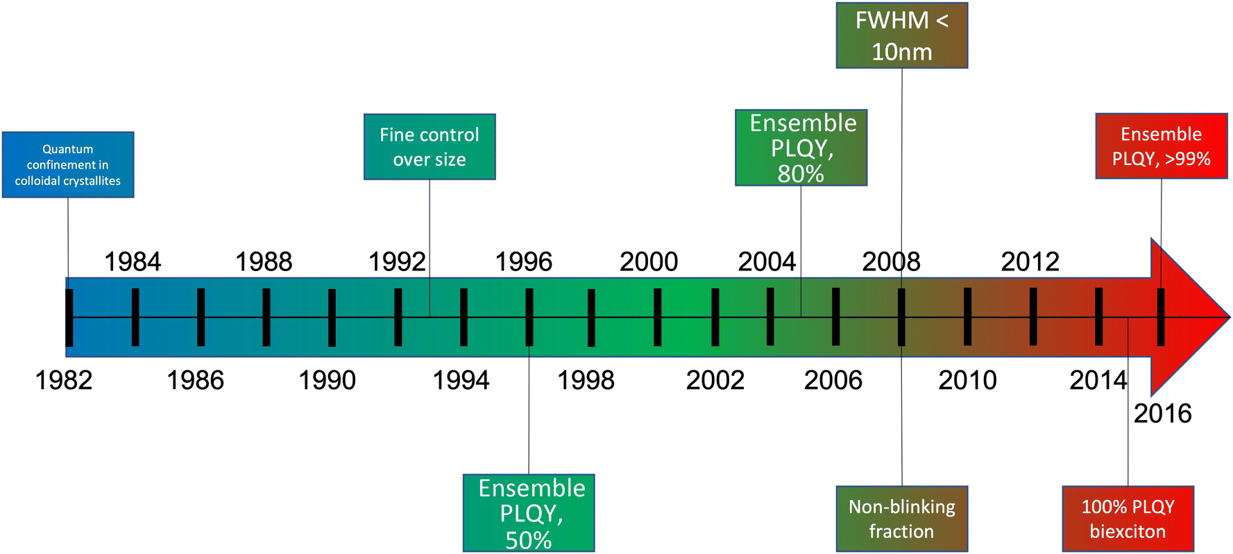 | ||
| Fig. 8 The development and advancement in colloidal QDs since 1980. | ||
5. QD lighting
QDs offer seamless tunability of the optical bandgap from the UV to the mid-infrared (IR), which makes them useful in a wide range of light-based applications. The main features of QD light emission that make them desirable are the high quantum efficiency (e.g. high QY), the tunability and narrow bandwidth of the emitted photons (i.e. full width at half maximum, FWHM). QDs are now being used in a range of light-emitting devices (LED, laser and single-photon emitters), and the main challenge now is integrating QDs into existing devices. In lighting applications, the primary device employed is the LED.QDs are used in light-emitting devices because they are both photoluminescent and electroluminescent. In QLED TVs, first launched by Samsung and LG in 2015, red and green QD emission in photoluminescent mode is combined with a blue light emitting GaN LED to obtain the white backlight of an LCD TV. The blue light from the GaN LED is absorbed by the QDs and down-converted to red and green light. In this mechanism, the QDs replace the traditional phosphor, which was previously used for down-conversion of the blue LED light due to the higher quantum efficiency of the photoluminescent QDs.
Conventional white LEDs have difficulty maintaining high luminous efficiency and high colour quality simultaneously since the red luminophores must have relatively narrow emission spectra to avoid photon loss as infrared emission. QDs do not have this limitation, due to the intrinsic narrow spectral emission (∼30 nm FWHM). QDs, therefore, enable higher colour quality and lower power consumption in lighting sources.67,74 The most efficient materials for QD light emission applications are CdSe, InP and CuInZnS based semiconductor nanocrystals. Cd based white light LEDs (WQLEDs) have been reported to have a high current efficiency (CE) of 60.4 cd A−1 and external quantum efficiency (EQE) of 27.3% at a luminance of 100000 cd m2.75 Despite the performance of Cd-based QDs, the toxicity of cadmium makes it environmentally unattractive, and its widespread use and commercialisation have not occurred. This has pushed the development of other materials such as InP and CuInZnS based QDs.9,34,76–80 The lifetime of the QD LED devices has also significantly improved over the years, increasing from 100 hours to upwards of 1400 hours. Lifetime of an LED is based on the time it takes for the luminescence intensity to decay to a specific level.1,2,49
Electroluminescent QDs are especially good for use in LEDs as they produce pure monochromatic red, green, and blue light. Due to how humans perceive colour (RGB colour theory, Fig. 7), QLEDs produce better colour saturation and colour rendering than other technologies. They can also be designed to emit any colour of light across the entire visible spectrum. Compared to the organic light-emitting diodes (OLEDs), QDs have a purer colour, longer lifetime, lower manufacturing cost, and lower power consumption.55,81 Another useful feature of QDs is that one can deposit them on most substrates at room temperature under ambient pressure, which means that one can create printable, flexible, and even rollable QD displays of all sizes.51,54,55,82
QLED displays have been created using two different methods: photoluminescence (PL, passive) and electroluminescence (EL, active). PL displays use a QD layer on top of a blue/near UV backlighting layer, which will cause the QDs to emit narrowband RGB colours. EL displays are obtained by having an electrically addressed and driven backplane and front plane (in the most straightforward designs, an x–y grid of conductor tracks) with QDs confined between the planes. Both types of display exhibit an increase in brightness and high dynamic range, leading to a better picture quality.79,83 This increase in brightness provided by QD displays consumes relatively less power as there is a reduction or elimination of in backlight-based colour conversion and direct colour emission by QDs.
6. Challenges
Fig. 9 shows a short summary of challenges and limitations in QD lighting. The state of art QD lighting for RGB colour is still dominated by Cd-based high-performance monochromic LEDs, with the red devices currently performing the best with a record-high EQE of 20%. This makes the performance of Cd-based QLEDs comparable to the latest OLEDs.53–55,84 Due to the Cd toxicity issue, the area of most recent materials interest is the creation of heavy metal-free environment-friendly QLEDs. However, the alternative materials to Cd for QLEDs (InP and Cu chalcogenide-based WQLEDs) are significantly poorer in performance, and the EQE of the green and red replacements have to be improved.82 Blue InP and Cu–In–Zn–S QLEDs have additional issues of less efficient carrier injection due to their wide bandgap, interface charge transfer between blue QDs and CTLs, and electric field-induced quenching.53,85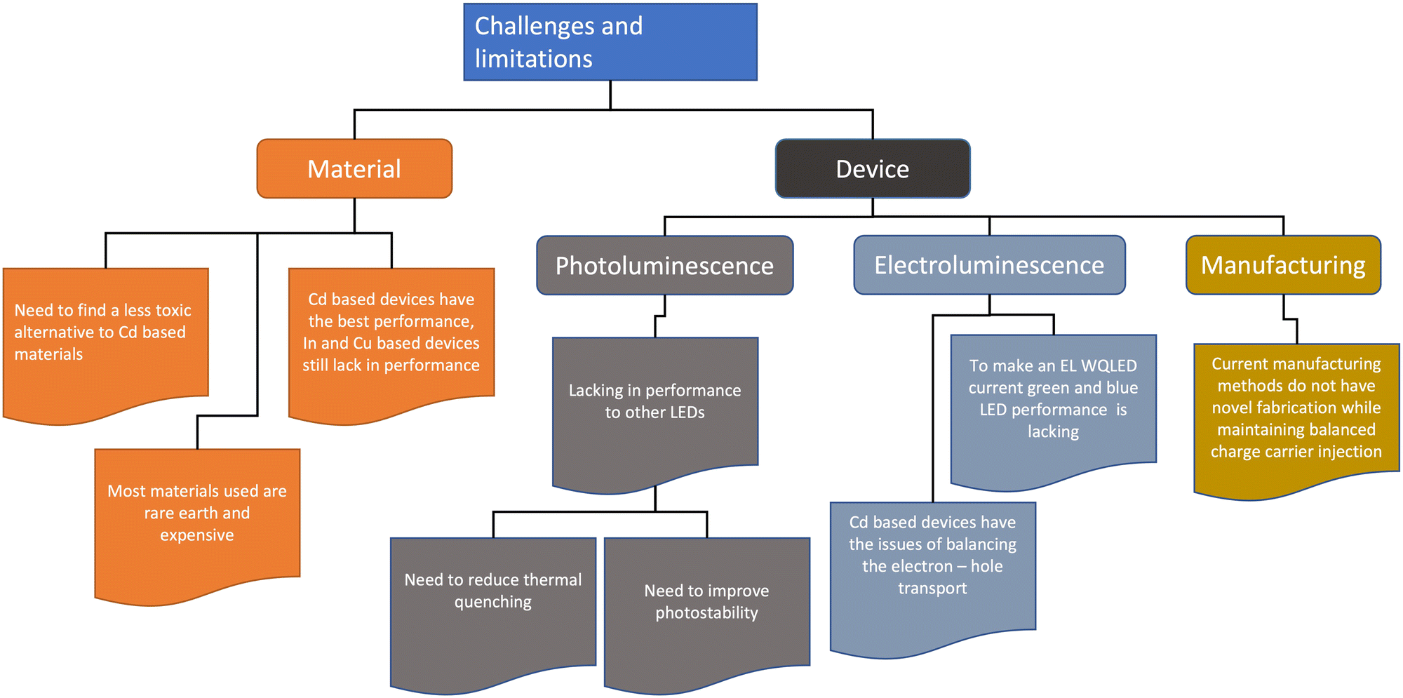 | ||
| Fig. 9 A summary of the challenges and limitations currently in QD lighting. | ||
Research has highlighted the other issues and limitations of QD, usually in the device fabrication phase. Since most quantum dot LED devices use a quaternary structure (Fig. 6b), the building of layers causes an exaggeration of the structural defects in not only the QD layer, but also the charge transport layers, which results in a surface tension gradient causing an inhomogeneous coating for the subsequent layers.86–89
Conclusions
QDs are especially suitable for light emission technologies (Fig. 1). This is mainly due to their characteristics of quantum confinement of electrons and holes, which enable photon emission with high luminescence/brightness, large tunability and narrow bandwidth. They have enhanced luminescence properties and lower power consumption than other materials. Nevertheless, there is still scope for improvements, particularly the integration of QDs into current architectures of optoelectronic devices and displays and their production methods. Even with these limitations, QDs are beginning to be adopted for next generation light-emitting devices, such as LEDs, displays and lighting. As shown in Fig. 10, since QDs can be synthesised ex situ in solution, they can be deposited on virtually any substrate using many different pre-existing printing and coating methods. This enables QLEDs to be fabricated over varying physical scales for both the consumer and industrial applications ranging from lighting fixtures, signs (with very large surface areas) to textiles.90–96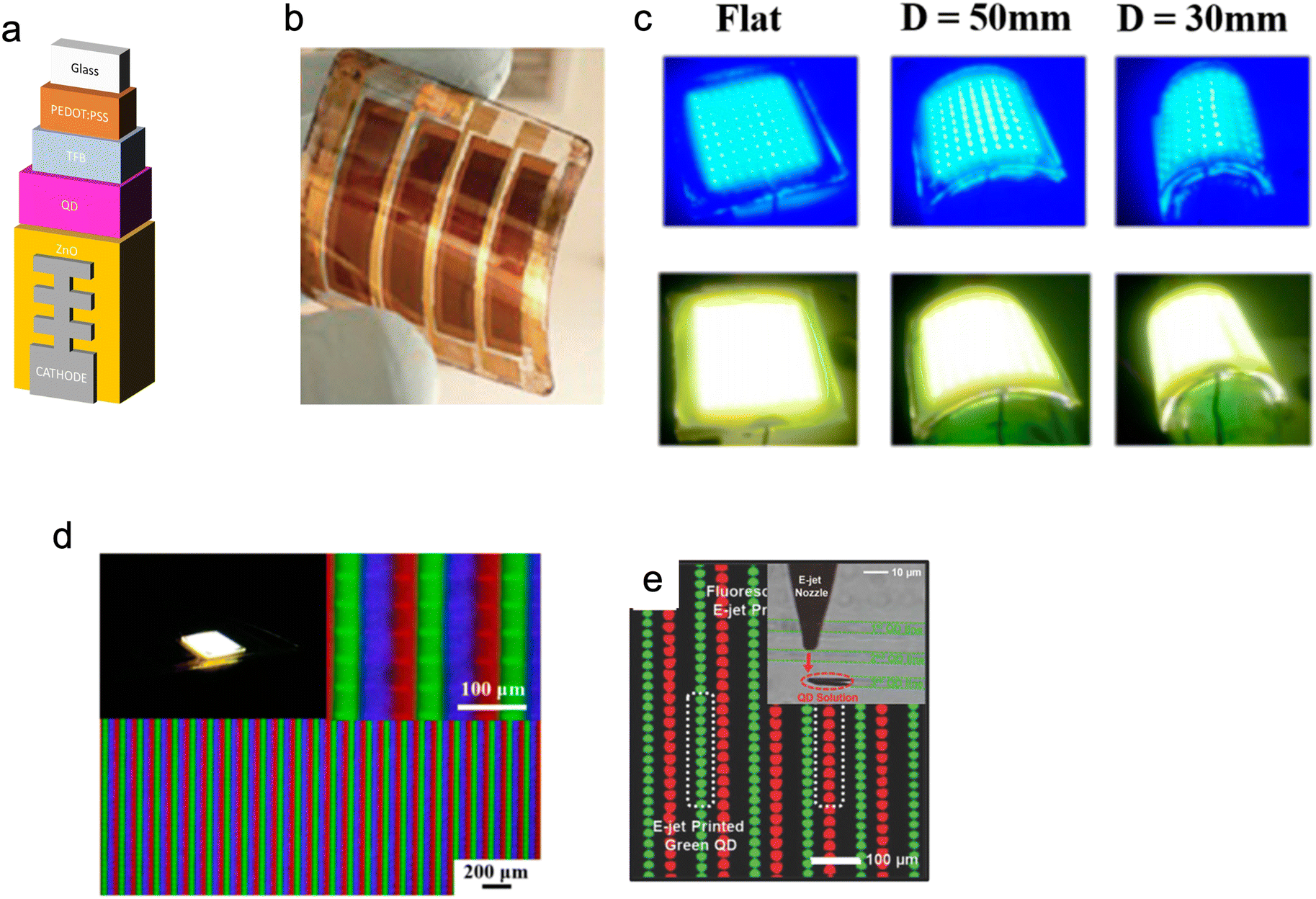 | ||
| Fig. 10 (a) Images of a device structure for fibre QLED. (b) Reproduced with permission.47 Copyright 2016 Author(s)) and (c) Pictures of QLEDS showing flexibility of the created devices and their performance at different levels of stress. (d) Image of QLEDs at different magnification levels. Reproduced with permission.97 Copyright 2020 by the authors. Licensee MDPI (e) composite fluorescence images of dual colour QD patterns formed by electro substrate during e-jet printing. Reproduced with permission.108 Copyright 2015, American Chemical Society. | ||
As shown in Fig. 11, to achieve QD white lighting (WQLEDs), there are currently two main approaches. The most widely used approach is to combine converted blue light from a GaN LED with photoluminescent green and red light from QDs to generate white emission; this method is known as phosphor-converted WQLEDs (pc-WQLEDs). Areas of development for this work focus on conversion materials to devices, with a large focus on the applications of the perovskite QD materials.97–101 The second way of making WQLEDs, which holds more promise for future development, is via white EL emission obtained through the electroluminescent action of combined blue, green and red QDs.53,78,102,103 Another interesting avenue of research is the use of QDs in communication technologies. QLEDs and QD lasers have shown improvement upon existing light-emitting devices, however, using QDs in visible light communication has not yet produced devices comparable to current radiofrequency methods.13,29,104
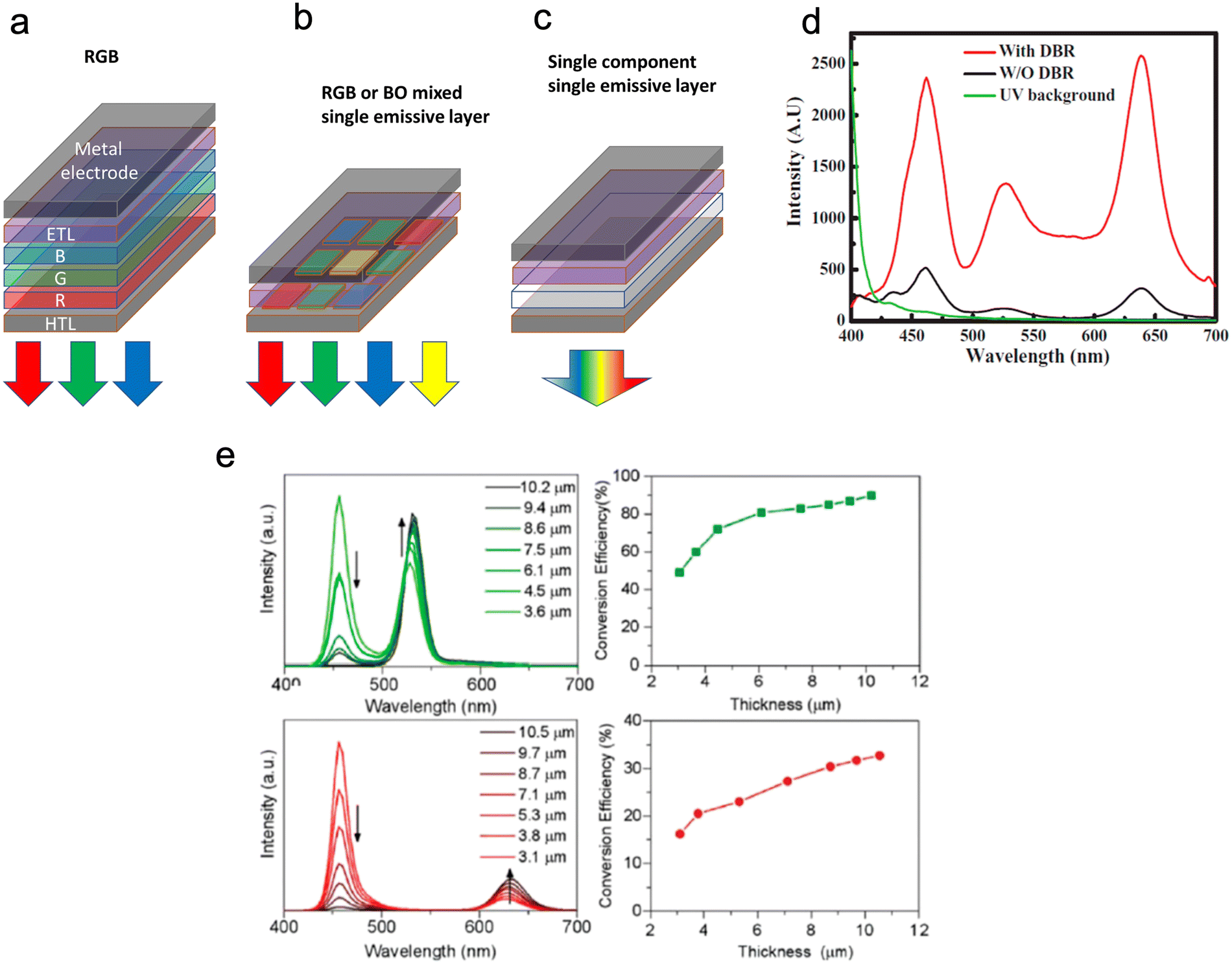 | ||
| Fig. 11 (a–c) show emitters and device structures in WLEDs. Device structures of WLEDs based on (a) GaN-LED, (b + c) ROGB (red, orange, green, blue) organic molecules/QDs, and (c) broad-spectrum emitting materials (d) Shows the EL spectra with and without a DBR structure. (e) shows PL spectra and light conversion efficiency (LCE) of green and red QD layers at different thicknesses. Reproduced with permission.97 Copyright 2020 by the authors. Licensee MDPI. | ||
Current commercially available QDs displays are limited to the photo-emissive type (Fig. 11). Photo-emissive displays use QDs to replace the traditional coloured phosphors, whereas electro-emissive displays work by using only QD LEDs. Even though photo emissive QD displays are commercially available, there are still drawbacks to these devices. These drawbacks include, off-angle viewing (due to the emitted light being focused straight outward from the screen) and the ability to achieve true black colour as the exciting backlight cannot be completely blocked.105 This can be overcome in electrically driven QD LEDs. Electro-emissive displays are still only available in labs as only the red and green QDs have the necessary features to act as electroluminescent subpixels. In contrast, blue QDs still need to be developed to produce the desired quantum efficiency and stability. The overall issues with the micro-LED display are that they remain bulkier, more expensive, and have lower resolutions per inch than any other display technology. Therefore, research on QDs used in displays includes shrinking the size of micro-LED pixels and eliminating the need for different-coloured LEDs in lighting by having combined white light QD pixels. These WQLEDs are brighter than existing screens and can produce black levels and colour accuracy to match OLED TVs.
Conflicts of interest
There are no conflicts to declare.Acknowledgements
J. M. Kim and G. A. J. Amaratunga gratefully acknowledges the funding from the Engineering and Physical Sciences Research Council (EPSRC, EP/P027628/1). A. R. C. Osypiw, B. Hou, S. Leoni and P. M. Smowton acknowledge the studentship funding from the Engineering and Physical Sciences Research Council (EPSRC, EP/T517951/1, 2579178). B. Hou acknowledges the financial support from the Cardiff University, Engineering and Physical Sciences Research Council (EPSRC, EP/V039717/1) and Royal Society of Chemistry (E21-9668828170) and B. Hou would also like to thank Dr David Westwood for illuminating discussions.Notes and references
- S.-Y. Cho, N. Oh, S. Nam, Y. Jiang and M. Shim, Enhanced device lifetime of double-heterojunction nanorod light-emitting diodes, Nanoscale, 2017, 9(18), 6103–6110 RSC.
- X. Mei, D. Jia, J. Chen, S. Zheng and X. Zhang, Approaching high-performance light-emitting devices upon perovskite quantum dots: Advances and prospects, Nano Today, 2022, 43, 101449 CrossRef CAS.
- T. Maxwell, M. G. Nogueira Campos, S. Smith, M. Doomra, Z. Thwin and S. Santra, Quantum Dots. Nanoparticles for Biomedical Applications, 2020, pp. 243–65 Search PubMed.
- L. Protesescu, S. Yakunin, M. I. Bodnarchuk, F. Krieg, R. Caputo and C. H. Hendon, et al., Nanocrystals of cesium lead halide perovskites (CsPbX3, X= Cl, Br, and I): novel optoelectronic materials showing bright emission with wide color gamut, Nano Lett., 2015, 15(6), 3692–3696 CrossRef CAS PubMed.
- S. M. Reimann and M. Manninen, Electronic structure of quantum dots, Rev. Mod. Phys., 2002, 74(4), 1283 CrossRef CAS.
- H. Kudilatt, B. Hou and M. E. Welland, Quantum Dots Microstructural Metrology: From Time-Resolved Spectroscopy to Spatially Resolved Electron Microscopy, Part. Part. Syst. Charact., 2020, 37(12), 2000192 CrossRef CAS.
- B. Hou, D. Parker, G. P. Kissling, J. A. Jones, D. Cherns and D. J. Fermín, Structure and band edge energy of highly luminescent CdSe1−xTex alloyed quantum dots, J. Phys. Chem. C, 2013, 117(13), 6814–6820 CrossRef CAS.
- G. Xu, S. Zeng, B. Zhang, M. T. Swihart, K. T. Yong and P. N. Prasad, New Generation Cadmium-Free Quantum Dots for Biophotonics and Nanomedicine, Chem. Rev., 2016, 116(19), 12234–12327 CrossRef CAS PubMed.
- H. Zang, H. Li, N. S. Makarov, K. A. Velizhanin, K. Wu and Y. S. Park, et al., Thick-Shell CuInS2/ZnS Quantum Dots with Suppressed “Blinking” and Narrow Single-Particle Emission Line Widths, Nano Lett., 2017, 17(3), 1787–1795 CrossRef CAS PubMed.
- F. Grillot, J. Duan, B. Dong and H. Huang, Uncovering recent progress in nanostructured light-emitters for information and communication technologies, Light: Sci. Appl., 2021, 10(1), 156 CrossRef CAS PubMed.
- D. Benito-Alifonso, S. Tremel, B. Hou, H. Lockyear, J. Mantell and D. J. Fermin, et al., Lactose as a “trojan horse” for quantum dot cell transport, Angew. Chem., Int. Ed., 2014, 53(3), 810–814 CrossRef CAS PubMed.
- O. Stroyuk, A. Raevskaya, F. Spranger, O. Selyshchev, V. Dzhagan and S. Schulze, et al., Origin and Dynamics of Highly Efficient Broadband Photoluminescence of Aqueous Glutathione-Capped Size-Selected Ag–In–S Quantum Dots, J. Phys. Chem. C, 2018, 122(25), 13648–13658 CrossRef CAS.
- A. Ren, H. Wang, W. Zhang, J. Wu, Z. Wang and R. V. Penty, et al., Emerging light-emitting diodes for next-generation data communications, Nat. Electron., 2021, 4(8), 559–572 CrossRef.
- K.-L. Wong, J.-C. G. Bünzli and P. A. Tanner, Quantum yield and brightness, J. Lumin., 2020, 224, 117256 CrossRef CAS.
- F. W. Eagle, N. Park, M. Cash and B. M. Cossairt, Surface Chemistry and Quantum Dot Luminescence: Shell Growth, Atomistic Modification, and Beyond, ACS Energy Lett., 2021, 6(3), 977–984 CrossRef CAS.
- P. T. Chin, C. de Mello Donegá, S. S. van Bavel, S. C. Meskers, N. A. Sommerdijk and R. A. Janssen, Highly luminescent CdTe/CdSe colloidal heteronanocrystals with temperature-dependent emission color, J. Am. Chem. Soc., 2007, 129(48), 14880–14886 CrossRef CAS PubMed.
- E. Jang, S. Jun, H. Jang, J. Lim, B. Kim and Y. Kim, White-light-emitting diodes with quantum dot color converters for display backlights, Adv. Mater., 2010, 22(28), 3076–3080 CrossRef CAS PubMed.
- P. Jing, J. Zheng, M. Ikezawa, X. Liu, S. Lv and X. Kong, et al., Temperature-dependent photoluminescence of CdSe-core CdS/CdZnS/ZnS-multishell quantum dots, J. Phys. Chem. C, 2009, 113(31), 13545–13550 CrossRef CAS.
- Y. Yin and A. P. Alivisatos, Colloidal nanocrystal synthesis and the organic–inorganic interface, Nature, 2005, 437(7059), 664–670 CrossRef CAS PubMed.
- J. Q. Grim, L. Manna and I. Moreels, A sustainable future for photonic colloidal nanocrystals, Chem. Soc. Rev., 2015, 44(16), 5897–5914 RSC.
- Y. Cao, B. Zhang, X. Tian, M. Gu and Y. Chen, Direct covalent modification of black phosphorus quantum dots with conjugated polymers for information storage, Nanoscale, 2019, 11(8), 3527–3533 RSC.
- E. Georgitzikis, P. E. Malinowski, Y. Li, J. Maes, L. M. Hagelsieb and S. Guerrieri, et al., Integration of PbS Quantum Dot Photodiodes on Silicon for NIR Imaging, IEEE Sens. J., 2020, 20(13), 6841–6848 CAS.
- R. Muñoz, E. M. Santos, C. A. Galan-Vidal, J. M. Miranda, A. Lopez-Santamarina and J. A. Rodriguez, Ternary Quantum Dots in Chemical Analysis. Synthesis and Detection Mechanisms, Molecules, 2021, 26(9), 2764 CrossRef PubMed.
- S. Jun, E. Jang, J. Park and J. Kim, Photopatterned semiconductor nanocrystals and their electroluminescence from hybrid light-emitting devices, Langmuir, 2006, 22(6), 2407–2410 CrossRef CAS PubMed.
- S. Goossens, G. Navickaite, C. Monasterio, S. Gupta, J. J. Piqueras and R. Pérez, et al., Broadband image sensor array based on graphene–CMOS integration, Nat. Photonics, 2017, 11(6), 366–371 CrossRef CAS.
- T.-H. Kim, K.-S. Cho, E. K. Lee, S. J. Lee, J. Chae and J. W. Kim, et al., Full-colour quantum dot displays fabricated by transfer printing, Nat. Photonics, 2011, 5(3), 176–182 CrossRef CAS.
- J. Callan and F. M. Raymo, Quantum dot sensors: technology and commercial applications, CRC Press, 2013 Search PubMed.
- J. Pan, A. A. O. El-Ballouli, L. Rollny, O. Voznyy, V. M. Burlakov and A. Goriely, et al., Automated synthesis of photovoltaic-quality colloidal quantum dots using separate nucleation and growth stages, ACS Nano, 2013, 7(11), 10158–10166 CrossRef CAS PubMed.
- Q. Shan, C. Wei, Y. Jiang, J. Song, Y. Zou and L. Xu, et al., Perovskite light-emitting/detecting bifunctional fibres for wearable LiFi communication, Light: Sci. Appl., 2020, 9, 163 CrossRef CAS PubMed.
- T. Lee, B. J. Kim, H. Lee, D. Hahm, W. K. Bae and J. Lim, et al., Bright and Stable Quantum Dot Light-Emitting Diodes, Adv. Mater., 2021, e2106276 Search PubMed.
- B. Hou, M. Sohn, Y.-W. Lee, J. Zhang, J. I. Sohn and H. Kim, et al., Chemically encoded self-organized quantum chain supracrystals with exceptional charge and ion transport properties, Nano Energy, 2019, 62, 764–771 CrossRef CAS.
- N. Laurand, B. Guilhabert, J. Mckendry, A. Kelly, B. Rae and D. Massoubre, et al., Colloidal quantum dot nanocomposites for visible wavelength conversion of modulated optical signals, Opt. Mater. Express, 2012, 2(3), 250–260 CrossRef CAS.
- B. Li, B. Hou and G. A. J. Amaratunga, Indoor photovoltaics, The Next Big Trend in solution-processed solar cells, InfoMat, 2021, 3(5), 445–459 CrossRef CAS.
- D. C. J. Neo, W. P. Goh, H. H. Lau, J. Shanmugam and Y. F. Chen, CuInS2 Quantum Dots with Thick ZnSexS1–x Shells for a Luminescent Solar Concentrator, ACS Appl. Nano Mater., 2020, 3(7), 6489–6496 CrossRef CAS.
- P. U. Alves, N. Laurand and M. D. Dawson, editors, Multicolor laser oscillation in a single self-assembled colloidal quantum dot microsphere, 2020 IEEE Photonics Conference (IPC), 2020, IEEE.
- B. Guilhabert, J. Herrnsdorf, Y. Gao, E. Mutlugun, H. Demir, N. Laurand, et al., editors, CdSe/ZnS colloidal quantum dots for solution-processed DFB lasers, 2013 IEEE Photonics Conference, 2013, IEEE.
- B. Guilhabert, C. Foucher, L. McLellan, A.-M. Haughey, Y. Gao, J. Herrnsdorf, et al., editors, Advances in colloidal quantum dot distributed feedback lasers hybridized on glass membranes, 2014 IEEE Photonics Conference, 2014, IEEE.
- D. Yan, M. Liu, Z. Li and B. Hou, Colloidal quantum dots and metal halide perovskite hybridization for solar cell stability and performance enhancement, J. Mater. Chem. A, 2021, 9(28), 15522–15541 RSC.
- V. M. Goossens, N. V. Sukharevska, D. N. Dirin, M. V. Kovalenko and M. A. Loi, Scalable fabrication of efficient pn junction lead sulfide quantum dot solar cells, Cell Rep. Phys. Sci., 2021, 100655 CrossRef CAS.
- G. H. Carey, A. L. Abdelhady, Z. Ning, S. M. Thon, O. M. Bakr and E. H. Sargent, Colloidal quantum dot solar cells, Chem. Rev., 2015, 115(23), 12732–12763 CrossRef CAS PubMed.
- B. Hou, B. S. Kim, H. K. H. Lee, Y. Cho, P. Giraud and M. Liu, et al., Multiphoton absorption stimulated metal chalcogenide quantum dot solar cells under ambient and concentrated irradiance, Adv. Funct. Mater., 2020, 30(39), 2004563 CrossRef CAS.
- C. R. Kagan, E. Lifshitz, E. H. Sargent and D. V. Talapin, Building devices from colloidal quantum dots, Science, 2016, 353(6302), aac5523 CrossRef PubMed.
- J. Mei, N. L. Leung, R. T. Kwok, J. W. Lam and B. Z. Tang, Aggregation-Induced Emission: Together We Shine, United We Soar!, Chem. Rev., 2015, 115(21), 11718–11940 CrossRef CAS PubMed.
- F. Antolini and L. Orazi, Quantum Dots Synthesis Through Direct Laser Patterning: A Review, Front Chem, 2019, 7, 252 CrossRef CAS PubMed.
- H. Lee, W. Harden-Chaters, S. D. Han, S. Zhan, B. Li and S. Y. Bang, et al., Nano-to-microporous networks via inkjet printing of ZnO nanoparticles/graphene hybrid for ultraviolet photodetectors, ACS Appl. Nano Mater., 2020, 3(5), 4454–4464 CrossRef CAS.
- B. Dou, J. B. Whitaker, K. Bruening, D. T. Moore, L. M. Wheeler and J. Ryter, et al., Roll-to-roll printing of perovskite solar cells, ACS Energy Lett., 2018, 3(10), 2558–2565 CrossRef CAS.
- M. Liu, N. Yazdani, M. Yarema, M. Jansen, V. Wood and E. H. Sargent, Colloidal quantum dot electronics, Nat. Electron., 2021, 4(8), 548–558 CrossRef.
- J. Y. Kim, O. Voznyy, D. Zhitomirsky and E. H. Sargent, 25th anniversary article: Colloidal quantum dot materials and devices: a quarter-century of advances, Adv. Mater., 2013, 25(36), 4986–5010 CrossRef CAS PubMed.
- Y. Deng, F. Peng, Y. Lu, X. Zhu, W. Jin and J. Qiu, et al., Solution-processed green and blue quantum-dot light-emitting diodes with eliminated charge leakage, Nat. Photonics, 2022, 1–7 Search PubMed.
- F. Zhang, Z. Ma, Z. Shi, X. Chen, D. Wu and X. Li, et al., Recent advances and opportunities of lead-free perovskite nanocrystal for optoelectronic application, Energy Mater. Adv., 2021, 5198145 CAS.
- H. Lee and Y. T. Chun, Supporting Information Fibertronic Quantum-Dot Light-Emitting Diode for E-Textile, ACS Appl. Nano Mater., 2020, 3, 11060–11069 CrossRef CAS.
- H. Lee and Y. T. Chun, Fibertronic Quantum-Dot Light-Emitting Diode for E-Textile, ACS Appl. Nano Mater., 2020, 3(11), 11060–11069 CrossRef CAS.
- B. Li, M. Lu, J. Feng, J. Zhang, P. M. Smowton and J. I. Sohn, et al., Colloidal quantum dot hybrids: an emerging class of materials for ambient lighting, J. Mater. Chem. C, 2020, 8(31), 10676–10695 RSC.
- H. Zhang, Q. Su and S. Chen, Quantum-dot and organic hybrid tandem light-emitting diodes with multi-functionality of full-color-tunability and white-light-emission, Nat. Commun., 2020, 11(1), 2826 CrossRef CAS PubMed.
- H. Xiang, R. Wang, J. Chen, F. Li and H. Zeng, Research progress of full electroluminescent white light-emitting diodes based on a single emissive layer, Light: Sci. Appl., 2021, 10(1), 206 CrossRef CAS PubMed.
- X. Chen, W.-G. Lu, J. Tang, Y. Zhang, Y. Wang and G. D. Scholes, et al., Solution-processed inorganic perovskite crystals as achromatic quarter-wave plates, Nat. Photonics, 2021, 15(11), 813–816 CrossRef.
- X. Chen, F. Zhang, Y. Ge, L. Shi, S. Huang and J. Tang, et al., Centimeter-Sized Cs4 PbBr6 Crystals with Embedded CsPbBr3 Nanocrystals Showing Superior Photoluminescence: Nonstoichiometry Induced Transformation and Light-Emitting Applications, Adv. Funct. Mater., 2018, 28, 1706567 CrossRef.
- S. N. R. Kantareddy, I. Mathews, S. Sun, M. Layurova, J. Thapa and J.-P. Correa-Baena, et al., Perovskite PV-Powered RFID: Enabling Low-Cost Self-Powered IoT Sensors, IEEE Sens. J., 2020, 20(1), 471–478 CAS.
- D. Pan, Y. Fu, N. Spitha, Y. Zhao, C. R. Roy and D. J. Morrow, et al., Deterministic, Nat. Nanotechnol., 2020, 16(2), 159–165 CrossRef PubMed.
- D. Vila-Liarte, M. W. Feil, A. Manzi, J. L. Garcia-Pomar, H. Huang and M. Doblinger, et al., Templated-Assembly of CsPbBr3 Perovskite Nanocrystals into 2D Photonic Supercrystals with Amplified Spontaneous Emission, Angew. Chem., Int. Ed., 2020, 59(40), 17750–17756 CrossRef CAS PubMed.
- W. Zhan, L. Meng, C. Shao, X.-G. Wu, K. Shi and H. Zhong, In Situ Patterning Perovskite Quantum Dots by Direct Laser Writing Fabrication, ACS Photonics, 2021, 8(3), 765–770 CrossRef CAS.
- S.-M. Jung, T. H. Lee, S. Y. Bang, S. D. Han, D.-W. Shin and S. Lee, et al., Modelling charge transport and electro-optical characteristics of quantum dot light-emitting diodes, npj Comput. Mater., 2021, 7(1), 1–11 CrossRef.
- H. W. Choi, D.-W. Shin, J. Yang, S. Lee, C. Figueiredo and S. Sinopoli, et al., Smart textile lighting/display system with multifunctional fibre devices for large scale smart home and IoT applications, Nat. Commun., 2022, 13(1), 1–9 Search PubMed.
- S. G. Solomon and P. Lennie, The machinery of colour vision, Nat. Rev. Neurosci., 2007, 8(4), 276–286 CrossRef CAS PubMed.
- T. Young, II. The Bakerian Lecture. On the theory of light and colours, Philos. Trans. R. Soc. London, 1802, 92, 12–48 CrossRef.
- C. T. B. Samarakoon, Perception-Aware Optimisation Methodologies for Quantum Dot Based Displays and Lighting, PhD thesis, University of Cambridge, 2021 Search PubMed.
- Y. Shirasaki, G. J. Supran, M. G. Bawendi and V. Bulović, Emergence of colloidal quantum-dot light-emitting technologies, Nat. Photonics, 2013, 7(1), 13–23 CrossRef CAS.
- E. F. Schubert, Light-emitting diodes: E. Fred Schubert, 2018 Search PubMed.
- H. J. Round, A note on carborundum. Semiconductor Devices: Pioneering Papers, World Scientific, 1991, p. 879 Search PubMed.
- C. Weisbuch, Historical perspective on the physics of artificial lighting, C. R. Phys., 2018, 19(3), 89–112 CrossRef CAS.
- N. Zheludev, The life and times of the LED—a 100-year history, Nat. Photonics, 2007, 1(4), 189–192 CrossRef CAS.
- O. Lossev, CII. Luminous carborundum detector and detection effect and oscillations with crystals, London, Edinburgh Dublin Philos. Mag. J. Sci., 1928, 6(39), 1024–1044 CrossRef CAS.
- J. Owen and L. Brus, Chemical Synthesis and Luminescence Applications of Colloidal Semiconductor Quantum Dots, J. Am. Chem. Soc., 2017, 139(32), 10939–10943 CrossRef CAS PubMed.
- V. Wood and V. Bulović, Colloidal quantum dot light-emitting devices, Nano Rev., 2010, 1(1), 5202 CrossRef PubMed.
- C. Jiang, J. Zou, Y. Liu, C. Song, Z. He and Z. Zhong, et al., Fully solution-processed tandem white quantum-dot light-emitting diode with an external quantum efficiency exceeding 25%, ACS Nano, 2018, 12(6), 6040–6049 CrossRef CAS PubMed.
- S. Tamang, C. Lincheneau, Y. Hermans, S. Jeong and P. Reiss, Chemistry of InP nanocrystal syntheses, Chem. Mater., 2016, 28(8), 2491–2506 CrossRef CAS.
- M. D. Tessier, D. Dupont, K. De Nolf, J. De Roo and Z. Hens, Economic and Size-Tunable Synthesis of InP/ZnE (E = S, Se) Colloidal Quantum Dots, Chem. Mater., 2015, 27(13), 4893–4898 CrossRef CAS.
- S.-B. Cho, J. I. Sohn, S.-S. Lee, S.-G. Moon, B. Hou and I.-K. Park, Colour-encoded electroluminescent white light-emitting diodes enabled using perovskite–Cu–In–S quantum composites, J. Mater. Chem. C, 2021, 9(22), 7027–7034 RSC.
- Y. H. Won, O. Cho, T. Kim, D. Y. Chung, T. Kim and H. Chung, et al., Highly efficient and stable InP/ZnSe/ZnS quantum dot light-emitting diodes, Nature, 2019, 575(7784), 634–638 CrossRef CAS PubMed.
- D. W. Shin, Y. H. Suh, S. Lee, B. Hou, S. D. Han and Y. Cho, et al., Waterproof Flexible InP@ ZnSeS Quantum Dot Light-Emitting Diode, Adv. Opt. Mater., 2020, 8(6), 1901362 CrossRef CAS.
- S. Y. Bang, Y.-H. Suh, X.-B. Fan, D.-W. Shin, S. Lee and H. W. Choi, et al., Technology progress on quantum dot light-emitting diodes for next-generation displays, Nanoscale Horiz., 2021, 6(2), 68–77 RSC.
- M. Cinquino, C. T. Prontera, M. Pugliese, R. Giannuzzi, D. Taurino and G. Gigli, et al., Light-Emitting Textiles: Device Architectures, Working Principles, and Applications, Micromachines, 2021, 12(6), 652 CrossRef PubMed.
- K. Yoshida, P. P. Manousiadis, R. Bian, Z. Chen, C. Murawski and M. C. Gather, et al., 245 MHz bandwidth organic light-emitting diodes used in a gigabit optical wireless data link, Nat. Commun., 2020, 11(1), 1171 CrossRef CAS PubMed.
- S. Yang, C. Bi and J. Tian, Highly Pure White Light-Emitting Single-Component Perovskite Colloidal Quantum Dots. The, J. Phys. Chem. C, 2021, 125(34), 18810–18816 CrossRef CAS.
- Y. H. Suh, S. Lee, S. M. Jung, S. Y. Bang, J. Yang and X. B. Fan, et al., Engineering Core Size of InP Quantum Dot with Incipient ZnS for Blue Emission, Adv. Opt. Mater., 2022, 2102372 CrossRef CAS.
- H. Liu, K. Rong, Z. Li and J. Chen, Experimental demonstration of nanophotonic devices and circuits with colloidal quantum dot waveguides, Opt. Express, 2020, 28(16), 23091–23104 CrossRef CAS PubMed.
- K. Rong, H. Liu, K. Shi and J. Chen, Pattern-assisted stacking colloidal quantum dots for photonic integrated circuits, Nanoscale, 2019, 11(29), 13885–13893 RSC.
- K.-S. Cho, E. K. Lee, W.-J. Joo, E. Jang, T.-H. Kim and S. J. Lee, et al., High-performance crosslinked colloidal quantum-dot light-emitting diodes, Nat. Photonics, 2009, 3(6), 341–345 CrossRef CAS.
- T.-H. Kim, D.-Y. Chung, J. Ku, I. Song, S. Sul and D.-H. Kim, et al., Heterogeneous stacking of nanodot monolayers by dry pick-and-place transfer and its applications in quantum dot light-emitting diodes, Nat. Commun., 2013, 4(1), 1–12 Search PubMed.
- F. Fan, O. Voznyy, R. P. Sabatini, K. T. Bicanic, M. M. Adachi and J. R. McBride, et al., Continuous-wave lasing in colloidal quantum dot solids enabled by facet-selective epitaxy, Nature, 2017, 544(7648), 75–79 CrossRef CAS PubMed.
- C. Foucher, B. Guilhabert, N. Laurand and M. D. Dawson, Wavelength-tunable colloidal quantum dot laser on ultra-thin flexible glass, Appl. Phys. Lett., 2014, 104, 141108 CrossRef.
- C. Foucher, I. D. W. Samuel, G. Faulkner, D. C. O'Brien, H. Haas and N. Laurand, et al., Flexible Glass Hybridized Colloidal Quantum Dots for Gb/s Visible Light Communications, IEEE Photon. J., 2018, 10(1), 1–11 Search PubMed.
- S. Choi, W. Jo, Y. Jeon, S. Kwon, J. H. Kwon and Y. H. Son, et al., Multi-directionally wrinkle-able textile OLEDs for clothing-type displays, npj Flexible Electron., 2020, 4(1), 1–9 CrossRef.
- H. Zhang and J. A. Rogers, Recent Advances in Flexible Inorganic Light Emitting Diodes: From Materials Design to Integrated Optoelectronic Platforms, Adv. Opt. Mater., 2019, 7, 1800936 CrossRef.
- J.-S. Park, J. Kyhm, H. H. Kim, S. Jeong, J. Kang and S.-E. Lee, et al., Alternative patterning process for realization of large-area, full-color, active quantum dot display, Nano Lett., 2016, 16(11), 6946–6953 CrossRef CAS PubMed.
- Y. Wang, I. Fedin, H. Zhang and D. V. Talapin, Direct optical lithography of functional inorganic nanomaterials, Science, 2017, 357(6349), 385–388 CrossRef CAS PubMed.
- S. Nizamoglu, T. Ozel, E. Sari and H. V. Demir, White light generation using CdSe/ZnS core–shell nanocrystals hybridized with InGaN/GaN light emitting diodes, Nanotechnology, 2007, 18(6), 065709 CrossRef.
- J. McKittrick and L. E. Shea-Rohwer, Down conversion materials for solid-state lighting, J. Am. Ceram. Soc., 2014, 97(5), 1327–1352 CrossRef CAS.
- T. Guner and M. M. Demir, A review on halide perovskites as color conversion layers in white light emitting diode applications, Phys. Status Solidi A, 2018, 215(13), 1800120 CrossRef.
- Y. Wei, Z. Cheng and J. Lin, An overview on enhancing the stability of lead halide perovskite quantum dots and their applications in phosphor-converted LEDs, Chem. Soc. Rev., 2019, 48(1), 310–350 RSC.
- S. Nizamoglu, G. Zengin and H. V. Demir, Color-converting combinations of nanocrystal emitters for warm-white light generation with high color rendering index, Appl. Phys. Lett., 2008, 92(3), 031102 CrossRef.
- Y. Cho, S. Pak, B. Li, B. Hou and S. Cha, Enhanced Direct White Light Emission Efficiency in Quantum Dot Light-Emitting Diodes via Embedded Ferroelectric Islands Structure, Adv. Funct. Mater., 2021, 31(41), 2104239 CrossRef CAS.
- S. Y. Bang, X. B. Fan, S. M. Jung, J. Yang, D. W. Shin and Y. H. Suh, et al., Highly stable and scalable blue QD-LED via an evaporated TiO2 thin film as an electron transport layer, Adv. Opt. Mater., 2020, 8(21), 2001172 CrossRef CAS.
- C. Bao, W. Xu, J. Yang, S. Bai, P. Teng and Y. Yang, et al., Bidirectional optical signal transmission between two identical devices using perovskite diodes, Nat. Electron., 2020, 3(3), 156–164 CrossRef PubMed.
- Y. Nakanishi, T. Takeshita, Y. Qu, H. Imabayashi, S. Okamoto and H. Utsumi, et al., Active matrix QD-LED with top emission structure by UV lithography for RGB patterning, J. Soc. Inf. Disp., 2020, 28(6), 499–508 CrossRef CAS.
| This journal is © The Royal Society of Chemistry 2022 |