
 Open Access Article
 This Open Access Article is licensed under a
 Creative Commons Attribution 3.0 Unported Licence
Dielectric properties correlation with microstructure in ABi4Ti4O15 (A = Sr, Ba) bismuth layered ferroelectrics
Vipul Kumar
Sharma
 a,
Rashi
Nathawat
a and
Satyapal S.
Rathore
*ab
a,
Rashi
Nathawat
a and
Satyapal S.
Rathore
*ab
aFunctional Ceramics and Smart Materials Lab, Department of Physics, Manipal University Jaipur, Jaipur, 303007, India. E-mail: satyapal03@gmail.com; Tel: +91-9930437849
bDepartment of Physics, Cluster University of Jammu, Jammu, Jammu & Kashmir, 180001, India
First published on 25th April 2022
Abstract
The bismuth layered ferroelectrics (BLFs) BaBi4Ti4O15 and SrBi4Ti4O15 were synthesized using solid-state-reaction technique and the impact of ‘thermal etching’ on their microstructure and dielectric and ferroelectric properties was thoroughly investigated. The phase formation and crystallization to the orthorhombic A21am phase was confirmed by XRD followed by Rietveld refinement. The thermally etched compounds depict the formation of highly uniform plate-like grain distribution with a reduced grain size. The effect of improved microstructure was also evident in the dielectric properties with a colossal change in the dielectric constant, ε′. Furthermore, the study suggests that the ferroelectric polarization can also be improved by thermal etching, reducing the contribution due to non-ferroelectric components. The impedance analysis using a brick-layer model shows that impedance is predominantly due to grains (bulk) with a relatively small contribution due to grain boundaries in these BLFs. The observed change in macroscopic properties was attributed to the modification in grain–grain boundary configuration post thermal etching.
1 Introduction
Piezoelectric devices have been an integral part of our technological evolution due to their extensive applications in consumer electronics, aerospace, defence, health monitoring, scientific equipment and many others.1–4 However, the majority of these devices utilize ceramic piezoelectrics, which in turn are predominantly Pb-based piezoelectric systems.5–11 The long term adverse impact of Pb on the human body and environment due to a lack of appropriate disposal has been raised by organizations such as the WHO and RoHS from time to time.12,13 Due to the utility of piezoelectric devices, the development of eco-friendly alternatives to Pb-based piezoelectric materials with comparable device performances can be considered one of the most urgent challenges faced by the scientific community. Thus, the search for Pb-free piezoelectric systems to develop clean and sustainable technology has seen an upsurge in the last decade.14,15 One of the promising piezoelectric systems to envisage Pb-free devices in the future is the Aurivillius family of compounds. The piezo-properties of these compounds were observed to be inferior when compared with their Pb-based counterparts. However, due to their high Curie temperature, large dielectric constant, low losses and excellent thermal and chemical stability they have emerged as potential candidates for high temperature piezo-electric applications. In addition, many compounds in these Pb-free ceramics also possess a relaxor ferroelectric state with a good piezo-response, which makes them an ideal system to be used over a temperature range as their dielectric constant remains maximum in a wide temperature window.16–21The Aurivillius family of compounds, also known as bismuth layered ferroelectrics (BLFs) is represented by [Bi2O2]2+ [Am−1BmO3m+1]2−. Here A is mono, di, or trivalent or their mixture, B is tetravalent, pentavalent or their mixture of elements, and m = 1, 2, 3, 4 or 5. Due to a large possible combination of A and B sites as well as m, many derivatives of BLFs have been reported in the literature.22 Interestingly, the piezo-properties of this system have shown significant dependence on the partial and complete substitution at the A, B and Bi sites. Moreover, ion substitution is one of the most common approaches to introduce new functionalities such as magnetic order in these complex oxides.23 Furthermore, the physical properties of these oxides were observed to show dependence on the synthesis conditions and processing parameters. Thus, the Pb-free Aurivillius family of compounds possesses excellent dielectric and piezoelectric properties, which can be tailored by controlling the synthesis conditions, processing parameters and ionic substitutions based on crystal chemical principles. Therefore, careful control of these parameters becomes essential to achieve the reproducibility of functional properties for any specific application.
In the present work, an attempt is made to understand the effect of one such processing parameter, thermal etching, on the structural, dielectric and piezo-electric properties of BaBi4Ti4O15 and SrBi4Ti4O15. These two isomorph complex oxides were chosen as they possess contrasting dielectric responses conforming to relaxor ferroelectric and normal ferroelectric phases respectively. Thus their dielectric properties cover a wide spectrum of bismuth layered ferroelectric systems. A highly uniform plate-like microstructure (typical of BLFs) was observed for both the phases post thermal etching, with a significant variation in dielectric and piezoelectric properties. To understand a correlation between the microstructure and macroscopic properties, a brick layer model has been proposed which could be utilized to understand the dielectric properties of the Aurivillius family of compounds in general.
2 Experimental details
The polycrystalline BaBi4Ti4O15 (BBT) and SrBi4Ti4O15 (SBT) were synthesized using a solid state reaction technique. Initially, highly pure BaCo3/SrCo3, Bi2O3 and TiO2 were ground in an agate mortar and pestle. The precursor mixture to synthesize BBT was calcined for 4 h at 800 °C followed by intermediate grinding of the powder and recalcination at 950 °C for 8 h. On the other hand, the initial precursor mixture to synthesize SBT was calcined at 900 °C for 3 h. The single phase powders of both materials were pressed into pellets of 10 mm in diameter and 2 mm thickness using polyvinyl alcohol (PVA) as the binder. The ‘green’ pellets of both materials were then sintered at 1100 °C for 2 h and named the ‘as-sintered’ (AS) pellet in the present work. These as-sintered pellets of both materials were mirror polished with Al2O3 abrasive of size 0.5 μm using BUEHLER polisher. These fine polished pellets were then heat treated at 1030 °C for 30 minutes in a high temperature furnace and called ‘thermally-etched’ (TE) pellets in the current study.The room temperature crystal structure study was performed using a Bruker D8 Advance X-ray diffractometer with Cu-Kα radiation of 1.54 Å. The microstructural study was performed with a JEOL make JSM-7610F Plus FESEM. The high temperature (RT to 923 K) dielectric measurements for the AS and TE pellets of both materials were performed at various frequencies (1 Hz to 10 MHz) using a Novocontrol, Concept – 80 broadband dielectric spectrometer. Furthermore, the P–E loop measurements were carried out with an AIXACCT P–E loop analyser.
3 X-ray diffraction studies
The room temperature powder X-ray diffraction patterns for BaBi4Ti4O15 and its isomorph SrBi4Ti4O15 are shown in Fig. 1(b) and (c) respectively. The Rietveld refinement reveals that both Aurivillius compounds crystallize in the orthorhombic (pseudo-tetragonal) phase conforming to a non-centrosymmetric A21am space group symmetry (Z = 2). Previous studies have shown a possibility of both BaBi4Ti4O15 and SrBi4Ti4O15 existing in tetragonal I4/mmm symmetry, due to nearly the same values of in plane (a–b) lattice parameters ‘a’ and ‘b’.24 The ratio of these lattice parameters was observed in the present study to be 1.0006 and 1.001 for BaBi4Ti4O15 and SrBi4Ti4O15 respectively. Due to similar values of ‘a’ and ‘b’, all the reflections in the powder X-ray diffraction pattern could also be associated with the centrosymmetric tetragonal structure. However, previous high-resolution synchrotron XRD and selected area electron diffraction studies revealed the presence of Bragg reflections which are forbidden by tetragonal symmetry25 and hence the existence of both Aurivillius compounds in an orthorhombic phase. | ||
| Fig. 1 (a) The crystal structure of BaBi4Ti4O15 viewed along the [001] direction (z = −0.25 to z = 0.75); for details please refer to the text. The Rietveld plot for (b) BaBi4Ti4O15 and (c) SrBi4Ti4O15 obtained by structure refinement in the orthorhombic space group A21am. The observed data, calculated pattern and difference plot are shown by the red circle, black line through a circle and blue line at the bottom respectively. The green vertical bars indicate the allowed Bragg reflections. | ||
Thus, in the current study, initially both A21am and I4/mmm symmetries were modelled for refinement, and both compounds show a slightly better value of χ2 for A21am. The calculated pseudo-tetragonal values  for BaBi4Ti4O15 and SrBi4Ti4O15 are 3.863 and 3.847 respectively, which are in good agreement with the literature.26 The Rietveld plot for both compounds shows the absence of any unaccounted diffraction peak; and all reflections could be indexed to an orthorhombic structure, indicating the synthesized ceramics are in the single phase. The structure refinement parameters are summarized in Table 1, and indicate a good fit between the observed and calculated pattern. The refinement demonstrates an expected decrease in all the dimensional lattice parameters, ‘a’, ‘b’, and ‘c’ of SBT, for relatively smaller Sr2+ ion substitution at the Ba2+ site. The result of this study is in good agreement with the literature.27
| Atom | Wyc. | x | y | z | Occup |
|---|---|---|---|---|---|
| Bi1 | 4a | 0.1186(7)[0.1313(5)] | 0.3852(3)[0.3786(7)] | 0.00000 | 0.50 |
| Ba1 [Sr1] | 4a | 0.1186(7)[0.1313(5)] | 0.3852(3)[0.3786(7)] | 0.00000 | 0.50 |
| Bi2 | 8b | 0.5403(7)[0.5415(1)] | 0.2306(5)[0.2756(1)] | 0.2248(2)[0.2239(9)] | 1.00 |
| Bi3 | 8b | 0.1765(8)[0.1569(7)] | 0.2855(4)[0.2812(4)] | 0.9008(5)[0.9005(8)] | 0.75 |
| Ba2 [Sr2] | 8b | 0.1765(8)[0.1569(7)] | 0.2855(4)[0.2812(4)] | 0.9008(5)[0.9005(8)] | 0.25 |
| Ti1 | 8b | 0.3553(1)[0.2852(5)] | 0.4730(4)[0.4474(5)] | 0.5709(7)[0.5752(4)] | 1.00 |
| Ti2 | 8b | 0.5462(7)[0.5421(5)] | −0.2780(6)[−0.267(1)] | 0.3449(6)[0.3456(4)] | 1.00 |
| O1 | 4a | 0.6030(8)[0.5703(2)] | 0.1951(9)[0.2107(4)] | 0.00000 | 1.00 |
| O2 | 8b | 0.2378(1)[0.2378(5)] | 0.3120(8)[0.3120(7)] | 0.4156(2)[0.4156(2)] | 1.00 |
| O3 | 8b | 0.3805(4)[0.3509(5)] | 0.0344(8)[−0.0018(2)] | 0.5564(2)[0.5511(3)] | 1.00 |
| O4 | 8b | 0.5463(5)[0.5613(2)] | 0.2733(4)[0.3398(3)] | 0.2684(9)[0.2755(8)] | 1.00 |
| O5 | 8b | 0.4174(3)[0.4174(2)] | 0.4672(2)[0.4672(7)] | 0.4486(8)[0.4486(6)] | 1.00 |
| O6 | 8b | 0.2220(3)[0.2220(3)] | 0.2448(6)[0.2448(7)] | 0.4148(6)[0.4148(7)] | 1.00 |
| O7 | 8b | 0.4053(7)[0.4332(7)] | 0.1238(2)[0.1524(1)] | 0.3440(8)[0.3452(5)] | 1.00 |
| O8 | 8b | 0.2577(4)[0.2495(3)] | 0.3258(9)[0.1817(6)] | 0.6514(5)[0.6511(3)] | 1.00 |
| BaBi4Ti4O15 | SrBi4Ti4O15 | ||||
| a | 5.4655(3) Å | 5.4445(3) Å | |||
| b | 5.4621(2) Å | 5.4371(2) Å | |||
| c | 41.788(5) Å | 40.911(3) Å | |||
| α = β = γ | 90° | 90° | |||
| Space group | A21am (39) | A21am (39) | |||
| χ 2, RP and RWP | 1.58, 14.1 and 16.3 | 1.43, 12.2 and 13.3 | |||
| 2θ, X-ray source | 10° to 100°, Cu Kα | 10° to 100°, Cu Kα |
The crystal structure of the bismuth-layered Aurivillius phase is shown in Fig. 1(a). A unit cell contains two formula units of BaBi4Ti4O15. The crystal structure can be best represented when viewed from [001]. From z = −0.25 to 0.75 it shows two units of BaBi4Ti4O15, indicated by the dotted two-headed arrow. This unit (z = 0.25 to 0.75) can be further divided into four (m = 4) perovskite-like units of (BaBi) TiO3, with the overall composition of BaBi2Ti4O13 (shown by the solid line). These perovskite-like units are sandwiched between Bi2O2 layers along the pseudo-tetragonal c-axis (designated as a solid double-sided arrow), giving it the characteristic name of bismuth layered structures. The 4a and 8b sites between the perovskite-like units are partially occupied by Bi and Ba, with site occupancy of 50% each (4a) and 75% and 25% (8b) respectively. The bismuth layered structure is attributed to the Bi2 (8b) site completely occupied by Bi3+ ions.
4 Microstructural analysis
The FESEM electron photo-micrographs for BBT and SBT sintered pellets are shown in Fig. 2. A non-uniform distribution of crystallites with the presence of small (∼0.1 μm) to large (∼2 μm) grains can be clearly seen for the as-sintered surfaces of BBT and SBT [Fig. 2(a and d)]. However, the thermally etched pellets of synthesized oxides [Fig. 2(b and e)] show a highly uniform grain distribution. This plate-like grain morphology is a characteristic of BLF orthorhombic phases. The histograms in Fig. 2(c) and (f) show a comparative grain size distribution over the captured image for BBT and SBT oxides respectively. The statistical average grain size for BBT-AS and BBT-TE is 0.5969 μm and 0.3604 μm respectively. However, the calculated average grain size for SBT-AS and SBT-TE was obtained as 1.0683 μm and 0.4114 μm respectively. This visible enhancement in grain morphology and reduction in average grain size of the TE pellet in both materials reveals that the thermal etching is a simple yet effective processing method to improve the microstructure of the Aurivillius family of compounds. However, the statistically calculated average grain size for SBT was observed to be greater than that for BBT, which indicates dependence on the A-site composition. This improvement in grain morphology can be attributed to redistribution of surface energy due to the diffusion of atoms from the grain boundary.28,29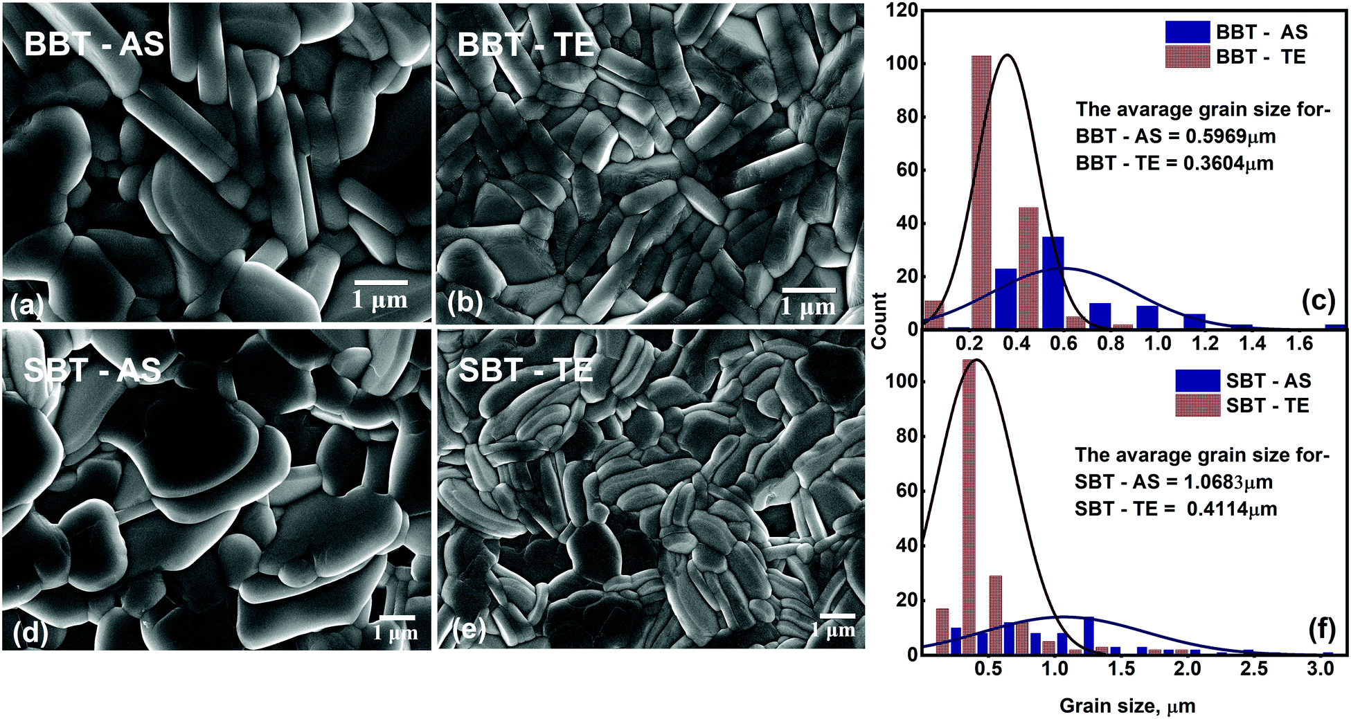 | ||
| Fig. 2 The scanning electron photomicrograph for (a) BBT-AS, (b) BBT-TE, (d) SBT-AS and (e) SBT-TE along with the statistical grain size distribution curve for (c) BBT and (f) SBT. The continuous grey and blue lines in the distribution curve represent the distribution over the histogram, and do not represent any mathematical relation. | ||
The fundamental theory of crystallization may give some insight to understanding the growth of the observed random plate-like grains in both materials.30 The BBT and SBT both have a bismuth layered structure with stacking of four perovskite-like units sandwiched between the layer of bismuth oxide (Bi2O2) [Fig. 1(a)] along the c-axis. This is the reason for the large value of lattice constant ‘c’ (7.5 times) when compared with ‘a’ and ‘b’. All the crystal unit cells assemble themselves along crystallographic axes during heat treatment and a large array of unit cells then forms a grain. The layered axis was observed to be the hard growing direction whereas a and b are relatively easy growing axes.31 This results in the observed typical pellet-like grains with a very small breadth (c-axis) compared to its length (a and b axes).
5 Dielectric studies
The temperature-dependent (30 °C to 700 °C) dielectric response (real part of the dielectric constant, ε′) at discrete frequencies (1 Hz to 1 MHz) for the synthesized compounds is shown in Fig. 3. The AS and TE BBT exhibit a typical relaxor ferroelectric transition with peak maxima, Tm shifting towards a higher temperature with an increase in frequency. The ferroelectric, broadened relaxor and paraelectric regions are shown as Region I, II and III respectively in Fig. 3(a and b). The observed diffuse phase transition and variation of Tm from 410 °C to 390 °C in the measured frequency range is in good agreement with the literature.32–34 Both AS and TE BBT transform into the para-electric state at identical temperatures, whereas an observable increase in value of the dielectric constant ( 30%) is observed in the measured frequency region. The observed diffused phase transition in BBT is usually attributed to the presence of Polar Nano Regions (PNRs).35 These isolated domains start to grow as the temperature is reduced and below Tm transform into a long range ferroelectric state of highly correlated PNRs. Thus, a modified Curie-Weiss law is used to understand the dynamic nature of the dielectric relaxation:36,37
 | (1) |
 | ||
| Fig. 3 The temperature dependent dielectric constant at discrete frequencies for (a) As sintered-BBT, (b) thermally etched-BBT, (c) as sintered-SBT and (d) thermally etched-SBT. (c and d) show a large change in the dielectric constant for AS SBT and TE SBT, and also the transition temperature is independent of applied AC field frequencies. | ||
The similarities observed in the structural properties of BBT and SBT ends here as SBT shows a frequency independent ferro to paraelectric 1st order phase transition (Fig. 3(c) and (d)). Thus, substituting γ = 1 for normal ferroelectrics, eqn (1) reduces to the Curie–Weiss law.38
 | (2) |
The two interesting observations in dielectric studies are as follows:
1. The complete substitution at the Ba site in BaBi4Ti4O15 with Sr exhibits a transformation from relaxor ferroelectric state to a normal ferroelectric state.
2. The thermal etching post sintering enhances the dielectric constant for BaBi4Ti4O15, but significantly reduces it for SrBi4Ti4O15.
The previous experimental and theoretical studies suggest that the spontaneous polarization in these BLF oxides originates due to a combination of both octahedral tilting in perovskite-like units and [Bi2O2] distortion.39–42 However, the A site is not considered to play an important role in the origin of spontaneous dipoles. A nearly 110 °C rise in transition temperature (at 10 MHz) and 10 times reduction in dielectric constant on substituting Ba2+ with Sr2+ suggests that the A-site plays an important role in deciding the dielectric properties of these complex oxides. A similar relaxor to ferroelectric transition was observed for partial and complete Sr and Ba substitution in other functional oxides such as (Sr, Ba) Bi2Nb2O9 and (Sr, Ba) TiO3.43–45 The origin of relaxor behaviour and transition to the ferroelectric state is not well understood in these oxides. A plausible reason for this transformation and contrasting change in dielectric constant with thermal etching may be associated with the chemical nature of Ba and Sr. These alkaline earth metals have a comparable ionic size but different atomic masses (Ba, 137.3 and Sr, 87.62), electronic configuration (Ba, [Xe]6s2 and Sr, [Kr]5s2) and electronegativities (Ba, 0.9 and Sr, 1.0). Furthermore, the co-valency or some other parameters might be deciding factors for the observed dependence on non-ferroelectric sites in a variety of ferroelectric oxides. The important dielectric parameters obtained for BBT and SBT are summarized in Table 2.
| BBT | SBT | ||||||||||
|---|---|---|---|---|---|---|---|---|---|---|---|
| Frequency | As-sintered | Thermally etched | Difference | Frequency | As sintered | Thermally etched | Difference | ||||
| T m |
|
T m |
|
|
T c |
|
T c |
|
|
||
| 10 MHz | 410 | 949.9 | 410 | 1156.3 | 206.4 | 10 MHz | 521 | 745.46 | 521 | 116.80 | 628.66 |
| 5.1 MHz | 405 | 1000.7 | 405 | 1261.6 | 260.9 | 7.1 MHz | 521 | 768.34 | 521 | 117.19 | 651.15 |
| 2.6 MHz | 405 | 1038.7 | 405 | 1309.7 | 271 | 5 MHz | 521 | 775.55 | 521 | 117.409 | 658.14 |
| 0.67 MHz | 400 | 1111.82 | 400 | 1416.08 | 304.26 | 3.6 MHz | 521 | 781.85 | 521 | 118.21 | 663.64 |
| 0.34 MHz | 395 | 1142.57 | 395 | 1456.98 | 314.41 | 2.6 MHz | 521 | 788.05 | 521 | 119.11 | 668.94 |
| 64.2 kHz | 390 | 1237.04 | 390 | 1578.16 | 341.12 | — | — | — | — | — | — |


6 Impedance analysis
The bulk (grain) and grain boundary contributions in many polycrystalline ferroelectric systems are usually demonstrated by two semicircles in the complex impedance plane (Z′ vs. Z′′) at high and low frequencies respectively. However, this clear distinction between bulk and grain boundary contributions is absent in the Nyquist plot of many complex systems. Thus, to evaluate the impedance due to grains and grain-boundaries a brick-layer formalism,46 which is inspired by the observed microstructure, has been suggested (Fig. 4). The equivalent circuit has two contributive regions; (a) the first region is the surface capacitive region for the grain boundary of width t, and (b) the second region is the contribution due to grains of width T (t ≪ T). To understand the macroscopic impedance, the micro-region contributions were modelled with an equivalent circuit shown in Fig. 4(b). This circuit can be seen as a combination of two parallel R–C circuits, representing the average contribution of grain and grain boundary along with resistive and capacitive elements (Rg, Rgb, Cg, Cgb). In addition, an extra parallel Constant Phase Element (CPE) is introduced to satisfy dispersion of relaxation time with frequency. This capacity dispersion is usually attributed to surface heterogeneities, electrode porosity, slow adsorption reaction on electrodes, non-uniform potential distribution and other inhomogeneities in the polycrystalline phase.47 The impedance value due to CPE is given in the below equation: | (3) |
 | (4) |
 | (5) |
 | (6) |
 and
and  .
.
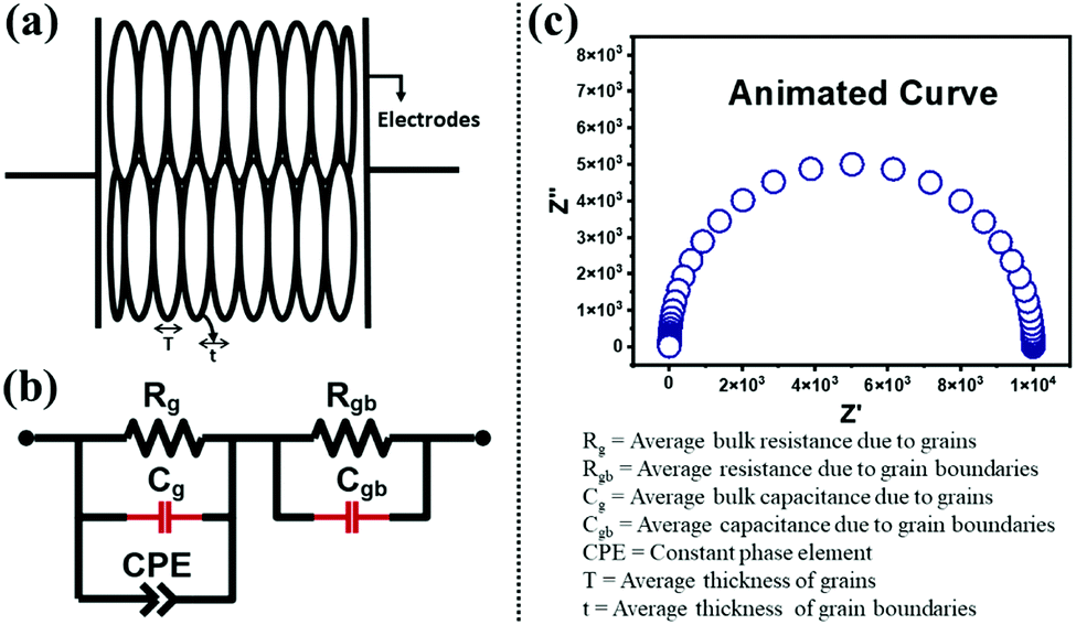 | ||
| Fig. 4 (a) The brick layer model consists of plate-shaped grains to simulate the capacitive and resistive contribution by grains and grain boundaries. (b) The different components contributing to impedance and their equivalent circuit. (c) A simulated Nyquist plot is drawn as according to the equivalent circuit in the frequency range of 1 Hz to 1 MHz. | ||
To obtain an equivalent circuit corresponding to the observed Nyquist plot in the entire frequency range is challenging due to different possible contributions to impedance in the polycrystalline phase. The current approach to evaluate this contribution using a brick-layer model is in good agreement with experimental impedance and also yields realistic values of grain and grain boundary impedance. A semi-circular arc-like Nyquist plot observed in the complex impedance plane was fitted with the simulated Nyquist plot (Fig. 4(c)). The observed impedance for all samples and their corresponding fitted curve (red solid line) are shown in Fig. 5. The lowering of impedance with an increase in temperature can be seen as a reduction in the radius of the semi-circular arc at high temperatures (Fig. 5). Some arcs at high temperature cannot be clearly seen due to the chosen axis-range. This decrease in impedance with temperature is expected due to an increase in the thermally assisted conduction mechanism in ceramic oxides.
 | ||
| Fig. 5 The Nyquist plot (Z′′ vs. Z′) for (a) BBT-AS, (b) BBT-TE, (c) SBT-AS and (d) SBT-TE. The equivalent circuit shown in the inset of (b) and the corresponding curve is used for fitting (red line) in the present study. The direction of the increase in frequency is presented in (c) with a blue dashed curved line. | ||
Comparative data of the extracted values, obtained from the fitting of an equivalent circuit are presented in Table 3. The values of resistance (Rg and Rgb) and capacitance (Cg and Cgb) were taken at a mega-ohm (MΩ) and nano farad (nF) scale respectively. The constant phase element takes into account the departure from ideal Debye-like behaviour. The temperature dependent value of n varies between 0.275–0.406 (0.288–0.39) for BBT (BBT-TE) and 0.406–0.701 (0.497–0.564) for SBT (SBT-TE). The observed values of n indicate the CPE is neither purely resistive nor capacitative but a combination of both. The capacitance range for all samples obtained both below and above the transition temperature is in good agreement with the values of other ferroelectric systems.46 The capacitance and resistance values indicate the samples are well sintered. Furthermore, the overall resistance was observed to be dominated by grains Rg at all temperatures.
| Material name | Temp. (°C) | R g (MΩ) | R gb (MΩ) | C g (nF) | C gb (nF) | n |
|---|---|---|---|---|---|---|
| BBT | 300 | 1 (0.796) | 0.157 (0.211) | 0.385 (0.136) | 0.239 (0.275) | 0.406 (0.39) |
| 350 | 0.191 (0.201) | 0.0735 (0.0427) | 0.318 (0.655) | 2.039 (0.704) | 0.372 (0.315) | |
| 400 | 0.0571 (0.0478) | 0.0206 (0.0182) | 0.040 (0.044) | 2.607 (2.913) | 0.322 (0.331) | |
| 450 | 0.0208 (0.0178) | 0.0071 (0.0065) | 0.865 (0.972) | 0.389 (0.419) | 0.275 (0.283) | |
| 500 | 0.0089 (0.0066) | 0.0029 (0.0038) | 0.170 (0.856) | 2.43 (0.023) | 0.406 (0335) | |
| SBT | 400 | 0.541 (6.987) | 0.154 (0.474) | 0.041 (0.015) | 1.557 (0.037) | 0.432 (0.552) |
| 450 | 0.167 (1.728) | 0.014 (0.274) | 0.093 (0.011) | 0.161 (0.312) | 0.613 (0.497) | |
| 520 | 0.028 (0.338) | 0.0075 (0.023) | 0.752 (0.042) | 0.432 (0.151) | 0.406 (0.549) | |
| 550 | 0.013 (0.17) | 0.0057 (0.0285) | 0.836 (0.044) | 0.214 (0.043) | 0.509 (0.564) | |
| 600 | 0.0052 (0.071) | 0.0023 (0.016) | 0.147 (0.028) | 0.141 (0.03) | 0.701 (0.507) |
The DC component of grain and grain boundary conductivities  plotted with the inverse of temperature (T−1) is shown in Fig. 6.48 These conductivities (σg and σgb) follow the Arrhenius law,
  for grains and
  for grain boundaries, where σ0 is the pre-exponent factor, σg and σgb are the DC conductivities by grain and grain boundary respectively, Eg and Egb are the activation energies of the grain and grain boundary respectively and kB is the Boltzmann constant. The above equations are made linear by taking the natural log of both sides for easy interpretation. The slope of linear fit is then used to obtain the activation energy.
 | ||
| Fig. 6 The DC conductivities due to grain and grain boundary for (a) BBT-AS, (b) BBT-TE, (c) SBT-AS and (d) SBT-TE. The red line represents Arrhenius fitting. | ||
The calculated values of activation energies of σg and σgb are Eg = 0.90 eV, Egb = 0.84 eV for BBT-AS and Eg = 0.91 eV and Egb = 0.78 eV for BBT-TE. However, the Eg and Egb for SBT-AS (SBT-TE) are 0.97 eV (1.17 eV) and 0.99 eV (0.90 eV) respectively. This decrease in activation energy (≈0.01 eV) of σgb in both complex oxides can be correlated with the improved homogeneity in the microstructure of thermally etched pellets. The bulk activation energy of σg for BBT remains nearly the same before and after heat treatment and shows an overall increase in the SBT. This is in good agreement with the decrease in dielectric constant post heat treatment in the SBT-TE samples. The temperature dependent values of dc conductivity, resistance and capacitance indicate that the overall dielectric properties are dominated by the bulk (grain) component in both BBT and SBT.
7 P–E hysteresis loop analysis
The room temperature ferroelectric behaviour of both the materials is illustrated in Fig. 7 with a hysteresis curve of polarization (P) in the presence of an electric field (E). The polling of the sample before studying ferroelectric behaviour in polycrystalline ceramics is a usual practice. However, this aligning of domains during the polling process dominates the overall polarization mechanism. Thus, to observe the contribution due to grains, grain boundaries and other polarization processes, the samples were not polled before the measurement in the present study. A clear hysteresis curve indicates a typical ferroelectric behaviour of Aurivillius oxides at room temperature. | ||
| Fig. 7 The polarization P variation with electric field E, showing a ferroelectric hysteresis behaviour at room temperature for (a) BBT-AS, (b) BBT-TE, (c) SBT-AS and (d) SBT-TE. The inset of all the figures represents the upper half curve and the red line represents Miller fitting of the hysteresis curve. | ||
The experimental polarization loops as a function of electric field were fitted with the following relation suggested by S. L. Miller49,50 with an additional E-field independent loss term.51
| P(E) = Pmiller + Ploss | (7) |
 | (8) |
 | (9) |
 | (10) |
The different values obtained by fitting polarization variation with the E-field are summarized in Table 4. To understand the contribution to polarization by various mechanisms, an approach suggested by H. Yan et al. is utilized.52 In analogy to this model, the polarization in polycrystalline BBT and SBT shows a combined effect of contribution due to the dielectric constant, electric conductivity, and domain switching. The effect of non-ferroelectric components is clearly visible and evaluated by Ploss. The observed reduction in grain size post thermal etching is also evident in the P–E loop with a smaller value of Pr. The heat treatment also slightly improves the texture, which can be seen by the lowering of the coercive field, EC. All the P–E curves are non-saturating and rounded; the non-saturating part is due to electrical permittivity, whereas the rounded curve is an indication of the conductivity contribution in agreement with Fig. 6. Furthermore, the loss factor in both thermally etched samples increases compared to the sintered counterparts. This is attributed to an increase in the grain boundary to grain ratio in the TE samples. The possibility of charge accumulation at the grain boundaries increases and hence contributes toward the losses.
| Sample-name | P S |
|
E C | P loss |
|---|---|---|---|---|
| BBT-AS | 5.03 | 0.987 | 25.48 | 0.145 |
| BBT-TE | 3.12 | 0.99 | 25.03 | 0.259 |
| SBT-AS | 0.14543 | 0.998 | 26.13 | 6 × 10⁻⁵ |
| SBT-TE | 0.122 | 0.97 | 22.85 | 0.131 |
8 Summary
In summary, single phase BaBi4Ti4O15 and SrBi4Ti4O15 have been synthesized and the effect of thermal etching on the structural, dielectric and piezoelectric properties was investigated. The room temperature X-ray diffraction and consequent Rietveld refinement confirms that all the synthesized Aurivillius compounds crystallize to the non-centrosymmetric orthorhombic (pseudo-tetragonal) phase with A21am symmetry. The microstructure shows a significant improvement post thermal etching, with a uniform grain size distribution and reduction in average grain size. However, the effect of this improvement in the microstructure is in contrast with the dielectric properties as the dielectric constant, ε′, was observed to increase for BaBi4Ti4O15 and significantly reduce for SrBi4Ti4O15. Furthermore, an appreciable difference in dielectric relaxation for complete substitution of the non-ferroelectric A-site in BaBi4Ti4O15 with Sr is surprising. The observed transition from the relaxor to ferroelectric phase and large change in transition temperature (from 400 °C to 521 °C) is attributed to the slightly different co-valency and electronic structure of two alkaline earth cations. The contribution due to grain (bulk) and grain boundary is evaluated using a brick-layer model. This model uses an equivalent circuit made of three sub-circuits representing the grain, grain boundary and constant phase element. The grain and grain boundary activation energy indicate that the electrical properties are dominated by grain (bulk) contribution and thus can be controlled by controlling its microstructure. The polarization variation with E-field is explained by a modified Miller expression. It is observed that a mechanism such as dielectric polarization and conductivity also contributes in addition to spontaneous polarization. The observed changes in ferroelectric parameters in thermally etched samples can be corroborated with the microstructure. Thus, the present study suggests that the macroscopic physical and transport properties are highly correlated and the desired properties can be tuned even by a simple single step processing parameter such as thermal etching in m = 4 Aurivillius oxides ([Bi2O2]2+ [Am−1BmO3m+1]2− (A = Ba, Sr)).Author contributions
SSR conceived the work and VKS carried out all the experimental work including synthesis of the samples and writing the original draft. RN and SSR analysed the data and wrote the final manuscript. All authors approved the final manuscript.Conflicts of interest
There are no conflicts to declare.Acknowledgements
The authors acknowledge the Science and Engineering Research Board (SERB), Govt. of India for financial support under sanctioned project no. ECR/2017/002691. The authors also acknowledge the Sophisticated Analytical Instrument Facility (SAIF), Manipal University Jaipur (MUJ) for the FESEM analysis, the User Facility at UGC DAE CSR, Indore for the X-ray diffraction measurements and the Indian Institute of Technology Bombay (IIT Bombay) for the Broadband Dielectric Spectroscopy (BDS) and PE loop measurements.Notes and references
- N. Sezer and M. Koç, Nano Energy, 2021, 80, 105567 CrossRef CAS.
- F. Narita and M. Fox, Adv. Eng. Mater., 2018, 20, 1700743 CrossRef.
- A. Zaszczyńska, A. Gradys and P. Sajkiewicz, Polymers, 2020, 12, 2754 CrossRef PubMed.
- B. C. Sekhar, B. Dhanalakshmi, B. S. Rao, S. Ramesh, K. V. Prasad, P. S. Rao and B. P. Rao, Multifunctional Ferroelectric Materials, Intech open, 2021, vol. 71 DOI:10.5772/intechopen.92527.
- D. Damjanovic, Piezoelectric and acoustic materials for transducer applications, Springer, 2008, pp. 59–79 Search PubMed.
- M. T. Chorsi, E. J. Curry, H. T. Chorsi, R. Das, J. Baroody, P. K. Purohit, H. Ilies and T. D. Nguyen, Adv. Mater., 2019, 31, 1802084 CrossRef PubMed.
- J. Chen, Q. Qiu, Y. Han and D. Lau, Renewable Sustainable Energy Rev., 2019, 101, 14–25 CrossRef CAS.
- B. Narayan, J. S. Malhotra, R. Pandey, K. Yaddanapudi, P. Nukala, B. Dkhil, A. Senyshyn and R. Ranjan, Nat. Mater., 2018, 17, 427–431 CrossRef CAS PubMed.
- W. Qian, W. Yang, Y. Zhang, C. R. Bowen and Y. Yang, Nano-Micro Lett., 2020, 12, 1–39 CrossRef PubMed.
- A. Aabid, B. Parveez, M. A. Raheman, Y. E. Ibrahim, A. Anjum, M. Hrairi, N. Parveen and J. Mohammed Zayan, Actuators, 2021, 10(101), 1–26 Search PubMed.
- A. J. Bell, T. P. Comyn and T. J. Stevenson, APL Mater., 2021, 9, 010901 CrossRef CAS.
- W. H. Organization et al. , 2017.
- A. Han, E. Han and E. Han Hv, 2011.
- A. J. Bell and O. Deubzer, MRS Bull., 2018, 43, 581–587 CrossRef CAS.
- J. Koruza, A. J. Bell, T. Frömling, K. G. Webber, K. Wang and J. Rödel, J. Materiomics, 2018, 4, 13–26 CrossRef.
- H. Wei, H. Wang, Y. Xia, D. Cui, Y. Shi, M. Dong, C. Liu, T. Ding, J. Zhang and Y. Ma, et al. , J. Mater. Chem. C, 2018, 6, 12446–12467 RSC.
- F. Hussain, A. Khesro, Z. Lu, G. Wang and D. Wang, Front. Mater., 2020, 7, 87 CrossRef.
- D. Maurya, M. Peddigari, M.-G. Kang, L. D. Geng, N. Sharpes, V. Annapureddy, H. Palneedi, R. Sriramdas, Y. Yan and H.-C. Song, et al. , J. Mater. Res., 2018, 33, 2235–2263 CrossRef CAS.
- N.-B. Do, H.-B. Lee, C.-H. Yoon, J.-K. Kang, J.-S. Lee and I.-W. Kim, Trans. Electrical Electron. Mater., 2011, 12, 64–67 CrossRef.
- J. Wu, J. Appl. Phys., 2020, 127, 190901 CrossRef CAS.
- F. Hussain, A. Khesro, Z. Lu, G. Wang and D. Wang, Front. Mater., 2020, 7, 87 CrossRef.
- T. Takenaka, K. Komura and K. Sakata, Jpn. J. Appl. Phys., 1996, 35, 5080 CrossRef CAS.
- H. Sun, Y. Wu, X. Xie, Y. Lu, T. Yao, J. Zhong and X. Chen, J. Materiomics, 2018, 4, 353–359 CrossRef.
- G. Nalini and T. G. Row, Bull. Mater. Sci., 2002, 25, 275–281 CrossRef CAS.
- B. J. Kennedy, Q. Zhou, Y. Kubota and K. Kato, et al. , J. Solid State Chem., 2008, 181, 1377–1386 CrossRef CAS.
- E. Subbarao, J. Am. Ceram. Soc., 1962, 45, 166–169 CrossRef CAS.
- C. H. Hervoches, A. Snedden, R. Riggs, S. H. Kilcoyne, P. Manuel and P. Lightfoot, J. Solid State Chem., 2002, 164, 280–291 CrossRef CAS.
- C. García de Andrés, F. Caballero, C. Capdevila and D. San Martín, Mater. Charact., 2002, 49, 121–127 CrossRef.
- U. Täffner, V. Carle, U. Schäfer and M. J. Hoffmann, Metallography and Microstructures, ASM International, 2004 Search PubMed.
- J. Hu, X. Wang, J. Zhang, J. Luo, Z. Zhang and Z. Shen, J. Materiomics, 2021, 7, 1007–1013 CrossRef.
- T. Kimura, J. Ceram. Soc. Jpn., 2016, 124, 268–282 CrossRef CAS.
- L. K. Pradhan and M. Kar, author, 2021.
- Y. Chen, K. H. Liu, Q. Luo, M. Mei, G. L. Chen, R. K. Pan, Y. J. Qi and W. Q. Cao, J. Appl. Phys., 2019, 125, 184104 CrossRef.
- A. K. Jonscher, J. Phys. D: Appl. Phys., 1999, 32, R57–R70 CrossRef CAS.
- L. E. Cross, Ferroelectrics, 1987, 76, 241–267 CrossRef CAS.
- T.-F. Zhang, X.-X. Huang, X.-G. Tang, Y.-P. Jiang, Q.-X. Liu, B. Lu and S.-G. Lu, Sci. Rep., 2018, 8, 1–12 CrossRef.
- V. K. Sharma, R. Nathawat and S. S. Rathore, 2021 IEEE International Symposium on Applications of Ferroelectrics (ISAF), 2021, pp. 1–4 Search PubMed.
- M. Trainer, Eur. J. Phys., 2000, 21, 459–464 CrossRef CAS.
- D. Y. Suárez, I. M. Reaney and W. E. Lee, MRS Online Proc. Libr., 2000, 658, 1191–1196 Search PubMed.
- N. A. Benedek, J. M. Rondinelli, H. Djani, P. Ghosez and P. Lightfoot, Dalton Trans., 2015, 44, 10543–10558 RSC.
- R. Machado, M. Stachiotti, R. Migoni and A. H. Tera, Phys. Rev. B: Condens. Matter Mater. Phys., 2004, 70, 214112 CrossRef.
- A. Roy, R. Prasad, S. Auluck and A. Garg, Appl. Phys. Lett., 2013, 102, 182901 CrossRef.
- S. Bobade, D. Gulwade, A. Kulkarni and P. Gopalan, J. Appl. Phys., 2005, 97, 074105 CrossRef.
- A. Elbasset, S. Sayouri, F. Abdi, T. Lamcharfi and L. Mrharrab, Glass Phys. Chem., 2017, 43, 91–97 CrossRef CAS.
- S. Huang, C. Feng, L. Chen and Q. Wang, J. Am. Ceram. Soc., 2006, 89, 328–331 CrossRef CAS.
- J. T.-S. Irvine, D. C. Sinclair and A. R. West, Adv. Mater., 1990, 2, 132–138 CrossRef CAS.
- J.-B. Jorcin, M. E. Orazem, N. Pébère and B. Tribollet, Electrochim. Acta, 2006, 51, 1473–1479 CrossRef CAS.
- R. Tang, C. Jiang, W. Qian, J. Jian, X. Zhang, H. Wang and H. Yang, Sci. Rep., 2015, 5, 13645 CrossRef CAS PubMed.
- S. L. Miller, R. D. Nasby, J. R. Schwank, M. S. Rodgers and P. V. Dressendorfer, J. Appl. Phys., 1990, 68, 6463–6471 CrossRef.
- C. H. Tsang, C. K. Wong and F. G. Shin, J. Appl. Phys., 2005, 98, 084103 CrossRef.
- K. Bhoi, H. Mohanty, M. F. Abdullah, D. K. Pradhan, S. N. Babu, A. Singh, P. Vishwakarma, A. Kumar, R. Thomas and D. K. Pradhan, et al. , Sci. Rep., 2021, 11, 1–17 CrossRef PubMed.
- H. Yan, F. Inam, G. Viola, H. Ning, H. Zhang, Q. Jiang, T. Zeng, Z. Gao and M. J. Reece, J. Adv. Dielectr., 2011, 01, 107–118 CrossRef CAS.
| This journal is © The Royal Society of Chemistry 2022 |