
 Open Access Article
 This Open Access Article is licensed under a Creative Commons Attribution-Non Commercial 3.0 Unported Licence
Spin reorientation transition driven by polaronic states in Nd2CuO4
Soma
Banik
 *ab,
Kritika
Vijay
ab,
Suvankar
Paul
a,
Najnin
Mansuri
c,
D. K.
Shukla
c,
S. K.
Srivastava
a,
Archna
Sagdeo
ab,
Kranti
Kumar
c,
Shilpa
Tripathi
d and
S. N.
Jha
bd
*ab,
Kritika
Vijay
ab,
Suvankar
Paul
a,
Najnin
Mansuri
c,
D. K.
Shukla
c,
S. K.
Srivastava
a,
Archna
Sagdeo
ab,
Kranti
Kumar
c,
Shilpa
Tripathi
d and
S. N.
Jha
bd
aSynchrotrons Utilization Section, Raja Ramanna Centre for Advanced Technology, Indore, 452013, India. E-mail: soma@rrcat.gov.in; somasharath@gmail.com
bHomi Bhabha National Institute, Training School Complex, Anushakti Nagar, Mumbai, 400094, India
cUGC-DAE Consortium for Scientific Research, Khandwa Road, Indore 452001, India
dBeamline Development and Application Section, Bhabha Atomic Research Center, Mumbai, 400085, India
First published on 25th July 2022
Abstract
We show that the spin reorientation transition in Nd2CuO4 is due to the electronic interactions between the bulk and the surface. Electron-like doping due to the small oxygen deficiency in Nd2CuO4 gives rise to the localized Nd2+ states on the surface while the bulk has dominating Nd3+ states. Nd2+ states act like bound polaronic in-gap states on the surface, which are hybridized with the Cu–O charge transfer band. Polaron–polaron interactions lead to ferromagnetic correlations and also decrease the energy gap across the spin reorientation transition. Drastic variation in the density of states along with valence band narrowing at low temperature indicates the bulk–surface interaction between the Nd3+ and Nd2+ states through the Cu–O spin cloud. Short range electron–lattice interaction due to the bound polaronic states with large negative Seebeck coefficient (−535 μV K−1 at 300 K) suggests electron doped Nd2CuO4 as a potential thermoelectric material.
1 Introduction
Polarons are among the most fundamental quasiparticles in the interacting many body systems, which are formed due to the local distortion of the lattice induced by charge carriers.1 The polaron hopping mechanism of charge transfer has many important applications in thermoelectrics, photovoltaics, two-dimensional electron gas transistors, spin valve devices, magnetic sensors and magnetic memories etc.1–5 In high temperature superconducting materials, the magnetic polarons are predicted to form around the charged dopants in an antiferromagnetic background with low doping concentration.6 Nd2CuO4 (NCO) is a charge-transfer insulator7 with antiferromagnetic ground state.8 The copper moments in NCO order antiferromagnetically around TN = 245–255 K.9,10 The 3D oriented spins in the CuO layer undergo a series of complicated reorientation transitions due to induced ordering of the rare-earth magnetic moments at 75 K and 30 K.8–11 Doping holes or electrons by chemical substitution in a single layer copper-oxide transforms the parent antiferromagnetic insulator to an exotic metal with superconductivity.12 However, no metallicity is reported in the bulk undoped NCO.13 High-temperature conductivity showed n-type charge carriers in the parent NCO.14The average oxidation state of Cu in NCO is one of the dominant factors governing the electronic conductivity. Cluster calculations showed a metallic ground state for the electron-doped NCO which can be obtained by oxygen deficiency.15 In a recent experimental report, metallicity in the undoped NCO thin films has been obtained by post growth annealing.16 In the T′ structure of NCO the excess oxygen ions occupy the interstitial site in the Nd2O2 layer while the oxygen deficiency occurs in the CuO2 layer.12 Dominant electronic charge carriers in NCO can either be electrons or holes14 depending on the oxygen stoichiometry and have distinct signatures in the electronic structure.15,16 Electron doping due to the oxygen deficiency in NCO has a strong tendency to form polaronic states.17–19 However, experimental observation of the internal structure of polarons and its electronic properties in NCO are lacking.
NCO behaves like a Slater insulator with magnetic-order driven electronic states and weak electron–electron correlation.20 In general insulator to metal transitions in cuprates have been theoretically associated with the change in the bond lengths and the angles.21 However, experimental observation indicates the interplay between the electron–electron correlation (Mott type) and electron–phonon interactions.21 Very recently, thermal Hall conductivity on NCO showed the existence of phonon chirality that leads to a large conductivity at low temperature.22 It is attributed that the phonon chirality arises from an intrinsic coupling of phonons to their environment22 but whether the phonon is coupled to the charge or the spin of the electron is not clearly known.
The 2-dimensional layered tetragonal T′ structure in NCO23 predicts the distinct nature of the electron–phonon and the electron–electron interactions on the surface and the bulk.24 This motivated us to determine the electronic structure of the surface and the bulk separately in NCO. Application of synchrotron radiation gives the possibility to tune the photoelectron escape depth via the kinetic energy allowing for surface and bulk-sensitive detection of the electronic structure. So, in this work we have measured the valence band and core levels of NCO using photoemission at the bulk and surface sensitive excitation energies. The partial density of Nd 4f and Cu 3d states at the surface and bulk have been determined from resonant photoemission (RPES) measurements. From our experimental results, we have clearly explained the role of electron–electron interactions at the surface and the bulk responsible for the spin reorientation transitions and the role of polaronic states in NCO.
2 Methodology
The bulk ingot of Nd2CuO4 was prepared using the solid state reaction method. The Nd2O3 powder (99.99% purity) was pre-annealed at 1000 °C for 10 hours. The pre-annealed Nd2O3 powder is then mixed with the CuO powder using mortar and pestle for 3 hours followed by annealing in air at 1000 °C for 24 hours. Small pieces are cut from the bulk ingot and ground into fine powder for X-ray diffraction (XRD) measurements. Lab based XRD was performed using a commercial X-Ray diffractometer from a Bruker model D8 Advance with a Cu Kα source. Detailed temperature dependent synchrotron XRD measurements using 15 keV excitation energy were performed at the angle-dispersive X-ray diffraction (ADXRD) beamline at the Indus-2 synchrotron radiation source. Low temperature has been achieved using a liquid helium-based flow-type cryostat with the temperature stability of 0.15 K. A high spectral resolution of about 1 eV at 10 keV was achieved using a Si(111) based double crystal monochromator. Powder XRD patterns were recorded using an Image plate Mar-345 detector. The photon energy and the sample to detector distance were accurately calibrated using the LaB6 NIST standard. Fit2D software was used to generate the XRD pattern from the diffraction rings obtained by Image plate data. Le Bail decomposition of the XRD pattern was carried out using the JANA2000 package.25 Resistivity measurement was done in the standard four point configuration by using a Keithley 2401 current source, Keithley 2182 nanovoltmeter and cryocon temperature controller. Thermopower measurement was done through controlled heat pulses, as detailed in ref. 26, by using a cryocon temperature controller and Keithley 2182 nanovoltmeter. The magnetic measurement was performed using a commercial SQUID magnetometer (MPMS XL, M/s. Quantum Design, USA) in a zero field cooled protocol. The RPES across Cu 3p–3d resonance was performed at the Angle Resolved Photoelectron Spectroscopy beamline (ARPES BL-3), Indus-1 using a Phoibos 150 electron energy analyzer. The sample was cleaned by mechanical scrapping with a diamond file for all the photoemission measurements. The base vacuum in the ARPES BL-3 analysis chamber was ∼3 × 10⁻¹⁰ mbar. The valence band (VB) spectra were recorded by varying the photon excitation energies from 66 eV to 95 eV across the Cu 3p–3d transition with the energy resolution of 135 meV. High resolution RPES measurements across the Nd 4d–4f resonance in the energy range from 118 eV to 142 eV with the energy resolution ∼40 meV were performed at the undulator based Angle Resolved Photoelectron Spectroscopy beamline (ARPES BL-10), Indus-2. RPES across the Nd 3d–4f and Cu 2p–3d with an energy resolution of 300 meV were also measured at ARPES BL-10, Indus-2. The VB spectra across the Nd 3d–4f transition were recorded by varying the photon excitation energies from 967 eV to 988 eV and those across the Cu 2p–3d resonance were recorded by varying the photon excitation energies from 930 eV to 938 eV. Synchrotron core level spectra (SR-XPS) were recorded at hν = 1078 eV with 0.5 eV energy resolution and compared with the core level spectra measured with the Lab XPS Al Kα source (hν = 1486.6 eV) from SPECS (XR 50) with 0.9 eV energy resolution. Temperature dependent valence band measurements with high energy resolution were performed using the monochromatic He-1 line from a SPECS UVS 300 source.27 The binding energy scale was calibrated with the Ag 3d lines and Fermi edge following the standard procedure.28,29 Both the VB and the XPS data were recorded with a SPECS Phoibos 150 electron energy analyzer. The base vacuum in the analysis chamber of ARPES, BL-10 was 7 × 10⁻¹¹ mbar.3 Results and discussion
The powder XRD pattern of NCO recorded with a Cu Kα source in Fig. 1 shows a single phase tetragonal T′ structure with I4/mmm space group. The lattice parameters determined by the Le Bail refinement: a = 3.942(5) Å and c = 12.163(4) Å are in good agreement with the lattice parameters reported in the literature.13,30 The structural parameters in NCO are highly depend on the oxygen stoichiometry. Similar lattice parameters reported in ref. 30 have been found to be slightly oxygen deficient with the signature of small polarons in thermopower measurements. | ||
Fig. 1 XRD pattern of Nd2CuO4 recorded using a Cu Kα source in (a) showing dots for the experimental data, solid black line for the calculated pattern using the Le Bail refinement method and dashed lines for the difference between the experimental and the calculated pattern. The crystal structure is shown in the inset of (a). Temperature dependence of resistivity is shown in (b) with the inset showing the log![[thin space (1/6-em)]](https://www.rsc.org/images/entities/char_2009.gif) ρ vs. 1/kT plot to estimate the energy gap (EG) at high and low temperature regimes. The Seebeck coefficient as a function of temperature is shown in (c). The arrows in (b) and (c) indicate the antiferromagnetic transition temperature (TN). ρ vs. 1/kT plot to estimate the energy gap (EG) at high and low temperature regimes. The Seebeck coefficient as a function of temperature is shown in (c). The arrows in (b) and (c) indicate the antiferromagnetic transition temperature (TN). | ||
The resistivity (ρ) versus temperature (T) in Fig. 1(b) shows typical semiconducting behavior with 1.5 Ω cm at 400 K and 88 Ω cm at 100 K. In semiconductors, the temperature dependent resistivity follows the exponential form: ρ(T) = ρ0exp(EG/kT) where ρ0 is the residual resistivity, EG is the band gap energy, k is Boltzmann's constant and T is the temperature. So, to determine the band gap energy EG we have plotted logρ versus 1/kT as shown in the inset of Fig. 1(b) and the linear fitting (solid lines) shows different slopes at high T and low T regime. The slopes indicate the values of EG, which are found to be lower (EG1 ≈ 11.3 ± 0.02 meV) at the low temperature region than that in the high temperature region (EG2 ≈ 40.8 ± 0.03 meV). Decrease in EG with temperature is an anomalous behavior also reported in silicon31 and has been attributed to the electron–phonon renormalization. Increase in conductivity due to electron–phonon interaction is well reported in NCO.22 Enhancement in charge carriers can also occur due to the presence of small polarons in NCO.18,30 Small polarons are relatively localized but the adiabatic hopping of the polarons not only causes polarization in the neighboring lattice but also increases the charge carriers.18 The non linear resistivity in Fig. 1(b), shows an inflection point at ≈180 K (marked by tick in Fig. 1(b)) which may be related to the magnetic transition. Anomalous behavior in resistivity indicates different character of charge carriers at low and high temperature regimes.
Thermopower is an effective tool to determine the nature of charge carriers. Generally in a semiconductor at high temperature, electrons will have enough energy to excite across the band gap and hence the resultant thermopower (S) will have a compensated effect due to both n-type carriers in the conduction band and p-type carriers in the valence band. This phenomenon leads to reduced S in NCO above 200 K (Fig. 1(c)). We find that S is almost constant in the temperature range from 180 K to 210 K and below 180 K there is a sharp decrease, which may be associated with the magnetic transition. We find that the value of S is negative in the whole temperature range from 100–320 K indicating the electron-like carriers in NCO and hence it is an n-type semiconductor. The more negative value of S ≈ −603 μV K−1 at 100 K than S ≈ −535 μV K−1 at 300 K indicates the increase in the localization effect with the magnetic transition, which needs to be explored.
3D magnetic structure of NCO was revealed from neutron-scattering experiments.8 However, the analysis of the 3D transition through pure magnetic measurements is usually difficult, because the Cu antiferromagnetic sublattice carries a very small signal. In Fig. 2(a) we have shown the M versus T curve for NCO measured in 0.5 T magnetic field. Our M–T data shows a very good agreement with the M–T curve generated from the neutron scattering measurements as reported in ref. 33. The molar magnetic susceptibility (χm) has been estimated from the value of magnetization (M) and the external field (H) using the formula: χm = M/H. To extract the weak magnetic signals we have shown the plot of second derivative ( ) versus T in Fig. 2(b) in the temperature range between 100–300 K. We find that the antiferromagnetic transition TN ≈ 225 K for NCO is slightly less than the reported TN (≈255 K) from neutron scattering in ref. 8, which indicates the oxygen non-stoichiometry in this system. Both the electron or hole doping in NCO has been reported to decrease the TN.34
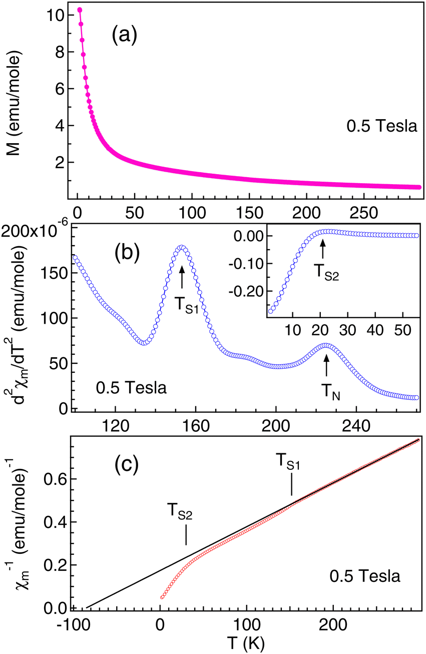 | ||
Fig. 2 The dependence of temperature on magnetization at 0.5 Tesla field is shown in (a). The second derivative of molar susceptibility  in the temperature range between 100 K to 300 K is shown in (b). Inset of (b) shows the in the temperature range between 100 K to 300 K is shown in (b). Inset of (b) shows the  versus T in the energy range from 2 K to 60 K. TN denotes the antiferromagnetic ordering temperature while TS1 and TS2 are the spin reorientation transition temperatures. Inverse molar susceptibility (χm−1) as a function of temperature is shown in (c). The solid line in (c) is the fitting using the Curie–Weiss law. versus T in the energy range from 2 K to 60 K. TN denotes the antiferromagnetic ordering temperature while TS1 and TS2 are the spin reorientation transition temperatures. Inverse molar susceptibility (χm−1) as a function of temperature is shown in (c). The solid line in (c) is the fitting using the Curie–Weiss law. | ||
Hole doping in NCO can only be achieved by having excess oxygen stoichiometry.15 The doped holes are believed to enter into the oxygen p-orbitals in the CuO2 planes. In electron doped cuprates however, the extra electrons induced by doping are believed to enter into the d-orbital of Cu, giving rise to spin-less Cu+-ions that dilute the background antiferromagnetic Cu2+–Cu2+ coupling without inducing as strong spin frustrations as those in the hole-doped cuprates. Electron doping can be achieved by reduction annealing in which one can either create vacancies at the regular oxygen sites or fill the Cu vacancies.16 Here, preannealing during the sample preparation may have caused very small oxygen deficiency in this system and indicates the possibility of the polaronic states.
In addition, we have also observed two strong spin-reorientation transitions at 153 K (marked as TS1 in Fig. 2(b)) and at 21 K (marked as TS2 in the inset of Fig. 2(b)). The onset of TS1 at about 180 K matches with the onset of the magnetic transition observed in the thermopower measurements (Fig. 1(c)). Analysis of χm−1 was performed in the high T region from 300 K to 160 K using the Curie–Weiss law of the form:  . Here, C is the Curie–Weiss constant and θ is the characteristic Curie–Weiss temperature. The curve fitting at higher T yields C = 490.485 emu K mol−1, and θ = −85.4 K. Large value of C indicates the coupling between Cu and Nd magnetic moments. The negative value of θ is associated with the long range antiferromagnetic correlations while the downward curving of χm−1 at TS1 and TS2 indicates the short range ferromagnetic correlations associated with the spin-reorientation transitions. It is reported that the polaron–polaron interaction is ferromagnetic while the carrier–carrier interactions are antiferromagnetic in the magnetic semiconductors.35 Moreover, there can be abrupt transition between the bound magnetic polarons depending on the strength of the exchange coupling between the electron spin of the carrier and local moments.36 In parent NCO the spin reorientation transitions have been explained in terms of the competition between various Nd–Nd and Nd–Cu–Nd interplanar interactions.33
To explore the possibility of the interplanar interaction associated with the spin-reorientation transitions, we have performed temperature dependent XRD measurements, as shown in Fig. 3(a). The data has been collected in the heating cycle. We have considered the (004) peak as the reference peak (marked by *) and normalized all the XRD patterns at different temperatures at this intensity. No structural changes were observed as a function of temperature and similar results have been reported in ref. 8 and 12. The lattice parameters determined using Le Bail refinement show an ≈0.2 ± 0.05% decrease in both a and c (Fig. 3(c and d)) in the temperature range from 300 K to 5 K. We have observed a clear intensity variation in the (103), (110) and (213) peaks in Fig. 3(b) with the onset of TS1 ≈ 180 K (marked by arrow). The maximum intensity in the XRD peaks is observed at around spin-reorientation transitions TS1 and TS2 (marked by horizontal ticks). Similar such intensity variation has been reported for the magnetic peaks from neutron scattering measurements in NCO and attributed to the spin orientation of the Nd and Cu ions.8 Increase in the intensity of the XRD peaks at low temperature has also been observed by us for other rare-earth systems like CeAg2Ge237 and PrGe38 associated with the itinerant electron magnetism. Hence, the observed changes in the XRD peaks, S and χm across the spin reorientation transitions are associated with the electronic interactions.
 | ||
| Fig. 3 Synchrotron radiation XRD at 15 keV on the powder Nd2CuO4 sample recorded as a function of temperature and shown in (a) for the heating cycle. Reference peak for normalization is marked by * in (a). The contour plot of the diffraction peaks with temperature is shown in (b). The arrow in (b) indicates the TN while the horizontal ticks represent the spin orientation temperatures. The variation of the lattice parameters a and c as a function of temperature in the heating cycles are shown in (c) and (d), respectively. | ||
To understand the role of Nd, Cu and O electrons in the itinerant electron magnetism in NCO, we have performed high resolution valence band (VB) measurements, as shown in Fig. 4(a), at 300 K (RT) in the paramagnetic phase and 20 K (LT) just below TS2 (in Fig. 2(b)) in the antiferromagnetic phase. Both the spectra are normalized at the VB minimum around 8.5 eV binding energy (BE). Five prominent features are observed at around 1 eV, 3.7 eV, 5 eV, 6.2 eV and 7.2 eV which are marked as A, B, C, D and E in Fig. 4(a). Drastic changes have been observed in the VB between RT and LT across the magnetic transitions. Features C and D are the non-bonding and bonding bands of O 2p, which are hybridized with the Cu 3d and Nd 4f states. We find that the intensity of the features A, C and D enhances at LT with a clear density of states near the Fermi level EF (see inset in Fig. 4(a)). The valence bandwidth also decreases at LT indicating the enhancement of the localization effect, which corroborates with the thermopower measurements (Fig. 1(c)).
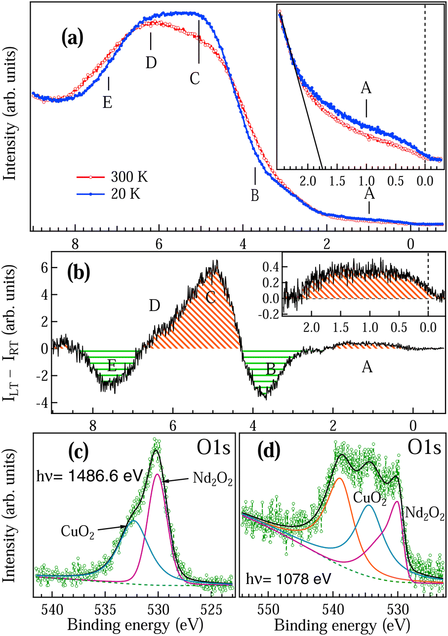 | ||
| Fig. 4 UPS He-1 data showing (a) VB recorded at RT (300 K) and LT (20 K). Inset of (a) shows the zoomed-in region near the EF. (b) shows the difference spectrum obtained by subtracting the VB intensity at RT(IRT) from LT(ILT). Inset in (b) shows the zoomed-in difference spectrum near EF. (c) and (d) show the O 1s core level recorded using 1486.6 eV and 1078 eV excitation energies. | ||
The feature A is related to the charge transfer band and has also been reported by angle resolved photoemission measurements.39 The optical gap reported in this system ranges between 1.2–2 eV12,32 depending on the oxygen concentration. We have determined the valence band maximum from the cutoff for the lowest binding energy (solid line in the inset of Fig. 4(a)). In the n-type semiconductor, the EF lies in the conduction band and hence the optical gap obtained in this system is ≈1.75 eV. We find that the optical gap remains constant across the magnetic transitions. The features B and E show depletion in the density of states at LT which indicates that there is a charge transfer from the bonding B and E states to non-bonding A and C states. The difference spectrum has been plotted in Fig. 4(b) by subtracting the RT spectrum from the LT spectrum as in Fig. 4(a). It is clear from Fig. 4(b) that there are two different characteristic density of states (DOS) as shown by the shaded red region for A, C and D and shaded green region for B and E which are spatially apart.
The increase in DOS near EF at LT is clearly visible in the zoomed-in region of the difference spectra, as shown in the inset of Fig. 4(b). DFT calculations for the electron-doped NCO showed that the Cu 3d states and O 2p states are strongly hybridized and the small DOS around 1 eV (feature A) is the signature of electron doping in this system15,17 while for undoped and hole-doped NCO the feature A near EF is missing.15 Hence, the state A is the polaron state, which is trapped inside the bulk optical gap (≈1.75 eV). We find that the EG determined from resistivity is much smaller (≈11.3 meV at LT) than the bulk optical gap because in the polaronic picture, the energy gap is associated with the energy difference between the localized polaronic band and the conduction band.1 It is also observed that the resistivity showed a semiconducting behaviour (Fig. 1(b)) while a small DOS is obtained in the VB LT spectrum at EF (Fig. 4(a and b)). This observation clearly indicates that the bulk is semiconducting in Nd2CuO4 while the polaronic states are on the surface. Increase in the DOS near EF at LT is associated with the conductivity due to the electron hopping between adjacent localized polaronic states.1
In Fig. 4(c and d) we have measured the O 1s core level at the bulk sensitive (hν = 1486.6 eV) and surface sensitive (hν = 1078 eV) excitation energies to understand the role of oxygen deficiency in NCO. The probing depth at hν = 1486.6 eV is about 25 Å (≈2 monolayers) while with hν = 1078 eV the probing depth is 13 Å (≈1 monolayer). The bulk O 1s peak in Fig. 4(c) clearly shows the contribution due to the Nd2O2 and CuO2. The ratio of the peak area for Nd2O2:CuO2 in the bulk is 0.36:0.64 and on the surface is 0.45:0.55 which shows a good agreement with the reported values of Nd2O2:CuO2 = 0.46:0.54 for NCO thin films in ref. 16. We also find a very broad contribution of an extra oxygen peak at 540 eV binding energy on the surface, which clearly indicates the 2D nature of the oxide. Similar 2D nature of oxygen in the gas phase is reported for the oxygen adsorbed Pd(111) surface.40 Core level of O2 gas near ambient pressure was also reported to show peaks at 539 eV and 540 eV.41 The splitting of the O2 gas-phase peaks occurs due to the paramagnetic nature of the O2 molecule.41 Within our experimental resolution we find that the core polarization of oxygen peaks on the surface is not distinguishable in NCO. However, the presence of the gas-phase peak on the surface indicates the presence of 2D electron gas nature in this material.
To understand the nature of Nd 4f electrons at the surface, we have performed the RPES experiments across Nd 4d–4f resonance. VB spectra of NCO recorded in the energy range from 118 to 142 eV are shown in Fig. 5(a). All the spectra are normalized at the intensity minimum (∼13 eV). Five prominent features were observed in the VB region at 1 eV, 2.8 eV, 4.8 eV, 6 eV and 8.3 eV marked as T, U, V, W and X. To clearly identify the Nd 4d–4f resonances we have also recorded two core levels Y and Z corresponding to Nd 5p at 19 eV and O 2s at 23 eV, respectively. At the off-resonance energy at 118 eV the VB shows dominating Cu 3d states centered at 5 eV. As the incident photon energy is increased we can see considerable changes in the spectral shape in Fig. 5(a); in particular, the features V and X show enhanced intensity around 130 eV and 134 eV while the VB features U and core-levels Y and Z show maximum intensity around 122 eV and 134 eV. All the observations are quite prominent in the contour plot shown in Fig. 5(b) with the resonance features (F1, F2 and F3) marked by dotted lines. Constant initial state (CIS) spectra of the valence band features are shown in Fig. 5(d–h). The CIS intensity plots are obtained from Fig. 5(a) by plotting the normalized intensity at constant BE position. The solid lines in Fig. 5(d–h) are the fitted Fano line shapes.42 The VB structures between 0–4 eV are attributed to the 4f4 → 4f3 transition corresponding to Nd2+ states and 4–9 eV structures are attributed to the 4f3 → 4f2 transition corresponding to the Nd3+ states.44 The trivalent (3+) state with 4fn initial state configuration is a quite stable state in the Nd metal while the divalent (2+) state with 4fn+1 initial state configuration can be resulting from the states near the surface, which is quite probable in rare-earth atoms.44 Moreover, the 4fn+1 configuration in final-state may also arise due to the hybridization between the Nd 4f state and the conduction band state in the initial and the final states.44 CIS spectra in Fig. 5(d–h) clearly showed different resonance energies for Nd2+ at ∼122 eV (marked by F1 in Fig. 5(b and d)) and Nd3+ at ∼130 eV (marked by F2 in Fig. 5(b–f)). The Nd2+ contribution decreases with increasing binding energy in the valence band region (see Fig. 5(d) to 4(f)). The Nd3+ states in Fig. 5(e and f) show multiplet structures with the main components ascribed to the 6H5/2 and 6F5/2 terms around 130 eV and 134 eV, respectively (marked by F2 and F3 in Fig. 5(b–f)). The multiplet feature shows enhanced intensity at 4.8 eV binding energy (see feature V in Fig. 5(a,b,e)) which is in good agreement with the calculated multiplet energy in Nd metal using the Hubbard-I approximation.43 The origin of the multiplet structure is related to many electron phenomena and indicates that the localized Nd3+ 4f electrons interact with the conduction electrons and give rise to delocalized electrons. The multiplet structure is not so prominent near EF (Fig. 5(d)) and in the core levels (Fig. 5(g and h)). However, the signatures of stable Nd2+ and Nd3+ states are observed in the Nd 5p (Fig. 5(g)) and O 2s (Fig. 5(h)) core-levels.
 | ||
| Fig. 5 RPES data recorded across Nd 4d–4f resonance with the valence band features marked in (a). Contour plot as a function of incident photon energy and the binding energy across the Nd 4d–4f resonance for NCO shown in (b). The color scale in (b) represents the intensity as obtained in (a). Nd 4d core levels recorded at 1486.6 eV and 1078 eV photon energies are shown in (c). The constant initial state of the resonant feature U, V, X, Y and Z as a function of incident photon energy shown in (d) to (h), respectively. F1, F2 and F3 are the prominent resonance features. | ||
All the fitted Fano parameters for the F1, F2 and F3 line shapes are listed in Table 1. The large values of q parameter for all the valence band and core level features indicate that both the contributions from Nd2+ and Nd3+ states are localized in nature. The negative and positive value of q is because the minimum in the absorption cross section has occurred on either the high-energy side of the resonance energy or lower side of the resonance energy and depends on the hybridization and the screening effects.27 The negative q parameter of the Nd2+ state and positive q parameter of the Nd3+ state for feature U indicate that the localized Nd2+ 4f states are screened by the 4f conduction electrons, while the Nd3+ states are hybridized with the Cu–O conduction electron. On the other hand, the positive q parameter of the Nd2+ state and both negative and positive q parameter of the Nd3+ state for the feature V (at 4.8 eV in Fig. 5(e)) indicate that the Nd2+ 4f states are strongly hybridized with Nd3+ 4f states with very large value of Γ. The variation in the resonance energy E0 and the Γ mainly depends on the hybridization strength and the orbital overlap.27 Similar resonance energy and multiplet structures are also reported in Nd2O3.45
| E B (eV) | F1 | F2 | F3 | ||||||
|---|---|---|---|---|---|---|---|---|---|
| q | E 0 | Γ | q | E 0 | Γ | q | E 0 | Γ | |
| 2.8 | −5.43 | 121.79 | 1.37 | — | — | — | 5.23 | 132.91 | 2.03 |
| 4.8 | 6 | 121.5 | 7 | 4 | 129.5 | 1.7 | −3.7 | 134.4 | 1.5 |
| 8.3 | — | — | — | 1.4 | 127.4 | 4.5 | −5.4 | 134.7 | 2.9 |
| 19 | −5.4 | 123.3 | 1.7 | — | — | — | 11 | 133.25 | 2.7 |
| 23 | −7.4 | 122.8 | 2 | — | — | — | 11 | 133.25 | 2.7 |
Nd 4d core levels at 1078 eV and 1486.6 eV are shown in Fig. 5(c). We can clearly see that the Nd 4d core-level is much broader in the case of 1078 eV than for 1486.6 eV with the feature corresponding to 4fn+1 and the surface contribution (S) having quite enhanced intensity. Broadening of the core-level peak is related to the life-time broadening and indicates that the DOS at the surface has smaller life time than that of the bulk. Moreover the enhanced intensity of both 4fn+1 and S at the surface indicates that hybridization of the Nd 4f electrons with the conduction band is much stronger at the surface. These observations indicate that the Nd2+ are mainly the polaronic states on the surface while the bulk has a stable Nd3+ configuration. Hence, the magnetic transitions are associated with the polaron–polaron interactions, polaron–carrier interaction and carrier–carrier interaction. Electron doping in NCO has been reported to show the topological phase transitions;46,47 however, topological phases in the electron-doped NCO due to very small oxygen deficiency have not been explored so far.
The RPES data recorded across Cu 3p–3d resonance in the energy range from 66 to 95 eV are shown in Fig. 6(a). Three prominent features are observed in the VB region around 4 eV, 6 eV and 10 eV are marked as A, B and C. Changes in the spectral shape in Fig. 6(a) with a broad Cu 3d resonance region are clearly seen in the contour plot in Fig. 6(b). The CIS intensity at 5 eV BE is shown in the inset of Fig. 6(b) with the open circles showing the experimental data points and the solid line showing the fitted Fano line shape.42 We find that the broad resonance feature is due to Cu 3p1/2 and Cu 3p3/2 threshold with additional resonance at lower photon energy due to the charge transfer type Cu 3dn+1 configuration. The resonance energies E0 obtained for Cu 3p1/2, Cu 3p3/2 and Cu 3dn+1 thresholds are 82.2 eV, 76.8 eV and 72.3 eV, respectively, with the q values 4.95, 4.89 and 4.74 and Γ values 10.4, 13.1 and 13.8, respectively. The large value of q indicates that the Cu 3d states are localized in nature. In Fig. 6(c) we have shown the Cu 3p core level spectra recorded at surface sensitive 1078 eV and bulk sensitive 1486.6 eV excitation energies. Similar to the Nd 4d core level discussed in Fig. 5(c), we find that the 1078 eV spectrum of Cu 3p is much broader than the 1486.6 eV spectrum and the intensity of the charge transfer satellite is quite enhanced at the surface, which indicates that there is a charge transfer from bulk to surface responsible for the carrier mobility and the changes in the Fermi surface topology.
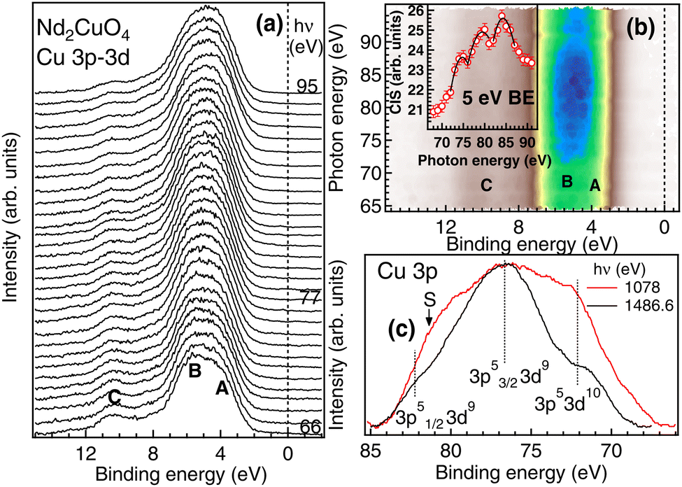 | ||
| Fig. 6 RPES data recorded across Cu 3p–3d resonance with the valence band features marked in (a). Contour plot as a function of incident photon energy and the binding energy across the Cu 3p–3d resonance for NCO is shown in (b). The color scale in (b) represents the intensity as obtained in (a). The constant initial state of the resonant feature at 5 eV BE as a function of incident photon energy is shown in the inset of (b). Cu 3p core levels recorded at 1486.6 eV and 1078 eV photon energies are shown in (c). | ||
To understand the bulk electronic structure we have performed the RPES across the Nd 3d–4f and Cu 2p–3d resonances. The VB are recorded at the energies marked by ticks in the Nd 3d core level in Fig. 7(a) and Cu 2p core level in Fig. 7(c). The main peak in the Nd 3d core level spectrum corresponds to the Nd trivalent state with transition from 3d104f3 → 3d94f3. The additional structures are the contribution from the 3d94f4 component in the final state, which can arise due to the Nd2+ polaron state near the surface. We find that the Nd 4f states show maximum resonance intensity at 5 eV binding energy for feature w in Fig. 7(b), which arises due to the strong hybridization between Nd 4f and the valence electrons. On the other hand, bulk Cu 3d states are found to lie near the EF showing a maximum intensity at the Cu 3p peak position (see feature b) in Fig. 7(d). The LVV Auger of Cu at 17 eV BE shows a sudden enhancement in intensity at the resonance and after the resonance the LVV auger shows a shift towards higher BE. The appearance of LVV Auger in Cu 2p–3d resonance indicates that the Cu 3d electrons take part in the conduction.
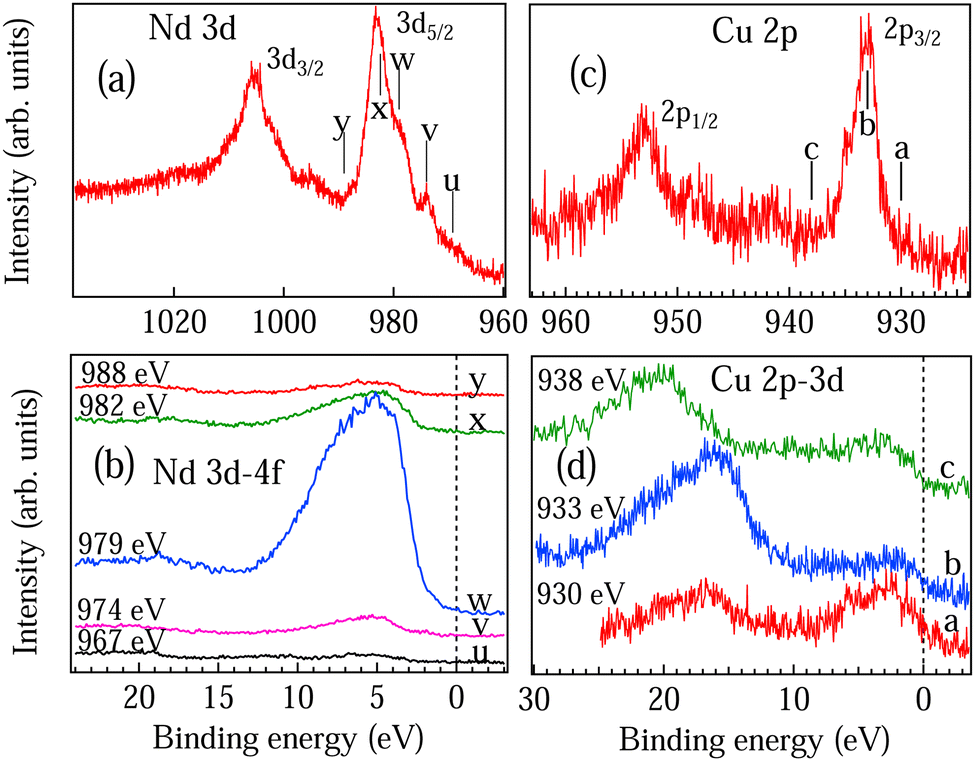 | ||
| Fig. 7 Core-levels Nd 3d and Cu 2p measured at 1486.6 eV photon energy are shown in (a and c). RPES data recorded across the Nd 3d–4f resonance are shown in (b) at some particular BEs marked by ticks in (a). RPES data recorded across the Cu 2p–3d resonance are shown in (d) at some particular BEs marked by ticks in (c). | ||
To understand the contribution of the bulk and the surface electronic structure for the topological properties in this system we have separately determined the partial DOSs at the surface (SDOS) and the bulk (BDOS) for Nd and Cu atoms and the results are shown in Fig. 8(a and b), respectively. Partial DOSs have been determined by subtracting the off-resonance spectrum from the on-resonance spectrum for the features obtained in the CIS spectra for Nd and Cu atoms (see Fig. 5 and 6) with all the resonance energies mentioned in Fig. 8(a and b). SDOSs obtained from Nd 4d–4f and Cu 3p–3d resonances are shown in the top panel of Fig. 8(a and b) while BDOSs obtained from Nd 3d–4f and Cu 2p–3d resonances are shown in the bottom panel of Fig. 8(a and b). The SDOS and BDOS of Nd atoms in Fig. 8(a) clearly show that the surface has a contribution from both the Nd3+ and Nd2+ states. The features obtained by subtracting the off-resonance spectra at 120 eV with the on-resonance spectra at 130 eV and 134 eV has the dominating Nd3+ contribution with 4fn initial state while the features obtained by subtracting the off-resonance spectra at 120 eV with the on-resonance spectra at 122 eV have the contribution due to the Nd2+ states and the 4fn+1 initial state. On the other hand, the bulk resonance shows the dominance of Nd3+ state which is hybridized with the other valence electrons. In Fig. 8(b) we find that the SDOS and BDOS of Cu are totally different. Near the EF up to 2 eV the bulk states have enhanced density as compared to the surface states. The Cu 3d states of both the bulk and surface show hybridization above 2 eV. Hence, the enhancement in the density of states around 1 eV in Fig. 4(b) is mainly due to the Cu 3d bulk states which are hybridized with the Nd2+ surface states.
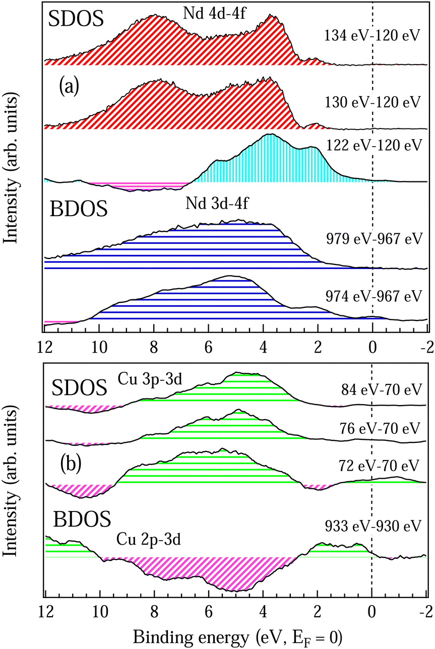 | ||
| Fig. 8 SDOS and BDOS are surface and bulk sensitive partial DOSs obtained by subtracting the off-resonance spectra from the on-resonance spectra as in Fig. 5 and 6 for Nd 4f states shown in (a) and for Cu 3d states shown in (b). On-resonance and off-resonance photon energies across Nd 4d–4f and Nd 3d–4f RPES are mentioned in (a) and across Cu 3p–3d and Cu 2p–3d RPES are mentioned in (b). | ||
In summary we find that the Nd 4f states at both the bulk and the surface have localized nature but the Cu 3d states which are hybridized with the O 2p states have delocalized character and are responsible for the charge transport. So, the electron doping in NCO by the small oxygen vacancy gives rise to the hybridization between the Cu 3d, O 2p and Nd 4f states which leads to localized polaronic states near the EF and is energetically favored on the surface. The polaron trapping energy of the Nd2+ state on the surface is found to be larger than in the bulk, which makes it energetically favorable for the polarons to travel from the bulk to the surface. Similar phenomena of polarons traveling from bulk to surface are reported in TiO2.48 The complex Cu spin orientations reported in NCO8,10,11 are associated with the polaron–polaron interaction between the Nd2+ 4f states on different atoms. The mechanism of polaron–polaron interaction in NCO can be explained like this: the decrease in structural parameter with the temperature causes the polaronic states on the surface to interact and increases the polaron hopping mechanism. This is quite evident in resistivity (Fig. 1(b)) as we find that the energy gap reduces at low temperature ∼11.3 meV; moreover, there is also enhancement in the density of states near EF (Fig. 4(b)). The thermopower measurement (Fig. 1(c)) reveals that the electron–phonon interaction is dominating above the TN while the electron–electron interaction dominates below the TN with the increase in the localization effect at low temperature. The polaron–polaron interaction at low temperature leads to the short range ferromagnetic ordering across the spin-reorientation transition. The spin polarization mainly depends on the bulk and surface interaction between the Nd3+ and Nd2+ states through the Cu–O spin cloud that leads to the enhancement of the electron density near EF (Fig. 4(a and b)). The effect of increase in electron density across the spin-reorientation transition has also been observed in the XRD peaks (Fig. 3(b)). The short range electron–lattice interaction due to the polaronic states and large negative Seebeck coefficient (−535 μV K−1 at 300 K) promises this material as an important candidate for thermoelectric applications. Moreover the localized magnetic polaron states on the surface act like a spin filter with enhanced polarized spin population making this material promising for high performance spintronic devices.
4 Conclusions
Magnetic polaronic states associated with the small oxygen deficiency have been observed in NCO. The polaronic states are mainly the Nd2+ states, which are localized within the optical energy gap. The decrease in structural parameter with temperature enhances the polaron hopping mechanism and is responsible for the charge transport in this system. The polaron-polaron interaction not only decreases the activation energy gap at low temperature but also gives rise to short range ferromagnetic ordering across the spin reorientation transitions. The interplay between electron–phonon and electron–electron interactions observed across the spin reorientation transition leads to the large negative value of the Seebeck coefficient. We find that there is distinct bulk and surface contribution in this system and the bulk–surface interaction mainly causes the spin-polarization in this system.Conflicts of interest
The authors declare that they have no known competing financial interests or personal relationships that could have appeared to influence the work reported in this paper. There are no conflicts to declare.Acknowledgements
The authors wish to thank Dr. S. V. Nakhe, Director RRCAT, and Dr. Tapas Ganguli, Head SUS, RRCAT, for their constant encouragement and support. Mr. Kiran Bariak and Ms. Madhusmita Baral of BL-10, Indus-2, RRCAT are thanked for their assistance in the beamline operation. Dr. Ravindra Jangir of RRCAT is thanked for providing annealing facility. Dr. R. Rawat of UGC-DAE, CSR is thanked for the magnetization measurement.Notes and references
- Y. Natanzon, A. Azulay and Y. Amouyal, Isr. J. Chem., 2020, 60, 1–20 CrossRef.
- M. Lorenz, et al. , J. Phys. D: Appl. Phys., 2016, 49, 433001 CrossRef.
- L. Kornblum, Adv. Mater. Interfaces, 2019, 6, 1900480 CrossRef.
- D. P. Kumah, J. H. Ngai and L. Kornblum, Adv. Funct. Mater., 2019, 1, 1901597 Search PubMed.
- G. Ren, J. Lan, C. Zeng, Y. Liu, B. Zhan, S. Butt, Y.-H. Lin and C.-W. Nan, JOM, 2014, 67, 211, DOI:10.1007/s11837-014-1218-2.
- J. Koepsell, J. Vijayan, P. Sompet, F. Grusdt, T. A. Hilker, E. Demler, G. Salomon, I. Bloch and C. Gross, Nature, 2019, 572, 358 CrossRef CAS PubMed.
- J. Zaanen, et al. , Phys. Rev. Lett., 1985, 55, 418 CrossRef CAS.
- M. Matsuda, et al. , Phys. Rev. B, 1990, 42, 10098 CrossRef CAS.
- Y. Endoh, et al. , Phys. Rev. B, 1989, 40, 7023 CrossRef CAS.
- T. Chattopadhyay, P. J. Brown and U. Kobler, Phys. C, 1991, 177, 294 CrossRef CAS.
- S. Skanthakumar, et al. , J. Appl. Phys., 1990, 67, 4530 CrossRef CAS.
- M. Imada, et al. , Rev. Mod. Phys., 1998, 70, 1039 CrossRef CAS.
- M. Naito, Y. Krockenberger, A. Ikeda and H. Yamamoto, Phys. C, 2016, 523, 28 CrossRef CAS.
- M. Scavini, G. Chiodelli, G. Spinolo and G. Flor, Phys. C, 1994, 230, 412 CrossRef CAS.
- K. Okada, JPS Conf. Proc., 2020, 30, 011069 Search PubMed.
- M. Horio, et al. , Phys. Rev. Lett., 2018, 120, 257001 CrossRef CAS.
- Q. Liu, Q. Yao, Z. A. Kelly, C. M. Pasco, T. M. McQueen, S. Lany and A. Zunger, Phys. Rev. Lett., 2018, 121, 186402 CrossRef CAS PubMed.
- M. Scavini, et al. , Phys. C, 1995, 251, 89 CrossRef CAS.
- P. Calvani, et al. , Solid State Commun., 1994, 91, 113 CrossRef CAS.
- S. W. Jang, et al. , Sci. Rep., 2016, 6, 33397 CrossRef CAS.
- E. Baldini, et al. , Proc. Natl. Acad. Sci. U. S. A., 2020, 117, 6409 CrossRef CAS.
- M.-E. Boulanger, et al. , Nat. Commun., 2020, 11, 5325 CrossRef CAS PubMed.
- R. P. Gupta and M. Gupta, Phys. C, 1989, 160, 129 CrossRef CAS.
- M. Capone, C. Castellani and M. Grilli, Adv. Condens. Matter Phys., 2010, 920860, 1 Search PubMed.
- V. Petricek and M. Dusek, Jana2000 Crystallographic computing system, 2003 Search PubMed.
- A. Ahad and D. K. Shukla, Rev. Sci. Inst., 2019, 90, 116101 CrossRef.
- S. Banik, M. K. Chattopadhyay, S. Tripathi, R. Rawat and S. N. Jha, Sci. Rep., 2020, 10, 12030 CrossRef CAS PubMed.
- C. D. Wagner, W. M. Riggs, J. F. Moulder and L. E. Davis, Handbook of X-ray Photoelectron spectroscopy, PerkinElmer Corporation, 1979 Search PubMed.
- M. P. Seah, Surf. Interface Anal., 1989, 14, 488 CrossRef CAS ; ISO 15472:2010. Surface chemical analysis – X-ray photoelectron spectrometers – Calibration of energy scales (ISO, Geneva, 2010).
- J.-S. Zhou, J. Chan and J. B. Goodenough, Phys. Rev. B, 1993, 47, 5477 CrossRef CAS.
- P. B. Allen and J. P. Nery, Phys. Rev. B, 2017, 95, 035211 CrossRef.
- R. James, Electrical properties of La2CuO4 and Nd2CuO4 and their coexistent p-n heterojunction, University of Oslo, 2020 Search PubMed.
- R. Sachidanandam, et al. , Phys. Rev. B, 1997, 56, 260 CrossRef CAS.
- B. Christophe, First-principles calculations of the local electronic structure in undoped and doped cuprates, University of Zurich, 2005 Search PubMed.
- A. C. Durst, R. N. Bhatt and P. A. Wolff, Phys. Rev. B, 2002, 65, 235205 CrossRef.
- A. Mauger and D. L. Mills, Phys. Rev. Lett., 1984, 53, 1594 CrossRef CAS.
- S. Banik, A. Arya and A. K. Sinha, RSC Adv., 2020, 10, 24343 RSC.
- S. Banik, et al. , Sci. Rep., 2017, 7, 4120 CrossRef PubMed.
- N. P. Armitage, et al. , Phys. Rev. Lett., 2002, 88, 257001 CrossRef CAS PubMed.
- H. Gabasch, et al. , Surf. Sci., 2006, 600, 2980 CrossRef CAS.
- T. G. Avval, et al. , Surf. Sci. Spectra, 2019, 26, 014021 CrossRef.
- U. Fano, Phys. Rev., 1961, 124, 1866 CrossRef CAS.
- S. Lebegue, et al. , Phys. Rev. B, 2006, 74, 045114 CrossRef.
- S. Imada, et al. , Phys. Rev. B, 2007, 76, 153106 CrossRef.
- F. Arai, S.i. Kimura and M. Ikezawa, J. Phys. Soc. Jpn., 1998, 67, 225 CrossRef CAS.
- T. Das, R. S. Markiewicz and A. Bansil, J. Phys. Chem. Solids, 2008, 69, 2963 CrossRef CAS.
- J. He, et al. , Proc. Natl. Acad. Sci. U. S. A., 2019, 116, 3449 CrossRef CAS.
- C. D. Valentin and A. Selloni, J. Phys. Chem. Lett., 2011, 17, 2223 CrossRef.
| This journal is © The Royal Society of Chemistry 2022 |