
 Open Access Article
 This Open Access Article is licensed under a Creative Commons Attribution-Non Commercial 3.0 Unported Licence
Towards three-dimensional nanoarchitectures: highly ordered bi-layer assembly of tailored magnetic nanowire arrays via template-assisted electrodeposition†
Arturo
Galindo
 a,
José Luis
Reyes-Rodríguez
a,
Cristian
Botez
a,
Mario
Moreno
b and
Arturo
Ponce
*ab
a,
José Luis
Reyes-Rodríguez
a,
Cristian
Botez
a,
Mario
Moreno
b and
Arturo
Ponce
*ab
aDepartment of Physics and Astronomy, The University of Texas at San Antonio, San Antonio, Texas 78249, USA. E-mail: arturo.ponce@utsa.edu
bInstituto Nacional de Astrofísica, Óptica y Electrónica, Puebla 72840, Mexico
First published on 25th March 2022
Abstract
The miniaturization of magnetic components down to the nanoscale has generated significant progress in expanding magnetic nanostructures into three dimensions. However, the fabrication methods currently employed are limited by the nanopatterned area of the substrate which restrains further improvement in nanowire (NW) density and surface area(SA)-to-volume (SA![[thin space (1/6-em)]](https://www.rsc.org/images/entities/char_2009.gif) :V) ratios. Herein, template-assisted electrodeposition was employed systematically to fabricate vertical bi-layers of Ni and Co/Ni freestanding NW arrays to demonstrate full control of the NW diameter, length, and chemical composition in a layer-by-layer basis, where a high SA:V ratio of 1.4 × 10⁸ m−1 was achieved. Moreover, the magnetic properties of a Co/Ni bilayer assembly were measured. The magnetostatic interactions inhertied from the template geometry lead to an easy axis of magnetization that is perpendicular to the NW axis. In addition, the saturation magnetization from each assembled layer provides an additional contribution to the bulk magnetic anisotropy, where bi-magnetic soft/hard magnetization behavior was observed. Overall, these results demonstrate the potential to open a new path in three-dimensional nanofabrication to design highly ordered vertically assembled NW arrays for numerous applications in nanotechnology research.
:V) ratios. Herein, template-assisted electrodeposition was employed systematically to fabricate vertical bi-layers of Ni and Co/Ni freestanding NW arrays to demonstrate full control of the NW diameter, length, and chemical composition in a layer-by-layer basis, where a high SA:V ratio of 1.4 × 10⁸ m−1 was achieved. Moreover, the magnetic properties of a Co/Ni bilayer assembly were measured. The magnetostatic interactions inhertied from the template geometry lead to an easy axis of magnetization that is perpendicular to the NW axis. In addition, the saturation magnetization from each assembled layer provides an additional contribution to the bulk magnetic anisotropy, where bi-magnetic soft/hard magnetization behavior was observed. Overall, these results demonstrate the potential to open a new path in three-dimensional nanofabrication to design highly ordered vertically assembled NW arrays for numerous applications in nanotechnology research.
Introduction
A half-century ago, the use of porous templates made by anodization of aluminum (Al) appeared as a new alternative for the fabrication of large-area templates with nanometer-size features.1 This technique rapidly became the focus of interest for its simple and inexpensive applicability to the fabrication of nanostructures.2–6 Much theoretical and experimental work has been devoted to demonstrating the use of anodic aluminum oxide (AAO) nanoporous templates, in combination with electrochemical methods, to fabricate monodisperse ultra-dense arrays of nanowires,7 nanorods,8 and nanodots.9 Typically, AAO templates are prepared on Al/Si substrates following a short anodization of the previously evaporated Al thin film. However, due to the limitations from the Al thickness, quick anodizations hinder the self-ordering regime of the pores causing structural and geometrical imperfections to be introduced to the AAO template.10,11 To overcome this limitation, we used a two-step anodization process of Al foils in conjunction with a 2-polymer transfer method to assemble NW arrays on the basis of template-assisted electrodeposition. In this way, nanostructures can be fabricated on large area (cm2) conductive substrates without pre-treatment of the Al foil to produce hexagonally dense arrays of magnetic NWs with precise control of the length, diameter, and interwire distance. Accordingly, the coercive field and squareness (SQ) values of the arrays are determined by the net demagnetizing field of the template porosity, in addition to the shape and magnetocrystalline anisotropies of the individual NWs.12 In this sense, magnetic NW arrays are thought to be good candidates for information storage devices as the magnetic anisotropies and the template's geometrical parameters can tune the coercivity, SQ, and magnetization dynamics of the bulk sample.13–16 Moreover, with the increasing demand in miniaturization and the physical limitation of 2D scaling dictated by Moore's law,17–19 various applications in nanotechnology with 3D architecture have been demonstrated using top-down lithography and bottom-up self-organization.20–23 In the realm of template assisted electrodeposition, NWs such as FeCoCu NWs with modulated diameters,24 FeGa/Cu multisegmented NWs,25 and CoFe2.7/CoFe2O4 alloy core/shell NWs26 have been fabricated for their complex magnetization configurations based on vortex structures, antiferromagnetic intersegment/ferromagnetic interwire ordering, and superexchange/direct exchange interactions, respectively. However, these fabrication techniques are limited by the surface area of the planar substrate as nanopatterning inherits the area coverage from the porous templates, consequently restraining improvement in NW density and SA:V ratios for 3D memory,27 which relies on increased wire density.28 To overcome this problem, we have used (AAO) template-assisted electrodeposition to fabricate three-dimensional vertical assemblies of ultra-dense arrays of freestanding magnetic NWs where morphology, chemical composition, crystal structure, and magnetic behaviors can be tailored in a layer-by-layer basis. We demonstrate this method by fabricating two bi-layer assemblies of Ni (sample 1) and Co/Ni (sample 2) NW arrays on 3 × 15 mm2 Au/Si (100) substrates where complete and uniform coverage is achieved. The bi-layer samples show significant NW order and orientation, in addition to uniform length and diameter for each vertical layer, which simplifies their integration into devices as compared to collapsed structures or random distribution of NWs after etching of the porous template.29,30 This fabrication method provides a new way to overcome substrate area limitations and ultimately provide complex three-dimensional highly ordered periodic nanostructures31 with tunable SA:V ratios and areal densities.
Experimental
Aluminum preparation
Ultra-pure (Al) sheets (99.999%, Goodfellow) of 0.2 mm thickness were cut into 3.5 × 3.5 cm2 pieces. These pieces were ultra-sonicated for 5 min in acetone and methanol to remove organic impurities present on the Al surface and subsequently rinsed with DI water. Thereafter, the Al pieces were electrochemically polished for 10 minutes at 20 V in a solution of 3:1 ethanol:perchloric acid at 2 °C with vigorous magnetic stirring. The Al samples were used as the working electrode with an exposed area of 12.25 cm2 and a platinum mesh served as the counter electrode placed at 2.5 cm in front of the Al foil. The resulting electropolished Al was rinsed with ethanol and DI water to remove any residual acid solution on the Al surface revealing a smooth surface morphology with a mirror-like finish.
AAO membrane fabrication
AAO porous membranes of varying diameters and interpore distances were fabricated following a two-step anodization process32 where two previously electropolished Al foils were placed in separate electrochemical cells. The first and second cells contained 0.3 M oxalic and 0.3 M sulfuric acid solutions, respectively. The Al samples were initially anodized at 40 V and 25 V for 10 and 4 hours, respectively with magnetic stirring at 2 °C. Second anodizations consisted of 617 seconds (cell 1) and 366 seconds (cell 2) under identical conditions. As a result, the AAO membranes entailed nanopores of 350 nm and 550 nm in length for cells 1 and 2, respectively. The pore diameter of each membrane was increased to 81 ± 5 nm for cell 1 (oxalic acid) and 47 ± 2 nm for cell 2 (sulfuric acid) by using a 5 wt% phosphoric acid solution at 45 °C for 5 min. The interpore distance in each case is 100 nm (oxalic) and 60 nm (sulfuric). These results are in agreement with previous studies33 and are presented in ESI† Fig. S1. The nanopore density (number of pores per 1 cm2) and porosity ((total area of pores/total area of scanning electron microscopy (SEM) image) × 100%) of both samples were calculated at identical magnifications using the Image J software.34 Pore densities of 2.5 × 10¹⁰ pores cm−2 and 1.1 × 10⁹ pores cm−2 with porosities of 46% and 53% were determined for the membranes anodized in sulfuric and oxalic acids, respectively.Nanopatterning of the Au/Si substrate by AAO transfer
To utilize the AAO membrane as a template for the fabrication of NWs on a substrate, an open-pore (through-hole nanochannel) is necessary. This is obtained by removing the Al2O3 barrier at the end of the nanopore. Since the AAO membrane is brittle and highly susceptible to damage during its manipulation we applied the 2-polymer transfer method proposed by Guiliani et al.35 to provide chemical protection and mechanical strength to the nanopores through the etching of the Al2O3 barrier and the membrane transfer.Removal of native Al foil and Al2O3 barrier layer
To liberate the AAO from its native Al foil, the AAO surface was rinsed with acetone to eliminate impurities and then gently dried with N2; care should be exercised to avoid bending of the Al foil. A pipette was used to dispense an S1813 photoresist (S1813 Shipley Microposit) onto the AAO surface. The aim is to fully enclose the anodized region with the S1813 photoresist using surface tension from the pipette to develop uniform coverage. A time delay of 1 minute is necessary to allow the photoresist to permeate through the nanopores to the Al2O3 barrier layer at the base. The Al foil is then spin-coated at 5000 rpm for 1 minute and subsequently placed on a hot plate at 120 °C covered by a watch glass for 1 minute. The Al is loaded in the spin coater once more to add a second layer of poly(methyl methacrylate) (PMMA A11 MicroChem) at 5000 rpm for 1 min on the S1813 layer. Finally, an identical soft bake process is repeated to cure the PMMA A11 layer.Subsequently, the liberation of the AAO from its native Al substrate is executed (see the ESI† Fig. S2). The Al side is exposed to an etching solution of copper chloride–hydrochloric acid solution (13.6 g CuCl2·2H2O + 100 mL HCl + 400 mL H2O) for 15 min at 20 °C. As the Al oxidizes into aluminum chloride, the AAO stays afloat on the acid surface. The reduction of Cu ions (Cu2+ to Cu0) produces a slight amount of Cu to precipitate on the AAO backside, which is simply removed with tweezers. A microscope slide is immersed in the acid (below the AAO), to gently attach the buoyant AAO onto the surface of the microscope slide. The AAO is then suspended in a 5 wt% phosphoric acid solution for 1 hour at 20 °C to open the pore bottoms by etching the Al2O3 barrier layer at the base. The two-polymer protective layer prevents the acid solution from reaching the nanopore walls. Lastly, the AAO is suspended in DI water.
Transfer of AAO template
The AAO membranes (still embedded in polymers) were diced into pieces of 2.5 × 5 mm2 and transferred onto a Si substrate (3 × 6 mm2) previously coated with 150 nm of Au in a vacuum chamber using thermal evaporation. To accommodate the AAO template onto the Au/Si substrate (see the ESI† Fig. S3), the AAO membrane is placed into a beaker with DI water. Then, the substrate is submerged underneath the buoyant AAO. Once the AAO is in the desired position, the Au/Si substrate and AAO template are lifted from the water simultaneously and left to dry for 5 minutes to evaporate the water accumulated between the AAO template and the Au/Si substrate. This step is essential to promote van der Waals bonding between the AAO and the substrate.36 Lastly, the two-polymer layer is removed by dispensing acetone followed by chloroform on the AAO surface. The substrate is then gently dried with N2 resulting in a highly ordered nanopatterned area.Electrodeposition conditions
Electrodeposition of Ni and Au was carried out under chronoamperometric conditions using commercial Nickel Sulfamate RTU (Technic Inc.) (pH = 3.9), and Oro temp 24 RTU Rack (Technic Inc) (pH = 5.0) solutions, respectively. Electrodeposition of Co was conducted using a homemade solution of 0.423 M CoSO4 + 0.720 M H3BO3 (pH = 5.0). A CH Instruments 660E potentiostat was used to control the potentials applied to a system consisting of a three-electrode cell configuration with an AAO/Au/Si working electrode, a platinum mesh counter electrode, and an Ag/AgCl reference electrode (+0.304 V vs. reversible hydrogen electrode). All working potentials are given with respect to this reference electrode.Magnetic characterization
Magnetic property measurements were carried out using a Quantum Design Versa Lab vibrating sample magnetometer (VSM) equipped with a 3T magnet. Hysteresis loops were recorded at T = 50 K by varying the applied magnetic field between −1.8 T and 1.8 T. The diamagnetic contribution of the substrate (AAO/Au/Si) and the sample holder was measured and extracted from the raw magnetic data.Results and discussion
Vertical assembly of NWs with tailored radial and longitudinal dimensions
A firmly attached freestanding AAO template (anodized in sulfuric acid) was transferred onto an Au/Si substrate as seen in Fig. 1b. The assembly sequence was observed using a Hitachi S 5500 field emission SEM at 30 kV. Initially, the first layer of NWs on the Au surface was assembled by electrodepositing Ni at −0.87 V for 650 seconds. The resulting Ni NWs were 550 nm in length and 47 nm in diameter (in agreement with the parameters of the AAO anodized in sulfuric acid signifying a 100% pore filling factor) with an aspect ratio (AR) of 11.7. The deposition time was selected to overgrow the AAO and develop a thin film above the template (Fig. 1c). Subsequently, a second AAO (anodized in oxalic acid) was transferred onto the thin film (Fig. 1d) in the same approach as before; however in this case the thin film operates as the new working electrode. Under this condition, the second layer of NWs was electrodeposited at −0.87 V for 413 seconds resulting in Ni NWs of 350 nm in length and 81 nm in diameter (Fig. 1e) with an AR of 3.7. The AAO templates were removed in 1 M NaOH for 4 h at 20 °C. The successful bi-layer vertical assembly of freestanding Ni NWs with distinctive diameters, lengths, and interwire distances per layer is shown in Fig. 1f, where uniform coverage is evident throughout the substrate. As can be seen, the structure remained stable through cleaving of the Si wafer for SEM analysis. In addition, the assembled NW arrays did not collapse through the assembly process due to magnetic attraction or surface tension forces37 preserving their long-range order for high density 3D magnetic memory.38 Typically, NWs collapse with an AR greater than 5, however the nucleation of a continuous film provides structural support and overcomes the agglomeration forces preventing any NW collapse. This outcome could potentially be applied to NWs of higher AR, which typically present a greater challenge of achieving uncollapsed NW arrays.39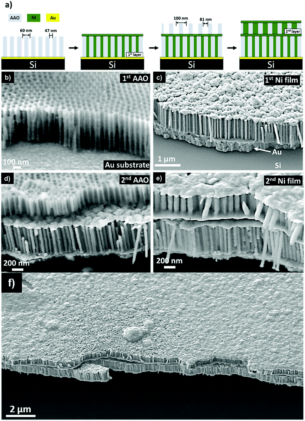 | ||
| Fig. 1 (a) Schematic illustration of the fabrication technique demonstrating the electrodeposition and transfer processes. SEM images of the assembly process of sample 1 display: (b) the cross-sectional view of the transferred AAO membrane (fabricated in sulfuric acid), (c) the resulting electrodeposited Ni nanowires (40 nm diameter & 550 nm length) with an overgrown Ni thin film, (d) the transferred AAO membrane (fabricated in oxalic acid), (e) the resulting electrodeposited Ni NWs (80 nm diameter & 350 nm length), and (f) low magnification of the final bi-layer assembly. SEM images were captured from the broken edges of the sample. | ||
Furthermore, the initial layer of Ni NWs constitutes a SA:V ratio of 8.5 × 10⁷ m−1. Consequently, through a vertical assembly of a second layer, the SA:V significantly increased to 1.4 × 10⁸ m−1 which is a notable improvement compared to those in other studies.40 This is in addition to an increase in the NW density from 2.5 × 10¹⁰ NWs cm−2 to 3.6 × 10¹⁰ NWs cm−2. Therefore this versatile assembly method can be used to fabricate NW-based electrodes for a wide range of applications41–43 that require very high SA:V ratios to enhance the electrode active area. Additionally, the complexity of the assembled nanostructures can be tuned by adjusting the template parameters and the electrochemical deposition conditions (as demonstrated in Section 3.2).
Layer-controlled chemical composition and crystal structure of assembled NWs
The chemical composition control between two assembled layers of NWs was accomplished. The assembly scheme was designed to initiate with Ni NWs in the first layer, followed by an Au thin film, and Co NWs positioned above with Au caps. Identical AAO membranes anodized in oxalic acid were used as templates during this process. The current vs. time curves for each deposition sequence is shown in Fig. 2.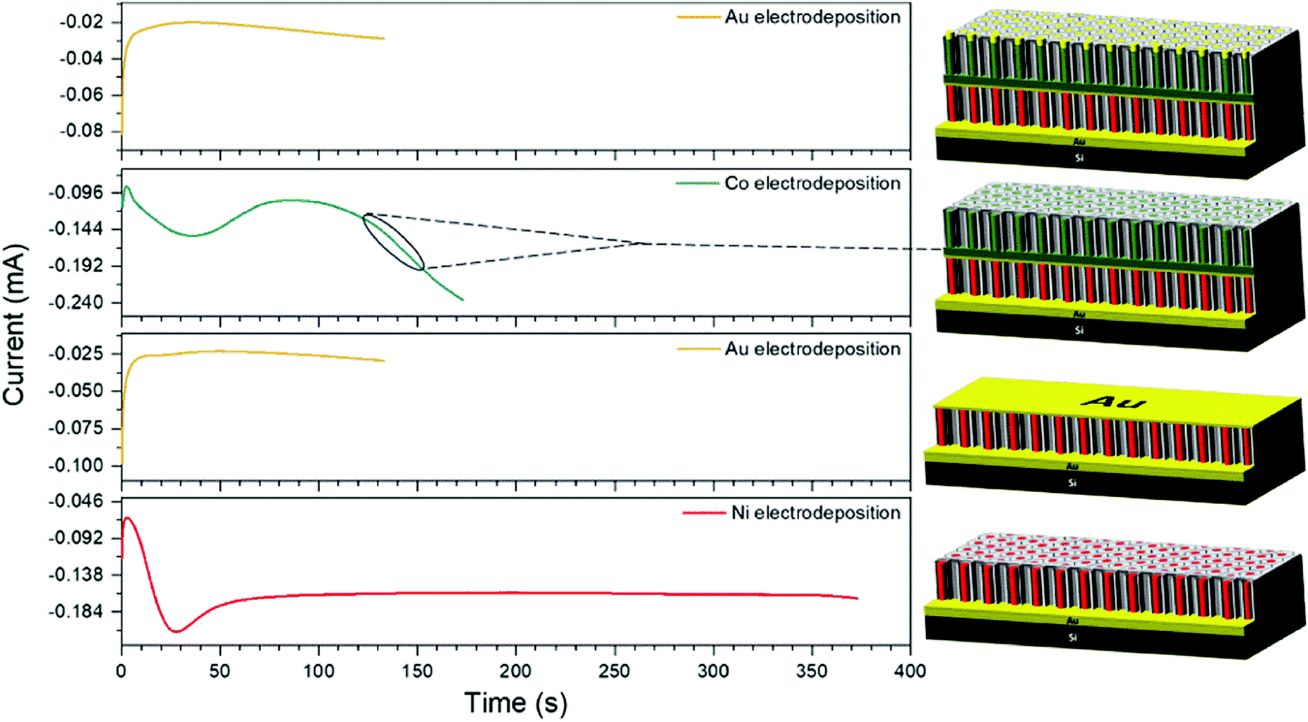 | ||
| Fig. 2 Chronoamperometric curves of Ni2+, Au3+, and Co2+ solutions in the sequential electrodeposition process under chronoamperometric conditions. The evolution of the fabrication process is illustrated for each layer assembled vertically. | ||
The first layer of NWs was fabricated by Ni electrodeposition at −0.87 V for 373 seconds. The deposition time was carefully selected to maintain the Ni confined within the nanochannel and prevent overgrowth. This can be observed by the steady-state current observed during Ni2+ reduction. This deposition process resulted in NWs of 620 nm in length (AR = 7.7). Subsequently, Au was electrodeposited on the Ni NWs using a pH = 5.5 solution at −0.85 V for 133 seconds. The Au film was used to replicate the initial deposition conditions for the first layer and to operate as the next conductive substrate. A second identical AAO template was then transferred on the electrodeposited Au film followed by the electrodeposition of Co using a pH = 5.0 solution at −0.85 V for 173 seconds resulting in Co NWs of 450 nm length (AR = 5.6). Lastly, Au caps were electrodeposited on the Co NWs at −0.85 V for 133 seconds. Overall, the completed vertical assembly after etching the AAO template is observed in Fig. 3a. The morphology of the Ni and Co NW layers was examined by making a cross-sectional cut using a FEI Scios DualBeam Focused Ion Beam (FIB) SEM with gallium ions at a beam current ranging from 7 to 30 nA. The chemical compositions between layers were determined by an energy dispersive X-ray spectrometer (EDX) attached to the FIB. The elemental map observed in Fig. 3b displays the spatial distribution of Ni, Co, and Au to be concentrated within its designated layers as originally designed. Following the assembly process a consistent porosity of 53%, a pore density of 1.1 × 10¹⁰ pores cm−2, and 100 nm interwire distance (inherited from the AAO) are evident. As identical AAO templates were used throughout the electrodeposition sequences, the lateral position of the Ni and Co NWs remained consistent as each NW is situated directly above another. Additionally, the initial layer of Ni NWs constitutes a SA:V of 5.2 × 10⁷ m−1. By assembling a second layer above, the SA:V increased to 1.3 × 10⁸ m−1 with a final NW density of 2.2 × 10⁹ NWs cm−2.
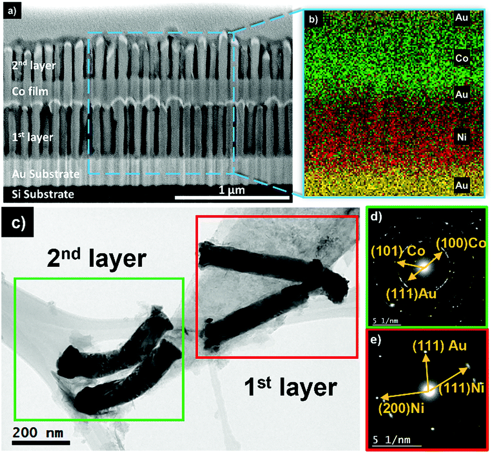 | ||
| Fig. 3 (a) SEM image of sample 2 displaying the vertical assembly of highly ordered Ni and Co NW arrays. A protective Pt layer was deposited above the second layer for FIB milling. (b) Elemental mapping overlay of Ni, Co, and Au. (c) TEM image of NWs released from the Au/Si substrate after sonication. (d and e) Electron diffraction patterns obtained from the highlighted regions in (c). | ||
Structural analysis was characterized by selected area electron diffraction (SAED) using a JEOL ARM 200F transmission electron microscope (TEM) operated at 200 kV. To acquire separation from the Au/Si substrate, sample (2) was sonicated in ethanol for 5 min. The suspended NWs were collected with the aid of an external neodymium magnet and drop-cast on a TEM grid. The region of interest shown in Fig. 3c entails two pairs of NWs that originate from the 1st and 2nd layers. Electron diffraction patterns were acquired from the respective highlighted regions as shown in Fig. 3(d and e). The top region (green) reveals polycrystalline diffraction rings in the inverse space at 0.1925 nm, 0.2199 nm, and 0.2421 nm consisting of hcp (101) & (100) Co and fcc (111) Au, respectively. The hcp phase of Co is in agreement with the electrolyte pH.44 The lower region (red) displays reflections at 0.1899 nm, 0.2169 nm, and 0.2351 nm corresponding to fcc (200) & (111) Ni crystalline phases, and fcc (111) Au, respectively. The crystal orientations of Ni are expected due to a combination of the low electrodeposition potential applied and the NW diameter of 81 nm, which satisfies the energy minimum principle.45,46 Lastly, the presence of (111) Au in both diffraction patterns appears from the evaporated substrate and the electrodeposited Au caps.
Combined magnetic behavior of a Co/Ni NW bi-layer assembly
Magnetic hysteresis loops of the assembled Co/Ni NW bi-layer (sample 2) were measured with a magnetic field applied perpendicular (⊥) and parallel (‖) to the long axis of the NWs. The bi-layer assembly has an inherent perpendicular anisotropy where strong magnetostatic coupling between neighboring NWs is evident, as the external magnetic field easily saturates the magnetic moments as seen in Fig. 4a. The close radial proximity of 15 nm establishes an antiparallel distribution of the magnetization direction within the array.13 In contrast, when the field is applied parallel to the NWs, a distinct hysteresis loop is observed where the overall contributions of the soft and hard magnetic properties of Ni and Co, respectively, are highlighted. The sheared profile and larger H‖C of 683 Oe indicates the hard-axis magnetization, due to the high magnetic field of 16 kOe (1.6 T) required to saturate the sample.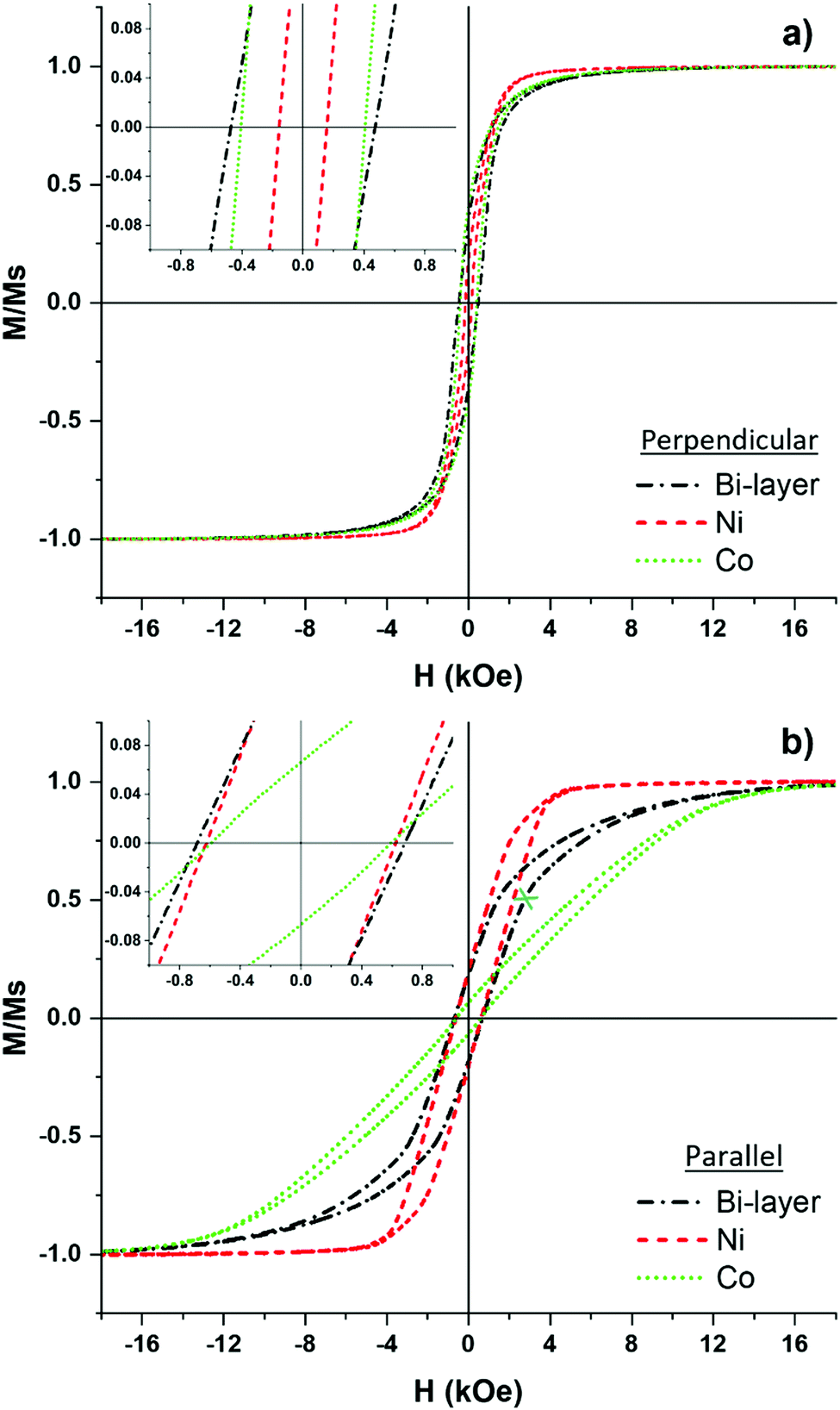 | ||
| Fig. 4 Magnetic hysteresis loops of a bi-layer assembly (Sample 2) and the individual arrays of Ni and Co NWs at 50 K measured (a) perpendicular and (b) parallel to the long axis of the NWs. The insets demonstrate a higher detail of the coercive fields. | ||
To further investigate the magnetization behavior of each layer, individual samples of Ni and Co NW arrays were measured to deconvolute the overall bi-layer magnetization. The magnetic properties of the Co/Ni bi-layer and the individual Ni and Co NW arrays are listed in Table 1.
The Co NW array shows a perpendicular anisotropy due to the low AR, magnetostatic interactions, and magnetocrystalline anisotropy. The pH of the electrolytic bath used during electrodeposition leads to a preferential alignment of the magnetic anisotropy.47,48 The combination of Co2+ ions reduced inside nanopores of 81 ± 5 nm diameter using a solution of pH = 5.0 generated the (101) and (100) hcp Co phase (verified in Fig. 3d). This pins the magnetocrystalline anisotropy direction at an angle of 45° and 90° with respect to the long axis of the NWs.49 However, due to the diameter size and high packing factor of the array, the strong magnetostatic interactions antagonize the crystalline and shape anisotropies of the individual Co NWs producing a strong macroscopic demagnetizing field oriented along the perpendicular direction. In addition, the large shape anisotropy of the Co film (130 nm height) strongly influences the overall hysteresis loop by favoring an easy magnetization axis perpendicular to the NWs (parallel to the thin film). This enhances the SQ values from 0.069 (‖) to 0.412 (⊥). In contrast, the Ni NW array displayed similar SQ values in both directions due to the low magnetocrystalline anisotropy constant of Ni (K1 = −4.5 × 10³ J m−3).50 Therefore, the (111) and (200) planes have no effect on the magnetization of the NW arrays. However, an increase in HC from 162 Oe (⊥) to 624 Oe (‖) is observed. This coercivity change is due to the greater shape anisotropy constant of the Ni NWs (KS = 7.4 × 10⁴ J m−3) and the enhanced effective shape anisotropy stemming from the longer NW length of 650 nm.
| Samples | HC (Oe) | SQ(Mr/Ms) | ||
|---|---|---|---|---|
| ‖ | ⊥ | ‖ | ⊥ | |
| Co/Ni Bi-layer | 683 | 480 | 0.184 | 0.354 |
| Ni NWs | 624 | 162 | 0.202 | 0.183 |
| Co NWs | 591 | 408 | 0.069 | 0.412 |
Altogether, the magnetic moments easily align with the external field applied in the perpendicular direction in both individual samples. Therefore, in the Ni/Co bilayer (Sample 2), we can deduce that the magnetization reversal in both layers occurs simultaneously characterized by the squared loops observed in the individual Ni and Co NWs. Conversely, with the field applied parallel to the NWs, sample (2) demonstrates two sequences of magnetizations as shown in Fig. 4b. In the initial stage of the magnetic reversal, a steep slope is observed, which is dominated by the continuous rotation and alignment of the Ni magnetic moments. Note that the hysteresis loop of the individual array of Ni NWs follows identical magnetization to that of the bi-layer assembly. Hence, once a saturation magnetization (Ms) of 484.1 emu cm−3 is reached, the magnetic moments of Ni become polarized with the external field and no additional magnetization can occur in the lower layer, thereby establishing a net magnetic field. Therefore, the gentle slope at 2700 Oe indicated by the blue “x” in Fig. 4b is a result of the ongoing polarization from the 2nd layer of Co NWs, as the magnetization slope from the bi-layer identically follows the slope from the individual sample of Co NWs. Additionally, the previously aligned magnetic moments of Ni NWs exert a dipolar stray field to the adjacent layer, thus, increasing the external field applied to the Co NWs promoting its magnetic reversal further51 until a Ms = 1422 emu cm−3 is achieved. Overall, the magnetization curve of the Co/Ni bi-layer is intermediately positioned between the loops of the individually measured samples. Therefore, bi-magnetic soft/hard magnetization measured in the parallel direction can be observed. Overall, the assembled layers of Ni and Co NWs exhibit distinct magnetization behavior determined by the variations in magnetic anisotropy, magnetostatic interactions, and Ms per layer. Ultimately, the bi-layer sample can be tailored to host distinct magnetic behaviors by adjusting the interwire separation,52 lengths,53 or chemical segmentation54 of the NWs per each assembled layer.
Conclusions
In summary, we have developed a method to fabricate vertical arrays of freestanding NWs on large area substrates (cm2) which builds upon the sequential transfer of AAO templates and electrodeposition of NWs that can be tailored layer-by-layer. Overall, this fabrication method can be implemented in several fields of nanotechnology, opening new avenues in nanofabrication to design three-dimensional textured nanostructure arrays that are not limited by the substrate area. In this regard, the fabricated Ni and Co/Ni bilayer NW array samples demonstrated remarkable uniformity in NW length, diameter, and spatial order with a complete coverage of 3 × 15 mm2 Au/Si (100) substrates where a maximum SA:V ratio of 1.4 × 10⁸ m−1 was achieved. Moreover, the magnetic hysteresis loops of the Co/Ni bilayer demonstrated an inherent perpendicular anisotropy characterized by H⊥C and SQ⊥ values of 480 Oe and 0.354, respectively and a synchronized magnetization reversal. On the other hand, when the field was applied parallel to the NWs, bi-magnetic soft/hard magnetization was observed, defined by an asynchronous magnetization reversal. The bi-layer magnetization was deconvoluted to deduce that Ni NWs (bottom layer) saturated first due to a smaller Ms (484.1 vs. 1422 emu cm−3). This occurred despite the Ni NWs having a higher H‖C (624 Oe) compared to their Co counterparts (top layer) for which H‖C is 591 Oe. Therefore, the Ms per layer provides further control of the overall magnetic anisotropy of the bi-layer sample. Consequently, this work opens new paths in the field of high-density magnetic storage by enabling the fabrication of highly ordered bi-layer NW assemblies where the magnetic properties of each layer can be tailored by varying the NW magnetostatic interactions, morphology, and chemical composition.
Author contributions
Arturo Galindo: conceptualization, methodology, formal analysis, investigation, writing – original draft, writing – review & editing, and visualization. José Luis Reyes-Rodríguez: methodology, formal analysis, investigation, writing – review & editing, and visualization. Cristian Botez: formal analysis, and writing – review & editing. Mario Moreno: writing – original draft, and writing – review & editing. Arturo Ponce: conceptualization, validation, data curation, writing – review & editing, supervision, project administration, and funding acquisition.Conflicts of interest
There are no conflicts to declare.Acknowledgements
The authors acknowledge the technical support provided during the use of the focused ion beam in the microscopy laboratory at INAOE. This work was supported by the US Department of Defense (DoD) [grant number W911NF-18-1-0439] and CONACYT [grant numbers FOMIX PUE-2018-03-02-84557, A1-S-35309].References
- H. Masuda and K. Fukuda, Science, 1995, 268, 1466–1468 CrossRef CAS PubMed.
- G. K. Singh, A. A. Golovin and I. S. Aranson, Phys. Rev. B: Condens. Matter Mater. Phys., 2006, 73, 1–12 Search PubMed.
- I. Vrublevsky, V. Parkoun, J. Schreckenbach and G. Marx, Appl. Surf. Sci., 2003, 220, 51–59 CrossRef CAS.
- T. Valand and K. E. Heusler, J. Electroanal. Chem. Interfacial Electrochem., 1983, 149, 71–82 CrossRef.
- S. K. Thamida and H. C. Chang, Chaos, 2002, 12, 240–251 CrossRef CAS PubMed.
- J. E. Houser and K. R. Hebert, J. Electrochem. Soc., 2006, 153, B566 CrossRef CAS.
- K. Kim, M. Kim and S. M. Cho, Mater. Chem. Phys., 2006, 96, 278–282 CrossRef CAS.
- Z. Huang, G. Meng, Q. Huang, B. Chen, C. Zhu and Z. Zhang, J. Raman Spectrosc., 2013, 44, 240–246 CrossRef CAS.
- C. H. Bae, S. M. Park, S. C. Park and J. S. Ha, Nanotechnology, 2006, 17, 381–384 CrossRef CAS.
- A. J. Goszczak, H. G. Rubahn and M. Madsen, Medziagotyra, 2017, 23, 6–11 Search PubMed.
- S. A. Hevia, P. Homm, F. Guzmán, H. M. Ruiz, G. Muñoz, L. S. Caballero, M. Favre and M. Flores, Surf. Coat. Technol., 2014, 253, 161–165 CrossRef CAS.
- K. Nielsch, R. B. Wehrspohn, J. Barthel, J. Kirschner, U. Gösele, S. F. Fischer and H. Kronmüller, Appl. Phys. Lett., 2001, 79, 1360–1362 CrossRef CAS.
- M. Vázquez, K. Pirota, M. Hernández-Vélez, V. M. Prida, D. Navas, R. Sanz, F. Batallán and J. Velázquez, J. Appl. Phys., 2004, 95, 6642–6644 CrossRef.
- Y. P. Ivanov, D. G. Trabada, A. Chuvilin, J. Kosel, O. Chubykalo-Fesenko and M. Vázquez, Nanotechnology, 2014, 25, 475702 CrossRef PubMed.
- S. Dellis, A. Christoulaki, N. Spiliopoulos, D. L. Anastassopoulos and A. A. Vradis, J. Appl. Phys., 2013, 114, 1–6 CrossRef.
- F. Meneses, C. Bran, M. Vázquez and P. G. Bercoff, Mater. Sci. Eng., B, 2020, 261, 114669 CrossRef CAS.
- A. Javey, S. W. Nam, R. S. Friedman, H. Yan and C. M. Lieber, Nano Lett., 2007, 7, 773–777 CrossRef CAS PubMed.
- M. M. Shulaker, G. Hills, R. S. Park, R. T. Howe, K. Saraswat, H. S. P. Wong and S. Mitra, Nature, 2017, 547, 74–78 CrossRef CAS PubMed.
- Y. Liu, S. Wang, H. Liu and L. M. Peng, Nat. Commun., 2017, 8, 1–8 CrossRef.
- S. Daryadel, A. Behroozfar, S. R. Morsali, S. Moreno, M. Baniasadi, J. Bykova, R. A. Bernal and M. Minary-Jolandan, Nano Lett., 2018, 18, 208–214 CrossRef CAS PubMed.
- F. Chen, J. Li, F. Yu, D. Zhao, F. Wang, Y. Chen, R. W. Peng and M. Wang, Adv. Mater., 2016, 28, 7193–7199 CrossRef CAS PubMed.
- C. C. J. Alcântara, F. C. Landers, S. Kim, C. De Marco, D. Ahmed, B. J. Nelson and S. Pané, Nat. Commun., 2020, 11, 1–8 CrossRef PubMed.
- F. Chen, Z. Yang, J. N. Li, F. Jia, F. Wang, D. Zhao, R. W. Peng and M. Wang, Sci. Adv., 2022, 8, 1–8 Search PubMed.
- L. A. Rodríguez, C. Bran, D. Reyes, E. Berganza, M. Vázquez, C. Gatel, E. Snoeck and A. Asenjo, ACS Nano, 2016, 10, 9669–9678 CrossRef PubMed.
- E. Ortega, S. M. Reddy, I. Betancourt, S. Roughani, B. J. H. Stadler and A. Ponce, J. Mater. Chem. C, 2017, 5, 7546–7552 RSC.
- C. L. Londoño-Calderón, O. Moscoso-Londoño, D. Muraca, L. Arzuza, P. Carvalho, K. R. Pirota, M. Knobel, L. G. Pampillo and R. Martínez-García, Nanotechnology, 2017, 28, 245605 CrossRef PubMed.
- A. Fernández-Pacheco, R. Streubel, O. Fruchart, R. Hertel, P. Fischer and R. P. Cowburn, Nat. Commun., 2017, 8, 1–14 CrossRef PubMed.
- T. Shimizu, K. Aoki, Y. Tanaka, T. Terui and S. Shingubara, Jpn. J. Appl. Phys., 2011, 50, 4–7 CrossRef.
- J. Zhang, G. A. Jones, T. H. Shen, S. E. Donnelly and G. Li, J. Appl. Phys., 2007, 101, 054310 CrossRef.
- J. Zhang, S. Agramunt-Puig, N. Del-Valle, C. Navau, M. D. Baró, S. Estradé, F. Peiró, S. Pané, B. J. Nelson, A. Sanchez, J. Nogués, E. Pellicer and J. Sort, ACS Appl. Mater. Interfaces, 2016, 8, 4109–4117 CrossRef CAS PubMed.
- C.-H. Chang, L. Tian, W. R. Hesse, H. Gao, H. J. Choi, J.-G. Kim, M. Siddiqui and G. Barbastathis, Nano Lett., 2011, 11, 2533–2537 CrossRef CAS PubMed.
- H. Masuda, J. Electrochem. Soc., 1997, 144, L127 CrossRef CAS.
- A. P. Li, F. Müller, A. Bimer, K. Nielsch and U. Gösele, J. Appl. Phys., 1998, 84, 6023–6026 CrossRef CAS.
- C. A. Schneider, W. S. Rasband and K. W. Eliceiri, Nat. Methods, 2012, 9, 671–675 CrossRef CAS PubMed.
- J. Guiliani, J. Cadena and C. Monton, Nanotechnology, 2018, 29, 075301 CrossRef PubMed.
- Y. Lei, W. Cai and G. Wilde, Prog. Mater. Sci., 2007, 52, 465–539 CrossRef CAS.
- A. M. Mebed, A. M. Abd-Elnaiem and N. M. Al-Hosiny, Appl. Phys. A: Mater. Sci. Process., 2016, 122, 1–9 CrossRef CAS.
- J. Um, M. R. Zamani Kouhpanji, S. Liu, Z. Nemati Porshokouh, S. Y. Sung, J. Kosel and B. Stadler, IEEE Trans. Magn., 2020, 56, 2–7 Search PubMed.
- C. Neetzel, H. Kamimura, M. Hayashida and T. Ohgai, Results Phys., 2019, 15, 102653 CrossRef.
- D. A. Gilbert, E. C. Burks, S. V. Ushakov, P. Abellan, I. Arslan, T. E. Felter, A. Navrotsky and K. Liu, Chem. Mater., 2017, 29, 9814–9818 CrossRef CAS.
- P. Mostafalu and S. Sonkusale, RSC Adv., 2015, 5, 8680–8687 RSC.
- S. P. Zankowski, D. Chaykina and P. M. Vereecken, J. Mater. Chem. A, 2020, 8, 14178–14189 RSC.
- S. P. Zankowski and P. M. Vereecken, ACS Appl. Mater. Interfaces, 2018, 10, 44634–44644 CrossRef CAS PubMed.
- L. G. Vivas, J. Escrig, D. G. Trabada, G. A. Badini-Confalonieri and M. Vázquez, Appl. Phys. Lett., 2012, 100, 252405 CrossRef.
- A. Cortés, G. Riveras, J. L. Palma, J. C. Denardin, R. E. Marotti, E. A. Dalchiele and H. Gomez, J. Nanosci. Nanotechnol., 2009, 9, 1992–2000 CrossRef PubMed.
- X. W. Wang, G. T. Fei, X. J. Xu, Z. Jin and L. De Zhang, J. Phys. Chem. B, 2005, 109, 24326–24330 CrossRef CAS PubMed.
- Y. Ren, Q. F. Liu, S. L. Li, J. B. Wang and X. H. Han, J. Magn. Magn. Mater., 2009, 321, 226–230 CrossRef CAS.
- G. J. Strijkers, J. H. J. Dalderop, M. A. A. Broeksteeg, H. J. M. Swagten and W. J. M. De Jonge, J. Appl. Phys., 1999, 86, 5141–5145 CrossRef CAS.
- N. Zafar, S. Shamaila, R. Sharif, H. Wali, S. Naseem, S. Riaz and M. Khaleeq-Ur-Rahman, J. Magn. Magn. Mater., 2015, 377, 215–219 CrossRef CAS.
- K. M. Razeeb, F. M. F. Rhen and S. Roy, J. Appl. Phys., 2009, 105, 083922 CrossRef.
- J. Zhang, S. Pané, J. Sort and E. Pellicer, Adv. Mater. Interfaces, 2016, 3, 1–8 CAS.
- S. K. Arora and I. V. Shvets, Mater. Today: Proc., 2020, 21, 2053–2058 CAS.
- M. Susano, M. P. Proenca, S. Moraes, C. T. Sousa and J. P. Arajo, Nanotechnology, 2016, 27, 335301 CrossRef CAS PubMed.
- B. Jang, E. Pellicer, M. Guerrero, X. Chen, H. Choi, B. J. Nelson, J. Sort and S. Pané, ACS Appl. Mater. Interfaces, 2014, 6, 14583–14589 CrossRef CAS PubMed.
Footnote |
| † Electronic supplementary information (ESI) available: SEM image of sulfuric and oxalic AAO membranes, in addition to experimental details of removal of the Al2O3 barrier layer and transfer of the AAO template. See DOI: 10.1039/d2ma00268j |
| This journal is © The Royal Society of Chemistry 2022 |