
 Open Access Article
 This Open Access Article is licensed under a
 Creative Commons Attribution 3.0 Unported Licence
Tuning the optical properties of monolayer WS2 for near-infrared-II photothermal therapy: a first-principles study
Athan
Zhang
 and
Xuan
Luo
and
Xuan
Luo
National Graphene Research and Development Center, Springfield, Virginia 22151, USA
First published on 31st May 2022
Abstract
Photothermal therapy (PTT) is a new therapeutic cancer treatment strategy that offers many advantages over traditional cancer treatments, such as minimal invasiveness, higher specificity, and precise temporal selectivity. Optical imaging in the second near-infrared region (NIR-II, 1000-1350 nm) has prospective applications in PTT and is superior to that in the first near-infrared region (650–1000 nm). However, it proves challenging to find NIR-II materials. To resolve this, several elements were tested via substitutional doping to tune the bandgap of monolayer tungsten disulfide (WS2). Two-dimensional materials have long been proved to offer various properties, with WS2 predicted to have ideal adjustable optical properties. Density functional theory calculations revealed the band structure and optical spectra of the differently doped monolayer WS2. The bandgap of monolayer WS2 was successfully tailored to activate absorption in the NIR-II region. The results show that zirconium doped WS2 had a bandgap of 0.04 eV and titanium doped WS2 had a bandgap of 0.06 eV, which was ideal for NIR-II. Doping with zirconium or titanium exhibits strong absorption in the NIR-II range with absorption coefficients of 18![[thin space (1/6-em)]](https://www.rsc.org/images/entities/char_2009.gif) 830 and 13314 cm−1, respectively, which is very competitive for PTT. This demonstrates the potential of these materials as NIR-II photothermal agents.
830 and 13314 cm−1, respectively, which is very competitive for PTT. This demonstrates the potential of these materials as NIR-II photothermal agents.
1 Introduction
Pioneering cancer research and treatment have been carried out for decades, yet cancer metastasis stands as one of the most critical challenges in the medical field and is a primary cause of cancer mortality.1 Currently, one in three women and one in two men in the United States develop cancer in their lifetime; however, a reliable cure is yet to be found for multiple forms of cancer.2 Metastasis is a complex multi-step process in which cancer cells from a primary tumor colonize distant secondary sites.3 Treatments for metastasis have been developed since its discovery. One such treatment is surgery, which proves to be ineffective, highly invasive, and causes psychological and physical distress.4–6 Other treatments, such as chemotherapy,7 radiotherapy,8 or immunotherapy,9 often result in damage to healthy tissues near the targeted tumor or side effects that may permanently change the body.4,10–12 One treatment offers the promise of a solution to those problems. Photothermal therapy (PTT) is an emerging and prospective therapeutic strategy for targeted cancer treatment that offers many advantages over traditional treatments and has attracted much attention recently.13Photothermal therapy induces cancer cell death through hyperthermia and employs near-infrared (NIR) laser irradiation to excite photoabsorbers previously dispatched to designated tumor sites.14 These photoabsorbers are often nanoparticles smaller than 50 nm in width which are inserted into the bloodstream and reach the tumor site through passive or active targeting.15 The photoabsorbers convert the photonic energy from the NIR radiation into heat, leading to the ablation of the tumor cells.16 Tumors are destroyed because of their reduced heat tolerance compared to normal tissue due to their poor blood supply.17 It is common for the intracellular temperature of cancer cells to reach above 50 degrees Celsius, resulting in necrosis and rapid cell death.18 Photothermal therapy exhibits high specificity, minimal invasiveness, and precise temporal selectivity.14 This method can be used to suppress and eradicate tumor cells while keeping the nearby tissues largely unaffected. Moreover, photothermal therapy can be combined with other cancer treatments to guarantee and further the effectiveness of metastatic tumor treatment.19
Photothermal therapy in the second near-infrared biological window (NIR-II, 1000–1350 nm)20 shows a significant advantage over that in the first near-infrared biological window (NIR-I, 650–1000 nm)20 in terms of maximum permissible exposure (MPE), penetration depth, and reduced tissue scattering.21–23 This allows treatment of tumors that may be larger or deeper inside the body. Despite this, photothermal conversion nanoagents for NIR-II have been rarely developed and reported, making finding new NIR-II materials a crucial and pressing task.24 To be an effective photothermal agent, a nanomaterial must be able to absorb light in the NIR-II region and convert the light energy into heat, otherwise known as photothermal conversion efficiency (PCE).25,26 The key to improving the photothermal therapy is selecting ideal photosensitive agents that can absorb the ideal radiation wavelength and have enhanced absorption efficiency.27
Since the groundbreaking discovery of graphene and the subsequent Nobel prize,28 novel two-dimensional nanomaterials have gained increasing interest for their potential applications in various fields, including photothermal therapy, because of their distinct electrical and optical properties.29 2D materials differ in these properties from their bulk form due to the confinement of electrons but also due to the absence of inter-layer interactions, which, despite being very weak, play an important role in determining the band structure.30 This allows 2D materials to have clear advantages in bandgap modulation. Transition Metal Dichalcogenides (TMDCs) are a class of 2D materials, similar to graphene, with the formula MX2, where M is a transition metal element (typically from Group IV to Group X) and X is a chalcogen.31,32 The family has been hypothesized to comprise semiconductors, and a few have already been experimentally found to be such.31 WS2 is a semiconducting material within the family of TMDCs with a tunable bandgap and has been tested in various optical uses and shows promise for being a good photothermal agent.33,34 WS2 possesses high carrier dynamics, high third-order nonlinear susceptibility, and broadband light absorption.35 Moreover, the theoretical models predict that WS2 has the highest carrier mobility among the semiconducting TMDCs due to better ballistic performance.36 Because of the weak interactions between layers and strong interactions within the layers of bulk WS2, ultra-thin crystals can be achieved via efficient exfoliation.37 This monolayer WS2 has a direct bandgap with extraordinary optical properties and different properties from its bulk form.38,39 Despite the promising properties, there have been fewer theoretical studies on WS2 compared to its counterpart TMDC materials. In this study, we theoretically study the electronic structure and optical properties of monolayer WS2. Doping is implemented to tune the electronic and optical properties of WS2 for NIR-II photothermal therapy and has been previously used for changing the optical properties of other materials used in photothermal therapy.40–42 Through testing of different dopant agents, we successfully tailored the bandgap structure of monolayer WS2 and activated its absorption in the NIR-II region.
Our first-principles calculations, based on the density functional theory (DFT) method, are discussed in Section 2, while the results of this study are reported and discussed in Section 3. Finally, Section 4 includes an analysis of the impact of these findings, along with a concluding statement.
2 Methods
2.1 Computational details
We performed first-principles calculations based on Density Functional Theory (DFT) using the Generalized Gradient Approximation (GGA) exchange-correlation in the Perdew–Burke–Ernzerhof (PBE)43 format implemented in the ABINIT44,45 code. We use the Projected Augmented Wave (PAW) pseudopotentials46 with projectors generated using the ATOMPAW code.47,48 The electronic structure and radius cutoff of the PAW pseudopotentials are shown in Table 1.| Element | Electron structure | Radial cutoff (bohr) |
|---|---|---|
| W | [Kr4d104f14] 5s25p66s25d4 |
2.41 |
| S | [Ne] 3s23p4 | 1.92 |
| C | [He] 2s22p2 | 1.51 |
| N | [He] 2s22p3 | 1.20 |
| O | [He] 2s22p4 | 1.42 |
| F | [He] 2s22p5 | 1.41 |
| Si | [Ne] 3s23p2 | 1.91 |
| P | [Ne] 3s23p3 | 1.91 |
| Sc | [Ne] 3s23p64s23d1 | 2.43 |
| Ti | [Ne] 3s23p64s13d3 | 2.30 |
| V | [Ne] 3s23p64s23d3 | 2.20 |
| Mn | [Ne] 3s23p64s13d6 | 2.18 |
| Se | [Ar3d10] 4s24p4 |
2.20 |
| Zr | [Ar3d10] 4s24p65s14d3 |
2.21 |
| Nb | [Ar3d10] 4s24p65s14d4 |
2.21 |
| Mo | [Ar3d10] 4s24p65s14d5 |
2.20 |
| Au | [Xe4f14] 6s1 5d10 |
2.50 |
In total energy calculations, self-consistent cycles were recognised when the total energy difference was less than 1.0 × 10⁻¹⁰ Hartree twice consecutively. The kinetic energy cutoff, the density of the Monkhorst–Pack grid, and vacuum height of the unit cell were converged until the difference between successive datasets reached a tolerance criterion of 1.0 × 10⁻⁴ Hartree, which equates to nearly 2.72 meV.
The Broyden–Fletcher–Goldfarb–Shanno (BFGS) minimization algorithm was used to perform structural optimization. The atomic structure was relaxed until the maximum atomic forces were less than 5.0 × 10⁻⁵ Hartree bohr−1.
A 2 × 2 supercell is used to calculate the doped WS2 materials. In these calculations, the kinetic energy cutoff is once again chosen to be converged until the difference between successive datasets reaches a tolerance criterion of 1.0 × 10⁻⁴ Hartree. The k-point mesh was divided by two along the lateral directions as the lattice constant was doubled and the vacuum height was reconverged. The lattice optimization was then calculated. This was applied to every dopant system.
2.2 Atomic structure
Monolayer transition metal dichalcogenides exist in different structural polytypes. TMDCs can exist in a semiconducting trigonal prismatic phase (1H) and a metallic octahedral prismatic phase (1T). A third, deformed version of the 1T phase can also be observed (1T′). The 1H form is the primary focus of this study49 since it is the most stable form as discussed later. Monolayer WS2 is composed of one layer of tungsten atoms in between two layers of sulfur atoms. The atoms of different layers are bonded with strong covalent bonds. The atomic structure of pristine 1H-WS2 can be seen in Fig. 1.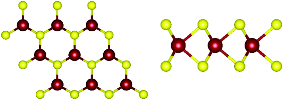 | ||
| Fig. 1 Atomic structure of WS2. (left) Top view of monolayer WS2. (right) Side view of monolayer WS2. Tungsten atoms are depicted in red and sulfur atoms are depicted in yellow. | ||
2D TMDCs have previously been doped by substitutional doping at the M (metal, W) and X (chalcogen, S) sites. It was found that doping concentrations greater than 1% were needed for changes in the electronic structure.50 For M site substitution, one of the four tungsten atoms was replaced, giving a 25% concentration. For X site substitution, one of the eight sulfur atoms were replaced, giving a 12.5% concentration.50,51 This can be seen in Fig. 2.
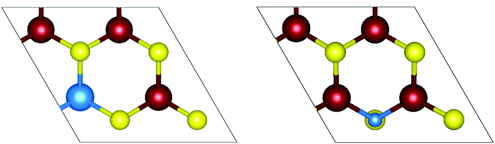 | ||
| Fig. 2 Top view of monolayer WS2 doping. (left) Tungsten substitution, M site doping, with dopant in the 2 × 2 supercell. (right) Sulfur substitution, X site doping, with dopant in the 2 × 2 supercell. Tungsten atoms are depicted in red, sulfur atoms are depicted in yellow, and the substituting dopant atom is depicted in blue. | ||
Neighboring elements are chosen to replace either the tungsten or the sulfur atom. Elements used as dopants and tested in this study are shown in Fig. 3 in a periodic table.
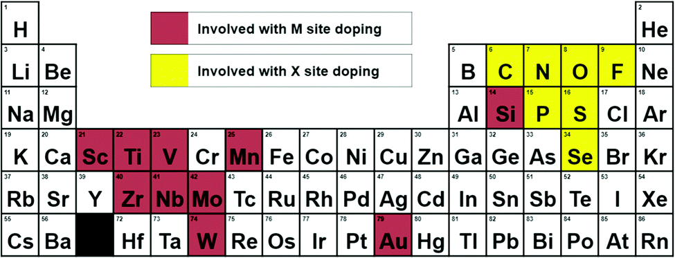 | ||
| Fig. 3 Periodic table of elements used in doping. All elements tested in this study are shown. Elements used with M site doping are colored in red, elements used with X site doping are colored in yellow. | ||
2.3 Formation energy
The total energy of the crystalline structure was calculated both with and without the dopant atom. The formation energy can then be obtained from the following equation| Eformation = EWS2+DP − EWS2 − EDP + ESB | (1) |
2.4 Electronic structure
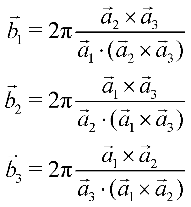
The 3D Bravais lattice is expressed by its primitive vectors (a1, a2, a3) through the following real space translational vector:![[R with combining right harpoon above (vector)]](https://www.rsc.org/images/entities/i_char_0052_20d1.gif) n = n1 n = n1![[a with combining right harpoon above (vector)]](https://www.rsc.org/images/entities/i_char_0061_20d1.gif) 1 + n22 + n33 where n1, n2, n3 ∈ Z 1 + n22 + n33 where n1, n2, n3 ∈ Z | (2) |
The corresponding reciprocal space translational vector can be expressed using
![[G with combining right harpoon above (vector)]](https://www.rsc.org/images/entities/i_char_0047_20d1.gif) m = m1 m = m1![[b with combining right harpoon above (vector)]](https://www.rsc.org/images/entities/i_char_0062_20d1.gif) 1 + m22 + m33 1 + m22 + m33 | (3) |
 | (4) |
The orbital projected band structures for WS2 and its dopant variants are calculated. A high symmetry k-point circuit  was used to sample the irreducible first Brillouin zone (IBZ) as shown in Fig. 4. We also plot the projected density of states, which show the orbital decomposition of density of states for each atom.
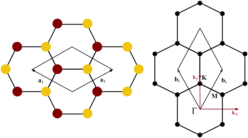 | ||
Fig. 4
K-point circuit. (left) Real space vectors of WS2. Tungsten atoms are depicted in red and sulfur atoms are depicted in yellow. (right) The reciprocal space of WS2. The k-point circuit was formed with  . . | ||
The band structures and projected density of states (PDOS) of pristine WS2 are shown in Fig. 5. It should be noted that the theoretical GGA-PBE calculations may deviate from the experimental bandgap. The Fermi level is set to 0. It shows that pristine WS2 is a clear direct semiconductor with a direct bandgap of 1.81 eV at the K symmetry point. The tungsten d-orbitals contribute the most to all bands. The eigenvalues at the Γ symmetry point are comparable in value to those at the K symmetry point, showing the potential that WS2 may become a K–Γ indirect semiconductor with defect changes. This bandgap and band structure agrees with other research, which reinforces our calculation methodology and verifies our work with previous calculations.37,52
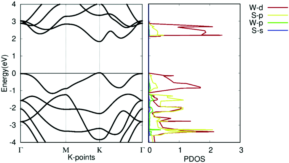 | ||
| Fig. 5 Electronic structure of pristine WS2. (left) Band structure of pristine WS2. (right) Projected density of states of pristine WS2. | ||
2.5 Optical calculations
The photonic energy of light can be calculated by the following equation: | (5) |
| α(E < Egap) = 0 | (6) |
 | (7) |
Dopants that met the bandgap requirement had their optical spectra calculated. For this, the Kohn–Sham band structure is further corrected using GW quasiparticle calculations to determine a corrected bandgap. Bethe–Salpeter equations (BSE) from the ABINIT software are used to calculate the macroscopic dielectric constants, using a scissor operator which shifts both conduction bands. Using the Many-Body Perturbation Theory (MBPT), Bethe–Salpeter equations take into account electron–hole interactions and provide a much more accurate calculation, especially in the low energy ranges.54 A standard excitonic calculation within the Tamm–Dancoff approximation (TDA) using the Haydock iterative technique was used. The calculation included local-field effects and used an automatically calculated Coulomb term evaluated using truly non-local screening W(r, r′).
The macroscopic dielectric function, εLFM(ω), is directly related to the inverse of the first element of the inverse of the microscopic dielectric matrix by means of
 | (8) |
The optical absorption spectrum is simply given by the imaginary part of εLFM(ω). The imaginary part is called ε2. Note that this equation takes into account local fields, which makes it more accurate.
The imaginary dielectric constant is calculated with the equation:
 | (9) |
The iterative Haydock technique was stopped when the difference between two consecutive evaluations of the optical spectra became less than 0.05 eV. The screening was formatted with an unsymmetrical k-mesh (shifted along the primitive axis by 0.11, 0.21, and 0.31). The imaginary dielectric constant was plotted against light intensities from 0 to 3 eV at intervals of 0.02 eV. The absorption coefficient is plotted against wavelengths ranging from 700 to 1700 nm. Both the real and imaginary dielectric constants, ε1 and ε2 were calculated. They are related to the refractive index n and extinction coefficient κ through the equations
| ε1 = n2 − κ2 | (10) |
| ε2 = 2nk | (11) |
The absorption coefficient can then be calculated with respect to κ:
 | (12) |
The optical properties of WS2 are shown in Fig. 6. Due to the high bandgap of pristine WS2, it has very low absorption in ranges below its bandgap. It shows a minor peak at 2.5 eV in the imaginary part of the complex dielectric function. It appears to have no peak in the absorption spectrum, with the maxima being below 700nm. These results appear to be similar to other studies.55 This shows that pristine WS2 is clearly not ideal for NIR-II applications. Thus, it is necessary to engineer the optical properties of WS2.
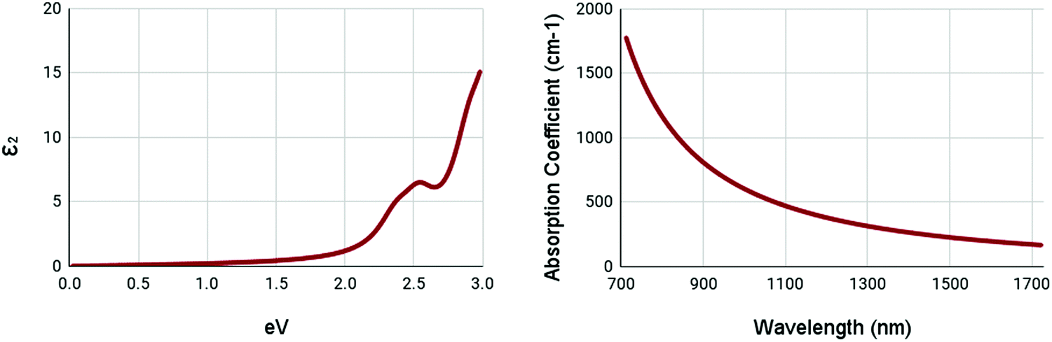 | ||
| Fig. 6 Optical spectra of pristine WS2. (left) Imaginary dielectric constant, ε2 of pristine WS2. (right) Absorption coefficient of pristine WS2. | ||
3 Results and discussion
3.1 Atomic structure and doping
WS2 in its monolayer trigonal prismatic (1H) form was tested. The crystal was in a hexagonal structure with the space group P6(3)/mmc.37 While WS2 technically exists in the 1H, 1T, and 1T′ phases, there is still controversy regarding the electronic properties of the 1T and 1T′ phases.56 Because WS2 is a group VI TMDC, it is more likely to exist in the 1H or 2H phase.57 This is because the ground state energy of the 1T phase is 85 meV higher than that of the 1H phase. This means that the 1T phase is metastable and will turn into the 1H phase spontaneously under normal conditions.56 While it is possible to create 1T WS2 with processes such as heating and annealing treatments,58 lithium intercalation, and electron beam stimulation,57 it has never been observed in natural crystals.58The intrinsic doping behaviors of TMDCs are believed to spawn from defect formation during the fabrication process. Unfortunately, these defects are difficult to control, with reports of Fermi levels varying by up to 1 eV between regions separated by only tens of nanometers.59 Thus, efforts have been made to develop methods to reliably dope TMDCs. One promising approach is the substitutional doping of the transition metal atom, in this case, tungsten. For a given TMDC, both the conduction band minimum (CBM) and valence band maximum (VBM) belong to d-orbitals on the transition metal.60 This means that substituting with a transition metal atom possessing one more/fewer valence electron will induce n/p-type doping. If the atomic radius of the dopant is similar to that of the host, a minor strain will be put on the crystal structure, maintaining a clean and stable surface.51 Substitutional doping of the sulfur atom has also been tested for WS2, creating bond changes and altering the bandgap.61
With a 2 × 2 supercell, substitutional doping was carried out. As mentioned before, the crystal structures were atomically relaxed to ideal positions. Table 2 lists the structural parameters of M site dopants on top and the X site dopants on the bottom after being relaxed.
| Material | M–S bond length | a | c | Material | M–S bond length | a | c |
|---|---|---|---|---|---|---|---|
| Si | 4.4711 | 12.2718 | 22.3860 | Zr | 4.7812 | 12.4906 | 23.8208 |
| Sc | 4.7712 | 12.4923 | 21.7523 | Nb | 4.6524 | 12.2215 | 22.2817 |
| Ti | 4.5867 | 12.2427 | 22.3328 | Mo | 4.5721 | 12.0531 | 20.9875 |
| V | 4.8830 | 12.0653 | 22.0092 | Au | 4.8465 | 12.4760 | 22.7585 |
| Mn | 4.3822 | 12.0145 | 22.9128 |
| Material | X–W bond length | a | c | Material | X–W bond length | a | c |
|---|---|---|---|---|---|---|---|
| C | 3.8437 | 12.0647 | 21.0078 | F | 4.3797 | 11.9285 | 19.7816 |
| N | 3.8112 | 11.9616 | 20.8283 | P | 4.622 | 12.1136 | 21.0929 |
| O | 3.9412 | 11.8640 | 20.6583 | Se | 4.8158 | 12.1111 | 20.0843 |
To evaluate the thermodynamic stability of these structures, the calculation of the formation energies was carried out as from eqn (1). Table 3 lists the formation energies for all doped structures. With the exception of Si, Mn, Mo, Au, and F doping, all structures were found to have negative formation energies, showing that those materials were mechanically stable in a natural environment. The doped structures that were found to have positive formation energies are mostly of very small magnitudes.
| Material | Formation energy (eV) | Material | Formation energy (eV) |
|---|---|---|---|
| Si | 0.2912 | C | −1.5402 |
| Sc | −3.7293 | N | −2.4626 |
| Ti | −2.1470 | O | −0.5442 |
| V | −0.4327 | F | 1.5062 |
| Mn | 0.5823 | P | −1.4313 |
| Zr | −2.4998 | Se | −1.7742 |
| Nb | −2.5307 | ||
| Mo | 0.1048 | ||
| Au | 0.9433 |
3.2 Electronic structure
Substitutional doping is the most commonly used method for doping TMDCs. While other methods such as introducing surface adatoms or vacancies exist, they are more likely to cause structural and undesirable results. The substitution of the tungsten atom with Si, Sc, Ti, V, Mn, Zr, Nb, Mo, and Au was carried out at a concentration of 25%. The band structures of the different doped variations are shown in Fig. 7.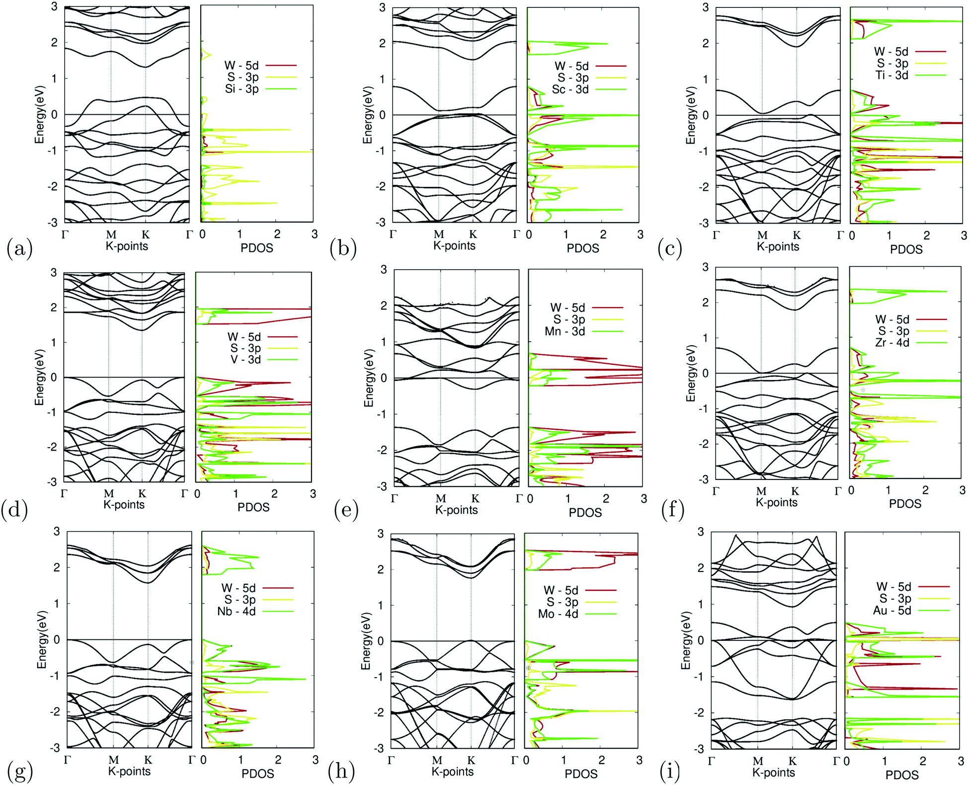 | ||
| Fig. 7 Electronic structure of M site dopants. (left) Band structure of M site dopants. (right) Projected density of states of M site dopants. | ||
Organizing the dopants by atomic order, the first dopant is silicon. Fig. 7(a) depicts the band structure and projected density of states for Si-doped WS2. It appears to show degenerate doping as the appearance of many band crossings is found near the Fermi level. An unsuccessful bonding between the Si atom and surrounding sulfur atoms was also observed, furthering this argument. The S-3p orbital appears to dominate the states near the Fermi level, as seen in the projected density of states. These failures could be caused by the difference in the atomic radii of tungsten and the Si atom, which would cause instability within the crystal.
While doping with silicon had undesirable results, doping with scandium provided the other extreme with large changes in the electronic structure. Fig. 7(b) depicts the band structure and projected density of states for Sc-doped WS2. Doping reduced the bandgap to 0.10 eV. There appears to be a less prominent defect band, with the lowest unoccupied band being closer to the occupied bands than the other unoccupied bands. Since Sc has a 3+ charge, the formation of a donor-level mid-gap band appears. The Sc-3d orbital contributes the most to the CBM. The mid-gap band seems to be equally dominated by the W-5d, S-3p, and Sc-3d orbitals, showing that possible interactions between the Sc and W, S atoms are the cause for the bandgap reduction. Because the bandgap was reduced to less than 0.92 eV, it was suitable for further calculations as shown later.
Similarly, doping with titanium showed similar results to scandium. Fig. 7(c) depicts the band structure and projected density of states for Ti-doped WS2. Doping reduced the bandgap to near metallic levels with a bandgap of 0.06 eV. It should be noted that there appears to be a defect band, with the lowest unoccupied band being closer to the occupied bands than the other unoccupied bands. Ti is a p-type dopant since tungsten has a 6+ charge while Ti has a 4+ charge. Because of this, the formation of a donor-level mid-gap band appears. The Ti-3d orbital contributes the most to the CBM. The mid-gap band seems to be equally dominated by the W-5d, S-3p, and Ti-3d orbitals, showing that possible interactions between the Ti and W, and S atoms are the cause for the bandgap reduction. Doping with Ti also met the bandgap threshold.
In contrast, doping with vanadium shows an example of successful doping but with relatively small changes to the electronic structure. Fig. 7(d) depicts the band structure and projected density of states for V-doped WS2. Doping with V appeared to result in noticeable changes in the bandgap, which narrowed down to 1.35 eV. The bandgap shifted into a K–Γ indirect bandgap as was predicted to possibly occur earlier. The W-5d orbital contributed the most to the VBM and CBM.
Doping with manganese once again shows an example of incomplete doping. Fig. 7(e) depicts the band structure and projected density of states for Mn-doped WS2. Doping with Mn appears to result in drastic changes in the bandgap, causing the material to become a semi-metal with the formation of a donor-level point at the Γ symmetry point, 0.06 meV below the Fermi level. It was found that the W-5d orbital dominated the contribution of the states around the Dirac point.
Doping with zirconium showed promising results, with attributes similar to that of doping with titanium or scandium. Fig. 7(f) depicts the band structure and projected density of states for Zr-doped WS2. Doping reduced the bandgap to near metallic levels with a bandgap of 0.03 eV. It should be noted that there appears to be a defect band, with the lowest unoccupied band being closer to the occupied bands than the other unoccupied bands. Zr is a p-type dopant since tungsten has a 6+ charge while Zr has a 4+ charge. Because of this, the formation of a donor-level mid gap band appears. The Zr-4d orbital contributes the most to the CBM. The mid-gap band seems to be equally dominated by the W-5d, S-3p, and Zr-4d orbitals, showing that possible interactions between the Zr and W, S atoms are the cause for the bandgap reduction. Doping with Zr met the bandgap threshold. It should be noted that Sc, Ti, and Zr, all reduced the bandgap significantly and had mid gap donor states, caused by their p-type doping. Given that these materials were all group III or IV, this may be a trend that continues with the rest of the groups.
Doping with niobium showed successful yet small changes to the electronic structure. Fig. 7(g) depicts the band structure and projected density of states for Nb-doped WS2. Doping with Nb appeared only to lead to minor changes in the bandgap, narrowed by 0.10 eV to a bandgap of 1.71 eV. The doping featured no major anomalies except that the bandgap was shifted into a K–Γ indirect bandgap. The Nb-4d orbital contributes largely to the CBM and VBM, giving reason to believe that the Nb doping was the cause for the bandgap change.
Additionally, doping with molybdenum also had successful yet small changes. Fig. 7(h) depicts the band structure and projected density of states for Mo-doped WS2. Doping with Mo appeared only to lead to minor changes in the bandgap, narrowed by 0.07 eV to a bandgap of 1.74 eV. The doping featured no major anomalies. The CBM is primarily dominated by the W-5d orbital while the VBM appears to be equally dominated by the W-5d, S-3p, and Mo-4d orbitals.
Finally, Fig. 7(i) depicts the band structure and projected density of states for Au-doped WS2. It appears to show degenerate doping. The appearance of many band crossings is found near the Fermi level. There appears to be a defect bandgap at the K symmetry point right above the CBM. Besides this, doping with Au appears to be largely unsuccessful. The PDOS shows that the Au-5d and S-3p orbitals seem to dominate the CBM, which gives reason to believe doping with Au to be the cause of this failure.
Out of all the materials tested for M site doping, Sc, Ti, and Zr dopants fitted the bandgap threshold being less than 0.92 eV. V, Nb, and Mo doping all had successful yet minor bandgap changes. Si, Mn, and Au doping resulted in degenerate doping.
The substitution of the sulfur atom with C, N, O, F, P, and Se was also carried out. The band structures of the different doped variations are shown in Fig. 8. Note that X site substitutional doping was carried out at a concentration of 12.5%.
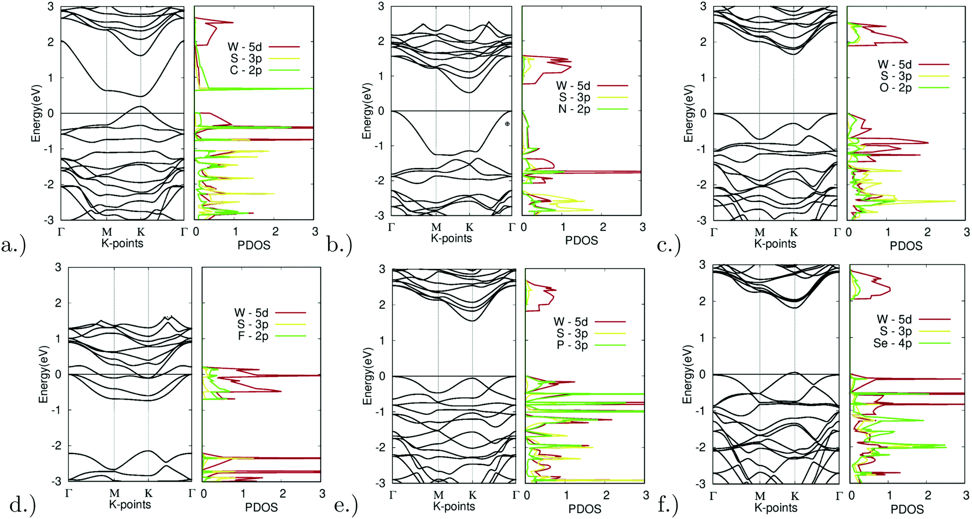 | ||
| Fig. 8 Electronic structure of X site dopants. (left) Band structure of X site dopants. (right) Projected density of states of X site dopants. | ||
Starting with doping with carbon, Fig. 8(a) depicts the band structure and projected density of states for C-doped WS2. Doping with C resulted in a direct bandgap of 0.28 eV at the K symmetry point. The lowest unoccupied band dips far below that of the other unoccupied bands. The C-2p orbital largely dominates the lowest point of this band. Extra holes moved up to higher energy levels, thus shrinking the bandgap. The top valence band was dominated by the C-2p and W-5d orbitals, a sign of hybridization. This indicates that an emerging bond between the W and C atoms is the main reason for the bandgap reduction. This can be further confirmed by the relatively short bond length absorbed, as seen in Table 2 mentioned earlier, with a bond length of 3.8437 bohr being the second shortest bond length observed out of all the X site dopants.
As another promising result, doping with nitrogen also showed ideal electronic properties. Fig. 8(b) depicts the band structure and projected density of states for N-doped WS2. Doping with C resulted in an indirect K–Γ bandgap of 0.53 eV. The top valence band was dominated by the N-2p and W-5d orbitals, once again a sign of hybridization. This indicates that an emerging bond between the W and N atoms is the main reason for the bandgap reduction. This can be further confirmed by the relatively short bond length absorbed, as seen in Table 2 mentioned earlier, with a bond length of 3.8112 bohr being the shortest bond length observed out of all the X site dopants.
With successful yet small changes in the electronic structure, Fig. 8(c) depicts the band structure and projected density of states for O-doped WS2. Doping with O had only minor changes with a K–Γ indirect bandgap of 1.66 eV. The W-5d orbital contributed the most to the CBM and VBM.
The only example of failed doping was seen for fluorine doping. Fig. 8(d) depicts the band structure and projected density of states for F-doped WS2. Doping with F appeared to be largely unsuccessful, resulting in degenerate doping and the formation of a metal. This was likely due to the high doping concentration. The density of states also shows missing states above 0 eV. This could be due to the extremely high electronegativity that fluorine possesses.
Minor changes were once again observed in phosphorus doping. Fig. 8(e) depicts the band structure and projected density of states for P-doped WS2. Doping with P led to only minor changes with a K–Γ indirect bandgap of 1.56 eV. The W-5d orbital contributed largely to the unoccupied bands, yet both the P-3p and W-5d orbitals contributed equally to the occupied bands.
Finally, Fig. 8(f) depicts the band structure and projected density of states for Se-doped WS2. Doping with Se led to only minor changes with a direct bandgap of 1.76 eV at the K symmetry point. The W-5d orbital contributed the most to the CBM and VBM.
Out of all materials tested for X site doping, only the C and N dopants fitted the bandgap threshold of being less than 0.92 eV. O, P, and Se all had successful yet minor bandgap changes. F resulted in degenerate doping.
3.3 Optical spectra
The optical spectra were then calculated for materials whose bandgap met the threshold requirement of a bandgap less than 0.92 eV. The bandgap, scissor operator, wavelength of peak absorption coefficient within the NIR-II range, and absorption coefficient of the said peak, are listed. This is found in Table 4 with M site dopants on top and X site dopants at the bottom.| Material | Bandgap (eV) | Scissor operator (eV) | λ (nm) | α (cm−1) |
|---|---|---|---|---|
| Si | 0.00 | |||
| Sc | 0.10 | 0.18 | 1016 | 9119 |
| Ti | 0.06 | 0.05 | 1350 | 13314 |
| V | 1.35 | |||
| Mn | 0.00 | |||
| Zr | 0.04 | 0.14 | 1347 | 18830 |
| Nb | 1.71 | |||
| Mo | 1.74 | |||
| Au | 0.00 | |||
| C | 0.28 | -0.07 | 1000 | 8709 |
| N | 0.53 | 0.72 | 1000 | 870 |
| O | 1.66 | |||
| F | 0.00 | |||
| P | 1.56 | |||
| Se | 1.76 | |||
The optical spectra of the M site dopants which qualified for further calculations can be found in Fig. 9. It is apparent that all three materials – Ti, Zr, and Sc – had peaks at around 0.3–0.4 eV for the imaginary dielectric constant. Despite this similarity, they have very different absorption coefficients. Both Ti and Zr share similar shapes within the absorption graph with a gradual increase of the absorption coefficient after 900 nm. Overall, the absorption coefficient of Zr is higher than Ti. Sc appears to deviate from this trend with a much lower yet consistent absorption coefficient from 700–1700 nm. Sc had a maximum absorption coefficient of 9119 cm−1 at a wavelength of 1016 nm. Ti had a maximum absorption coefficient of 13314 cm−1 at 1350 nm and Zr had a maximum absorption coefficient of 18830 cm−1 at a wavelength of 1347 nm.
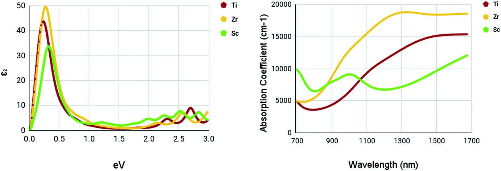 | ||
| Fig. 9 Optical spectra of M site dopants. (left) Imaginary dielectric constant, ε2 of M site dopants. (right) Absorption coefficient of M site dopants. | ||
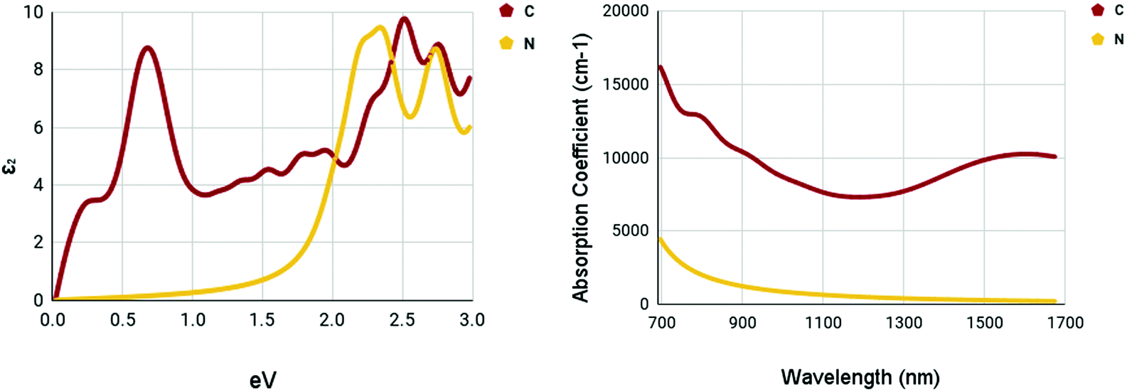
The optical spectra of the X site dopants which qualified for further calculations can be found in Fig. 10. The optical spectra of C and N appear to be very different. There appear to be two peaks at 0.7 and 2.52 eV for C in the imaginary dielectric constant. There appear to be two peaks at 2.34 and 2.76 eV for N in the imaginary dielectric constant. Both materials show widely different shapes. Despite this, the absorption coefficient spectrum was rather plain. While C has a rather moderate absorption coefficient of around 7500–10000 cm−1, N appears to be completely devoid of any strengths, despite having a rather promising bandgap.
 | ||
| Fig. 10 Optical spectra of X site dopants. (left) Imaginary dielectric constant, ε2 of X site dopants. (right) Absorption coefficient of X site dopants. | ||
It appears that the M site dopants had much higher absorption coefficients relative to the X site dopants. Among all materials that were tested, titanium and zirconium doped WS2 had the highest absorption coefficients within the NIR-II range of 1000–1350 nm, offering to be potential NIR-II photothermal agents. The other materials seemed to offer only mediocre results.
3.4 Biocompatibility and cytotoxicity
A prerequisite for all biomedical materials is biocompatibility and cytotoxicity.62 Despite existing biomedical applications using TMDCs, few investigations into the biocompatibility and toxicity have been performed.63 Nevertheless, there is still strong evidence for their safe usage. In vivo toxicology tests of fullerene-like WS2 nanoparticles on mammals showed no toxic effects.64 Cytotoxicity tests of WS2 on human cell-lines, salivary gland cells, and A549 showed that they are nontoxic to cells and had a high cell viability after prolonged exposure.65,66Additionally, because TMDCs have their chalcogens located on the exterior of the 2D layers, there are reduced interactions between cells and the interior metal which might have potentially caused damage to cells.67 TMDCs that were composed of disulfides rather than diselenides or ditelenides were also found to be less hazardous.67 Some TMDCs (MoS2, WS2, and WSe2) have also been found to have greater cell viability than graphene materials.68,69 Lastly, the cytotoxicity can be altered depending on the preparation method68 or surface modifications (such as polyethylene glycol (PEG) or doxorubicin (DOX) coating).67,70
4 Conclusions
Numerous materials have been introduced into the testing of photothermal therapy, shedding light on the potential of this emerging cancer treatment. With monolayer tungsten disulfide being the base of our nanomaterials, a range of dopant variations has been tested.Out of the fifteen dopants tested for M site and X site doping, five dopants passed the bandgap threshold of less than 0.92 eV. The dopants, Ti, Zr, Sc, C, and N, had their optical spectra and constants calculated. The X site dopants appeared to be less prosperous. X site doping with N resulted in low absorption coefficients within the NIR-II range, with values less than 1000 cm−1, proving to be a not ideal photoabsorber. X site doping with C proved to be better than N. The maximum absorption coefficient within the NIR-II range was 8709 cm−1 at a wavelength of 1000 nm.
M site doping was much more promising. Sc maintained an absorption coefficient of around 6500–9500 cm−1 in the NIR-II range with a peak at 9119 cm−1 at a wavelength of 1016 nm. Doping with Ti had higher absorption coefficients within the NIR-II range compared to Sc. The maximum absorption coefficient within the NIR-II range was 13314 cm−1 at a wavelength of 1350 nm. Zr was the most promising out of all three M site dopants. A slight peak was observed at around 1347 nm with an absorption coefficient of 18830 cm−1.
Through Density Functional Theory calculations within the Abinit computational program suite, it was found that zirconium-doped and titanium-doped monolayer tungsten disulfide could be possible ablation agents for photothermal therapy in the second near-infrared window. With peak absorption coefficients of 18830 and 13314 cm−1 in the NIR-II range for zirconium-doped and titanium-doped, respectively, they show promise as photoabsorbers. Their absorption coefficients are competitive with other current photothermal therapy materials, but specialize in the NIR-II range, a more effective and efficient form of photothermal therapy. This makes these novel materials valuable and worth carrying out more in-depth studies. Further research should be done before these materials can reach clinical use. Future work includes an analysis of the photothermal conversion efficiency and the cytotoxicity of these materials. Additional research into different concentrations and dopants is also a potential avenue of research. This study provides a valuable guideline and lays the groundwork for future fabrication and experimentation on tungsten disulfide and its dopant variants for photothermal therapy.
Data availability
The raw data required to reproduce these findings cannot be shared at this time due to technical or time limitations. The processed data required to reproduce these findings cannot be shared at this time due to technical or time limitations.Author contributions
All of the authors made important contributions to this work. Specifically, Athan Zhang conceived and designed the research procedures, carried out DFT calculations, executed data visualization, contributed to writing – original draft, and contributed to writing – review and editing. Xuan Luo aided in designing the methodology and contributed to writing – review and editing.Conflicts of interest
The authors declare that they have no known competing financial interests or personal relationships that could have appeared to influence the work reported in this paper.Acknowledgements
This research did not receive any specific grant from funding agencies in the public, commercial, or not-for-profit sectors.References
- G. P. Gupta and J. Massagué, Cancer metastasis: Building a framework, Cell, 2006, 127, 679–695 CrossRef CAS PubMed.
- R. Siegel, et al., Cancer treatment and survivorship statistics, 2012, CA: A Cancer J. Clin., 2012, 62, 220–241 Search PubMed.
- A. Schroeder, et al., Treating metastatic cancer with nanotechnology, Nat. Rev. Cancer, 2011, 12, 39–50 CrossRef PubMed.
- A. Sudhakar, History of Cancer, Ancient and Modern Treatment Methods, J. Cancer Sci. Ther., 2009, 1, i–iv CrossRef PubMed.
- C. Markopoulos, et al., Impact of breast cancer surgery on the self-esteem and sexual life of female patients, J. Int. Medi. Res., 2009, 37, 182–188 CrossRef CAS PubMed.
- G. C. Wishart, et al., PREDICT: a new UK prognostic model that predicts survival following surgery for invasive breast cancer, Breast Cancer Res., 2010, 12, R1 CrossRef PubMed.
- B. A. Chabner and T. G. Roberts, Chemotherapy and the war on cancer, Nat. Rev. Cancer, 2005, 5, 65–72 CrossRef CAS PubMed.
- R. Atun, et al., Expanding global access to radiotherapy, Lancet Oncol., 2015, 16, 1153–1186 CrossRef PubMed.
- I. Mellman, G. Coukos and G. Dranoff, Cancer immunotherapy comes of age, Nature, 2011, 480, 480–489 CrossRef CAS PubMed.
- E. Ayalew Sisay, Drug related problems in chemotherapy of cancer patients, J. Cancer Sci. Ther., 2015, 7, 55–59 Search PubMed.
- S. C. Formenti and S. Demaria, Systemic effects of local radiotherapy, Lancet Oncol., 2009, 10, 718–726 CrossRef PubMed.
- F. Kroschinsky, et al., New drugs, new toxicities: Severe side effects of modern targeted and immunotherapy of cancer and their management, Crit. Care, 2017, 21, 89 CrossRef PubMed.
- S. Nomura, et al., Highly reliable, targeted photothermal cancer therapy combined with thermal dosimetry using a near-infrared absorbent, Sci. Rep., 2020, 10, 9765 CrossRef CAS PubMed.
- L. Zou, et al., Current approaches of photothermal therapy in treating cancer metastasis with nanotherapeutics, Theranostics, 2016, 6, 762–772 CrossRef CAS PubMed.
- W. Yang, H. Liang, S. Ma, D. Wang and J. Huang, Gold nanoparticle based photothermal therapy: Development and application for effective cancer treatment, Sustainable Mater. Technol., 2019, 22, e00109 CrossRef CAS.
- A. Doughty, et al., Nanomaterial applications in photothermal therapy for cancer, Materials, 2019, 12, 779 CrossRef CAS PubMed.
- X. Huang, P. K. Jain, I. H. El-Sayed and M. A. El-Sayed, Plasmonic photothermal therapy (PPTT) using gold nanoparticles, Lasers Med. Sci., 2008, 23, 217–228 CrossRef PubMed.
- M. I. Khot, et al., A review on the scope of photothermal therapy-based nanomedicines in preclinical models of colorectal cancer, Clin. Colorectal Cancer, 2019, 18, e200–e209 CrossRef PubMed.
- J. Nam, et al., Chemo-photothermal therapy combination elicits anti-tumor immunity against advanced metastatic cancer, Nat. Commun., 2018, 9, 1074 CrossRef PubMed.
- B. Tang, et al., A supramolecular radical dimer: High-efficiency NIR-II photothermal conversion and therapy, Angew. Chem., Int. Ed., 2019, 58, 15526–15531 CrossRef CAS PubMed.
- H. Pan, et al., A cruciform phthalocyanine pentad-based NIR-II photothermal agent for highly efficient tumor ablation, Chem. Sci., 2019, 10, 8246–8252 RSC.
- Y. Liu, P. Bhattarai, Z. Dai and X. Chen, Photothermal therapy and photoacoustic imaging via nanotheranostics in fighting cancer, Chem. Soc. Rev., 2019, 48, 2053–2108 RSC.
- Z. Huang, et al., Two-dimensional MXene-based materials for photothermal therapy, Nanophotonics, 2020, 9, 2233–2249 CAS.
- X. Han, et al., Therapeutic mesopore construction on 2D Nb2C MXenes for targeted and enhanced chemo-photothermal cancer therapy in NIR-II biowindow, Theranostics, 2018, 8, 4491–4508 CrossRef CAS PubMed.
- K. Hu, et al., Marriage of black phosphorus and Cu2+ as effective photothermal agents for PET-guided combination cancer therapy, Nat. Commun., 2020, 11, 2778 CrossRef CAS PubMed.
- H. S. Jung, et al., Organic molecule-based photothermal agents: an expanding photothermal therapy universe, Chem. Soc. Rev., 2018, 47, 2280–2297 RSC.
- F. Jabeen, M. Najam-ul-Haq, R. Javeed, C. Huck and G. Bonn, Au-Nanomaterials as a superior choice for near-infrared photothermal therapy, Molecules, 2014, 19, 20580–20593 CrossRef PubMed.
- M. S. Dresselhaus and P. T. Araujo, Perspectives on the 2010 Nobel Prize in Physics for graphene, ACS Nano, 2010, 4, 6297–6302 CrossRef CAS PubMed.
- L. Wu, et al., Sensitivity enhancement by using few-layer black phosphorus-graphene/TMDCs heterostructure in surface plasmon resonance biochemical sensor, Sens. Actuators, B, 2017, 249, 542–548 CrossRef CAS.
- R. Mas-Balleste, C. Gomez-Navarro, J. Gomez-Herrero and F. Zamora, 2D materials: To graphene and beyond, Nanoscale, 2011, 3, 20–30 RSC.
- D. Jariwala, V. K. Sangwan, L. J. Lauhon, T. J. Marks and M. C. Hersam, Emerging device applications for semiconducting two-dimensional transition metal dichalcogenides, ACS Nano, 2014, 8, 1102–1120 CrossRef CAS PubMed.
- Q. H. Wang, K. Kalantar-Zadeh, A. Kis, J. N. Coleman and M. S. Strano, Electronics and optoelectronics of two-dimensional transition metal dichalcogenides, Nat. Nanotechnol., 2012, 7, 699–712 CrossRef CAS PubMed.
- S. Roy and P. Bermel, Electronic and optical properties of ultra-thin 2D tungsten disulfide for photovoltaic applications, Sol. Energy Mater. Sol. Cells, 2018, 174, 370–379 CrossRef CAS.
- M. R. Molas, et al., The optical response of monolayer, few-layer and bulk tungsten disulfide, Nanoscale, 2017, 9, 13128–13141 RSC.
- P. Yan, et al., Large-area tungsten disulfide for ultrafast photonics, Nanoscale, 2017, 9, 1871–1877 RSC.
- L. Liu, S. B. Kumar, Y. Ouyang and J. Guo, Performance limits of monolayer transition metal dichalcogenide transistors, IEEE Trans. Electron Devices, 2011, 58, 3042–3047 CAS.
- A. Kumar and P. K. Ahluwalia, Electronic structure of transition metal dichalcogenides mono-layers 1H-MX2 (M = Mo, W; X = S, Se, Te) from ab initio theory: New direct band gap semiconductors, Eur. Phys. J. B, 2012, 85, 186 CrossRef.
- V. Carozo, et al., Optical identification of sulfur vacancies: Bound excitons at the edges of monolayer tungsten disulfide, Sci. Adv., 2017, 3, e1602813 CrossRef PubMed.
- N. Peimyoo, et al., Chemically driven tunable light emission of charged and neutral excitons in monolayer WS2, ACS Nano, 2014, 8, 11320–11329 CrossRef CAS PubMed.
- N. Yu, et al., Dynamically tuning near-infrared-induced photothermal performances of TiO2 nanocrystals by Nb doping for imaging-guided photothermal therapy of tumors, Nanoscale, 2017, 9, 9148–9159 RSC.
- A. A. Tedstone, D. J. Lewis and P. O'Brien, Synthesis, properties, and applications of transition metal-doped layered transition metal dichalcogenides, Chem. Mater., 2016, 28, 1965–1974 CrossRef CAS.
- C. Lee, et al., Biodegradable nitrogen-doped carbon nanodots for non-invasive photoacoustic imaging and photothermal therapy, Theranostics, 2016, 6, 2196–2208 CrossRef CAS PubMed.
- J. P. Perdew, K. Burke and M. Ernzerhof, Generalized gradient approximation made simple, Phys. Rev. Lett., 1996, 77, 3865–3868 CrossRef CAS PubMed.
- X. Gonze, et al., ABINIT: First-principles approach of materials and nanosystem properties, Comput. Phys. Commun., 2009, 180, 2582–2615 CrossRef CAS.
- X. Gonze, et al., A brief introduction to the ABINIT software package, Z. Kristallograph., 2005, 220, 558–562 CAS.
- P. Blochl, Projector augmented-wave method, Phys. Rev. B, 1994, 50, 17953–17979 CrossRef PubMed.
- N. A. W. Holzwarth, A. R. Tackett and G. E. Matthews, A Projector AugmentedWave (PAW) code for electronic structure calculations, Part I: atompaw for generating atom-centered functions, Comput. Phys. Commun., 2001, 135, 329–347 CrossRef CAS.
- A. R. Tackett, N. A. W. Holzwarth and G. E. Matthews, A Projector AugmentedWave (PAW) code for electronic structure calculations, Part II: pwpaw for periodic solids in a plane wave basis, Comput. Phys. Commun., 2001, 135, 348–376 CrossRef CAS.
- Z. Lin, et al., Defect engineering of two-dimensional transition metal dichalcogenides, 2D Mater., 2016, 3, 022002 CrossRef.
- L. Loh, Z. Zhang, M. Bosman and G. Eda, Substitutional doping in 2D transition metal dichalcogenides, Nano Res., 2021, 14, 1668–1681 CrossRef CAS.
- A. Yoshimura, N. Koratkar and V. Meunier, Substitutional transition metal doping in MoS2: A first-principles study, Nano Express, 2020, 1, 010008 CrossRef.
- W. Wang, et al., The electronic properties of O-doped pure and sulfur vacancy-defect monolayer WS2: A first-principles study, Materials, 2018, 11, 218 CrossRef PubMed.
- A. R. Zanatta, Revisiting the optical bandgap of semiconductors and the proposal of a unified methodology to its determination, Sci. Rep., 2019, 9, 11225 CrossRef CAS PubMed.
- A. L. Ankudinov, Y. Takimoto and J. J. Rehr, Combined Bethe-Saltpeter equations and time-dependent density-functional theory approach for x-ray absorption calculations, Phys. Rev. B, 2005, 71, 165110 CrossRef.
- Q. Luan, C.-L. Yang, M.-S. Wang and X.-G. Ma, First-principles study on the electronic and optical properties of WS2 and MoS2 monolayers, Chinese J. Phys., 2017, 55, 1930–1937 CrossRef CAS.
- Y.-C. Lin et al. , Does the metallic 1T phase WS2 really exist. arXiv: Materials Science, 2019.
- J. Kim and Z. Lee, Phase transformation of two-dimensional transition metal dichalco-genides, Appl. Microsc., 2018, 48, 43–48 CrossRef.
- Y.-C. Lin, D. O. Dumcenco, Y.-S. Huang and K. Suenaga, Atomic mechanism of the semiconducting-to-metallic phase transition in single-layered MoS2, Nat. Nanotechnol., 2014, 9, 391–396 CrossRef CAS PubMed.
- S. McDonnell, R. Addou, C. Buie, R. M. Wallace and C. L. Hinkle, Defect-dominated doping and contact resistance in MoS2, ACS Nano, 2014, 8, 2880–2888 CrossRef CAS PubMed.
- E. Cappelluti, R. Roldan, J. A. Silva-Guillen, P. Ordejon and F. Guinea, Tight-binding model and direct-gap/indirect-gap transition in single-layer and multilayer MoS2, Phys. Rev. B, 2013, 88, 075409 CrossRef.
- B. Schuler, et al., How substitutional point defects in two-dimensional WS2 induce charge localization, spin–orbit splitting, and strain, ACS Nano, 2019, 13, 10520–10534 CrossRef CAS PubMed.
- Z. Xie, et al., Biocompatible two-dimensional titanium nanosheets for multimodal imaging-guided cancer theranostics, ACS Appl. Mater. Interfaces, 2019, 11, 22129–22140 CrossRef CAS PubMed.
- J. H. Appel, et al., Low Cytotoxicity and Genotoxicity of Two-Dimensional MoS2 and WS2, ACS Biomater. Sci. Eng., 2016, 2, 361–367 CrossRef CAS PubMed.
- M. Redlich, et al., Improved orthodontic stainless steel wires coated with inorganic fullerene-like nanoparticles of WS2 impregnated in electroless nickel-phosphorous film, Dent. Mater., 2008, 24, 1640–1646 CrossRef CAS PubMed.
- H. Wu, et al., Biocompatible inorganic fullerene-like molybdenum disulfide nanoparticles produced by pulsed laser ablation in water, ACS Nano, 2011, 5, 1276–1281 CrossRef CAS PubMed.
- E. B. Goldman, et al., Biocompatibility of tungsten disulfide inorganic nanotubes and fullerene-like nanoparticles with salivary gland cells, Tissue Eng., Part A, 2015, 21, 1013–1023 CrossRef CAS PubMed.
- X. Zhou, H. Sun and X. Bai, Two-dimensional transition metal dichalcogenides: Synthesis, biomedical applications and biosafety evaluation, Front. Bioeng. Biotechnol., 2020, 8, 236 CrossRef PubMed.
- E. L. K. Chng and M. Pumera, Toxicity of graphene related materials and transition metal dichalcogenides, RSC Adv., 2015, 5, 3074–3080 RSC.
- W. Z. Teo, E. L. K. Chng, Z. Sofer and M. Pumera, Cytotoxicity of exfoliated transition-metal dichalcogenides (MoS2, WS2, and WSe2) is lower than that of graphene and its analogues, Chem. – Eur. J., 2014, 20, 9627–9632 CrossRef CAS PubMed.
- G. Liu, et al., Surface modified Ti3C2 MXene nanosheets for tumor targeting photothermal/photodynamic/chemo synergistic therapy, ACS Appl. Mater. Interfaces, 2017, 9, 40077–40086 CrossRef CAS PubMed.
| This journal is © The Royal Society of Chemistry 2022 |