DOI:
10.1039/D2MA00208F
(Paper)
Mater. Adv., 2022,
3, 5001-5011
Atomic layer deposited tantalum silicate on crystallographically-oriented epitaxial germanium: interface chemistry and band alignment
Received
23rd February 2022
, Accepted 13th May 2022
First published on 13th May 2022
Abstract
The interface chemistry and energy band alignment properties of atomic layer deposited (ALD) tantalum silicate (TaSiOx) dielectrics on crystallographically-oriented, epitaxial (001)Ge, (110)Ge, and (111)Ge thin-films, grown on GaAs substrates by molecular beam epitaxy, were investigated. The ALD process, consisting of a 6![[thin space (1/6-em)]](https://www.rsc.org/images/entities/char_2009.gif) :1 Ta:Si precursor super-cycle, was analyzed via sputter depth-dependent elemental analysis utilizing X-ray photoelectron spectroscopy (XPS). The XPS investigations revealed uniform Si incorporation throughout the TaSiOx dielectric, and a measurable amount of cross-diffusion between Ge and Ta atomic species in the vicinity of the oxide/semiconductor heterointerface. The formation of a thin SiO2 interfacial oxide, through the intentional pre-pulsing of the Si precursor prior to the Si:Ta super-cycle process, was observed via cross-sectional transmission electron microscopy analysis. Moreover, the bandgap of Ta-rich Ta0.8Si0.2Ox dielectrics, analyzed using the photoelectron energy loss technique centered on the O 1s binding energy spectra, was determined to be in the range of 4.62 eV–4.66 eV (±0.06 eV). Similarly, the XPS-derived valence band and conduction band offsets (ΔEV and ΔEC, respectively) were found to be ΔEV > 3.0 ± 0.1 eV and ΔEC > 0.6 ± 0.1 eV for the (001)Ge, (110)Ge, and (111)Ge orientations, promoting the increased carrier confinement necessary for reducing operational and off-state leakage current in metal–oxide–semiconductor devices. Thus, the empirical TaSiOx/Ge interfacial energy band offsets, coupled with the uniform dielectric deposition observed herein, provides key guidance for the integration of TaSiOx dielectrics with Ge-based field-effect transistors targeting ultra-low power logic applications.
:1 Ta:Si precursor super-cycle, was analyzed via sputter depth-dependent elemental analysis utilizing X-ray photoelectron spectroscopy (XPS). The XPS investigations revealed uniform Si incorporation throughout the TaSiOx dielectric, and a measurable amount of cross-diffusion between Ge and Ta atomic species in the vicinity of the oxide/semiconductor heterointerface. The formation of a thin SiO2 interfacial oxide, through the intentional pre-pulsing of the Si precursor prior to the Si:Ta super-cycle process, was observed via cross-sectional transmission electron microscopy analysis. Moreover, the bandgap of Ta-rich Ta0.8Si0.2Ox dielectrics, analyzed using the photoelectron energy loss technique centered on the O 1s binding energy spectra, was determined to be in the range of 4.62 eV–4.66 eV (±0.06 eV). Similarly, the XPS-derived valence band and conduction band offsets (ΔEV and ΔEC, respectively) were found to be ΔEV > 3.0 ± 0.1 eV and ΔEC > 0.6 ± 0.1 eV for the (001)Ge, (110)Ge, and (111)Ge orientations, promoting the increased carrier confinement necessary for reducing operational and off-state leakage current in metal–oxide–semiconductor devices. Thus, the empirical TaSiOx/Ge interfacial energy band offsets, coupled with the uniform dielectric deposition observed herein, provides key guidance for the integration of TaSiOx dielectrics with Ge-based field-effect transistors targeting ultra-low power logic applications.
Introduction
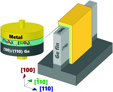
Despite continued innovations prolonging the longevity of the Si microelectronics industry, forward-looking research has regularly examined high carrier mobility, lower bandgap (Eg) materials as alternative channel materials in future complimentary metal–oxide–semiconductor (CMOS) devices and integrated circuits (ICs). Germanium (Ge), in particular, is an attractive candidate due to its high electron and hole mobilities (2× and 4× those of Si, respectively), and its tunable bandgap (either by alloying, strain incorporation, or both). Recently, high-performance CMOS inverters were demonstrated utilizing Ge p-channel (PMOS) and Si n-channel (NMOS) fin field-effect transistors (FinFETs), wherein the Ge layer/channel material was transferred onto a 300 mm Si wafer.1 Although record-setting Ge PMOS performance was achieved in tandem with the lowest equivalent oxide thickness (EOT) to date, 5.7 Å, little was revealed regarding the high-κ gate dielectric utilized. Moreover, the successful integration of Ge PMOS with InxGa1−xAs NMOS (due to its high electron mobility), as opposed to Si NMOS, would revolutionize the ultra-low voltage landscape within the microelectronics industry. In such a configuration, several critical components are important to understand, including: (i) identification of a high-κ dielectric suitable for integration on crystallographically-oriented Ge, thus mimicking the surface orientation present in FinFET devices; (ii) the potential for atomic interdiffusion at the high-κ/Ge heterointerface (e.g., out-diffusion of Ge into HfO2) or the underlying Ge/substrate interface (e.g., Ge-on-insulator, Ge/III–V, or Ge/Si); (iii) the energy band alignment between the high-κ dielectric and Ge (i.e., the valence and conduction band offsets, ΔEV and ΔEC, respectively), needed for understanding of channel carrier confinement; and (iv) thermal stability of the oxide/Ge interface, which would dictate process thermal budgets during dielectric deposition, annealing, and subsequent contact metallization stages. These coupled effects must be investigated in order to fully-utilize Ge-based technologies going forward.2,3 Whereas much recent work4–30 has focused on the HfO2/Al2O3 composite/bi-layer high-κ dielectric combined with an interfacial passivation layer (IPL), typically based on GeO2, it remains difficult to achieve sub-nm EOT. Thus, new passivation schemes have been proposed to realize highly uniform, compositionally abrupt, temperature-stable, and highly-scaled high-κ dielectric/Ge MOS interfaces.1 In so doing, device designers have sought to mitigate direct-tunneling gate leakage current, which is exponential in nature, while maintaining superior gate-channel electrostatic coupling.31 Moreover, the process compatibility of future low-power technologies7–13,16–18,32,33 with existing Si CMOS infrastructure remains a key industry objective.
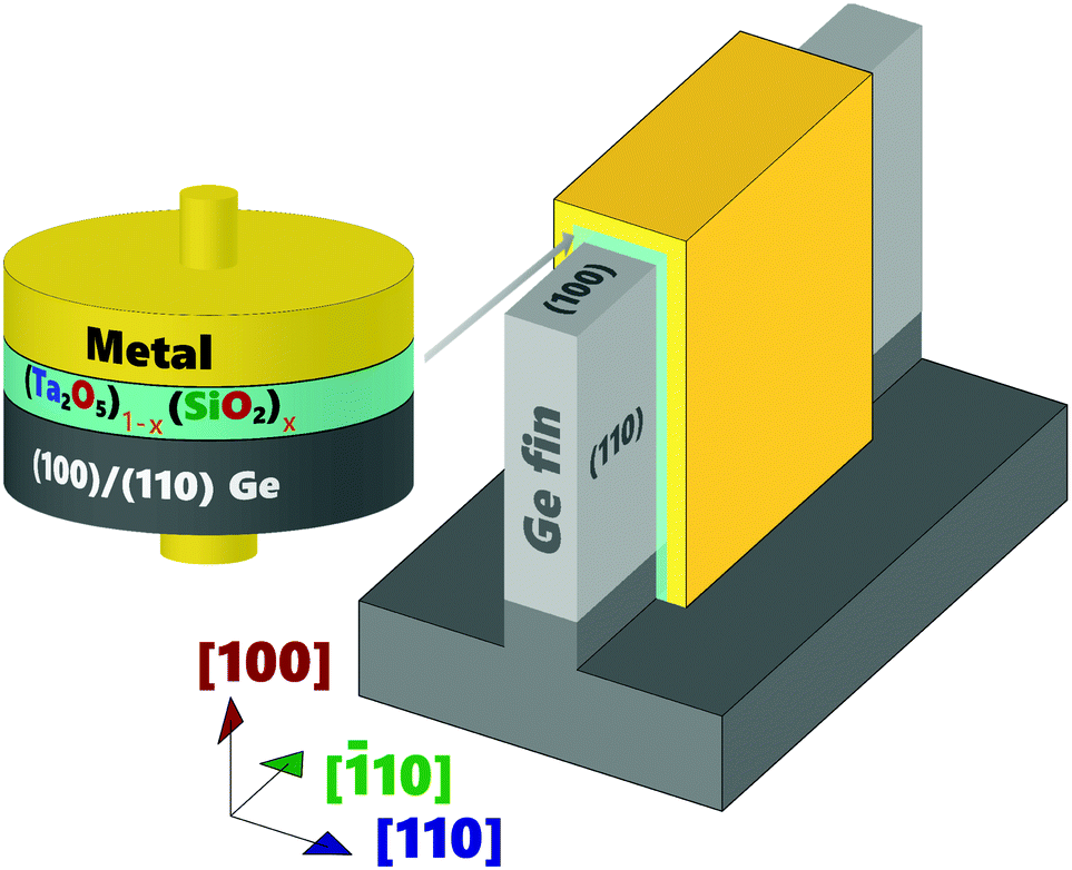
In order to address the above challenges, extensive dielectric research has been performed over the last two decades, with little success in finding simple (non-composite, or non-binary) dielectric systems that mimic the electrical and thermodynamic stability of the SiO2/Si interface.4–38 One promising dielectric, tantalum oxide (Ta2O5), and its silicate (TaSiOx or (Ta2O5)1−x(SiO2)x), has recently found renewed interest as a potential high-κ dielectric for the Ge39–49 and III–V50–53 material systems. TaSiOx was shown to achieve excellent device performance when integrated within a composite TaSiOx/InP gate stack (on InxGa1−xAs-channel FETs), exhibiting low interfacial defect density (Dit), low gate leakage current density (Jg), and high drive current (ION).51 Thus, this study utilizes tantalum(V) ethoxide (Ta2(OC2H5)10) and tris(tert-butoxy)silanol (Si(OH)(OC(CH3)3)3) precursors (for Ta and Si, respectively) to investigate the atomic layer deposition process of (Ta2O5)1−x(SiO2)x onto crystallographically-oriented, epitaxial (001)Ge, (110)Ge, and (111)Ge. These precursors have been previously investigated for the deposition of metal silicates/oxides for high-κ gate dielectrics45,46 and SiO2-based IPLs between HfSiOx dielectrics and their underlying Si substrates.46 Alkylamide precursors can be operated at relatively low temperatures during dielectric ALD, and are an alternative to common amide precursors, such as tetrakis methyl-ethyl amino hafnium (TEMAH) or trimethyl aluminum (TMA) in the cases of HfO2 and Al2O3, respectively, which have been used in the past to deposit dielectrics exhibiting excellent performance. However, utilization of the common amide precursors has often been found to result in deleterious carbon incorporation into the as-deposited dielectric, which can adversely affect the electrical performance and reliability of the dielectric. In this work, crystallographically-oriented Ge thin-films were grown on GaAs substrates by an in-house, solid-source molecular beam epitaxy (MBE) deposition system.54–58 Cross-sectional transmission electron microscopy (X-TEM) analysis was used to determine the thickness of the as-deposited dielectric. X-Ray photoelectron spectroscopy (XPS) analysis was performed in order to study the valence and conduction band discontinues, ΔEV and ΔEC, respectively at the (Ta2O5)1−x(SiO2)x/Ge heterointerface, as well as the chemical bonding environment at the interface. The development of a Ge-based FinFET device architecture, as exemplified in Fig. 1, requires specific understanding of the high-κ gate dielectric/semiconductor interface, including both the chemical and electrical characteristics of the combined material system. As such, the goal of this work is to demonstrate the feasibility of integrating tantalum silicates (TaSiOx) onto Ge by (empirically) elucidating the chemical nature/bonding environment of the TaSiOx/Ge interface, as well as its electronic and physical structure.
 |
| | Fig. 1 Schematic representation of a Ge FinFET utilizing (001)Ge and (110)Ge surface orientations. | |
Experimental
Crystallographically-oriented, epitaxial (001)Ge, (110)Ge, and (111)Ge thin-films were grown on epi-ready AXT Inc.-manufactured (001)GaAs, (110)GaAs, and (111)A GaAs substrates using a vacuum-interconnected, solid-source MBE system with isolated III–V and Ge growth reactors. GaAs native oxide desorption was performed using an arsenic (As) overpressure of ∼105 Torr (inside the III–V growth chamber) utilizing a temperature range of 550 °C to 680 °C, depending on the surface orientation of the initial GaAs substrate. We note that the (001)GaAs substrate required the highest native oxide desorption temperature (680 °C).54,55 Moreover, the temperature referred to in this work is the thermocouple temperature. Additionally, in situ reflection high-energy electron diffraction (RHEED) was used to monitor the wafer surface during oxide desorption and throughout the epitaxy process. Following oxide desorption, a 200 nm-thick GaAs homoepitaxial buffer was grown on each GaAs substrate to create a smooth surface (i.e., to reduce oxide desorption-induced surface roughening). The GaAs homoepitaxial buffers were grown at 500 °C, 550 °C, and 650 °C for the (111)A GaAs, (110)GaAs, and (001)GaAs substrates, respectively. A nominal GaAs growth rate of ∼1 μm h−1 was used throughout this work. After growth of the GaAs homoepitaxial buffer, each sample was cooled below 200 °C under a reducing As overpressure, and finally transferred to the Ge growth chamber for Ge epitaxy. The growth rate and growth temperature used during Ge epitaxy was ∼0.025 μm h−1 and 400 °C, respectively. Several Ge epilayer thicknesses were investigated (grown), after which the terminal Ge/GaAs heterostructure was slowly cooled to ∼50 °C to mitigate thermal stresses in the heterostructure due to thermal expansion coefficient mismatch between the epilayers. Further details regarding the growth process have been reported elsewhere.54,55 Moreover, as previously reported,56–58 the unintentional dopant (uid) concentration of these Ge epilayers fell in the range of 3 × 1018 cm−3 to 5 × 1018 cm−3 and exhibited electron-like conduction (n-type).
Additionally, a Cambridge NanoTech ALD reactor was utilized for the deposition of TaSiOx on each crystallographically-oriented Ge/GaAs heterostructure, using the previously discussed Ta (tantalum(v) ethoxide, Ta(OEt)5) and Si (tris(tert-butoxy)silanol, tBOS) precursors and a growth temperature of 250 °C. The steady-state ALD reactor background pressure prior-to and during deposition was ∼150 mTorr. Each sample surface was treated with a standard solvent clean using acetone, isopropanol, and de-ionized water (DI H2O), followed by a 60 s native oxide removal in a 10:1 buffered oxide etchant (HF) solution, prior to loading into the ALD reactor. Differing thicknesses of TaSiOx (nominally 1.5 nm and 5 nm, see Section B for further details) were deposited using a Si precursor pre-pulsing stage followed by a Ta:Si super-cycle process, noting that DI water provided the oxygen source and N2 (g) provided the purge gas. An initial tBOS/DI H2O cycle was used to prime the sample surface (i.e., pre-pulsing), followed by the 16 (3) Ta:Si super-cycles required for the 5 nm (1.5 nm) nominal TaSiOx thickness. Each super-cycle consisted of one SiO2 cycle per six Ta2O5 cycles, i.e., 6:1 Ta:Si. Pulse times for the Ta and Si precursors were 0.020 s and 0.020 s, respectively, whereas the purge length was 5 s in between each pulse. Similarly, each DI H2O pulse was 0.2 s. The approximate deposition rate following the conditions used herein was ∼0.5 Å per cycle.
Following deposition of the TaSiOx dielectrics, detailed XPS studies were performed in order to reveal the interfacial chemistry, oxide stoichiometry, and heterointerfacial energy band alignments of the crystallographically-oriented TaSiOx/Ge heterostructures. A Phi Quantera Scanning XPS Microprobe equipped with a monochromatic Al-Kα (beam energy of 1486.7 eV) X-ray source was used in the XPS investigations, wherein the (photoelectron) exit angle used was 45°. A low-energy electron flood gun was used throughout spectral acquisition in order to neutralize positive charge accumulation on the oxide surface due to photoelectron generation (electron loss) during measurement. The C 1s core level (CL) binding energy (BE), nominally located at 285.0 eV, was used to correct the measured binding energies for each sample surface. Additionally, the O 1s spectra were recorded in order to determine the TaSiOx bandgap (via the photoelectron energy loss technique, see Section B for further details) for each crystallographic orientation. Curve fitting was performed using CasaXPS v2.3.14, employing a Lorentzian convolution with a Shirley-type background for spectral fitting. Statistical deviation in the Au 4f7/2 CL BE of a Au standard was utilized in the derivation of a ±0.04 eV experimental uncertainty for this work, from which successive uncertainty was estimated using a root-sum-square approach. Lastly, cross-sectional transmission electron microscopy (X-TEM) was performed for the TaSiOx/(001)Ge and TaSiOx/(110)Ge heterostructures in order to elucidate the interfacial properties and more-accurately determine the dielectric (and interfacial layer, if any) thickness(es). The TEM samples were prepared using conventional sample preparation methods, including mechanical polishing, dimpling, and low-temperature Ar+ ion milling.
Results and discussion
A. Oxide and interface chemistry: (Ta2O5)1−x(SiO2)xvia Ta![[thin space (1/6-em)]](https://www.rsc.org/images/entities/h3_char_2009.gif) :Si super-cycling during ALD
:Si super-cycling during ALD
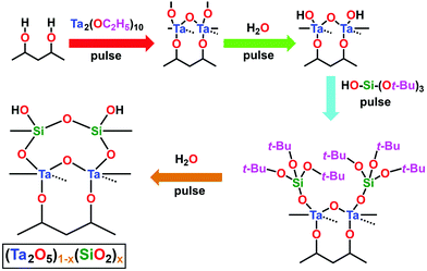
The composite (Ta2O5)1−x(SiO2)x dielectric ALD process investigated herein was performed using n![[thin space (1/6-em)]](https://www.rsc.org/images/entities/i_char_2009.gif) :m super-cycles, where “n” and “m” denote the number of Ta2O5/DI H2O and SiO2/DI H2O cycles, respectively. Fig. 2 outlines the schematic process flow for each step involved in the deposition process of the (Ta2O5)1−x(SiO2)x composite dielectric. Each Ta2O5/DI H2O cycle consisted of one Ta(OEt)5 pulse, followed by one DI H2O pulse, with a short-duration N2 purge separating each precursor pulse. Additionally, one cycle of tBOS pre-pulsing was used prior to the Ta:Si super-cycle process in order to study the efficacy of SiOx interlayer formation on each Ge surface. Fig. 3a presents the first 100 s of a typical TaSiOx ALD process, consisting of (i) the germinal tBOS/DI H2O cycle used to saturate the Ge surface in an initiating Si/SiOx layer, and (ii), a representative 6:1 Ta:Si super-cycle. This deposition process promoted the formation of an in situ interfacial SiOx layer at the TaSiOx/Ge interface.50 Moreover, unlike the more thermodynamically stable and chemically robust native Si oxides, non-stoichiometric, easily-reduced native Ge oxides (i.e., GeOx) have been known to correlate to a high density of (potentially charged) interface states. Furthermore, the water solubility of native Ge oxides, in addition to their low κ value(s), frustrate the ability to effectively scale the equivalent oxide thickness (EOT) of composite dielectrics utilizing GeOx (either native or intentionally re-grown) as an interfacial passivating layer (IPL). As such, the Si (or SiOx) interlayer passivation technique has been suggested as a method to effectively passivate dangling Ge bonds (and therefore, available surface states), as well prevent subsequent oxidation of the Ge surface during dielectric deposition, and was studied herein.29,60–63
:m super-cycles, where “n” and “m” denote the number of Ta2O5/DI H2O and SiO2/DI H2O cycles, respectively. Fig. 2 outlines the schematic process flow for each step involved in the deposition process of the (Ta2O5)1−x(SiO2)x composite dielectric. Each Ta2O5/DI H2O cycle consisted of one Ta(OEt)5 pulse, followed by one DI H2O pulse, with a short-duration N2 purge separating each precursor pulse. Additionally, one cycle of tBOS pre-pulsing was used prior to the Ta:Si super-cycle process in order to study the efficacy of SiOx interlayer formation on each Ge surface. Fig. 3a presents the first 100 s of a typical TaSiOx ALD process, consisting of (i) the germinal tBOS/DI H2O cycle used to saturate the Ge surface in an initiating Si/SiOx layer, and (ii), a representative 6:1 Ta:Si super-cycle. This deposition process promoted the formation of an in situ interfacial SiOx layer at the TaSiOx/Ge interface.50 Moreover, unlike the more thermodynamically stable and chemically robust native Si oxides, non-stoichiometric, easily-reduced native Ge oxides (i.e., GeOx) have been known to correlate to a high density of (potentially charged) interface states. Furthermore, the water solubility of native Ge oxides, in addition to their low κ value(s), frustrate the ability to effectively scale the equivalent oxide thickness (EOT) of composite dielectrics utilizing GeOx (either native or intentionally re-grown) as an interfacial passivating layer (IPL). As such, the Si (or SiOx) interlayer passivation technique has been suggested as a method to effectively passivate dangling Ge bonds (and therefore, available surface states), as well prevent subsequent oxidation of the Ge surface during dielectric deposition, and was studied herein.29,60–63
 |
| | Fig. 2 Schematic representation of the process steps involved in the deposition of the composite dielectric, (Ta2O5)1−x(SiO2)x. The depicted process flow begins subsequent to the pulsing of the Ta precursor, and prior to the pulsing of DI H2O, which is the starting step in this diagram. The dashed lines represent the bond towards the back atom. | |
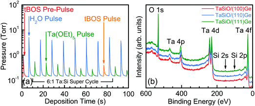 |
| | Fig. 3 (a) Representative TaSiOx ALD process highlighting the initiating tBOS pulse as well as the 6:1 Ta:Si super cycle used in this work. (b) XPS survey spectra recorded from the surface of TaSiOx as-deposited on (100)Ge (red), (110)Ge (blue), and (111)Ge (green) grown on GaAs. The position of the Si 2s and 2p spectral features indicate the incorporation of SiO2 within the composite dielectric, (Ta2O5)1−x(SiO2)x. | |
In order to quantify the SiOx incorporation rate within the composite (Ta2O5)1−x(SiO2)x dielectric, XPS survey spectra were recorded for each crystallographically-oriented TaSiOx/Ge heterostructure's surface, as shown in Fig. 3b. A 30 s, low-energy (E ≤ 1 keV) Ar+ ion sputtering preceded spectral acquisition so as to remove residual surface contamination and minimize spurious extrinsic binding energy (BE) shifts. One can find from Fig. 3b that the Si 2p and Ta 4d5/2 BEs (∼102.3 ± 0.04 eV and ∼229.7 ± 0.04 eV, respectively) correspond to those of the Si4+ and Ta5+ oxidation states (SiO2 and Ta2O5, respectively), suggesting the stoichiometric formation of both constituent oxides during deposition. Moreover, utilizing the integrated photoelectron intensity for the Ta 4f, Si 2p, and O 1s spectral features, the concentration of SiO2 within the as-deposited TaSiOx composite dielectric was found to be 17.5%, in close agreement with the nominal (targeted) 20% SiO2 composition.
A.1. Sputter depth-dependent XPS analysis of TaSiOx dielectrics on epitaxial Ge.
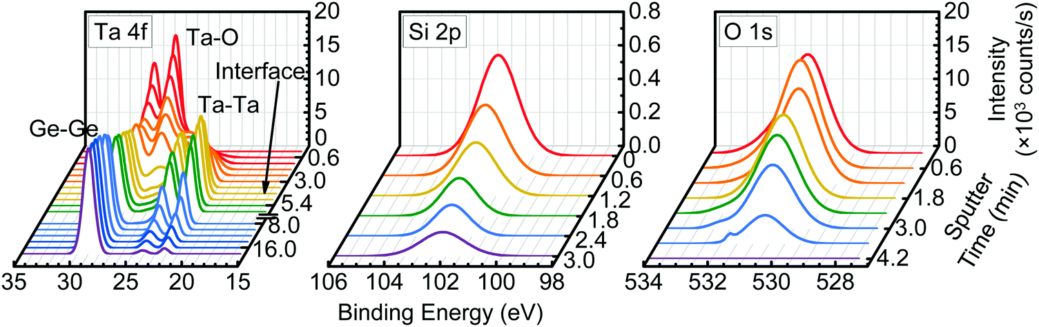
The SiO2 incorporation uniformity was further investigated via XPS sputter depth profiling of the as-deposited TaSiOx/(001)Ge specimen. Fig. 4 presents the Ta 4f and Ge 3d BE spectra as a function of sputter time for a nominally 5 nm TaSiOx dielectric deposited on (001)Ge. Likewise, Fig. 4 show the Si 2p and O 1s BE spectra, respectively, of the same. As shown in Fig. 4, an additional Ta 4f doublet appeared at the onset of sputtering and remain unchanged in BE throughout the entirety of the dielectric. The Ta 4f7/2 and Ta 4f5/2 BEs of the secondary doublet, 22.2 ± 0.04 eV and 24.05 ± 0.04 eV, respectively, corresponded to the metallic Ta bond (i.e., Ta–Me). The consistency in BE position of the secondary doublet suggests that it was not a measurement artifact induced by preferential sputtering within the Ta2O5 constituent oxide.59–72 This conclusion was supported by previous work demonstrating negligible change in Ta2O5 stoichiometry due to Ar+ depth profiling; i.e., within experimental error, the Ta2O5 was not reduced via low-energy (E = 1.5 keV) Ar+ ion bombardment.70,73 Besides, any such preferential sputtering would concomitantly and quantifiably alter the measured O 1s BE (∼530.8 ± 0.04 eV), which was not observed in this work. Likewise, no quantifiable BE shift of the Si 2p spectra was observed as a function of sustained Ar+ sputtering, indicating that the Si–O bond (and not the Si–Me bond) remained the dominant Si bonding environment within TaSiOx.
 |
| | Fig. 4 XPS sputter depth profile of the as-deposited TaSiOx/(100)Ge structure, consisting of the Ta 4f and Ge 3d (left), Si 2p (middle), and O 1s binding energy regions (right). | |
As such, the metallic Ta bond observed in Fig. 4 has two likely origins: (i) a persistent Ta–Ta bond that is relatively uniform throughout TaSiOx; or (ii), an interaction between Ge and Ta atoms at the TaSiOx/Ge interface, followed by the subsequent up-diffusion of the Ta–Ge bond. Although formation of Ta–Ta bonds cannot be ruled out during the deposition of TaSiOx, their presence would imply (i) an incomplete Ta(OEt)5–DI H2O reaction, and/or (ii) the thermal decomposition of the Ta(OEt)5 precursor. However, in both scenarios, spectral features corresponding to residual hydrocarbons and Ta suboxides (e.g., Ta2O3−) would be expected in the recorded XPS spectra. Notably, neither of these distinct signifiers were observed herein. Consequently, we attribute the secondary Ta 4f doublet to the formation and diffusion of Ta–Ge bonds during the ALD of TaSiOx.
Evidence for this conclusion can be found in Fig. 4, wherein the secondary Ta 4f doublet persisted in the metallic BE state beyond the point at which TaSiOx had been wholly removed (sputtered) from the Ge surface. This point in time, 3.6 min < t ≤ 4.2 min, corresponded to the absence of the O 1s singlet in the measured XPS spectra, as shown in Fig. 4. The observation of the Ta 4f doublet in its metallic BE state for t > 4.2 min indicated the diffusion of Ta within Ge, and the increased likelihood for Ta–Ge bond formation. In the event that a single tBOS sub-cycle was insufficient to wholly encapsulate the Ge surface, the remaining OH-terminated Ge would have been partially exposed to an oxidation source in the form of DI H2O (g). What is more, examining the standard Gibbs free energies of formation for Ta2O5 and GeO2 reported in the literature, −1911 kJ mol−1 and −521 kJ mol−1 at 293 K, respectively,74 one might expect preferential bonding of O with Ta at the TaSiOx/Ge interface. We therefore posit that TaGe2 formation at the non-Si(Ox)-encapsulated TaSiOx/Ge interface, and subsequent up/down-diffusion enhanced by the formation of Ge–O, occurs during the ALD of TaSiOx under the deposition conditions utilized herein.
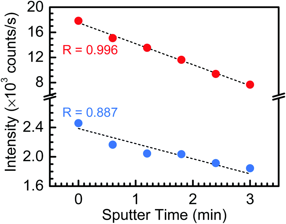
Lastly, Fig. 5 presents the fitted Ta 4f5/2 and Si 2p peak intensities as a function of sputtering time, up to 3 min (i.e., up to the loss of the Si 2p spectral feature). One can find from Fig. 5 that the fitted peak intensities of both the Ta 4f5/2 and Si 2p peaks decreasing monotonically with increased sputtering time, indicating: (i) a lack of preferential sputtering between the constituent Ta2O5 and SiO2 oxides; and (ii) a uniform SiO2 incorporation throughout the TaSiOx composite dielectric.
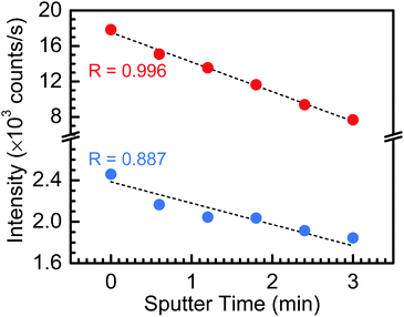 |
| | Fig. 5 Ta 4f and Si 2p core level binding energy peak intensities as a function of sputtering time, wherein the peak intensity of each constituent element (corresponding to the Ta2O5 and SiO2 component oxides) decreases proportionally with increasing sputtering time. | |
A.2. TaSiOx/Ge heterointerfacial characterization via TEM.
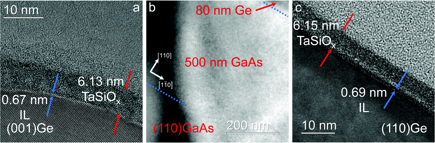
Fig. 6 shows the cross-sectional TEM micrographs of (a) TaSiOx on (001)Ge/GaAs, (b) the epitaxial Ge/(110)GaAs heterointerface, and (c) TaSiOx on (110)Ge/GaAs, respectively. The abrupt Ge-on-GaAs heterointerface, as observed in Fig. 6b, confirmed the high-quality Ge epitaxy. Furthermore, one can find from Fig. 6a and c that the TaSiOx dielectric thickness was approximately 6.1 nm–6.2 nm, with an additional ∼0.7 nm interfacial layer formed at the oxide/semiconductor interface due to the intentional tBOS/DI H2O cycle provided prior to composite TaSiOx deposition.50 This is in good agreement with previous results investigating the integration of metal silicates on (001)InxGa1−xAs and (110)InxGa1−xAs thin-films, wherein an 8 Å (0.8 nm) SiOx interfacial layer was observed at the oxide/semiconductor interface.46 This suggests that no catalytic reaction between the Ta and Si precursors (Ta(OEt)5 and tBOS, respectively) occurred for the deposition conditions used herein. Moreover, as evidenced by the sputter depth-dependent XPS analysis discussed earlier, it cannot be ruled out that the interfacial oxide also contains constituent GeOx and TaOx suboxides. If so, whereas a primarily SiOx-based interlayer would increase the thermodynamic stability of the oxide/semiconductor heterointerface, one might expect that Ge- and Ta-suboxide incorporation would reduce interlayer robustness, even if it might (temporarily) passivate Ge dangling bonds at the Ge surface.29,30
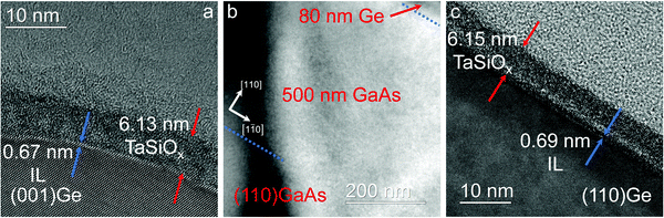 |
| | Fig. 6 Cross-sectional transmission electron micrographs showing the (a) TaSiOx/(001)Ge heterointerface, (b) Ge epilayer as-grown on (110)GaAs using a 500 nm GaAs homoepitaxial buffer, and (c), the TaSiOx/(110)Ge heterointerface. The interfacial SiOx-based passivation layer is highlighted in each high-resolution micrograph. | |
B. Energy band alignment properties of the TaSiOx/Ge heterointerface
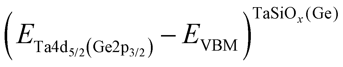
To evaluate the valence band discontinuity (ΔEV) at the TaSiOx dielectric/semiconductor interface, XPS spectra were recorded from: (i) nominally 5 nm (Ta2O5)1−x(SiO2)x on crystallographically-oriented (001)Ge, (110)Ge, and (111)Ge, i.e., “bulk-like” TaSiOx; (ii) nominally 1.5 nm (Ta2O5)1−x(SiO2)x on crystallographically-oriented (001)Ge, (110)Ge, and (111)Ge, i.e., the oxide/semiconductor interface; and (iii), the surface of the as-grown (001)Ge, (110)Ge, and (111)Ge thin-films integrated on GaAs, i.e., “bulk-like” Ge. Eqn (1), following the methodology developed by Kraut et al.75 as utilized in previous studies,50,54,56,59,76–80 was used to determine the ΔEV:| |  | (1) |
where 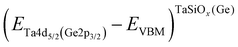 is the BE separation between the Ta (Ge) 4d5/2 (2p3/2) state and the VBM of the respective material and is the BE separation between the Ta 4d5/2 and Ge 2p3/2 states measured at the interface. Similarly, the conduction band offset (ΔEC) can be determined using the following relation:
| | 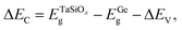 | (2) |
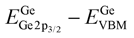
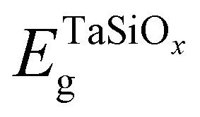
where  and EGeg are the bandgaps of TaSiOx and Ge, respectively, and ΔEV is the measured valence band offset. Additionally, the bandgap (Eg) of the as-deposited TaSiOx dielectrics was determined for each crystallographic orientation utilizing the O 1s photoelectron energy loss spectra. Explicitly, the binding energy separation between the “onset” of photoelectron emission (with respect to the spectral background immediately following the O 1s peak) and the center of the fitted O 1s spectral feature(s) provides a direct method in determining an oxide's bandgap. This is due to the nature of dielectric films, which require less energy for band-to-band excitation (i.e., the lowest/principal valence and conduction bands) as opposed to plasmon losses.70 A moderate range of bandgap values, between 4.4 eV–4.65 eV, have been reported in the literature, with variability in the measured bandgap stemming from the deposition method(s) utilized, or empirical method in determining the oxide bandgap (including XPS, photoluminescence and photoemission spectroscopies) of Ta2O5.34–44 Cevro et al.39 reported an optical bandgap varying from 4.3 eV–9.0 eV for x = 1.0 to x = 0.0 atomic mole fraction of Ta2O5 in the composite (Ta2O5)1−x(SiO2)x dielectric. However, Adelmann et al.40 found that for ALD TaSiOx on Si, the bandgap starts to vary from ∼4.5 eV for x = 0.0 up to ∼4.9 eV for x = 0.5.40 As such, a precise determination of the TaSiOxEg is important in order to accurately determine ΔEC at the TaSiOx/Ge heterointerface. Lastly, as discussed in the Experiments section, we note that statistical deviation in the Au 4f7/2 CL BE of a Au standard was utilized in the derivation of a ±0.04 eV experimental uncertainty for this work, from which successive uncertainty was estimated using a root-sum-square approach.78–80
B.1. Energy band alignment at the TaSiOx/(001)Ge heterointerface.
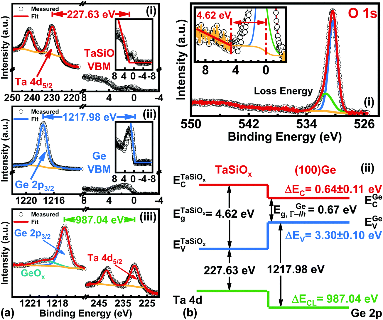
Fig. 7a shows the: (i) Ta 4d core-level (CL) BE and valence band (VB) spectra recorded from the bulk-like TaSiOx surface on (001)Ge; (ii) Ge 2p CL BE and VB spectra recorded from the bulk-like (001)Ge surface; and (iii), Ta 4d and Ge 2p CL BE spectra recorded at the TaSiOx/(001)Ge interface. We note that the insets to Fig. 7a(i) and b(i) show the fitting of each material's VB spectra in order to determine their associated valence band maxima (VBM). Each VBM was determined by linearly fitting the onset of photoemission from the VB density of states with respect to the background photoemission. Similarly, Fig. 7b(i) shows the O 1s CL BE spectra recorded for the TaSiOx/(001)Ge surface, from which a TaSiOxEg = 4.62 ± 0.06 eV was determined following the procedures outlined earlier. Likewise, the measured BE separations between the samples shown in Fig. 7a were found to be: (i) 227.63 ± 0.06 eV; (ii) 1217.98 ± 0.06 eV; and (iii), 987.04 ± 0.06 eV. Substituting these BE separations into eqn (1), the empirical ΔEV at the TaSiOx/(001)Ge interface was determined, resulting in ΔEV = 3.30 ± 0.1 eV, as shown in Fig. 7b(ii). Utilizing eqn (2), along with the measured TaSiOxEg and the literature-reported Ge bandgap (EGeg = 0.67 eV, as measured between the L-valley conduction band minimum and the valence band maximum at the Γ point), ΔEC was calculated to be 0.64 ± 0.11 eV. Table 1 summarizes the experimental energy band alignment parameters determined herein.
 |
| | Fig. 7 XPS spectra of the: (a)(i) Ta 4d5/2 CL and VBM of “bulk-like” TaSiOx deposited on (001)Ge/GaAs; (a)(ii) Ge 2p3/2 CL and VBM of “bulk-like” (001)Ge/GaAs; (a)(iii) Ta 4d5/2 and Ge 2p3/2 CLs recorded at the TaSiOx/(001)Ge heterointerface; (b)(i) O 1s loss spectra used to extract the TaSiOx bandgap (4.62 ± 0.06 eV); and (b.ii), the resulting band alignment at the TaSiOx/(001)Ge oxide/semiconductor heterointerface. | |
Table 1 XPS-determined binding energy separations and corresponding energy band offset parameters for ALD amorphous TaSiOx on epitaxial (001)Ge/GaAs, (110)Ge/GaAs, and (111)Ge/GaAs thin-films
| Binding energy separation |
(001)Ge |
(110)Ge |
(111)Ge |

|
1217.98 ± 0.06 |
1217.94 ± 0.06 |
1217.92 ± 0.06 |

|
227.63 ± 0.06 |
227.51 ± 0.06 |
227.54 ± 0.06 |

|
−987.04 ± 0.06 |
−987.07 ± 0.06 |
−987.13± 0.06 |
| ΔEV (eV) |
−3.30 ± 0.10 |
−3.36 ± 0.10 |
−3.25 ± 0.10 |
|
E
g of TaSiOx (eV) |
4.62 ± 0.06 |
4.66 ± 0.06 |
4.65 ± 0.06 |
| ΔEC (eV) |
0.65 ± 0.11 |
0.63 ± 0.11 |
0.73 ± 0.11 |
B.2. Energy band alignment at the TaSiOx/(110)Ge heterointerface.
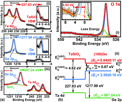
As demonstrated in Fig. 1, future Ge FinFET devices would utilize both (001)Ge and (110)Ge crystallographic orientations, with each surface orientation functioning as one (of three) MOS interfaces. As such, characterization of the crystallographic orientation-dependence of the TaSiOx/Ge energy band alignment would provide vital guidance for device engineers seeking to utilize both material systems in future FET architectures. Correspondingly, and following the approach outlined in the preceding sections, ΔEV and ΔEC were determined at the TaSiOx/(110)Ge heterointerface, employing eqn (1) and (2). Fig. 8a shows the: (i) Ta 4d CL BE and VB spectra recorded from the bulk-like TaSiOx surface on (110)Ge; (ii) Ge 2p CL BE and VB spectra recorded from the bulk-like (110)Ge surface; and (iii), Ta 4d and Ge 2p CL BE spectra recorded at the TaSiOx/(110)Ge interface. Likewise, Fig. 8b(i) shows the O 1s CL BE spectra recorded for the TaSiOx/(110)Ge surface, from which a TaSiOxEg = 4.66 ± 0.06 eV was determined. Using the measured BE separations highlighted in Fig. 8a, and the empirically-determined TaSiOx bandgap on the (110)Ge surface given above, ΔEV and ΔEC were found to be 3.36 ± 0.1 eV and 0.63 ± 0.11 eV, respectively, again using EGeg = 0.67 eV, as shown in Fig. 8b(ii). As before, Table 1 provides all binding energy parameters used in the determination of the energy band offsets at the TaSiOx/(110)Ge interface.
 |
| | Fig. 8 XPS spectra of the: (a)(i) Ta 4d5/2 CL and VBM of “bulk-like” TaSiOx deposited on (110)Ge/GaAs; (a)(ii) Ge 2p3/2 CL and VBM of “bulk-like” (110)Ge/GaAs; (a)(iii) Ta 4d5/2 and Ge 2p3/2 CLs recorded at the TaSiOx/(110)Ge heterointerface; (b)(i) O 1s loss spectra used to extract the TaSiOx bandgap (4.66 ± 0.06 eV); and (b)(ii), the resulting band alignment at the TaSiOx/(110)Ge oxide/semiconductor heterointerface. | |
B.3. Energy band alignment at the TaSiOx/(111)Ge heterointerface.
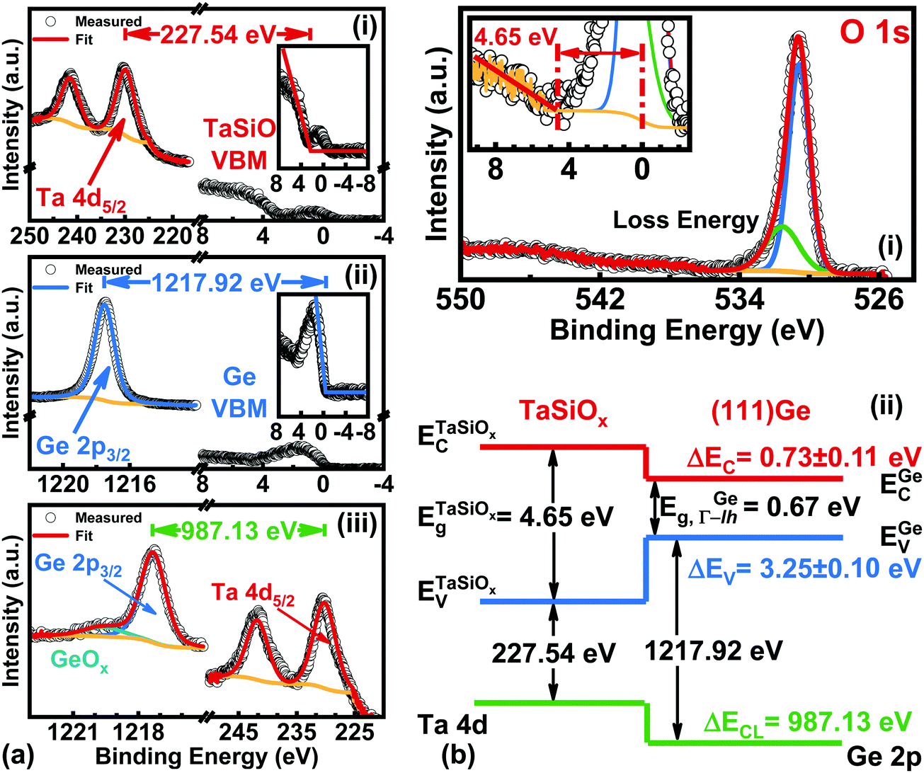
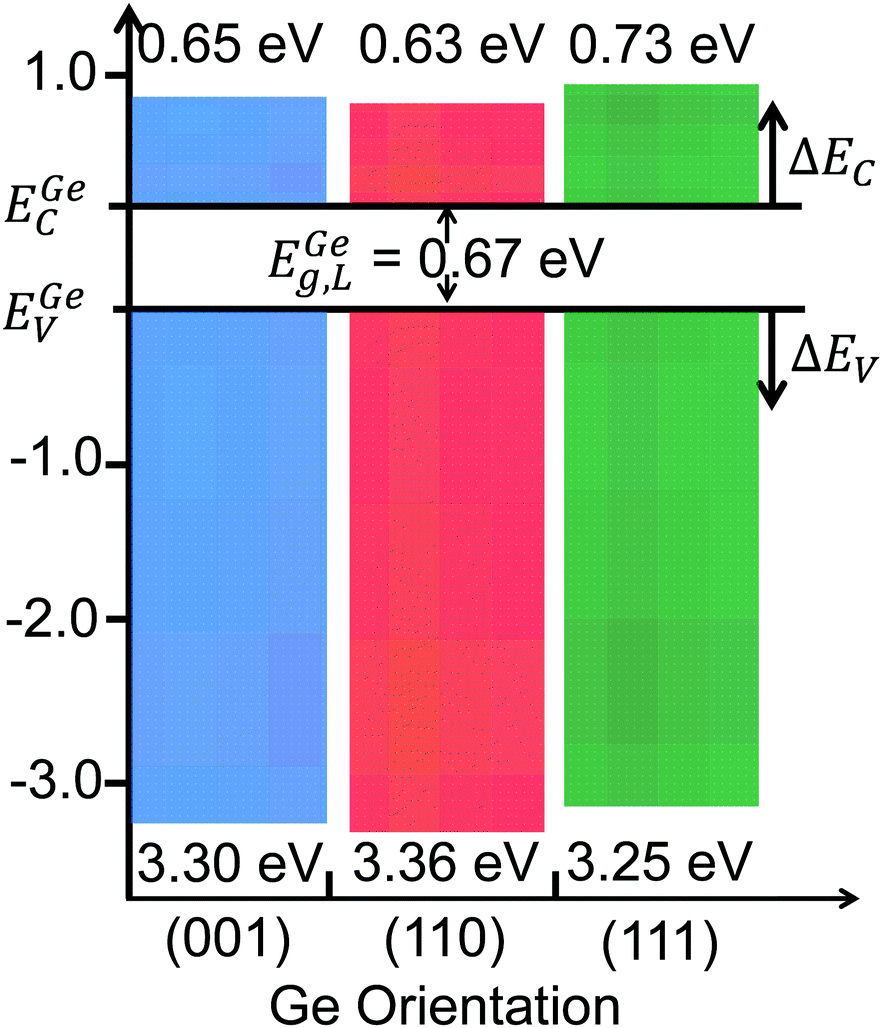
Fig. 9a shows the: (i) Ta 4d CL BE and VB spectra recorded from the bulk-like TaSiOx surface on (111)Ge; (ii) Ge 2p CL BE and VB spectra recorded from the bulk-like (111)Ge surface; and (iii), Ta 4d and Ge 2p CL BE spectra recorded at the TaSiOx/(111)Ge interface. Similarly, Fig. 9b(i) shows the O 1s CL BE spectra recorded for the TaSiOx/(111)Ge surface, with a correspond TaSiOxEg = 4.65 ± 0.06 eV. Combining the binding energy separation data presented in Fig. 9a, with the measured TaSiOx/(111)Ge dielectric Eg, the empirical ΔEV and ΔEC at the TaSiOx/(111)Ge interface were found to be 3.25 ± 0.1 eV and 0.73 ± 0.11 eV, respectively. These results, and their binding energy separation dependencies, are also presented in Table 1. Lastly, Fig. 10 summarizes the energy band alignment parameters for TaSiOx on each crystallographic orientation for the Ge epilayers studied in this work. One can find from Fig. 10 (and Table 1) that ΔEV was almost independent of the Ge surface orientation. Moreover, the relatively large ΔEV values observed (as compared to ΔEC) suggest improved hole confinement, broadly speaking, whereas the observed ΔEC > 0.6 ± 0.11 eV would likely remain suitable for electron confinement under low voltage (VDD ≤ 0.5 V) operating conditions.
 |
| | Fig. 9 XPS spectra of the: (a)(i) Ta 4d5/2 CL and VBM of “bulk-like” TaSiOx deposited on (111)Ge/GaAs; (a)(ii) Ge 2p3/2 CL and VBM of “bulk-like” (111)Ge/GaAs; (a.iii) Ta 4d5/2 and Ge 2p3/2 CLs recorded at the TaSiOx/(111)Ge heterointerface; (b)(i) O 1s loss spectra used to extract the TaSiOx bandgap (4.65 ± 0.06 eV); and (b)(ii), the resulting band alignment at the TaSiOx/(111)Ge oxide/semiconductor heterointerface. | |
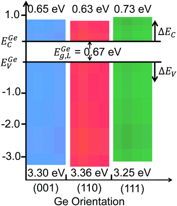 |
| | Fig. 10 Band offset distributions for TaSiOx on the (001)Ge, (110)Ge, and (111)Ge surface orientations. | |
C. Surface chemistry at TaSiOx/(001)Ge, (110)Ge, and (111)Ge heterointerfaces
The surface chemistry at the TaSiOx composite dielectric/Ge heterointerface is important, as it is intrinsically linked to the electrical behavior of fabricated MOS devices.58 One can find from Fig. 7a(iii), 8a(iii) and 9a(iii) that the sharp binding energy peak located at ∼1217.3 ± 0.04 eV, having a full-width at half-maximum (FWHM) of 1.25 eV–1.30 eV (± 0.04 eV), is characteristic of the Ge0 oxidation state, or simply put, the Ge–Ge bond attributable to the epitaxial Ge layer(s). On the other hand, the shoulder located at higher binding energy (ΔBE ∼ 2.2 ± 0.06 eV), is indicative of the formation of an interfacial GeOx transition region. It should be noted that such a GeOx transition region was observed across all orientations. The conclusion that a GeOx–containing transition region exists at the TaSiOx/Ge interface is highlighted by the absence of a corresponding shoulder in the “bulk-like” Ge XPS spectra recorded from the Ge epilayer surface, as shown in Fig. 7a(ii), 8a(ii) and 9a(ii). One can find from Fig. 7a(ii), 8a(ii) and 9a(ii) that the “bulk-like” Ge XPS spectra (for each crystallographic orientation) were de-convolved into isolated Gaussian peaks corresponding to the Ge0 oxidation state (i.e., the Ge–Ge metal bond) absent of any shoulder, indicating a lack of GeOx on the surface of the as-grown Ge epilayer. It has already been shown that the ALD of Ta2O5 on Si results in an interfacial SiO2 layer formed even at low deposition temperatures.46 Moreover, given the pre-pulsing of TBOS prior to TaSiOx ALD, and its resulting (intentional) ∼7 Å interfacial layer formation, as demonstrated via TEM analysis, it is further possible that this interfacial transition region consists of a complex, non-stoichiometric mixture of SiOx, GeOx, and TaOx oxides/suboxides. Such a picture is consistent with the Ta and Ge diffusion mechanism posited in Section A.1, wherein exposure of the OH-terminated Ge surface (in regions not saturated by the TBOS precursor) to DI H2O (g) would result in un-intentional oxidation of the Ge surface (as well as possible Ta–Ge bond formation). Such un-intentional GeOx formation could likewise be exacerbated by diffusion of O downward, through the dielectric, and toward the interfacial oxide transition region. It is interesting to note that the width of this transition region, ∼7 Å, mirrors that of similar TaSiOx dielectric depositions performed (via ALD) on (nominally) In0.53Ga0.47As/(001) and (110)InP structures.50
Lastly, Fig. 7b(i), 8b(i) and 9b(i) show the recorded O 1s spectra for each crystallographic orientation of Ge investigated in this work. As is evident from these figures, all O 1s spectral features were de-convolved into two Gaussian components – one peak exhibiting a narrow FWHM, and the other being a broad shoulder located at higher binding energy (relative to the former). The Gaussian peak located at lower binding energies (∼530.5 ± 0.04 eV) is characteristic of the Ta5+ oxidation state in Ta2O5, which indicates the stoichiometric oxidation of Ta. The shoulder peak observed at higher binding energy (∼531.5 ± 0.04 eV) was attributed to Ta–O–Si bonding, which was corroborated viaFig. 4 and 5 demonstrating the (uniform) incorporation of SiO2 into the Ta2O5 matrix. Moreover, such SiO2 incorporation could be expected to result in improved oxide thermal characteristics, such as increased recrystallization temperatures, as was observed in the case of HfSiOx dielectrics. Too, the absence of suboxide formation in the bulk of the TaSiOx dielectric is indicative of high-quality dielectric deposition.
Conclusions
In this work, (Ta2O5)1−x(SiO2)x has been deposited by ALD, using Ta2(O-C2H5)10 and ((CH3)3CO)3Si-OH for the Ta and Si precursors, respectively, on to crystallographically-oriented, epitaxial (001)Ge, (110)Ge, and (111)Ge thin-films grown on (001)GaAs, (110)GaAs, and (111)A GaAs substrates. Intentional pre-pulsing of the Si precursor (prior to composite TaSiOx dielectric deposition) resulted in the formation of a SiOx IPL at the dielectric/Ge interface, with the potential to passivate dangling bonds on the Ge surface, and thereby deleterious interfacial charge. Sputter depth-dependent XPS analysis through the TaSiOx/Ge heterostructure revealed uniform Si incorporation throughout the composite TaSiOx oxide, and a measurable degree of Ge and Ta atomic cross-diffusion across the oxide/semiconductor interface. Cross-sectional TEM analysis identified a distinct SiOx IPL present on the Ge surface, likely originating in a complex, quaternary oxide structure (i.e., that of GeOx, SiOx, and TaOx) formed before and during the deposition of the overlying TaSiOx oxide. Additionally, the bandgap of as-deposited, Ta-rich Ta0.8Si0.2Ox dielectrics was determined via XPS to be in the range of 4.62 eV–4.66 (±0.06 eV), which was in excellent agreement with the bandgap values found in literature. The energy band discontinuities, i.e., ΔEV and ΔEC, were found to be >3.0 ± 0.1 eV and >0.6 ± 0.11 eV, respectively, for all crystallographic orientations, which would suggest increased hole confinement across a wide operating voltage range, and sufficient electron confinement when operated at low drive voltages (i.e., VDD < 0.5 V). Moreover, the relatively high conduction and large valence band offsets observed in the TaSiOx/Ge material system merits further investigation toward the development of Ge-based MOS devices for low- and ultra-low-power applications.
Author contributions
Michael Clavel: investigation, methodology, measurement, analysis, visualization, writing – review and editing; Shuvodip Bhattacharya: analysis, review and editing; Mantu Hudait: resources, supervision, project administration, funding acquisition, methodology, data curation, writing original draft, reviewing and editing.
Conflicts of interest
The authors declare no competing financial interests.
Acknowledgements
The authors gratefully acknowledge Jheng–Sin Liu for TEM instrumentation and measurement. The authors also acknowledge the Nanocharacterization and Fabrication Laboratory – Institute for Critical Technology and Applied Science, as well as the Virginia Tech Nanofabrication facilities, for assistance during materials characterization and synthesis.
References
- W. Rachmady, A. Agrawal, S. H. Sung, G. Dewey, S. Chouksey, B. Chu-Kung, G. Elbaz, P. Fischer, C. Y. Huang, K. Jun, B. Krist, M. Metz, T. Michaelos, B. Mueller, A. A. Oni, R. Paul, A. Phan, P. Sears, T. Talukdar, J. Torres, R. Turkot, L. Wong, H. J. Yoo and J. T. Kavalieros, IEDM Tech. Dig., 2019, 29.7.1–29.7.4 Search PubMed.
- J.-S. Liu, M. B. Clavel and M. K. Hudait, IEEE J. Electron Devices Soc., 2019, 7, 210–218 CAS.
-
S. Datta, M. K. Hudait, M. L. Doczy, J. T. Kavalieros, M. Amlan, J. K. Brask, B.-Y. Jin, M. Metz and R. S. Chau, US Pat. #2007/0138565, 2007.
- H. Wu, W. Wu, M. Si and P. D. Ye, IEDM Tech. Dig., 2015, 2.1.1–2.1.4 Search PubMed.
- H. Wu, W. Luo, H. Zhou, M. Si, J. Zhang and P. D. Ye, Symp. VLSI Technol., Dig., 2015, T58–T59 Search PubMed.
- A. Agrawal, M. Barth, G. B. Rayner Jr., V. T. Arun, C. Eichfeld, G. Lavallee, S.-Y. Yu, X. Sang, S. Brookes, Y. Zheng, Y.-J. Lee, Y.-R. Lin, C.-H. Wu, C.-H. Ko, J. LeBeau, R. Engel-Herbert, S. E. Mohney, Y.-C. Yeo and S. Datta, IEDM Tech. Dig., 2014, 414–417 Search PubMed.
- M. Heyns, A. Alian, G. Brammertz, M. Caymax, Y. C. Chang, L. K. Chu, B. De Jaeger, G. Eneman, F. Gencarelli, G. Groeseneken, G. Hellings, A. Hikavyy, T. Y. Hoffmann, M. Houssa, C. Huyghebaert, D. Leonelli, D. Lin, R. Loo, W. Magnus, C. Merckling, M. Meuris, J. Mitard, L. Nyns, T. Orzali, R. Rooyackers, S. Sioncke, B. Soree, X. Sun, A. Vandooren, A. S. Verhulst, B. Vincent, N. Waldron, G. Wang, W. E. Wang and L. Witters, IEDM Tech. Dig., 2011, 13.1.1–13.1.4 Search PubMed.
-
S. Takagi and M. Takenaka, Paper MP-CK-3 presented in IEEE Nanotechnology Materials and Devices Conference (IEEE NMDC 2013), October 7–9, 2013, National Cheng Kung University, Taiwan, 1–2.
- A. Chin, C. Chen, D. S. Yu, H. L. Kao, S. P. McAlister and C. C. Chi, Mater. Sci. Semicond. Process., 2006, 9, 711–715 CrossRef CAS.
- M. A. Wistey, U. Singisetti, G. J. Burek, E. Kim, B. J. Thibeault, A. Nelson, J. Cagnon, Y.-J. Lee, S. R. Bank, S. Stemmer, P. C. McIntyre, A. C. Gossard and M. J.-W. Rodwell, ECS Trans., 2009, 19, 361–372 CrossRef CAS.
- S. Takagi and M. Takenaka, ECS Trans., 2011, 35, 279–298 CrossRef CAS.
- T. Irisawa, M. Oda, Y. Kamimuta, Y. Moriyama, K. Ikeda, E. Mieda, W. Jevasuwan, T. Maeda, O. Ichikawa, T. Osada, M. Hata and T. Tezuka, Symp. VLSI Technol., Dig., 2013, T56–T57 Search PubMed.
- M. Yokoyama, S. H. Kim, R. Zhang, N. Taoka, Y. Urabe, T. Maeda, H. Takagi, T. Yasuda, H. Yamada, O. Ichikawa, N. Fukuhara, M. Hata, M. Sugiyama, Y. Nakano, M. Takenaka and S. Takagi, Symp. VLSI Technol., Dig., 2011, 60–61 Search PubMed.
- A. Toriumi and T. Nishimura, Jpn. J. Appl. Phys., 2018, 57, 010101-1–010101-44 CrossRef.
- E. D. Kurniawan, K.-H. Peng, S.-Y. Yang, Y.-Y. Yang, V. Thirunavukkarasu, Y.-H. Lin and Y.-C. Wu, Jpn. J. Appl. Phys., 2018, 57, 04FD17-1–04FD17-6 CrossRef.
- D. Lin, G. Brammertz, S. Sioncke, C. Fleischmann, A. Delabie, K. Martens, H. Bender, T. Conard, W. H. Tseng, J. C. Lin, W. E. Wang, K. Temst, A. Vatomme, J. Mitard, M. Caymax, M. Meuris, M. Heyns and T. Hoffmann, IEDM Tech. Dig., 2009, 327–330 Search PubMed.
- S. Takagi, R. Zhang, J. Suh, S.-H. Kim, M. Yokoyama, K. Nishi and M. Takenaka, Jpn. J. Appl. Phys., 2015, 54, 06FA01-1–06FA01-18 Search PubMed.
- V. Deshpande, V. Djara, E. O’Connor, P. Hashemi, T. Morf, K. Balakrishnan, D. Caimi, M. Sousa, J. Fompeyrine and L. Czomomaz, Jpn. J. Appl. Phys., 2017, 56, 04CA05-1–04CA05-7 CrossRef.
- P. Goley and M. K. Hudait, Materials, 2014, 7, 2301–2339 CrossRef CAS PubMed.
- M. Takenaka, R. Zhang and S. Takagi, IEEE Int. Reliab. Phys. Symp. Proc., 2013, 4C.1.1–4C.1.8 Search PubMed.
- R. Zhang, T. Iwasaki, N. Taoka, M. Takenaka and S. Takagi, Symp. VLSI Technol., Dig., 2011, 56–57 CAS.
-
J. W. Anthis and K. Z. Ahmed, Pat. #WO2014/035933 A1, 2014.
- Y. H. Tan, K. S. Yew, K. H. Lee, Y.-J. Chang, K.-N. Chen, D. S. Ang, E. A. Fitzgerald and C. S. Tan, IEEE Trans. Electron Devices, 2013, 60, 56–62 CAS.
- H. Y. Yu, M. Ishibashi, J. H. Park, M. Kobayashi and K. C. Saraswat, IEEE Electron Device Lett., 2009, 30, 675–677 CAS.
- R. Zhang, T. Iwasaki, N. Taoka, M. Takenaka and S. Takagi, Appl. Phys. Lett., 2011, 98, 112902-1–112902-3 Search PubMed.
- D. Kuzum, T. Krishnamohan, A. J. Pethe, A. K. Okyay, Y. Oshima, Y. Sun, J. P. McVittie, P. A. Pianetta, P. C. McIntyre and K. C. Saraswat, IEEE Electron Device Lett., 2008, 29, 328–330 CAS.
- Y. Oshima, M. Shandalov, Y. Sun, P. Pianetta and P. C. McIntyre, Appl. Phys. Lett., 2009, 94, 183102-1–183102-3 Search PubMed.
- M. J.-H. van Dal, G. Vellianitis, G. Doornbos, B. Duriez, T. M. Shen, C. C. Wu, R. Oxland, K. Bhuwalka, M. Holland, T. L. Lee, C. Wann, C. H. Hsieh, B. H. Lee, K. M. Yin, Z. Q. Wu, M. Passlack and C. H. Diaz, IEDM Tech. Dig., 2012, 521–524 CAS.
- R. Pillarisetty, B. Chu-Kung, S. Corcoran, G. Dewey, J. T. Kavalieros, H. Kennel, R. Kotlyar, V. Le, D. Lionberger, M. Metz, N. Mukherjee, J. Nah, W. Rachmady, M. Radosavljevic, U. Shah, S. Taft, H. Then, N. Zelick and R. Chau, IEDM Tech. Dig., 2010, 150–153 CAS.
- P. Laukkanen, M. P.-J. Punkkinen, M. Kuzmin, K. Kokko, J. Lång and R. M. Wallace, Appl. Phys. Rev., 2021, 8, 011309-1–011309-41 Search PubMed.
- J. T. Kavalieros, B. Doyle, S. Datta, G. Dewey, M. Doczy, B. Jin, D. Lionberger, M. Metz, W. Rachmady, M. Radosavljevic, U. Shah, N. Zelick and R. Chau, Symp. VLSI Technol., Dig., 2006, 50–51 Search PubMed.
- S. Tewari, A. Biswas and A. Mallik, IEEE Trans. Nanotechnol., 2015, 14, 275–281 CAS.
- J. A. del Alamo, D. A. Antoniadis, J. Lin, W. Lu, A. Vardi and X. Zhao, IEDM Tech. Dig., 2015, 1–4 Search PubMed.
- C. Adelmann, D. Lin, L. Nyns, B. Schepers, A. Delabie, S. Van Elshocht and M. Caymax, Microelectron. Eng., 2011, 88, 1098–1100 CrossRef CAS.
- G. He, X. Chen and Z. Sun, Surf. Sci. Rep., 2013, 68, 68–107 CrossRef CAS.
- J. Gao, G. He, D. Xiao, P. Jin, S. Jiang, W. Li, S. Liang and L. Zhu, J. Mater. Sci. Technol., 2017, 33, 901–906 CrossRef CAS.
- G. He, J. Liu, H. Chen, Y. Liu, Z. Sun, X. Chen, M. Liu and L. Zhang, J. Mater. Chem. C, 2014, 2, 5299–5308 RSC.
- J. W. Zhang, G. He, L. Zhou, H. S. Chen, X. S. Chen, X. F. Chen, B. Deng, J. G. Lv and Z. Q. Sun, J. Alloys Compd., 2014, 611, 253–259 CrossRef CAS.
- G. He, J. Gao, H. Chen, J. Cui, Z. Sun and X. Chen, ACS Appl. Mater. Interfaces, 2014, 6, 22013–22025 CrossRef CAS PubMed.
- C. Adelmann, A. Delabie, B. Schepers, L. N.-J. Rodriguez, A. Franquet, T. Conard, K. Opsomer, I. Vaesen, A. Moussa, G. Pourtois, K. Pierloot, M. Caymax and S. V. Elshocht, Chem. Vap. Deposition, 2012, 18, 225–238 CrossRef CAS.
- H. Y. Chou, V. V. Afanas’ev, N. H. Thoan, C. Adelmann, H. C. Lin, M. Houssa and A. Stesmans, IOP Conf. Series: Materials Sci. Eng., 2012, 41, 012019-1–012019-4 Search PubMed.
- V. V. Afanas’ev, H.-Y. Chou, N. H. Thoan, C. Adelmann, H. C. Lin, M. Houssa and A. Stesmans, Appl. Phys. Lett., 2012, 100, 202104–1–202104-4 CrossRef.
- J. H. Han, E. Ungur, A. Franquet, K. Opsomer, T. Conard, A. Moussa, S. De Gendt, S. V. Elshocht and C. Adelmann, J. Mater. Chem. C, 2013, C1, 5981–5989 RSC.
- M. Cevro, Thin Solid Films, 1995, 258, 91–103 CrossRef CAS.
- K. Kukli, M. Ritala and M. Leskela, J. Electromchem. Soc., 1995, 142, 1670–1675 CrossRef CAS.
- R. G. Gordon, J. Becker, D. Hausmann and S. Suh, Mater. Res. Soc. Symp. Proc., 2001, 670, K2.4.1–K2.4.6 CrossRef.
- M. Filipescu, V. Ion, S. Somacescu, B. Mitu and M. Dinescu, Appl. Surf. Sci., 2013, 276, 691–696 CrossRef CAS.
- W. J. Maeng, S.-J. Park and H. Kim, J. Vac. Sci. Technol., B, 2006, 24, 2276–2281 CrossRef CAS.
- E. Atanassova and D. Spasov, Microelectron. Reliab., 2002, 42, 1171–1177 CrossRef.
- M. K. Hudait, M. B. Clavel, J.-S. Liu and S. Bhattacharya, ACS Omega, 2018, 3, 14567–14574 CrossRef CAS PubMed.
- M. Radosavljevic, B. Chu-Kung, S. Corcoran, G. Dewey, M. K. Hudait, J. M. Fastenau, J. T. Kavalieros, W. K. Liu, D. Lubyshev, M. Metz, K. Millard, N. Mukherjee, W. Rachmady, U. Shah and R. Chau, IEDM Tech. Dig., 2009, 319–322 Search PubMed.
- M. Radosavljevic, G. Dewey, J. M. Fastenau, J. T. Kavalieros, R. Kotlyar, B. Chu-Kung, W. K. Liu, D. Lubyshev, M. Metz, K. Millard, N. Mukherjee, L. Pan, R. Pillarisetty, W. Rachmady, U. Shah and R. Chau, IEDM Tech. Dig., 2010, 126–129 CAS.
- M. Radosavljevic, G. Dewey, D. Basu, J. Boardman, B. Chu-Kung, J. M. Fastenau, S. Kabehie, J. T. Kavalieros, V. Le, W. K. Liu, D. Lubyshev, M. Metz, K. Millard, N. Mukherjee, L. Pan, R. Pillarisetty, W. Rachmady, U. Shah, H. W. Then and R. Chau, IEDM Tech. Dig., 2011, 765–768 CAS.
- M. K. Hudait, Y. Zhu, N. Jain and J. L. Hunter Jr., J. Vac. Sci. Technol., B, 2013, 31, 011206-1–011206-14 Search PubMed.
- M. K. Hudait, Y. Zhu, N. Jain, S. Vijayaraghavan, A. Saha, T. Merritt and G. A. Khodaparast, J. Vac. Sci. Technol., B, 2012, 30, 051205–051213 CrossRef.
- M. K. Hudait, M. B. Clavel, P. Goley, N. Jain and Y. Zhu, Sci. Rep., 2014, 4, 6964–6969 CrossRef CAS PubMed.
- P. D. Nguyen, M. B. Clavel, P. Goley, J.-S. Liu, N. Allen, L. J. Guido and M. K. Hudait, IEEE J. Electron Devices Soc., 2015, 3, 341–348 CAS.
- P. Nguyen, M. B. Clavel, J.-S. Liu and M. K. Hudait, IEEE J. Electron Devices Soc., 2017, 64, 4457–4465 CAS.
- J.-S. Liu, M. B. Clavel and M. K. Hudait, ACS Appl. Mater. Interfaces, 2015, 7, 28624–28631 CrossRef CAS PubMed.
- M. Xu, J. J. Gu, C. Wang, D. M. Zhernokletov, R. M. Wallace and P. D. Ye, J. Appl. Phys., 2013, 113, 113711-1–113711-7 Search PubMed.
- W. Wang, K. Xiong, R. M. Wallace and K. J. Cho, J. Appl. Phys., 2011, 109, 063704-1–063704-7 Search PubMed.
- S. McDonnell, H. Dong, J. M. Hawkins, B. Brennan, M. Milojevic, F. S. Aguirre-Tostado, D. M. Zhernokletov, C. L. Hinkle, J. Kim and R. M. Wallace, Appl. Phys. Lett., 2012, 100, 141606-1–141606-4 CrossRef.
- S. J. McDonnell, R. C. Longo, O. Seitz, J. B. Ballard, G. Mordi, D. Dick, J. H.-G. Owen, J. N. Randall, J. Kim, Y. C. Chabal, K. Cho and R. M. Wallace, J. Phys. Chem. C, 2013, 117, 20250–20259 CrossRef CAS.
- P. H. Holloway and G. C. Nelson, J. Vac. Sci. Technol., 1979, 16, 793–798 CrossRef CAS.
- M. P. Seah and C. P. Hunt, J. Appl. Phys., 1984, 56, 2106–2113 CrossRef CAS.
- S. Kasatikov, E. Filatova, S. Sakhonenkov, A. Konashuk and A. Makarova, J. Phys. Chem. C, 2019, 123, 6849–6860 CrossRef CAS.
- R. Simpson, R. G. White, J. F. Watts and M. A. Baker, Appl. Surf. Sci., 2017, 405, 79–87 CrossRef CAS.
- E. Atanassova, G. Tyuliev, A. Paskaleva, D. Spassov and K. Kostov, Appl. Surf. Sci., 2004, 225, 86–99 CrossRef CAS.
- E. Atanassova, Microelectron. Reliab., 1999, 39, 1185–1217 CrossRef.
- E. Atanassova and D. Spassov, Appl. Surf. Sci., 1998, 135, 71–82 CrossRef CAS.
- E. Atanassova, T. Dimitrova and J. Koprinarova, Vacuum, 1995, 46, 889–891 CrossRef CAS.
- E. Atanassova, T. Dimitrova and J. Koprinarova, Appl. Surf. Sci., 1995, 84, 193–202 CrossRef CAS.
- D. W. Moon and K. J. Kim, Appl. Phys. Lett., 1993, 62, 3094–3096 CrossRef CAS.
- V. Y.-Q. Zhuo, Y. Jiang, R. Zhao, L. P. Shi, Y. Yang, T. C. Chong and J. Robertson, IEEE Elec. Dev. Lett., 2013, 34, 1130–1132 CAS.
- E. A. Kraut, R. W. Grant, J. R. Waldrop and S. P. Kowalczyk, Phys. Rev. B: Condens. Matter Mater. Phys., 1983, 28, 1965–1977 CrossRef CAS.
- M. B. Clavel, P. Goley, N. Jain, Y. Zhu and M. K. Hudait, IEEE J. Electron Devices Soc., 2015, 3, 184–193 Search PubMed.
- M. B. Clavel, D. Saladukha, P. Goley, T. J. Ochalski, F. Murphy-Armando, R. J. Bodnar and M. K. Hudait, ACS Appl. Mater. Interfaces, 2015, 7, 26470–26481 CrossRef CAS PubMed.
- M. B. Clavel and M. K. Hudait, IEEE Electron Device Lett., 2017, 38, 1196–1199 CAS.
- M. B. Clavel, G. Greene-Diniz, M. Gruning, K. T. Henry, M. Khun, R. J. Bodnar and M. K. Hudait, ACS Appl. Electron. Mater., 2019, 1, 2646–2654 CrossRef CAS.
- M. B. Clavel, J.-S. Liu and M. K. Hudait, ACS Omega, 2022, 7, 5946–5953 CrossRef CAS PubMed.
|
| This journal is © The Royal Society of Chemistry 2022 |
Click here to see how this site uses Cookies. View our privacy policy here. 
 Open Access Article
 This Open Access Article is licensed under a Creative Commons Attribution-Non Commercial 3.0 Unported Licence
 *
*


 is the BE separation between the Ta (Ge) 4d5/2 (2p3/2) state and the VBM of the respective material and is the BE separation between the Ta 4d5/2 and Ge 2p3/2 states measured at the interface. Similarly, the conduction band offset (ΔEC) can be determined using the following relation:
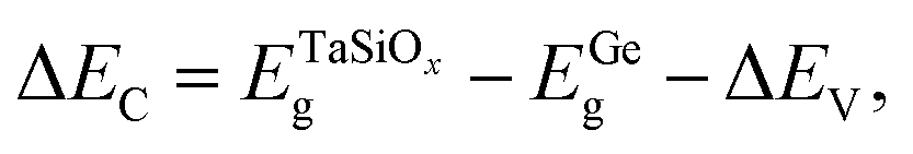
 and EGeg are the bandgaps of TaSiOx and Ge, respectively, and ΔEV is the measured valence band offset. Additionally, the bandgap (Eg) of the as-deposited TaSiOx dielectrics was determined for each crystallographic orientation utilizing the O 1s photoelectron energy loss spectra. Explicitly, the binding energy separation between the “onset” of photoelectron emission (with respect to the spectral background immediately following the O 1s peak) and the center of the fitted O 1s spectral feature(s) provides a direct method in determining an oxide's bandgap. This is due to the nature of dielectric films, which require less energy for band-to-band excitation (i.e., the lowest/principal valence and conduction bands) as opposed to plasmon losses.70 A moderate range of bandgap values, between 4.4 eV–4.65 eV, have been reported in the literature, with variability in the measured bandgap stemming from the deposition method(s) utilized, or empirical method in determining the oxide bandgap (including XPS, photoluminescence and photoemission spectroscopies) of Ta2O5.34–44 Cevro et al.39 reported an optical bandgap varying from 4.3 eV–9.0 eV for x = 1.0 to x = 0.0 atomic mole fraction of Ta2O5 in the composite (Ta2O5)1−x(SiO2)x dielectric. However, Adelmann et al.40 found that for ALD TaSiOx on Si, the bandgap starts to vary from ∼4.5 eV for x = 0.0 up to ∼4.9 eV for x = 0.5.40 As such, a precise determination of the TaSiOxEg is important in order to accurately determine ΔEC at the TaSiOx/Ge heterointerface. Lastly, as discussed in the Experiments section, we note that statistical deviation in the Au 4f7/2 CL BE of a Au standard was utilized in the derivation of a ±0.04 eV experimental uncertainty for this work, from which successive uncertainty was estimated using a root-sum-square approach.78–80