
 Open Access Article
 This Open Access Article is licensed under a Creative Commons Attribution-Non Commercial 3.0 Unported Licence
Review of defect engineering in perovskites for photovoltaic application
Souhardya
Bera
a,
Ankit
Saha
a,
Shibsankar
Mondal
a,
Arnab
Biswas
a,
Shreyasi
Mallick
a,
Rupam
Chatterjee
b and
Subhasis
Roy
 *a
*a
aDepartment of Chemical Engineering, University of Calcutta, 92 A. P. C. Road, Kolkata 00009, India. E-mail: subhasis1093@gmail.com; srchemengg@caluniv.ac.in
bDepartment of Chemical Technology, University of Calcutta, 92 A. P. C. Road, Kolkata 00009, India
First published on 1st June 2022
Abstract
Perovskite-based devices have achieved high efficiencies in the fields of photovoltaics and energy storage. However, intrinsic defects in the deep levels of the perovskite structure are both morphological and structural. Perovskites mainly suffer from extrinsic defects at their interfaces and grain boundaries, ultimately affecting the perovskite film crystallinity. Moreover, they additionally depreciate the band alignment and charge transport. Defect engineering is therefore the ideal option to enhance device performance and stability. The initial substrate formation plays a consequential role in determining the morphology of the structure and different materials can thus be tested as precursors through different initial fabrication strategies to develop quality perovskite films. Composition engineering is also practiced, with dopants added at various levels of fabrication. In some cases, synthesizing defects also improves the device performance with reasonable stability. Herein, categorizing the defects, should be of primary importance given that defect structuring is very important to upgrade the perovskite performance for commercial applications.
1. Introduction
In recent years, the perovskite structure has shown great prospects in photovoltaic cells and energy storage applications, such as in lithium batteries. The perovskite-based photovoltaic cell has a low cost and long lifetime.1–4 These types of solar cells possess desirable features such as tunable bandgap,5 excellent light absorption capacity, long electron–hole diffusion length,6,7 minimal recombination rate,8 and high charge carrier mobility.9,10 Moreover, perovskite solar cells (PSCs) have better power conversion efficiency and greater open-circuit voltage compared to those of dye-based photovoltaic cells.11 PSCs have increased the performance efficiency of photovoltaic cells from 3.9% to 22.7%.12–16Perovskite structures have advantages over conventional semiconductors in that although these materials are processed at lower temperatures, their structures are highly crystalline and can be prepared in various forms such as nanocrystals,17 nanorods,18 nanowires,19 platelets, and microspheres.20 These features make the applications of perovskites versatile, lending themselves to applications in batteries, supercapacitors, solar energy devices, energy-efficient light-emitting diodes (LEDs), and lasers.21
Recently developed solution-processing techniques such as one-step deposition, two-step sequential deposition, and solvent quenching can result in highly crystalline perovskite structures with excellent solar cell performance. Additionally, the basic methylammonium lead iodide perovskite can be engineered into mixed-cation and mixed-anion halide perovskites to increase the stability and efficiency of the perovskite structure.6,22–25
Various defects in the polycrystalline crystal can make the solar cell performance much lower than the theoretically achievable limits.
The perovskite structure in solar cells is susceptible to decomposition due to the weak bonds and lower intrinsic instability. The cations in the organic salts can escape from the crystal structure during the thermal treatment process, which leads to a non-stoichiometric surface on the perovskite crystal. The perovskite crystals synthesized from organic ammonium halide precursors could have some unreacted precursor salt that can lead to hindered transportation and the formation of non-radiative recombination centers. Different methods are implemented to control or eradicate these defects.19,26–29 To control the nucleation and development of the perovskite film and passivate the trap sites, several additives such as alkyl halides, ionic liquids, Lewis bases, alkyl metal cations, fullerene derivatives, and polymers can be doped in the precursor solution. Studies also reveal that the moisture instability perovskite structure faces are usually due to the presence of amine groups in the cation that are usually hygroscopic. A suitable solution to mitigate moisture instability is increasing the number of cations through doping or lowering the dimensions of perovskites. The replacement of MA+ with FA+ has also been suggested for improved thermal stability, although this originates from the basic chemistry of perovskite compounds and cannot be classified as a defect. Thermal stability and moisture stability require major attention for the commercialization of perovskites beyond silicon solar cells.30
Various studies on solid-state batteries have shown that they can be safer, more electrochemically and mechanically stable, and have a longer life cycle,31,32 which is a good alternative to the lithium battery, which has flammable organic liquid electrolytes33–38 Solid-state batteries, like lithium-ion, lithium–air, lithium sulfide, and lithium bromide batteries, have very high energy densities. The solid-state electrolytes used in these batteries are ceramic oxides such as perovskite-based materials (LLTO),39,40 anti-perovskites (LLNO)41,42 and the garnet structure (LLZO).43–55 The grain boundary barriers and moisture sensitivity of this type of solid-state electrolyte hinder the lithium-ion conduction in the entire cell structure, reducing the efficiency of the solid-state cells. These problems combined with the complex chemical reactions reduce the commercial viability of these types of cells.56 Crystal doping can form crystal distortions or create defects in the anti-perovskite structure, which can enhance the lithium–ion mobility through the bulk crystallite.57 The substitution of cations and anions in the crystal structure can also be used to increase lithium–ion conductivity.58–60 Fluorinated lithium-rich anti-perovskite solid-state electrolytes can further escalate lithium–ion conductivity. This can enhance the local microstructure and create Frenkel defects in the crystal lattice, which enhances the lithium–ion conduction.
2. Perovskite structures and defect interpretation
When a large oxide ion and a metal ion with a small radius are combined, it results in a crystal structure that has oxygen ions forming a cubic close-packed lattice structure and the octahedral interstitial sites contain the metal ions. This type of arrangement is mostly observed in crystals of transition metal oxides with a valency of +2. If one of the oxygen atoms is replaced by a cation with a similar radius to that of alkali, alkaline earth, or rare earth elements, then the number of octahedral voids occupied by cations is reduced to one-fourth. This type of ionic arrangement has the general chemical formula ABX3 (where X can be O2−, F− or Cl−). The A atoms are located in the special Wyckoff positions 1b, (1/2, 1/2, 1/2); the B atoms are present at 1a, (0, 0, 0); and the X atoms are present at 3d, (1/2, 0, 0); (0, 1/2, 0); (0, 0, 1/2). With the usual position of the A cation lying in the B–X framework cavity, perovskites provide substantial versatility in tailoring their crystal structure. The general structure of perovskite crystals along with their dipole moment orientations have been listed in Fig. 1.61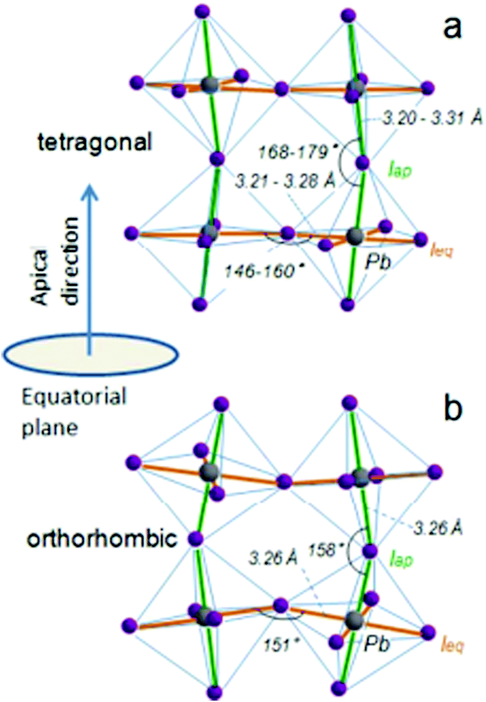 | ||
| Fig. 1 General schematic illustration of the perovskite crystal structure and the proposed dipole moment orientation about the orbital hybridization directions: (a) tetragonal phase and (b) the orthorhombic phases highlighting the Pb–I bond lengths and the Pb–I–Pb bond angles of the equatorial and apical iodide61 [Reprinted with permission. Copyright (2016) American Chemical Society]. | ||
A perovskite-like SrTiO3 has a structure in which Sr2+ and O2− form a close-packed cubic lattice and the Ti4+ ions occupy the octahedral holes that are formed by the oxygen ions. The perovskite consists of a net-like three-dimensional structure in which the octahedral corners share a common [TiO6] and the Sr2+ are present in the twelvefold cavities in between the polyhedral structure.
A perovskite structure that has a vacant (A) position is referred to as the ReO3 type. When the ReO3 structure is converted to a more closely packed hexagonal structure due to the rotation of the octahedral structure, this structure is referred to as the RhF3 structure. In this case, the central void is surrounded by an octahedral structure. An ilmenite structure (FeTiO3) is formed if the central octahedral hole is occupied.
The abovementioned structures can be transformed, in order to validate the flexibility of a standard perovskite structure.
A superstructure that is related to perovskites can be formed if all the three edges of the unit cell are doubled. In this superstructure, equivalent positions can be occupied by different atoms. A one-to-one relation of perovskites with this structure can be established using a doubled formula of that perovskite. In the perovskite superstructure of cryolite (Na3AlF6), the Na+ ion occupies the equivalent positions of Sr2+ and Ti4+. The presence of these different-size ions in different equivalent sites causes some distortion of the crystal structure.
The distortion or defect can be caused by three factors: size effects, deviation from the ideal composition, and the Jahn–Teller effect.
i. Size effects: when a perovskite structure forms an ideal cube with side length ‘a’ and ionic radii rA, rB, and rO, the geometric relationship between them can be represented by the following equation:
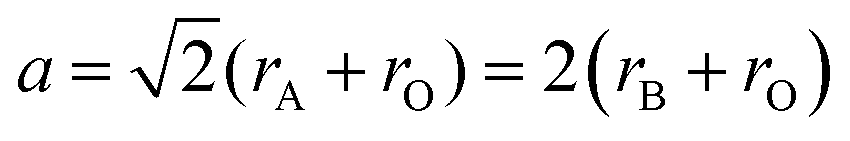 | (i) |
Goldschmidt's tolerance factor (t) is the ratio of these two values of ‘a’. This gives an approximate value of the degree of distortion. Because this factor is based only on ionic bonds, perovskite compounds with a higher degree of ionic bonding can be well applied to this calculation.
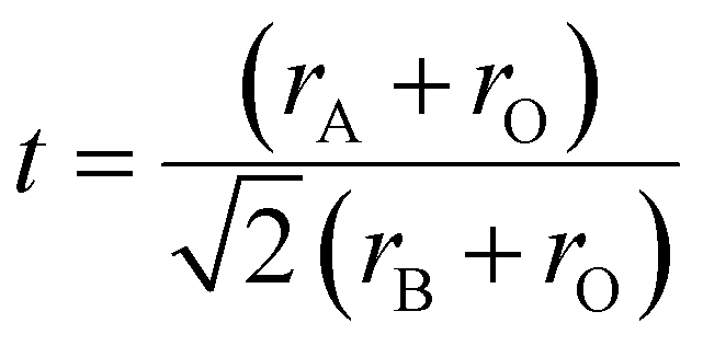 | (ii) |
An ideal perovskite has t = 1. The perovskite structure remains cubic if 0.89 < t < 1. A perovskite structure in which the A ion is smaller than the optimum size and has a value smaller than unity makes the octahedral structure of [BO6] tilt towards one side to cover up space. This defect might make the perovskite structure less stable than the ideal structure. However, ilmenite, which has t < 0.8, has a much more stable structure.
If the A ion is larger or the B ion is smaller than in the ideal structure, this results in a ‘t’ value greater than unity. In this case, the perovskite structure remains hexagonal. The perovskite BaNiO3 has a structure of this type. The BaNiO3 structure consists of a close-packed structure that forms a hexagonal stack and [NiO3] shares a common face in the crystal lattice. The ‘t’ value can only give an estimation of a defect in a perovskite structure since perovskites do not have a fully ionic structure.
ii. Deviation from ideal composition: This type of defect can be observed by changing the composition of the ideal perovskite. For example, the value of x for the perovskite SrFeOx varies between 2.5 and 3. On subjecting this type of perovskite to a reducing or oxidizing environment and heating, the oxidation state of Fe ions fluctuates, with some in the +3 oxidation state while others are in the +4 oxidation state. Fe, which is present as [FeO5], makes the structure into a square pyramid form instead of the ideal cubic form. The composition of these types of perovskites can be given by AnBnO3n−1 where the value of ‘n’ can be 2 to ∞.
iii. The Jahn–Teller effect: according to the Jahn–Teller theorem, any non-linear molecule with a spatially degenerate electronic ground state will undergo a geometric distortion, which will eliminate the degeneracy by lowering the overall energy of the species. Some perovskites have this type of distortion at the B position due to Jahn–Teller active ions.62
The octahedral factor also assesses the stability of the perovskite octahedron BX6− based on the best fit of the B cation in the octahedron. Due to the distortion in the perovskite system, the octahedron deviates from its ideal cubic state, resulting in a variation in the unit cell volume, establishing the tolerance factor as a measure of the extent of distortion in the crystal lattice. Pauling's octahedral factor is usually denoted by 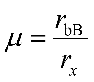 ; however, a plot with ‘t’ can depict the suitability and stability of the perovskite based on both the A cation and B cation, respectively. The B cation must fit in the X6 octahedron, where rB < 0.414 < rx is deemed too small to form a perovskite structure. Hence, with the increasing size of the halide ions, the number of B cations fit to form a stable perovskite is very less; 8, to be exact, for iodide perovskites.63 Based on the Goldsmith tolerance factor and Pauling's octahedral factor, considerable effort has gone into defining a “stability range”, either by proposing boundaries for t and μ or by utilizing machine learning to create t vs. μ curves that enclose the data points. The relevance of these endeavors is that they explore the no-rattling principle's predictive power in qualitative terms. However, these approaches suffer from a heavy reliance on empirical ionic radii. It is commonly acknowledged that the concept of ionic radii is nonunique, with deviations reflected in coordination and local chemistry even within the same definition. The stability ranges suggested thus far are observational rather than predictive, as these uncertainties are transferred to the octahedral and tolerance factors.64
2.1. General perovskite fabrication approaches
The quest for particular features for high efficiency in ultimate application dictates the synthesis of perovskites, as it is known that the crystal structure, surface morphology, and other properties of perovskites are reliant on their synthetic technique. However, among solid-state, solution-state, and gas-state synthesis, solution-state synthesis has a good capacity to create nanomaterials, and is therefore the most widely applied synthetic technique by scientists and the research community. The use of such synthetic methods in the industry is in progress. However, the widespread use of such methodologies while following strict industrial regulations is still a challenge that needs to be addressed by the scientific community to eradicate the costly fabrication techniques of Si-tandem cells.The usual choice of base for perovskite solar cell fabrication is glass panels, although coated glass panels such as laser-etched fluorine tin oxide (FTO) or iodine tin oxide (ITO) can also be used. The base is passed through an ultrasonic bath for approximately 15 minutes, followed by drying in an inert nitrogen atmosphere, and is subsequently treated by UV ozone. It can also be treated using deionized water, acetone, ethyl alcohol, and isopropyl alcohol, followed by intermittent drying and UV ozone treatment.
This cleaned glass is then coated with a thin film of SnO2 or TiO2, which acts as a electron transport layer (ETL) for the perovskite solar cell. A buffer layer of SnO2 or TiO2 can also be applied before this step, which is only done for certain variable enhancements in solar cell performance. This is accomplished by spin coating the glass with a 2% solution of SnO2 or TiO2 and then annealing the glass at 150 °C.
The glass panel is spin-coated twice again with the precursor perovskite salt solution, initially by the precursor salt solution and then by a cation salt added to the precursor salt solution. After the coating process, the glass is annealed at 100 °C. To protect the perovskite film, the glass is spin-coated with a solution of spiro-OMeTAD, which is prepared by dissolving spiro-OMeTAD in a solution consisting of 4-tert-butyl-pyridine, Li-TFSI (dissolved in acetonitrile), FK209CO(III)TFSI salt (in acetonitrile), and chlorobenzene. This coated glass is then again annealed to set the film. Finally, electrodes are added to this perovskite-based solar cell using thermally evaporated silver.65,66 A schematic of such a fully prepared perovskite solar cell has been provided in Fig. 2.67
 | ||
| Fig. 2 A schematic representation of a typical perovskite-based photovoltaic cell67 [Reprinted with permission. Copyright (2018) American Chemical Society]. | ||
2.2. Categorizing general defects
Defects in the perovskite structure can be classified based on their formation types. These defects are caused by atomic vacancies, interstitials, and antisite substitutions, and higher dimensional defects are formed due to dislocations, GBs, and precipitates.Defects can also be segregated into point defects, line defects, planar defects, and bulk defects. The defects formed around a single lattice point are known as point defects. These include vacancy, interstitial, antisite, substitution, Frenkel, Schottky, and substitutional impurities.
Line defects are formed when atoms get misaligned along with a linear defect. This type of defect can be described by Gauss theories. Edge dislocation can be considered a line defect.
Planar defects are formed when a discontinuity is formed across a plane in a perfect crystal structure. A grain boundary defect is a line defect, which affects moisture degradation in perovskite crystals besides affecting ductile cracks in the boundaries. In mitigating this defect, a lower trap density can be ensured, resulting in a decreased recombination rate and thus better performance than its thin-film counterparts.68
Bulk defects or volume defects are formed when several atoms are missing from an internal crystal structure, which leads to the formation of pores or cracks. This defect can also be formed due to the inclusion of impurities in the crystal structure. The precipitate is a bulk defect.
The vacancy defect is formed when some atoms leave their regular position in the crystal lattice due to high thermal fluctuations. This can lead to extra charge in the crystal corresponding to the charge on the leaving atom. Additionally, it reduces the diffusion length and charge-carrier mobility, introducing deep-level trap zones that result in recombination. The schematics of such defects and their scanning tunneling microscopy (STM) images have been provided in Fig. 3![[thin space (1/6-em)]](https://www.rsc.org/images/entities/char_2009.gif) 69 for further illustration. However, the crystal structure remains stable because of the movement of the neighboring atoms, and as a result, the vacancy gets dislocated and moves through the crystal lattice as an ionic hole. This defect can be mitigated by the introduction of halides and halide salts.
69 for further illustration. However, the crystal structure remains stable because of the movement of the neighboring atoms, and as a result, the vacancy gets dislocated and moves through the crystal lattice as an ionic hole. This defect can be mitigated by the introduction of halides and halide salts.
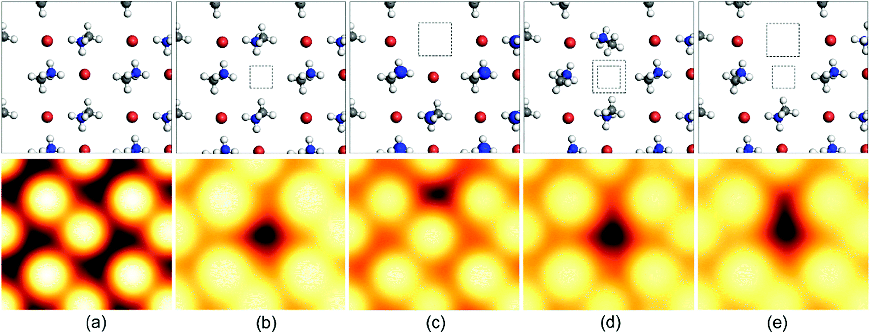 | ||
| Fig. 3 Schematic representation of the top-layer atoms and the simulated scanning tunneling microscopy (STM) images of (a) the pristine CH3NH3PbBr3 (010) surface and a surface with (b) a Br vacancy VBr, (c) an MA vacancy VMA, (d) a Br–Pb double vacancy VBr–Pb, and (e) a Br–MA double vacancy VBr–MA. These STM images were all calculated with a W (111) tip. The squares show the position of the missing Br/Pb atoms or MA cations. Vbias = −3.0 V. Color code: N (blue), C (gray), H (white), Br (brown).69 [Reprinted with permission. Copyright (2017) American Chemical Society]. | ||
An interstitial defect can be formed if an atom that gets dislocated during a vacancy defect moves to an interstitial position in the lattice structure of the crystal. Antisite substitution is formed when a crystal is composed of different atomic species and an atomic species interchanges its position in the lattice structure with another species of the crystal. To mitigate this class of perovskite crystal defects, it is crucial to introduce tri-iodides in FA-based PSCs.
A Frenkel defect is formed in a perovskite crystal structure when an ion leaves its place in the lattice structure and occupies an interstitial site. A general schematic representation of such Frenkel defects has been illustrated in Fig. 4.70 This type of defect in a perovskite material like MAPbI3 can be represented by
| I0I → VI+ + Ii− | (iii) |
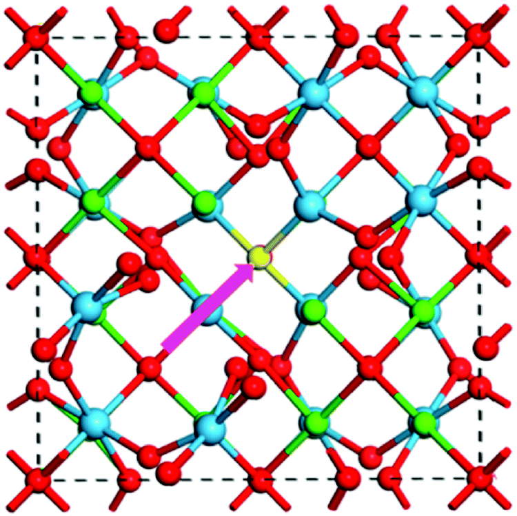 | ||
| Fig. 4 General schematic of the formation path of a Frenkel pair defect (highlighted in pink) in La2Hf2O770 [Reprinted with permission. Copyright (2017) American Chemical Society]. | ||
A Schottky defect is formed when cations and anions leave the crystal lattice in the same stoichiometric ratio, giving rise to vacant sites in the perovskite structure. In Fig. 5,71 a schematic representation of the Schottky defect has been illustrated for further reference. Additionally, there have been reports suggesting the switching behavior of physical sensors, namely Si/SiO2 metal oxide semiconductors (MOSs), which might be attributed to the inherent surface effects.72
| I0I → VI+ + I− | (iv) |
 | ||
| Fig. 5 Schematic representation of a Schottky defect71 [Reprinted with permission. Copyright (2004) American Chemical Society]. | ||
If some impurities are not removed from the perovskite precursor salts, then the impure atoms can replace an original atom from the crystal lattice. This defect is known as a substitutional impurity.
The edge dislocation defect is caused when a plane of atoms terminates abruptly within the three-dimensional crystal structure and does not reach the opposite crystal edge. The adjacent planes bend around the abrupt end of the middle atomic plane. This bend in the adjacent crystal planes makes the atomic planes next to these two adjacent planes be in perfect order.
A grain boundary defect is caused when a crystal structure contains different crystalline orientations and the planes at which these different orientations meet to form a grain boundary. The grain boundaries are not perfectly crystalline. This defect is caused when there is uneven crystal growth during crystallization.
A precipitate is formed when there is more impurity in the perovskite precursor salt and this impurity forms its crystal structure or forms small clumps of precipitate as inclusions inside the main crystal.
3. Defects of perovskites in photovoltaic applications
One of the major reasons why the applications of perovskites have increased multifold in the last decade is due to their tunable bandgap that can range from the infrared region to the ultraviolet. As a competitive edge over their counterparts in third-generation solar cells, i.e., DSSCs, from which they have evolved, these classes of perovskite halides usually provide carriers for absorbing light, which requires the distributed excitation dissociation interface seen in a DSSC. Although their efficiency has skyrocketed in recent years, it is understandable that deep-level imperfections in perovskite thin films are preventing the PCE from approaching the theoretical Shockley–Queisser limit. Due to the high density of deep-level traps that trap either electrons or holes and do not escape by thermal recombination, Shockley–Read–Hall (SRH) statistics are a significant loss mechanism that gives the rate of non-radiative recombination process in perovskites.73,74 Transparent conductive oxide (TCO) makes up the top layer, which aids in the decay of the photo-excited population through contact. This takes place when the excitation density is low. Below this layer is a three-layer sandwich, with perovskite being the middle layer. The perovskite layer forms a heterojunction with the top and bottom layers. The top and bottom layers have a wide bandgap and there is also a selective carrier. Below the bottom layer, there is a metallic back contact, which is usually formed by nano-deposited silver.12,24,75–77The absorption coefficient of the perovskite layer is approximately 104–105 cm−1,78 which can absorb most of the incident light. The thickness of the layer is about 300–500 nm and the reflective back contact also reflects the radiation, which does not get absorbed in the first pass.79 The grain growth and optoelectronic properties of the fabricated perovskite film are influenced by factors such as the perovskite precursor ratio, additives used during solvent processing, substrate roughness and surface energy, atmospheric and environmental conditions, annealing temperature and treatment time.80 When the photo-excitation density is very high, the probability of interaction among the three layers also increases, which can lead to Auger recombination, which becomes a defect in a perfect crystal structure. The defects can be categorized as point defects (e.g., atomic vacancy defect), interstitials, antisite substitution, and higher dimensional defects.81,82 When the formation energy of a defect in a perovskite turns negative, which is determined by the atomic chemical potential and the electronic chemical potential, the defect becomes thermodynamically favorable. Additionally, the atomic chemical potential is affected by the concentration and activity of the reactants.83–86 The Fermi level, on the other hand, determines the electronic chemical potential, which indicates that the conditions maintained during crystal development affect the defect formation in the crystal interior.28,87–90 The theoretical calculation of the energies of formation can give an estimate of the defects in the crystal structure. When a systematic defect analysis of the material is required, the energy of formation is calculated for different charge states, and the charge state with the lowest energy requirement is generally considered the most stable state. This charge state, which is considered the most stable, also depends on the Fermi level.16,91–107
The most prevalent types of defects in perovskite halides are point defects, and the perovskite methylammonium lead iodide (CH3NH3PbI3), which is commonly used in photovoltaic applications, possesses as many as 12 varieties of native point defects. The defects in this perovskite are studied theoretically by calculating the energies of formation in a host crystal when its crystal is at equilibrium with its precursors. This study gives an estimate of the types of defects and favorable growth conditions. Iodide vacancies and interstitials can easily diffuse across the perovskite crystal and interfaces, according to Azpiroz et al., with migration activation energies as low as ∼0.1 eV, although the slow response time of PSCs could not be attributed to the migration of ion defects alone.108 Density functional theory (DFT) has been used to determine the calculated quantities. Studies have shown that if point defects are present in CH3NH3PbI3, then there would be deep levels in the bandgap when the energy of formation is high and the point defects will also contribute to a shallow state. According to this assumption, there should not be non-radiative recombination centers present at high densities when point defects are present, since these lie deep within the bandgaps. However, experiments show that there are exceptions to this general assumption. This is because there is the formation of covalent bonds between atoms that are present around the defects and these are present at much deeper locations in the bandgaps. The shallower point defects can contribute to unintentional doping even at room temperature. VMA and VPb are the acceptor defects and VI is the donor defect. These shallow donor and acceptor defects (the 3 defects that have energy levels less than 0.005 eV above the valence band maximum) occur when the energy of formation is lower and p- and n-type doping can be done in these defects. When stoichiometric growth conditions are maintained, the Schottky disorder type defect is more common than the other types of point defects. Though the energy of formation is lower in the case of the Schottky defect, there is less chance of accidental doping as there is a charge carrier for each vacant site. Significant first-order recombination is caused by structural Schottky defects, such as halide vacancies at grain boundaries, resulting in low VOC and a substantial light-harvesting effect.100,109 Because of their inherently high trap densities, perovskite films with many grain boundaries are susceptible to first-order recombination. Compact perovskite films, on the other hand, have a substantially lower trap density and less first-order recombination than bulk films. Charge trapping or accumulation at the perovskite/charge transport material interfaces is also caused by imperfections on the surface of the HTL or ETL. Grain boundary and surface defects, such as defect arrays, undercoordinated ions of terminating lattice periodicity, and combinations of point defects and dislocations on crystal surfaces and interfaces, are frequently categorized under two-dimensional (2D) defects. According to Meggiolaro and colleagues, ion migration in metal halide perovskites is dominated by surfaces and grain boundaries due to surface-assisted defect generation; and surface passivation plays a key role in stabilizing lead halide perovskites against defect formation. This may prevent the photochemical breakdown events that are associated with this class of materials, offering a foundation for understanding their strange ion conduction properties and light-induced instability.110 Phung et al. studied the kinetics and mechanism of ion migration using photoluminescence microscopy. Migrating iodide and perhaps methylammonium ions are likely to saturate the created and available vacancies, resulting in a shift in the PL yield. At the same time, the removal of ions from their crystalline positions reduces the PL yield, introducing non-radiative recombination centers. The recovery of PL supports the idea that defects can be trapped near grain boundaries and then move back to faulty crystalline sites to “repair” the lattice once the excitation is turned off, which was further confirmed by molecular simulations.111
The photoactive phase can be made from monovalent cations that have a Goldschmidt tolerance number in the range of 0.08–1. However, it has been observed that MA+ cations can leave the crystal when subjected to heat or light. This can be avoided by substituting MA+ with monovalent cations having a smaller atomic radius than MA+ (e.g., Rb+, K+, Na+). However, cations smaller than Cs+ can accumulate at grain boundaries or interstitial positions without serving as a replacement for inorganic or organic cations. This can lead to an increase in grain size. Additionally, the monovalent cation K+, which has an optimum cation:anion ratio, can form a Frenkel defect by dislodging into the interstitial spaces. The accumulated K+ ions at the grain boundaries and on the surface make the excess halide inert and immovable by forming bonds with the same. This leads to the self-passivation of the perovskite. The defect tolerance of various lead halide perovskite compositions and the types of defects that commonly occur in halide perovskites were investigated by Ye et al. Their review article also included an overview of surface passivation procedures for colloidal NCs and thin films to increase their optical properties and, as a result, the efficiency of the resultant LEDs and solar cells.112 Saykar et al. focused on interface, additive, and gradient band alignment engineering in their review work, and the resulting increase in photocurrent density, photovoltage, power conversion efficiency, and long-term stability that occurred.113
Lithium lanthanum titanium oxide perovskite materials have been shown to inherently exhibit relatively good electrochemical applications and high conductivity. In the literature, sodium ion conduction has been studied for the interlayer planes of Ruddlesden–Popper (RP) layered perovskites.114–116 The ion transport within the perovskite layers in the required LLTO structures has not been extensively studied.117,118 However, in an investigation by Lin et al., they studied the defect engineering strategies to induce Na deficiencies for the formation of the required phase.119 Similar to LLTO,48–51 other available materials that have found extensive attention are LLNO,52–54 anti-perovskite, and garnet-structured LLZO58–60,62 due to their substantial electrochemical stability and higher conductivity, which has rendered them suitable for industrial applications in batteries. In a work by Hong et al., they studied different defects occurring in the quenching process of LLNO. Additionally, it can be inferred from their study that specific defect engineering can be a method to enhance the ionic conductivity and applicability of LLNO in solid electrolyte batteries120
3.1. Effects on the performance of photovoltaic cells
As already mentioned, the Shockley–Queisser PEC (photoelectrochemical) limit of perovskite-based solar cells cannot be approached by metal halide perovskites due to the presence of deep defects in the film. The defects at the grain boundaries and inside the grain structure that are formed due to the solution-processed polycrystalline perovskite-forming approach, can lead to very rapid non-radiative decay and is suspected that this can lead to the degradation of the perovskite film.121,122 It should also be noted that the limit is defined by certain assumptions, specifically relating to the spectral and equilibrium state. The intrinsic structural defects cause the equilibrium state to create unavoidable radiative charge recombination of electron–hole pairs, but studies indicate that non-radiative charge recombination is avoidable and should be eliminated. Luo et al. investigated the most common general routes for non-radiative recombination losses in PSCs and assessed their on-cell performance.123 Defect-mediated carrier recombination is especially important for understanding solar cell performance. since at times, it tends to decrease the steady-state charge density. This decreases the gap between quasi-Fermi levels, which dictates the VOC. Surface recombination is also prominent in PSCs without HTL, where the fabricated devices suffer from high defect-recombination. With an optimized and higher VOC and a bandgap as the activation energy for recombination, it can be deduced that defect recombination occurs in the intrinsic bulk of the absorber layer.124If an ionic defect is present in a perovskite, this will lead to accumulation or depletion at the grain boundaries in an imbalanced manner. This will lead to upward (for electron transport) or downward (for hole transport) bending of the band and will help to separate the electronic charge carriers or impede their movement. This shows the sensitivity of the optoelectronic property of the grain boundary to defects. The ionic defects can be quantified and characterized by their atomic densities, which requires us to understand the basic ideas behind crystal structure, crystallographic orientation, and chemical composition.125 In addition, understanding the phenomenon of ion migration is crucial for the performance characterization of perovskite-based PV cells.
If impurity-based defects are present, it can lead to the formation of recombination centers. This can lead to SRH non-radiative recombination centers. This will mainly affect the VOC (open circuit voltage) by decreasing the lifetime and photovoltaic performance. This is because the trap-assisted recombination rate will decrease and higher voltages will be reached within the lattice before recombination takes place to cancel out the photocurrent completely.
The VOC can be expressed in terms of non-radiative voltage loss (ΔVnonradiOC) by the following equation:126
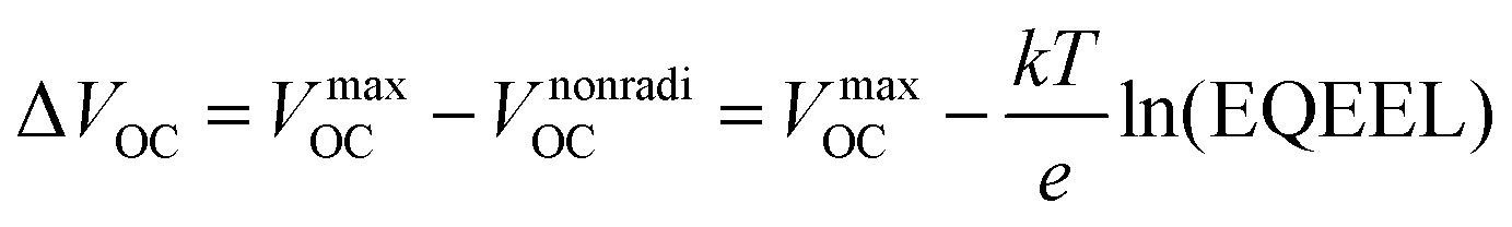 | (v) |
The defects present in the perovskite film and on the surface cause the anomalous current density–voltage (J–V) hysteresis of the perovskite solar cell. The defects in the perovskite film provide a favorable path that causes the migration of ions because of steric hindrance. The charge traps, which are caused by the inductive effect of the defects, when subjected to forward bias, get filled up and get discharged during short-circuit conditions. As a result, these charging and discharging cycles lead to the hysteresis behavior of the perovskite-based solar cell.
The work done by Park and co-workers indicates that the hysteresis behavior can also be caused due to the presence of Frenkel defects. Frenkel defects are caused when the iodide ions migrate to the OH interstitial spaces.127
Several research works have shown that grain boundaries are most susceptible to degradation since these provide sites for charge accumulation and provide a pathway for the infiltration of moisture. Identifying the reasons for instability and the mechanisms that cause it has become a primary concern. Electronic defects in perovskites play an essential role in the deterioration of PSCs, and can come from a variety of sources. However, there might not be any noticeable effect of defects on photocurrent output. Unexpectedly, the degraded device performance caused by the presence of defects has been sometimes seen to be partially reversed within minutes, revealing that more research into the relationship between defects and device stability is recommended.128 The thermal stability of hybrid PSCs is also controlled by the interfacial contact and charge transport layers, specifically by changes in the electrical and physical properties caused by heating.129 The charge transfer dynamics and charge recombination process, which determines the performance of hybrid PSCs, have been demonstrated to be highly dependent on the energy-level alignment at those interfaces. The lack of an energy barrier at the perovskite/interfacial layers allows for easier charge transfer and lower charge recombination. The energy barrier, on the other hand, prevents charge transfer and causes significant charge carrier recombination losses. A study by Choi and co-workers has shown that in the simultaneous presence of accumulated charge and moisture, the perovskite starts to degrade along the grain boundaries. Initially, the instability was attributed to the hydrolysis of the amine compound, with first-principles calculations suggesting that the deprotonation of MA+ with H2O was the principal cause. However, more studies in the field have revealed that at moderate humidity, MA+ cation perovskites readily turn into monohydrates, and at high humidity, they turn into dihydrates. Additionally, metal electrodes can be corroded by ion migration, which is related to the defects. This electron corrosion has been observed in silver electrodes because the activation barrier for iodine ions is 0.1–0.3 eV, which is close to that of silver. These iodine ions are deposited as an inert film on the electrode surface, which deteriorates the performance of the solar cells.130
3.2. Defect engineering of the perovskite structure for photovoltaic application
The doping of perovskite halides with a low concentration of Al3+ can reduce the number of defect sites and minimize microstrains in the crystal lattice. The charge level also decreases from 13.09 to 12.64 meV in this case, which is indicative of the reduction in disorder within the crystal lattice. This in turn, helps to improve the electronic quality of the perovskite lattice.16,107When the perovskite halide is doped with monovalent cation halides in which the cations have radii comparable to that of Pb2+ (Cu+, Na+, Ag+), the surface of the perovskite and the grain boundaries can be made passive. Cd2+, which has the same valency as Pb2+ but a smaller ionic radius, can be incorporated into the perovskite to stabilize its structure. Structural stabilization occurs in this case because of the decrease in the lattice strain and increase in the energies of formation of the vacancies. The doping of the perovskite with Ni2+ has been shown to make the antisite defects in PbI3 passive and increase the crystal order and grain size, which in turn increases the lifetime of PL from 285 to 732 nm. The performance of perovskite-based tandem solar cells can be increased if the cation composition is engineered in such a way that the VOC value is lowered over a wide range.84,86,131,132 In Fig. 6,133 such an illustration has been provided with an increased focus on the filling of I− and MA+ vacancies by FAI post-treatment. The MA+ cation, which has a strong dipole moment, can be added to the mixed-cation–halide-based perovskite to decrease the number of deep trap defects and remove the defects in the wide bandgap.
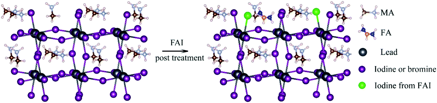 | ||
| Fig. 6 Schematic illustration of the filling of I− and MA+ vacancies in the perovskite films by the FAI post-treatment process133 [Reprinted with permission. Copyright (2018) American Chemical Society]. | ||
Mixed-cation perovskite defects can also be mitigated by exposure to light. This is termed as photo-induced passivation, and can be used to remove bulk defects. This also increases the lifetime of the perovskite material. The addition of excess PbI2 can help suppress non-radiative charge recombination, which will lead to an increase in EQEEL and a decrease in the ΔV (non-radiative voltage loss). Gratzel and co-workers added triiodide ions and found that they help to reduce the deep level defects that are caused by interstitial Pb (PbI) and antisite defects (MAI, PbI, IMA). As a result, the power conversion efficiency (PCE) of 22.1% was obtained.
A study by Huang and co-workers has shown that if fullerene is deposited on the surface of the perovskite film, the trap density reduces and the hysteresis caused by the photocurrent gets reduced.95 A report by Park and co-workers has shown that the Frenkel defect caused by the migration of iodide ions can be mitigated by doping with KI.116
Silver electrode degradation by the migration of iodine ions can be eradicated if an amide-mediated titanium suboxide layer is integrated into the electrode. This layer forms a chemical inhibitor layer and protects the silver electrode from iodine ions.84,86
The stability of solar cells has always been observed to improve following interfacial engineering, regardless of the type of solar cell configuration, the type and duration of the stability or the organic molecule deployed, as per the literature. Interfacial engineering of the substrate on which the perovskite film is formed has demonstrated significant success in controlling the active layer morphology, among other factors. The surface energy of the interfacial layers present at the bottom influences the wetting of the perovskite solution on the substrate, the crystallization, and the morphology of the perovskite by affecting the number of crystallization nuclei and the spacing between the adjacent nuclei, thus specifying the grain size and grain boundaries of the final perovskite film during the film-formation process. It can be evident from the device structure of high-performing solar cells that there are four interface layers: the perovskite/ETL interface, perovskite/HTL interface, ETL/cathode interface, and HTL/anode interface. Furthermore, independent of the interface being adjusted, there is an inherent improvement in stability. As discussed in the previous section, the inherent defects in PSCs have a relatively adverse effect on their overall efficiency. However, defect engineering is effective at inhibiting defects in perovskite materials and at interfaces, with amplified effects on the PCE and stability of subsequent photovoltaic devices. Finding engineering strategies to minimize flaws, such as novel additives, passivation layers, and post-treatment processes, is critical, but it is even more crucial to understand these defects’ potential explanations.134 According to our perspective, having a good grasp of the defect type, defect concentration, and defect distribution will be crucial in determining how to effectively mitigate these faults and develop new PSCs. Specific interactions with halide ions at the interface have been seen to reduce the density of states at the interface, inherently tuning the bandgap of the perovskite material. However, molecular functionalization has been seen to improve the performance of organic–inorganic halide 2D/3D perovskites, subsequently exhibiting hydrogen-to-halogen bonding.135 Greater open-circuit voltages are also associated with the careful modulation of the crystallinity and energy disorder at such interfaces.131 Crystal impurities in FA-based perovskites have been seen to widen the bandgap, which has been addressed by phase impurity management. A direct effect can be seen in the enhancement of carrier lifetimes and VOC, with inherent suppression of hysteresis.136 The correct assessment of bulk and interfacial defects that cause non-radiative recombination and affect band alignment is one of the major gaps in our current understanding.
The relatively high temperature used in solution processing often generates rapid perovskite crystal formation, resulting in a wide spectrum of faults and severely limiting the performance of PSCs. To passivate bulk defects, both positively charged metal ions and negatively charged anions were added to the perovskite precursor solution. Metal cations target undercoordinated halide ions, halide interstitials, and negatively charged Pb-halide antisite replacements (PbX3−), while anions target the defects of Pb interstitials and halide vacancies through ionic contact. In addition to halide ions, anionic groups have been used as ionic bonds to passivate halide vacancies. Although defect-free perovskites should have stoichiometric atomic ratios, the grain boundaries of perovskites with an excess or deficiency of PbX2 can be self-passivated by unreacted PbX2 or organic halides. The insertion of non-stoichiometric PbI2 and organic halide ratios in the perovskite precursor solution has been attempted to passivate grain boundaries.138,139 To address the problem of environmental stress at grain boundaries, additive engineering using zwitterions, Lewis acids (e.g., fullerene derivatives), Lewis bases (e.g., O-donor, S-donor, and N-donor), quantum dots, and ionic liquids have been widely reported to passivate grain-boundary defects, modulate perovskite crystallization and morphology, and improve PSC operation stability.137 In Fig. 7,137 a schematic showing the defect passivation strategies has been listed for further illustration.
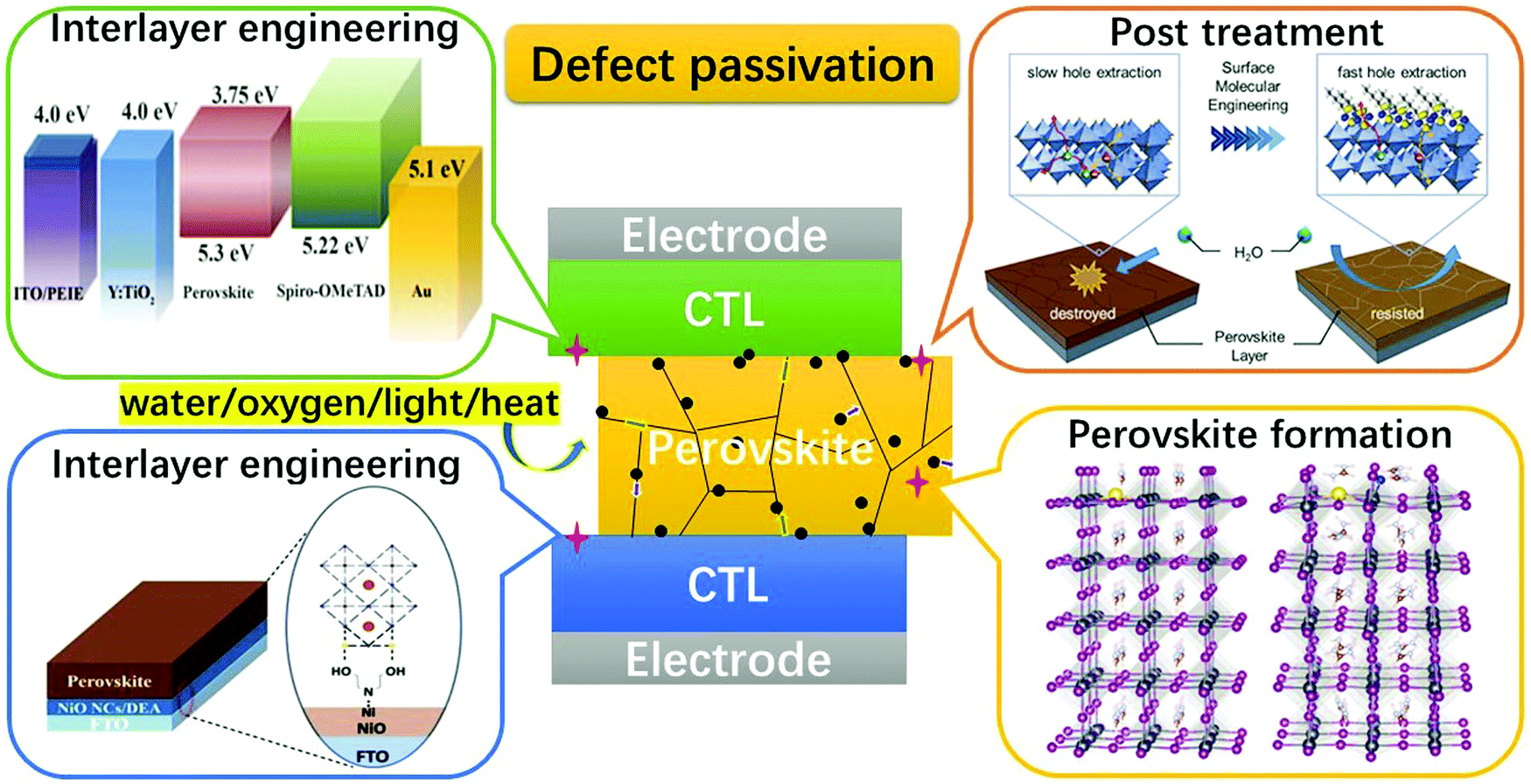 | ||
| Fig. 7 Schematic showing the general defect passivation strategies for PSCs [Reproduced from Royal Society of Chemistry].137 | ||
4. Future perspectives towards defect engineering in perovskite structures
The use of perovskite material in photovoltaic cells and energy storage applications has shown a significant improvement in the efficiency and performance of perovskite devices. However, there are certain issues (such as poor stability, the problem of hysteresis, and the working mechanisms of the defects) that have to be addressed before the perovskite-based devices become marketable. The thermodynamic limit of perovskite-based photovoltaic cells can be approached by contracting the defect density. Various methods have been considered for the passivation of the defects in the crystal lattice. One such prominent approach is to use 2D perovskites to modify 3D perovskites. This approach can significantly decrease the defect density not only in the film but also at the interface. This increases the crystallinity of the perovskite, thus reducing the recombination loss significantly. Such 2D–3D perovskites show enhanced performance and are also easily reproducible. The perovskite can be engineered to increase the grains, improve the film morphology and crystallinity, and gain better control of the defects. This will increase the perovskite stability and also enhance the device performance. Polycrystalline perovskites have a tendency for defect formation. An approach for reducing these defects is to fabricate single-crystalline perovskite films. The problem with this type of perovskite is controlling the thickness of the film and use an appropriate carrier transfer medium. Another advancement in PEC is the development of flexible perovskites. This is because the technology is still in the incipient phase. This technology can be improved by implementing suitable electrodes and flexible substrates. Better control over the defects of perovskites is only possible if we understand both the reasons why defects are generated within the crystal and the tentative method of fabrication used to process the perovskite structure. To implement perovskites in energy storage applications, they need to be corrosion resistant and should have good electrical conductivity. Perovskite oxides must be studied thoroughly using molecular orbital theory or by DFT calculations to get a good understanding of the design principles to be applied. The microstructures present in the perovskite oxides used as the electrodes have to be studied to understand the mechanism of formation of Li2O2, since this compound has low electronic conductivity, which affects the triple-phase boundary among oxygen, lithium ions, and electrons. This results in a low capacity of discharge and the generation of high charge over-potential. Another evolving approach is the use of perovskite oxides in the form of composites. These can be engineered so that the reaction and transport kinetics can be improved.5. Conclusion
In recent years, studies have shown a meteoric rise in the efficiency of perovskite-based devices over that of conventional light-harvesting devices. PSCs can be fabricated at lower temperatures and at a lower cost as compared to conventional PV cells. Perovskite-based devices pose a problem since their stability for long-term usage has to be improved. In the literature, there have been several reports validating the rise of a new class of sustainable light-harvesting devices. In this paper, we have cited most of these works that have contributed to the already existing literature, and as a result, have improved the standard of solar cell research. Graetzel and co-workers have shown that the addition of excess iodine can remove deep level defects. The studies conducted by Park and co-workers have shown procedures for removing Frenkel defects from the perovskite lattice. A study by Choi and co-workers has brought forth methods that can be implemented for protecting the electrodes from internal corrosion caused due to the defects in the perovskite. Quantifying the defects in the grain size and grain boundaries remains a popular research topic to minimize the losses at the interface. Defect engineering can be an essential tool to mitigate the problem of attaining higher VOC and PCE, which in turn increases the commercial feasibility of the solar cells. This paper solely outlines the various defects that can occur in the perovskite crystal lattice, their possible reasons and the methods to minimize or remove these defects. The elimination of all non-essential recombination pathways to attain the highest efficiency is still a problem for the applications of photovoltaics. There have been significant attempts in recent years to advance passivation techniques to increase carrier extraction and stability and reduce non-radiative carrier recombination. In addition, chemical modification, additives, photo-curing, larger grain size, or other appropriate techniques are necessary to achieve high crystallinity and low defect density in perovskite films. Finally, post-treatment is critical for minimizing surface dangling bonds that occur during the film development process. The types of defects, their concentration in the crystal lattice, and their distribution must be studied thoroughly as a proper and thorough understanding of these defects will enable us to find appropriate solutions to eradicate them. The use of perovskites in energy storage applications has shown promising results, especially as electrodes in fuel cells and air batteries as well as electrolytes in solid-state lithium-ion batteries. As a result, the aspect of defect engineering may tune these novel materials for an even better understanding of their light-harvesting properties and enhance their performance characteristics by optimizing their inherent surface and interface morphology, respectively.Author contributions
All authors have contributed equally to this work.Conflicts of interest
There are no conflicts of interest to declare.Acknowledgements
This work was supported by the Science and Engineering Research Board (SERB) grants funded by the Department of Science and Technology (DST), Central Government of India, through the Teachers Associateship for Research Excellence (TAR/2018/000195). The authors would like to acknowledge Dr Achintya Singha, Professor, Department of Physics Main Campus Bose Institute Kolkata, for his valuable comments and ideas, which helped to improve the manuscript. The authors would also like to acknowledge the Department of Science and Technology (DST), Ministry of Science and Technology, Government of India funded project under the MI IC#5 ‘Conversion of Sunlight to Storable fuels’ issued by DBT-DST Joint Funding Opportunity, Central Government of India through the Mission Innovation Programme DST (DST/TMD(EWO)/IC5-2018/06) for providing financial support.References
- R. F. Service, Science, 2016, 354, 1214–1215 CrossRef CAS PubMed.
- A. Moyez and S. Roy, J. Nanopart. Res., 2017, 20, 5 CrossRef.
- S. Roy and G. G. Botte, RSC Adv., 2018, 8, 5388–5394 RSC.
- H. Lu, B. He, Y. Ji, Y. Shan, C. Zhong, J. Xu, J. LiuYang, F. Wu and L. Zhu, Chem. Eng. J., 2020, 385, 123976 CrossRef.
- J. H. Noh, S. H. Im, J. H. Heo, T. N. Mandal and S. I. Seok, Nano Lett., 2013, 13, 1764–1769 CrossRef CAS PubMed.
- Z. Xiao, Q. Dong, C. Bi, Y. Shao, Y. Yuan and J. Huang, Adv. Mater., 2014, 26, 6503–6509 CrossRef CAS PubMed.
- K. Wu, Y. Chen, J. Cheng and K. Xu, J. Appl. Phys., 2020, 128, 173104 CrossRef CAS.
- N. K. Noel, S. D. Stranks, A. Abate, C. Wehrenfennig, S. Guarnera, A.-A. Haghighirad, A. Sadhanala, G. E. Eperon, S. K. Pathak, M. B. Johnston, A. Petrozza, L. M. Herz and H. J. Snaith, Energy Environ. Sci., 2014, 7, 3061–3068 RSC.
- H. Oga, A. Saeki, Y. Ogomi, S. Hayase and S. Seki, J. Am. Chem. Soc., 2014, 136, 13818–13825 CrossRef CAS PubMed.
- C. Wehrenfennig, G. E. Eperon, M. B. Johnston, H. J. Snaith and L. M. Herz, Adv. Mater., 2013, 26, 1584–1589 CrossRef PubMed.
- S. Bera, D. Sengupta, S. Roy and K. Mukherjee, J. Phys. Energy, 2021, 3, 032013 CrossRef CAS.
- A. Kojima, K. Teshima, Y. Shirai and T. Miyasaka, J. Am. Chem. Soc., 2009, 131, 6050–6051 CrossRef CAS PubMed.
- M. A. Green, A. Ho-Baillie and H. J. Snaith, Nat. Photonics, 2014, 8, 506–514 CrossRef CAS.
- S. S. Roy, G. S. Han, H. Shin, J. W. Lee, J. Mun, H. Shin and H. S. Jung, J. Nanosci. Nanotechnol., 2015, 15, 4516–4521 CrossRef CAS PubMed.
- M. Lira-Cantú, Perovskite solar cells: Stability lies at interfaces, Nat. Energy, 2017, 2, 17115 CrossRef.
- A. Moyez and S. Roy, Sol. Energy Mater. Sol. Cells, 2018, 185, 145–152 CrossRef.
- W. Zhang, G. E. Eperon and H. J. Snaith, Nat. Energy, 2016, 1, 16048 CrossRef CAS.
- F. Zhou, Z. Ren, Y. Zhao, X. Shen, A. Wang, Y. Y. Li, C. Surya and Y. Chai, ACS Nano, 2016, 10, 5900–5908 CrossRef CAS PubMed.
- J.-W. Lee, H.-S. Kim and N.-G. Park, Acc. Chem. Res., 2016, 49, 311–319 CrossRef CAS PubMed.
- Z. Xiao, R. A. Kerner, L. Zhao, N. L. Tran, K. M. Lee, T.-W. Koh, G. D. Scholes and B. P. Rand, Nat. Photonics, 2017, 11, 108–115 CrossRef CAS.
- H. Zhu, Y. Fu, F. Meng, X. Wu, Z. Gong, Q. Ding, M. V. Gustafsson, M. T. Trinh, S. Jin and X.-Y. Zhu, Nat. Mater., 2015, 14, 636–642 CrossRef CAS PubMed.
- L. M. Herz, Annu. Rev. Phys. Chem., 2016, 67, 65–89 CrossRef CAS PubMed.
- R. Mishra, S. Bera, R. Chatterjee, S. Banerjee, S. Bhattacharya, A. Biswas, S. Mallick and S. Roy, Appl. Surf. Sci., 2022, 9, 100241 CrossRef.
- M. Saliba, T. Matsui, J.-Y. Seo, K. Domanski, J.-P. Correa-Baena, M. K. Nazeeruddin, S. M. Zakeeruddin, W. Tress, A. Abate, A. Hagfeldt and M. Grätzel, Energy Environ. Sci., 2016, 9, 1989–1997 RSC.
- L. K. Ono, E. J. Juarez-Perez and Y. Qi, ACS Appl. Mater. Interfaces, 2017, 9, 30197–30246 CrossRef CAS PubMed.
- X. Zheng, B. Chen, J. Dai, Y. Fang, Y. Bai, Y. Lin, H. Wei, X. C. Zeng and J. Huang, Nat. Energy, 2017, 2, 17102 CrossRef CAS.
- M. Abdi-Jalebi, Z. Andaji-Garmaroudi, S. Cacovich, C. Stavrakas, B. Philippe, J. M. Richter, M. Alsari, E. P. Booker, E. M. Hutter, A. J. Pearson, S. Lilliu, T. J. Savenije, H. Rensmo, G. Divitini, C. Ducati, R. H. Friend and S. D. Stranks, Nature, 2018, 555, 497–501 CrossRef CAS PubMed.
- J. Xu, A. Buin, A. H. Ip, W. Li, O. Voznyy, R. Comin, M. Yuan, S. Jeon, Z. Ning, J. J. McDowell, P. Kanjanaboos, J.-P. Sun, X. Lan, L. N. Quan, D. H. Kim, I. G. Hill, P. Maksymovych and E. H. Sargent, Nat. Commun., 2015, 6, 7081 CrossRef CAS PubMed.
- C.-C. Zhang, M. Li, Z.-K. Wang, Y.-R. Jiang, H.-R. Liu, Y.-G. Yang, X.-Y. Gao and H. Ma, J. Mater. Chem. A, 2017, 5, 2572–2579 RSC.
- H. Xiang, P. Liu, W. Wang, R. Ran, W. Zhou and Z. Shao, Chem. Eng. J., 2021, 420, 127599 CrossRef CAS.
- A. Manthiram, X. Yu and S. Wang, Nat. Rev. Mater., 2017, 2, 16103 CrossRef CAS.
- E. Quartarone and P. Mustarelli, Chem. Soc. Rev., 2011, 40, 2525 RSC.
- K. Takada, Acta Mater., 2013, 61, 759–770 CrossRef CAS.
- Y. Wang, W. D. Richards, S. P. Ong, L. J. Miara, J. C. Kim, Y. Mo and G. Ceder, Nat. Mater., 2015, 14, 1026–1031 CrossRef CAS PubMed.
- C. Jiang, H. Li and C. Wang, Sci. Bull., 2017, 62, 1473–1490 CrossRef CAS.
- L. Fan, S. Wei, S. Li, Q. Li and Y. Lu, Adv. Energy Mater., 2018, 8, 1702657 CrossRef.
- J. Li, C. Ma, M. Chi, C. Liang and N. J. Dudney, Adv. Energy Mater., 2014, 5, 1401408 CrossRef.
- T. Famprikis, P. Canepa, J. A. Dawson, M. S. Islam and C. Masquelier, Nat. Mater., 2019, 18, 1278–1291 CrossRef CAS PubMed.
- H. Zhang, C. Li, M. Piszcz, E. Coya, T. Rojo, L. M. Rodriguez-Martinez, M. Armand and Z. Zhou, Chem. Soc. Rev., 2017, 46, 797–815 RSC.
- Y. Zheng, J. Wang, B. Yu, W. Zhang, J. Chen, J. Qiao and J. Zhang, Chem. Soc. Rev., 2017, 46, 1427–1463 RSC.
- L. Chen, Y. Li, S.-P. Li, L.-Z. Fan, C.-W. Nan and J. B. Goodenough, Nano Energy, 2018, 46, 176–184 CrossRef CAS.
- B. Liu, Y. Gong, K. Fu, X. Han, Y. Yao, G. Pastel, C. Yang, H. Xie, E. D. Wachsman and L. Hu, ACS Appl. Mater. Interfaces, 2017, 9, 18809–18815 CrossRef CAS PubMed.
- Z. Zhang, Y. Zhao, S. Chen, D. Xie, X. Yao, P. Cui and X. Xu, J. Mater. Chem. A, 2017, 5, 16984–16993 RSC.
- K. (Kelvin), Fu, Y. Gong, G. T. Hitz, D. W. McOwen, Y. Li, S. Xu, Y. Wen, L. Zhang, C. Wang, G. Pastel, J. Dai, B. Liu, H. Xie, Y. Yao, E. D. Wachsman and L. Hu, Energy Environ. Sci., 2017, 10, 1568–1575 RSC.
- D. Lei, K. Shi, H. Ye, Z. Wan, Y. Wang, L. Shen, B. Li, Q.-H. Yang, F. Kang and Y.-B. He, Adv. Funct. Mater., 2018, 28, 1707570 CrossRef.
- L. Wang, Y. Wang and Y. Xia, Energy Environ. Sci., 2015, 8, 1551–1558 RSC.
- Z. Chang, X. Wang, Y. Yang, J. Gao, M. Li, L. Liu and Y. Wu, J. Mater. Chem. A, 2014, 2, 19444–19450 RSC.
- X. Gao, C. A. J. Fisher, T. Kimura, Y. H. Ikuhara, A. Kuwabara, H. Moriwake, H. Oki, T. Tojigamori, K. Kohama and Y. Ikuhara, J. Mater. Chem. A, 2014, 2, 843–852 RSC.
- X. Gao, C. A. J. Fisher, T. Kimura, Y. H. Ikuhara, H. Moriwake, A. Kuwabara, H. Oki, T. Tojigamori, R. Huang and Y. Ikuhara, Chem. Mater., 2013, 25, 1607–1614 CrossRef CAS.
- Y. Inaguma, C. Liquan, M. Itoh, T. Nakamura, T. Uchida, H. Ikuta and M. Wakihara, Solid State Commun., 1993, 86, 689–693 CrossRef CAS.
- C. Ma, Y. Cheng, K. Chen, J. Li, B. G. Sumpter, C.-W. Nan, K. L. More, N. J. Dudney and M. Chi, Adv. Energy Mater., 2016, 6, 1600053 CrossRef.
- X. Hu, C. A. J. Fisher, S. Kobayashi, Y. H. Ikuhara, Y. Fujiwara, K. Hoshikawa, H. Moriwake, K. Kohama, H. Iba and Y. Ikuhara, Acta Mater., 2017, 127, 211–219 CrossRef CAS.
- X. Hu, S. Kobayashi, Y. H. Ikuhara, C. A. J. Fisher, Y. Fujiwara, K. Hoshikawa, H. Moriwake, K. Kohama, H. Iba and Y. Ikuhara, Acta Mater., 2017, 123, 167–176 CrossRef CAS.
- X. Gao, C. A. J. Fisher, Y. H. Ikuhara, Y. Fujiwara, S. Kobayashi, H. Moriwake, A. Kuwabara, K. Hoshikawa, K. Kohama, H. Iba and Y. Ikuhara, J. Mater. Chem. A, 2015, 3, 3351–3359 RSC.
- Y. Zhao and L. L. Daemen, J. Am. Chem. Soc., 2012, 134, 15042–15047 CrossRef CAS PubMed.
- Y. Li, W. Zhou, S. Xin, S. Li, J. Zhu, X. Lü, Z. Cui, Q. Jia, J. Zhou, Y. Zhao and J. B. Goodenough, Angew. Chem., Int. Ed., 2016, 55, 9965–9968 CrossRef CAS PubMed.
- Z. D. Hood, H. Wang, A. SamuthiraPandian, J. K. Keum and C. Liang, J. Am. Chem. Soc., 2016, 138, 1768–1771 CrossRef CAS PubMed.
- C. Deviannapoorani, L. Dhivya, S. Ramakumar and R. Murugan, J. Power Sources, 2013, 240, 18–25 CrossRef CAS.
- C. Ma, E. Rangasamy, C. Liang, J. Sakamoto, K. L. More and M. Chi, Angew. Chem., 2014, 127, 131–135 CrossRef.
- E. Kazyak, K.-H. Chen, K. N. Wood, A. L. Davis, T. Thompson, A. R. Bielinski, A. J. Sanchez, X. Wang, C. Wang, J. Sakamoto and N. P. Dasgupta, Chem. Mater., 2017, 29, 3785–3792 CrossRef CAS.
- D. Täuber, A. Dobrovolsky, R. Camacho and I. G. Scheblykin, Nano Lett., 2016, 16, 5087–5094 CrossRef PubMed.
- T. Jiang, P. He, G. Wang, Y. Shen, C. Nan and L. Fan, Adv. Energy Mater., 2020, 10, 1903376 CrossRef CAS.
- W. Travis, E. N. K. Glover, H. Bronstein, D. O. Scanlon and R. G. Palgrave, Chem. Sci., 2016, 7, 4548–4556 RSC.
- M. R. Filip and F. Giustino, Proc. Natl. Acad. Sci. U. S. A., 2018, 115, 5397–5402 CrossRef CAS PubMed.
- M. Wakihara, Mater. Sci. Eng., R, 2001, 33, 109–134 CrossRef.
- G. Girishkumar, B. McCloskey, A. C. Luntz, S. Swanson and W. Wilcke, J. Phys. Chem. Lett., 2010, 1, 2193–2203 CrossRef CAS.
- L. Meng, F. Zhang, W. Ma, Y. Zhao, P. Zhao, H. Fu, W. Wang, S. Meng and X. Guo, J. Phys. Chem. C, 2018, 123, 1219–1225 CrossRef.
- H. Wei, D. DeSantis, W. Wei, Y. Deng, D. Guo, T. J. Savenije, L. Cao and J. Huang, Nat. Mater., 2017, 16, 826–833 CrossRef CAS PubMed.
- Y. Liu, K. Palotas, X. Yuan, T. Hou, H. Lin, Y. Li and S.-T. Lee, ACS Nano, 2017, 11, 2060–2065 CrossRef CAS PubMed.
- M. Sun and B. Huang, Inorg. Chem., 2017, 56, 7975–7984 CrossRef CAS PubMed.
- M. Ménétrey, A. Markovits, C. Minot and G. Pacchioni, J. Phys. Chem. B, 2004, 108, 12858–12864 CrossRef.
- K. Xu, J. Micromech. Microeng., 2021, 31, 054001 CrossRef CAS.
- M. Parashar, R. Singh and V. K. Shukla, Mater. Today: Proc., 2021, 34, 654–657 CAS.
- L. Qiu, L. Dong, D. Mei, W.-H. Chen, L. Song, J. Wang, J. Zou, P.-C. Jiang, P. Du and J. Xiong, J. Mater. Chem. C, 2020, 8, 12560–12567 RSC.
- H.-S. Kim, C.-R. Lee, J.-H. Im, K.-B. Lee, T. Moehl, A. Marchioro, S.-J. Moon, R. Humphry-Baker, J.-H. Yum, J. E. Moser, M. Grätzel and N.-G. Park, Sci. Rep., 2012, 2, 591 CrossRef PubMed.
- C. Li, X. Lu, W. Ding, L. Feng, Y. Gao and Z. Guo, Acta Crystallogr., Sect. B: Struct. Sci., 2008, 64, 702–707 CrossRef CAS PubMed.
- P. Docampo, J. M. Ball, M. Darwich, G. E. Eperon and H. J. Snaith, Nat. Commun., 2013, 4, 2761 CrossRef PubMed.
- S. De Wolf, J. Holovsky, S.-J. Moon, P. Löper, B. Niesen, M. Ledinsky, F.-J. Haug, J.-H. Yum and C. Ballif, J. Phys. Chem. Lett., 2014, 5, 1035–1039 CrossRef CAS PubMed.
- B. Azzopardi, C. J. M. Emmott, A. Urbina, F. C. Krebs, J. Mutale and J. Nelson, Energy Environ. Sci., 2011, 4, 3741 RSC.
- S. D. Stranks, P. K. Nayak, W. Zhang, T. Stergiopoulos and H. J. Snaith, Angew. Chem., Int. Ed., 2015, 54, 3240–3248 CrossRef CAS PubMed.
- C. Freysoldt, B. Grabowski, T. Hickel, J. Neugebauer, G. Kresse, A. Janotti and C. G. Van de Walle, Rev. Mod. Phys., 2014, 86, 253–305 CrossRef.
- S. Maitra, S. Pal, S. Datta, T. Maitra, B. Dutta and S. Roy, Mater. Today: Proc., 2021, 39(5), 1856–1861 CAS.
- J. Kim, S.-H. Lee, J. H. Lee and K.-H. Hong, J. Phys. Chem. Lett., 2014, 5, 1312–1317 CrossRef CAS PubMed.
- W.-J. Yin, T. Shi and Y. Yan, Appl. Phys. Lett., 2014, 104, 063903 CrossRef.
- M. L. Agiorgousis, Y.-Y. Sun, H. Zeng and S. Zhang, J. Am. Chem. Soc., 2014, 136, 14570–14575 CrossRef CAS PubMed.
- A. Walsh, D. O. Scanlon, S. Chen, X. G. Gong and S. Wei, Angew. Chem., Int. Ed., 2014, 54, 1791–1794 CrossRef PubMed.
- C. Eames, J. M. Frost, P. R. F. Barnes, B. C. O’Regan, A. Walsh and M. S. Islam, Nat. Commun., 2015, 6, 7497 CrossRef CAS PubMed.
- A. Buin, P. Pietsch, J. Xu, O. Voznyy, A. H. Ip, R. Comin and E. H. Sargent, Nano Lett., 2014, 14, 6281–6286 CrossRef CAS PubMed.
- A. Buin, R. Comin, J. Xu, A. H. Ip and E. H. Sargent, Chem. Mater., 2015, 27, 4405–4412 CrossRef CAS.
- C. C. Stoumpos, C. D. Malliakas and M. G. Kanatzidis, Inorg. Chem., 2013, 52, 9019–9038 CrossRef CAS PubMed.
- C. Bi, Y. Shao, Y. Yuan, Z. Xiao, C. Wang, Y. Gao and J. Huang, J. Mater. Chem. A, 2014, 2, 18508–18514 RSC.
- Q. Dong, Y. Fang, Y. Shao, P. Mulligan, J. Qiu, L. Cao and J. Huang, Science, 2015, 347, 967–970 CrossRef CAS PubMed.
- V. Adinolfi, M. Yuan, R. Comin, E. S. Thibau, D. Shi, M. I. Saidaminov, P. Kanjanaboos, D. Kopilovic, S. Hoogland, Z.-H. Lu, O. M. Bakr and E. H. Sargent, Adv. Mater., 2016, 28, 3406–3410 CrossRef CAS PubMed.
- Y. Shao, Z. Xiao, C. Bi, Y. Yuan and J. Huang, Nat. Commun., 2014, 5 CAS.
- K. Tvingstedt, O. Malinkiewicz, A. Baumann, C. Deibel, H. J. Snaith, V. Dyakonov and H. J. Bolink, Sci. Rep., 2014, 4, 6071 CrossRef CAS PubMed.
- W. Tress, N. Marinova, O. Inganäs, M. K. Nazeeruddin, S. M. Zakeeruddin and M. Graetzel, Adv. Energy Mater., 2014, 5, 1400812 CrossRef.
- D. Bi, W. Tress, M. I. Dar, P. Gao, J. Luo, C. Renevier, K. Schenk, A. Abate, F. Giordano, J.-P. Correa Baena, J.-D. Decoppet, S. M. Zakeeruddin, M. K. Nazeeruddin, M. Grätzel and A. Hagfeldt, Sci. Adv., 2016, 2 Search PubMed.
- M. B. Johnston and L. M. Herz, Acc. Chem. Res., 2015, 49, 146–154 CrossRef PubMed.
- G. Xing, N. Mathews, S. S. Lim, N. Yantara, X. Liu, D. Sabba, M. Grätzel, S. Mhaisalkar and T. C. Sum, Nat. Mater., 2014, 13, 476–480 CrossRef CAS PubMed.
- D. W. de Quilettes, S. M. Vorpahl, S. D. Stranks, H. Nagaoka, G. E. Eperon, M. E. Ziffer, H. J. Snaith and D. S. Ginger, Science, 2015, 348, 683–686 CrossRef CAS PubMed.
- Y. Bi, E. M. Hutter, Y. Fang, Q. Dong, J. Huang and T. J. Savenije, J. Phys. Chem. Lett., 2016, 7, 923–928 CrossRef CAS PubMed.
- K. Galkowski, A. Mitioglu, A. Miyata, P. Plochocka, O. Portugall, G. E. Eperon, J. T.-W. Wang, T. Stergiopoulos, S. D. Stranks, H. J. Snaith and R. J. Nicholas, Energy Environ. Sci., 2016, 9, 962–970 RSC.
- T. J. Savenije, C. S. Ponseca Jr., L. Kunneman, M. Abdellah, K. Zheng, Y. Tian, Q. Zhu, S. E. Canton, I. G. Scheblykin, T. Pullerits, A. Yartsev and V. Sundström, J. Phys. Chem. Lett., 2014, 5, 2189–2194 CrossRef CAS PubMed.
- S. D. Stranks, G. E. Eperon, G. Grancini, C. Menelaou, M. J. P. Alcocer, T. Leijtens, L. M. Herz, A. Petrozza and H. J. Snaith, Science, 2013, 342, 341–344 CrossRef CAS PubMed.
- R. Lindblad, D. Bi, B. Park, J. Oscarsson, M. Gorgoi, H. Siegbahn, M. Odelius, E. M. J. Johansson and H. Rensmo, J. Phys. Chem. Lett., 2014, 5, 648–653 CrossRef CAS PubMed.
- P. Schulz, E. Edri, S. Kirmayer, G. Hodes, D. Cahen and A. Kahn, Energy Environ. Sci., 2014, 7, 1377 RSC.
- P. Schulz, L. L. Whittaker-Brooks, B. A. MacLeod, D. C. Olson, Y.-L. Loo and A. Kahn, Adv. Mater. Interfaces, 2015, 2, 1400532 CrossRef.
- J. M. Azpiroz, E. Mosconi, J. Bisquert and F. De Angelis, Energy Environ. Sci., 2015, 8, 2118–2127 RSC.
- S. Shao, M. Abdu-Aguye, T. S. Sherkar, H.-H. Fang, S. Adjokatse, G. ten Brink, B. J. Kooi, L. J. A. Koster and M. A. Loi, Adv. Funct. Mater., 2016, 26, 8094–8102 CrossRef CAS.
- D. Meggiolaro, E. Mosconi and F. De Angelis, ACS Energy Lett., 2019, 4, 779–785 CrossRef CAS.
- N. Phung, A. Al-Ashouri, S. Meloni, A. Mattoni, S. Albrecht, E. L. Unger, A. Merdasa and A. Abate, Adv. Energy Mater., 2020, 10, 1903735 CrossRef CAS.
- J. Ye, M. M. Byranvand, C. O. Martínez, R. L. Z. Hoye, M. Saliba and L. Polavarapu, Angew. Chem., Int. Ed., 2021, 60, 21636–21660 CrossRef CAS PubMed.
- N. G. Saykar, A. Arya and S. K. Mahapatra, J. Phys. D: Appl. Phys., 2021, 55, 043001 CrossRef.
- K. Toda, Y. Kameo, S. Kurita and M. Sato, J. Alloys Compd., 1996, 234, 19–25 CrossRef CAS.
- A. A. Petrov, N. A. Melnikova, A. V. Petrov, O. I. Silyukov, I. V. Murin and I. A. Zvereva, Ceram. Int., 2017, 43, 10861–10865 CrossRef CAS.
- S.-H. Byeon, K. Park and M. Itoh, J. Solid State Chem., 1996, 121, 430–436 CrossRef CAS.
- A. Rivera, C. León, J. Santamaría, A. Várez, O. V’yunov, A. G. Belous, J. A. Alonso and J. Sanz, Chem. Mater., 2002, 14, 5148–5152 CrossRef CAS.
- A. I. Ruiz, M. L. López, C. Pico and M. L. Veiga, J. Solid State Chem., 2002, 163, 472–478 CrossRef CAS.
- Y.-Y. Lin, W. J. Gustafson, S. E. Murray, D. P. Shoemaker, E. Ertekin, J. A. Krogstad and N. H. Perry, J. Mater. Chem. A, 2021, 9, 21241–21258 RSC.
- J. Hong, S. Kobayashi, A. Kuwabara, Y. H. Ikuhara, Y. Fujiwara and Y. Ikuhara, Molecules, 2021, 26, 3559 CrossRef CAS PubMed.
- B. Chen, M. Yang, S. Priya and K. Zhu, J. Phys. Chem. Lett., 2016, 7, 905–917 CrossRef CAS PubMed.
- L. K. Ono and Y. Qi, J. Phys. Chem. Lett., 2016, 7, 4764–4794 CrossRef CAS PubMed.
- D. Luo, R. Su, W. Zhang, Q. Gong and R. Zhu, Nat. Rev. Mater., 2019, 5, 44–60 CrossRef.
- W. Tress, M. Yavari, K. Domanski, P. Yadav, B. Niesen, J. P. Correa Baena, A. Hagfeldt and M. Graetzel, Energy Environ. Sci., 2018, 11, 151–165 RSC.
- D. Kim, J.-H. Yun, M. Lyu, J. Kim, S. Lim, J. S. Yun, L. Wang and J. Seidel, J. Phys. Chem. C, 2019, 123, 14144–14151 CrossRef CAS.
- J. Huang, Y. Yuan, Y. Shao and Y. Yan, Nat. Rev. Mater., 2017, 2, 17042 CrossRef CAS.
- D.-Y. Son, S.-G. Kim, J.-Y. Seo, S.-H. Lee, H. Shin, D. Lee and N.-G. Park, J. Am. Chem. Soc., 2018, 140, 1358–1364 CrossRef CAS PubMed.
- W. Tress, J. P. Correa Baena, M. Saliba, A. Abate and M. Graetzel, Adv. Energy Mater., 2016, 6, 1600396 CrossRef.
- S. Shao and M. A. Loi, Adv. Mater. Interfaces, 2019, 7, 1901469 CrossRef.
- N. Ahn, K. Kwak, M. S. Jang, H. Yoon, B. Y. Lee, J.-K. Lee, P. V. Pikhitsa, J. Byun and M. Choi, Nat. Commun., 2016, 7, 13422 CrossRef CAS PubMed.
- J. M. Ball and A. Petrozza, Nat. Energy, 2016, 1, 16149 CrossRef CAS.
- H. S. Heo, G. Seo, Y. Lee, D. Lee, M. Seol, J. Lee, J.-B. Park, K. Kim, D.-J. Yun, Y. S. Kim, J. K. Shin, T. K. Ahn and M. K. Nazeeruddin, Energy Environ. Sci., 2017, 10, 1128–1133 RSC.
- M. Wang, B. Li, J. Yuan, F. Huang, G. Cao and J. Tian, ACS Appl. Mater. Interfaces, 2018, 10, 37005–37013 CrossRef CAS PubMed.
- B. Li, V. Ferguson, S. R. P. Silva and W. Zhang, Adv. Mater. Interfaces, 2018, 5, 1800326 CrossRef.
- M. Lira-Cantú, Nat. Energy, 2017, 2, 17115 CrossRef.
- S.-H. Turren-Cruz, M. Saliba, M. T. Mayer, H. Juárez-Santiesteban, X. Mathew, L. Nienhaus, W. Tress, M. P. Erodici, M.-J. Sher, M. G. Bawendi, M. Grätzel, A. Abate, A. Hagfeldt and J.-P. Correa-Baena, Energy Environ. Sci., 2018, 11, 78–86 RSC.
- L. Fu, H. Li, L. Wang, R. Yin, B. Li and L. Yin, Energy Environ. Sci., 2020, 13, 4017–4056 RSC.
- Y. C. Kim, N. J. Jeon, J. H. Noh, W. S. Yang, J. Seo, J. S. Yun, A. Ho-Baillie, S. Huang, M. A. Green, J. Seidel, T. K. Ahn and S. I. Seok, Adv. Energy Mater., 2015, 6, 1502104 CrossRef.
- Q. Jiang, Z. Chu, P. Wang, X. Yang, H. Liu, Y. Wang, Z. Yin, J. Wu, X. Zhang and J. You, Adv. Mater., 2017, 29, 1703852 CrossRef PubMed.
| This journal is © The Royal Society of Chemistry 2022 |