DOI:
10.1039/D2MA00186A
(Paper)
Mater. Adv., 2022,
3, 6474-6484
High-k BaTiO3 nanoparticle films as gate dielectrics for flexible field effect transistors
Received
17th February 2022
, Accepted 16th June 2022
First published on 18th June 2022
Abstract
We demonstrate in this work that surface-passivated, monodisperse ferroelectric 15 nm BaTiO3 nanocubes which exhibit solution processability are viable candidates for the design of insulating layers in flexible capacitors and gate dielectrics in “all inorganic” flexible field effect transistors. The BaTiO3 nanocubes were characterized by various experimental techniques, including microscopy (electron and scanning probe) and vibrational spectroscopy. The nanocubes present intrinsic switchable dielectric polarization at room temperature, as revealed by piezoelectric force microscopy. By drop casting solutions containing BaTiO3 colloidal nanocrystals, uniform, crack-free dielectric/ferroelectric films with controllable thicknesses can be fabricated at room temperature. These films were incorporated into flexible capacitors and field effect transistors whose performance was assessed. The BTO capacitor exhibited a low leakage current density (∼8 × 10⁻⁵ A cm−2) upon applying a bias voltage of 4 V, whereas the value of the static dielectric constant of the 500 nm-thick films was εr = 220 as revealed by dielectric spectroscopy measurements. The BaTiO3 nanocrystals were incorporated into transparent and flexible field effect transistors (FETs) whereby the semiconducting channel was fabricated from a 10 nm In2O3 nanoparticle-based film. FETs exhibited high performance n-type characteristics with a small hysteresis (0.1 ± 0.04 V) and a subthreshold swing SS = 808 mV decade−1 at an operating voltage of 10 V. This study provides a simple, yet highly versatile low-cost alternative for the fabrication of flexible electronic devices such as capacitors and FETs with superior performance characteristics by using colloidal inks containing both high capacitance gate dielectric and semiconducting colloidal nanocrystals.
1. Introduction
The increasing trend towards miniaturization, portability and low power consumption of modern electronics has stimulated the development of flexible electronics, which are lightweight, bendable, implantable, energy efficient, have much lower manufacturing costs than conventional silicon-based electronics and can be easily integrated into roll-to-roll printing technologies.1–6 Thin-film field effect transistors (FETs), as key components for current switching and signal modulation in advanced electronics such as solid-state memories, dc–dc power converters, and liquid crystal displays (LCDs) have attracted renewed interest due to their ability to exhibit internal gain and negative capacitance which could yield subthreshold swings lower than 60 mV decade−1, the limit of conventional FETs at room temperature.7 To improve the performance characteristics of FETs, efforts have been predominantly directed to the improvement of the semiconducting layer, by using nanostructured semiconductors since their surface to volume ratio would enable better control of the interface between the two layers. As such, notable results were obtained by fabricating FETs in which the semiconducting layer consisted of colloidal quantum dots (QDs) and nanowires since these nanostructures possess tunable electronic properties due to the quantum confinement of their electron and hole wave functions, are solution processable and can be surface engineered to achieve strong interparticle coupling when the nanocrystals are used for the fabrication of thin film structures.8–14 Whereas the surface engineering of semiconductor colloidal nanocrystals was achieved with success to improve their charge mobility and integrate them into FETs,15 the use of high-k and ferroelectric nanostructures for the design of the dielectric channel in flexible FETs still lags behind. At the core of the field effect transistor (FET) is the gate dielectric, a wide gap insulator which controls the conductance of the semiconducting channel by capacitively injecting charge carriers (electrons or holes) into it while its insulating properties help reduce the static dissipation. Since dielectrics store and control electrical charges sustaining electric fields with minimal leakage, and significant gains in terms of the output drain current and the energy stored in circuit-based devices require a high value of capacitance (Ci). Silicon dioxide (SiO2) and hafnium oxide (HfO2) have been most widely used as gate dielectrics in the fabrication of transistors, due to their high values of dielectric constant, ferroelectricity in HfO2, low fabrication costs and compatibility with conventional semiconductor industries.16–20 Dielectric oxide thin films are usually fabricated by expensive vacuum-based techniques, such as e-beam or sputtering methods21,22 or require high temperature processing, which makes them incompatible with flexible plastic substrates. To overcome these obstacles, conformal and uniform dielectric films with well-controlled thickness and chemical properties can be fabricated by assembling high-k oxide nanostructures, such as nanoparticles, nanodots or nanowires. Nanostructured semiconductors and dielectrics are an emerging class of functional materials for the solution-processing of low-cost, highly scalable flexible electronics.
Ju and coworkers used individual In2O3 and ZnO nanowires for the design of transparent and flexible FETs which exhibit an n-type behavior with 82% visible transparency and a carrier mobility (μeff) ranging from 514 to 300 cm2 V−1 s−1 when the gate bias was varied from 0 to 2 V.23 Similarly, Choi and coworkers integrated semiconducting, insulating and metallic colloidal nanocrystals into an ‘all-nanocrystal’ n-type field effect transistor consisting of an 80 nm thick gate dielectric film made of Al2O3 nanoparticles, the 60 ± 5 nm semiconducting channel made of CdSe nanocrystals, and the 80 ± 10 nm thick source, drain and bottom gate electrodes made of Ag nanocrystals, respectively. The resulting FET operates at low voltage and has a low hysteresis and an electron mobility of μ = 21.7 ± 4.5 cm2 V−1 s−1 along with a threshold voltage of Vt = 0.36 ± 0.2 V and a subthreshold swing S = 0.31 ± 0.05 V decade−1, characteristics comparable to those of organic FETs and ascribed to both the high capacitance of the dielectric and the low interface trap density at the semiconductor/dielectric interface.24 Similarly, Pham and coworkers used BaTiO3 nanocrystals for the design of FETs on Si/SiO2 substrates by using a solution processing-based approach. The dielectric films exhibited a maximum polarization value of 7.2 μC cm−2 whereas the FETS had an electron mobility μ = 11.1 cm2 V−1 s−1, along with a threshold voltage Vt = −4.5 V and a subthreshold swing S = 3.6 V decade−1, respectively.25
These results strongly suggest that colloidal nanocrystals are excellent candidates for the rational design of low cost, highly reproducible semiconducting and dielectric layers in flexible electronics with performance characteristics which rival those of silicon based electronic circuitry. An important challenge in the design of nanoparticle-based electronic devices, such as capacitors,26 field effect transistors,27 inverters,14 integrated circuits,28,29 solar cells,30 or bipolar resistive switching memory devices31,32 is to stabilize nanocrystals in the form of highly stable inks and design uniform, defect free nanocrystal-based thin films with tunable thickness on various substrates. In this paper, we report the fabrication of highly uniform and crack-free dielectric gate by using surface passivated, high-k BaTiO3 (BTO) nanocubes (NCs) as building blocks. These films can be deposited on both rigid and flexible substrates and present a high value of the dielectric constant along with a switchable dielectric polarization, which makes them attractive for integration into flexible field effect transistors (FETs).
2. Experimental
2.1. Synthesis
Analytical grade reagents including metal nitrates Ba(NO3)2, titanium butoxide, Ti(OBu)4 97%, ethanol, 1-butanol, 1-decanol, NaOH, and oleic acid (90% technical grade), indium(III) acetate (In(ac)3, 99.99% (metals basis)), indium(III) 2,4-pentanedionate (In(acac)3, 98%), indium(III) isopropoxide, 99.9% (metals basis)), and oleyl alcohol (technical, 80–85%) were purchased from Alfa Aesar, toluene (99.5%) was purchased from Merck, and absolute ethyl alcohol was purchased from Aaper Alcohol and Chemical Co. The chemicals and solvents were used without further purification. Cuboidal BaTiO3 colloidal nanocrystals were synthesized following a previously reported phase-transfer method under solvothermal conditions,23 whereas nearly monodisperse spheroidal In2O3 nanocrystals were prepared by the thermal decomposition of an indium acetate precursor in the presence of a high boiling point non-polar solvent under a nitrogen atmosphere.33
2.1.1. Synthesis of BaTiO3 nanocubes.
In a typical experiment, two aqueous solutions containing 1 mmol Ba(NO3)2 and 12.5 mmol NaOH were mixed with a solution containing were mixed with a 1-BuOH solution containing 1 mmol of Ti(Bu)4 and 2.5 mL of oleic acid in BuOH resulting into a white creamy solution which was stirred vigorously for 5 min. Subsequent addition of 1-decanol yielded a white creamy solution which was stirred vigorously for 5 minutes. The pH of the resultant solution was around 12. The obtained mixture was transferred to a 23 mL Teflon-liner and then placed into a stainless-steel autoclave (Parr Instruments). The autoclave was sealed, and the temperature was brought to 180 °C and maintained at this value for 48 hours. At the end of the reaction, the autoclave was cooled naturally to room temperature, and the resulting powder was separated by centrifugation to remove the excess oleic acid. The nanocrystals were then collected, washed with ethanol, and then dispersed in toluene yielding a stable colloidal solution.
2.1.2. Synthesis of spheroidal In2O3 nanocrystals.
In a typical experimental procedure, 1 mmol (0.292 g) of In(ac)3 was mixed with 25 mL of OLOH at room temperature in a 50 mL three-neck round-bottom flask equipped with a reflux condenser under a nitrogen flow. The reaction mixture was heated for 75 min to 320 °C and then kept at this temperature for 1.5 h. The obtained white-yellowish solid was isolated by cooling the reaction mixture to room temperature and centrifuging. The solid product was washed three times with ethanol and then dispersed in toluene. The resulting toluene dispersion was centrifuged for 5 min (3.5 × 10³ rpm) in order to remove any insoluble fraction. Similar experiments were performed under both an open atmosphere and flowing air while keeping all the other reaction parameters unchanged. When the experiments were carried out in open air, the flask was closed when the temperature of the reaction mixture reached 300 °C; then the heating was continued to 320 °C, where it was maintained for 1.5 h. Similarly, when the syntheses were conducted under flowing air, the flow was turned off at 300 °C; then the temperature was increased to 320 °C, and kept constant for 1.5 h.
2.1.3. Formulation of BaTiO3 and In2O3 nanoparticle ink suspensions and deposition of nanocrystal films.
Nanoparticle inks were fabricated by suspending the oleic acid-passivated BaTiO3 and In2O3 colloidal nanocrystals in a nonpolar solvent, such as toluene, followed by sonication. No other stabilizers were used since, as we showed previously, the oleic acid molecules passivating the surface of the colloidal nanocrystals will enable them to be dispersible in nonpolar solvents.34 The use of toluene ensures an adequate evaporation rate of the solvent to prevent the formation of cracks in the films deposited and, at the same time, prevents the incorporation of aqueous precursors or stabilizers and/or the use of high temperature. Preliminary studies have shown that both the size and the concentration of the nanocrystals influence the stability of the resulting solutions, and in our experiments the concentration of the nanoparticles in the resulting solutions was 30 mg mL−1. Nanocrystal-based thin film structures containing BTO nanocrystals (NCs) and In2O3 quantum dots (QDs) were prepared by drop-casting the nanoparticle inks onto various substrates, such as heavily doped Si wafers and 50 μm thick polyimide (Kapton) substrates. The cast colloidal films were dried under an air atmosphere and then heat-treated at 300 °C for 1 h.
2.1.4. Characterization of metal oxide colloidal nanocrystals and films.
The morphology and surface structure of BaTiO3 and In2O3 nanocrystals were investigated by transmission electron microscopy (TEM) with a Hitachi 7700 transmission electron microscope (TEM) equipped with an AMT XR81 CCD high resolution camera. The resolution of the camera was 3296 × 2472 pixels and the full resolution range was used for all the TEM images presented in this paper. All TEM images were obtained at an accelerating voltage of 120 V, and scanning electron microscopy (SEM) images were obtained using a JEOL JSM-7500F, whereas Fourier-transform infrared (FTIR) spectroscopy experiments were performed at room temperature using a Thermo Scientific Nicolet 380 spectrometer. The phase purity and crystal structure of the BaTiO3 and In2O3 colloidal nanocrystals were studied by powder X-ray diffraction (PXRD)) using a Panalytical X’Pert system with monochromatic Cu Kα radiation (λ = 1.54056 Å at 40 kV and 40 mA). Diffraction data were collected at room temperature by step scanning in the range 15° ≤ 2θ ≤ 75° with a step size of 0.02° and a time per step of 10 s and the collected data were analyzed using the X’Pert High score software. The size of the crystallites was determined by the analysis of the three most intense peaks in the corresponding XRD patterns by the Scherrer method using silicon as a standard. Dual AC Resonance Tracking piezoresponse force microscopy (DART-PFM) and switching spectroscopy PFM (SS-PFM) were carried out using an MFP-3D system from Asylum Research.32,33 Dual AC Resonance Tracking piezoresponse force microscopy (DART-PFM) experiments were carried out using an MFP-3D system from Asylum Research using a platinum/titanium coated cantilever (AC240TM, nominal spring constant of 2 N m−1 and a resonance frequency of 70 kHz). Unlike other piezoresponse techniques, in the dual AC resonance tracking method the potential of the conductive cantilever is the sum of two oscillating voltages, one corresponding to a frequency below resonance and the other to a frequency above resonance. The precise measurement of the amplitudes at these two frequencies enables the user to track the resonant frequency, thereby improving substantially the signal to noise ratio and the resolution of the measurement. This allows for reproducible imaging over an extended period of time and for decoupling the surface topography from the measured PFM signal, thereby eliminating crosstalk effects. For PFM measurements BaTiO3 nanocrystals were dispersed onto an indium tin oxide (ITO) glass substrate and subsequently washed with ethanol followed by drying in the oven for 10 minutes to remove the oleic acid molecules and the moisture from the surface of the nanocrystals. Dielectric spectroscopy was performed using an Agilent 4294A impedance analyzer connected with a custom sample holder and temperature controller. Two-terminal capacitors were fabricated in bottom and top electrode geometry by using BTO NC films followed by thermal deposition of opaque Al electrodes (thickness: 50 nm). The ferroelectric and dielectric properties were measured using a Premier II tester (Radiant Technologies, Inc.) and an Agilent 4294A impedance analyzer, respectively. The transfer and output characteristics of the field effect transistors were measured using a Keythley B1500A semiconductor device parameter analyzer.
2.1.5. Simulation.
All calculations were performed using a set of ultrasoft pseudopotentials with the PBEsol exchange–correlation functional. The kinetic energy cutoff and the charge density cutoff were set to be 35 Ry and 280 Ry, respectively. A 3 × 3 × 1 k-point mesh was used to sample the Brillouin zone. The calculated lattice constant is 3.98 Å using a Murnaghan equation of state close to the experiment constant of 4.00 Å, thereby indicating that the PBEsol exchange–correlation functional is suitable for this calculation.
2.2. Device fabrication
Capacitors and bottom gate top contact field effect transistors were fabricated on 50 μm thick polyimide (Kapton) substrates. Bottom gate and top drain and source electrodes were patterned using a standard photolithography process consisting of spinning an S1813 photoresist at 3000 rpm for 30 s, followed by an annealing process at 100 °C for 90 s, the width to channel length ratio of FETs being W/L = 10. The designed mask was aligned with an exposure energy of 100 mJ cm−2. The exposed areas of the photoresist were removed by soaking samples in tetramethylammonium hydroxide (TMAH) developer for 120 s to reveal the pattern. A thermal evaporating system working at a pressure of 10−6 Torr was used to deposit 50 nm-thick electrodes at a rate of 0.5 Å s−1. After the deposition step, the patterned electrodes were subsequently fabricated via a lift-off process in acetone.
3. Results and discussion
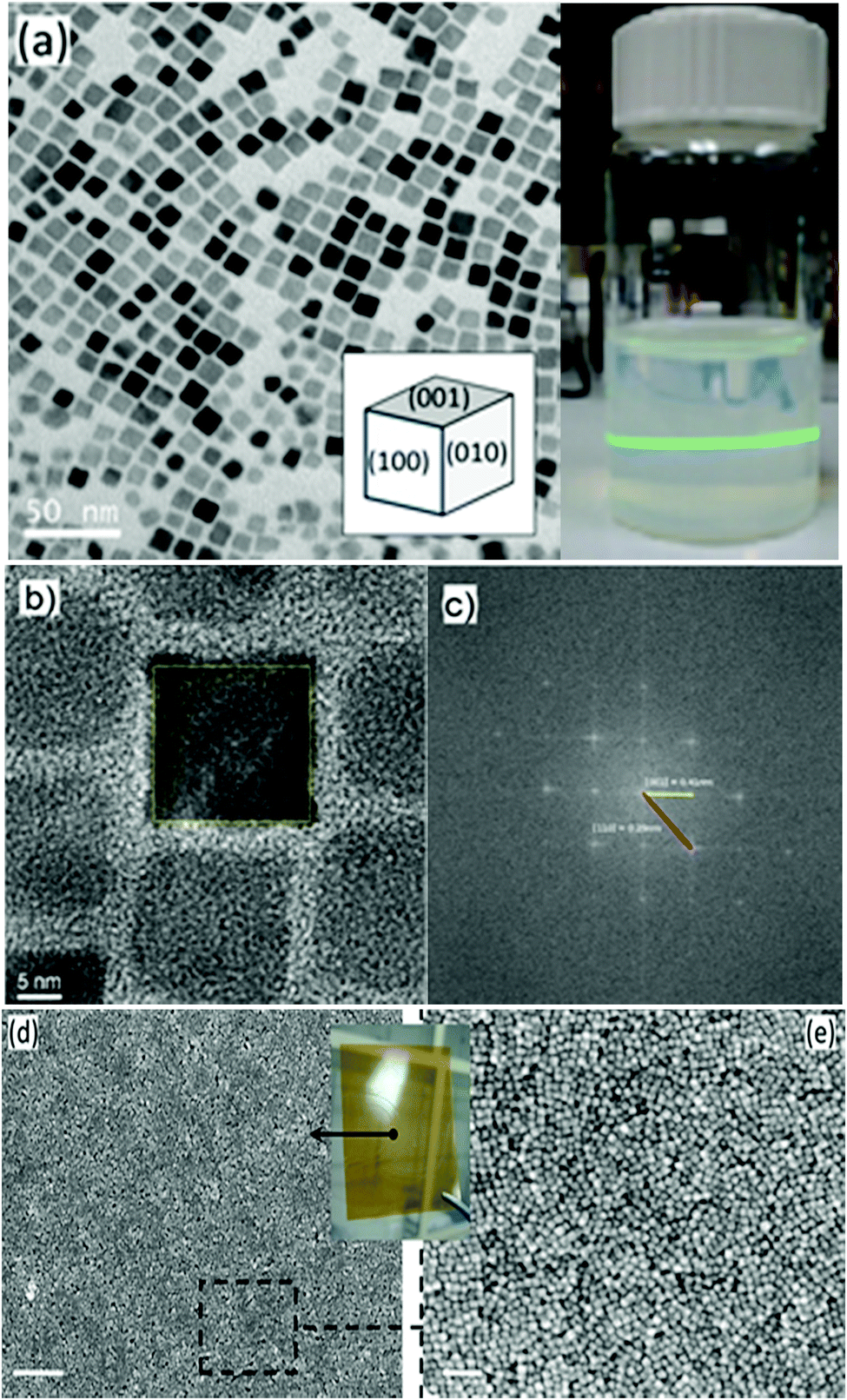
The transmission electron microscopy (TEM) micrograph (Fig. 1a) shows that the as-prepared BTO nanocrystals possess a regular cuboidal shape and have an average size of 15 nm. The high resolution TEM image of an individual BaTiO3 nanocube presented in Fig. 1b reveals that the nanocrystals are highly crystalline, despite the relatively low synthesis temperature and display well defined lattice fringes, with an interplanar distance d = 4.09 Å, corresponding to the (001) crystal planes, thereby confirming the high quality of the nanocrystals.6 The surface of BTO nanocubes is passivated with oleic acid (OA) molecules, which enable them to be dispersed in non-polar solvents with the formation of highly stable colloidal solutions (Fig. 1). As seen in Fig. 1, a laser beam passes through a toluene solution of 15 nm BaTO3 nanocubes without being scattered via the Tyndall effect, which suggests that the nanocrystals are well dispersed in solution and do not form aggregates to deflect the light. This observation confirms the high quality of the nanocrystals and their ability to be dispersed in nonpolar solvents with the formation of highly stable nanoparticle inks, which can be used for fabrication of dielectric films by various solution-based methods, including spin coating, dip coating, drop casting, spray-coating or inkjet printing. Moreover, when these colloidal solutions are processed on planar substrates followed by the controlled evaporation of the solvent, the nanocrystals form self-assembled monolayers and films, which can be densified by a post-deposition annealing process at 300 °C in air.
 |
| | Fig. 1 (a) Top view TEM image of 15 nm BTO NCs; (b) high resolution TEM image of an individual 15 nm BTO nanocube; (c) Fourier transform of the TEM image showing the reciprocal space; (d) and (e) Top view SEM image of BTO NCs thin films (scale bars, 500 nm and 100 nm, respectively) (inset: photograph of the BTO NCs film on a flexible substrate). | |
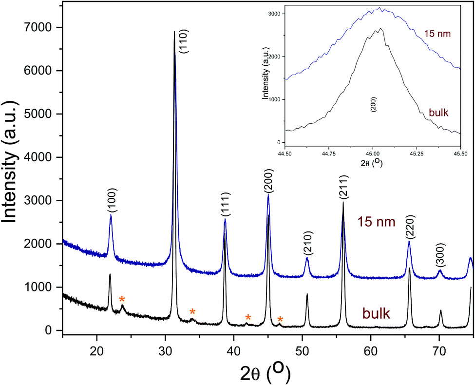
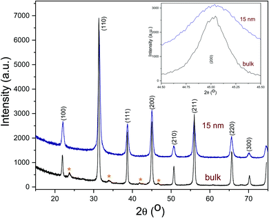
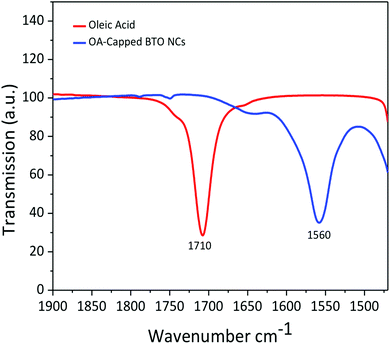
The composition and phase purity of the BaTiO3 nanocrystals was studied by conventional X-Ray powder diffraction. As seen in Fig. 2, the nanopowders containing 15 nm BaTiO3 nanocubes are well-crystallized and are free of impurities, such as BaCO3 which can be commonly observed in the pattern of commercial bulk BaTiO3 samples. It is worth mentioning that the analysis of the XRD patterns of nanoscale BaTiO3 is inconclusive with respect to revealing the presence of tetragonal distortion. This is because the splitting of the (200) peak around 45° in 2θ, commonly ascribed to the off-center shift of the Ti4+ ions within the TiO6 octahedra forming the perovskite structure is obscured by the peak broadening effect. Recent studies performed by our group using synchrotron X-ray diffraction and total scattering and Pair Distribution Function (PDF) techniques revealed that BaTiO3 nanocubes of different sizes possess an orthorhombic/tetragonal structure.35,36 As seen in Fig. 3, the presence of oleic acid molecules at the surface of BTO nanocubes was confirmed experimentally by the absorption bands at 1560 cm−1 in the Fourier-transform infrared (FTIR) spectra of the oleic acid capped BTO NCs, bands ascribed to the stretching modes of the carboxyl (C![[double bond, length as m-dash]](https://www.rsc.org/images/entities/char_e001.gif) O) moiety.
O) moiety.
 |
| | Fig. 2 Powder X-ray diffraction pattern of 15 nm BaTiO3 nanocubes compared to that of bulk BaTiO3. | |
 |
| | Fig. 3 Fourier-transform infrared (FTIR) spectra of the oleic acid capped BTO nanocubes. | |
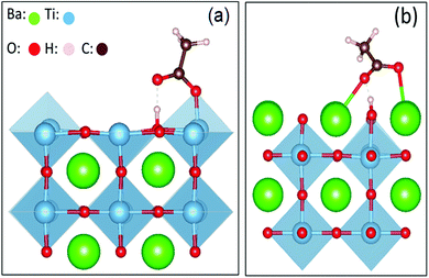
The microscopic interaction between the BaTiO3 nanocrystals and the capping agent molecules was simulated by calculating the binding energy of the carboxylic group bonded to the facets of the BaTiO3 nanocube.6 In this simulation, acetic acid was used as a simple model to study the binding energy of oleic acid absorbed on the surface of BTO, as the binding can mainly be ascribed to the interaction between the carboxylic molecule and the surface of the nanocrystal. The adsorption energy was calculated using the following formula:
| | | −Eads = −Eslab-molecule + (Eslab + Emolecule) | (1) |
where
Eslab-molecule is the total energy of the adsorption of the relaxed surface and the adsorbate molecule,
Eslab is the total energy of the relaxed slab, and
Emolecule is the energy of the relaxed isolated molecule. Schematic diagrams of the carboxylic molecule adsorbent on the surface of BTO crystal planes are shown in
Fig. 4a, and b, respectively.
 |
| | Fig. 4 Schematic diagrams of the carboxylic molecule adsorbent on the surface of BTO crystal planes. | |
The absorption energies were calculated using density functional theory (DFT), and the results are presented in Table 1. The results obtained from these calculations suggested that the absorption energy of acetic acid molecules in the TiO2-terminated {001} planes of BTO is higher than that of the BaO-terminated {001} BTO surface, thereby indicating that the bonding between the capping ligand molecules and TiO2 facet is favored. Based upon the previous results obtained by our group, we exploited here the uniformity in the shape and size of the as synthesized monodisperse BTO to design a highly versatile method to fabricate uniform and densely packed nanocrystal-based films to be used as gate dielectrics in the design of field effect transistors. To this end, thin film structures were fabricated by drop-casting colloidal solutions containing 15 nm BTO nanocubes on different substrates followed by the natural evaporation of the solvent. The morphology of the resulting films was studied by scanning electron microscopy (SEM) and top-view SEM images of representative BTO NC films deposited on 50 μm thick flexible polyimide (Kapton®) substrates and subsequently heat treated at 300 °C are presented in Fig. 5a–d. As shown in Fig. 5a, the films consist of a densely packed 15 nm BaTiO3 cuboidal which packs preferentially by sharing their faces. This alignment of the nanocubes is not perfect, which will lead to some spaces between the adjacent nanocubes; however the packing of the nanocubes is quite compact. To remove the oleic acid molecules and densify the films, the as-deposited films were subsequently annealed at 400 °C, this value of temperature being the maximum temperature tolerated by the Kapton substrates. The inspection of the SEM micrographs of the annealed films (Fig. 4a), reveals that heat treatment does not influence significantly the morphology and the multi-stacking structure of BTO NC films prepared at room temperature.
Table 1 Calculated absorption energies on the {001} planes of a BTO nanocube
| Surface index |
E
adsorption (eV) |
| BaO(001) |
3.78 |
| TiO2(001) |
4.01 |
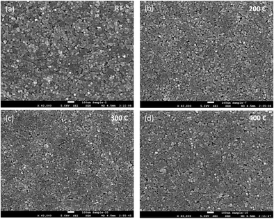 |
| | Fig. 5 Top view SEM images of BTO nanocube films after annealing at (a) room temperature (b) 200 °C, (c) 300 °C and (d) 400 °C. Scale bar represents 100 nm. | |
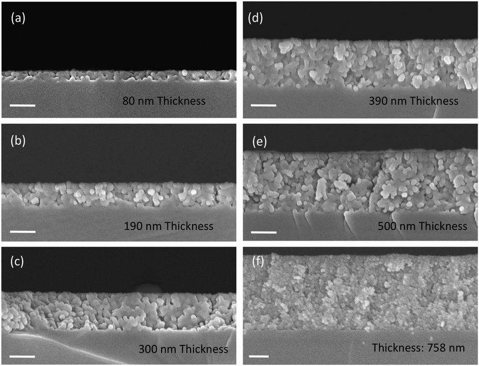
Fig. 6a–f show representative cross-section SEM images of thin films obtained by casting solutions containing 15 nm BaTiO3 nanocubes with different concentrations on a substrate and varying the number of deposited layers, respectively. The experimental results indicate that the film thickness increases linearly from 80 nm to 758 nm with the number of cast layers from 1 to 6, being dependent on both the number of cast layers and the concentration of BTO the colloidal solution. The films are constructed of small nanoparticles which are compact thereby forming dense films with a smooth surface. Also, as seen in Fig. 7, for the same number of layers cast on the substrate, the thickness of the films increases almost two times (from ∼140 nm to ∼290 nm for three layers or from ∼220 nm to ∼430 nm for five layers) when the concentration of the nanocrystals in solution was increased from 1.5 mg mL−1 to 7.5 mg mL−1. This observation clearly demonstrates that the thickness of the films can be controlled by varying either the number of cast layers and/or the concentration of the colloidal nanocrystals. The photograph image of BTO NCs film cast on a Kapton substrate (inset of Fig. 1) clearly demonstrates that the nanocrystal-based thin films present a high optical transparency along with increased mechanical flexibility, which makes them attractive candidates for the design of future unconventional electronics.
 |
| | Fig. 6 Cross section SEM images of nanoparticulate BaTiO3 thin films with different thicknesses. | |
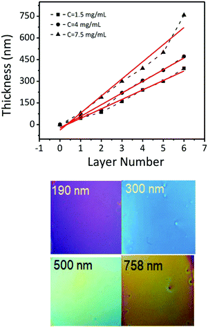 |
| | Fig. 7 Thickness dependence of the BTO nanocube thin films versus the number of layers and the concentration of solution. The color of the film changes from purple to magenta, green and orange when their thickness increases from 190, 300, 500 and 758 nm, respectively. | |
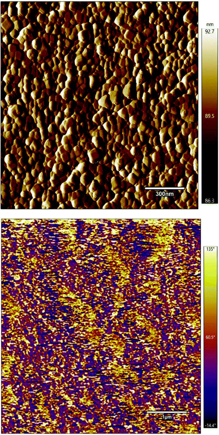
Self-assembled bilayer thin film structures based on BTO NCs as the dielectric layer and indium oxide (In2O3) QDs, as the semiconducting layer, were fabricated by a solution-based approach on a transparent and flexible substrate and subsequently incorporated into thin film transistors (FETs). Additionally, the surface morphology and roughness of the films were investigated by using atomic force microscopy. Fig. 8 shows a representative AFM image collected in tapping mode of the 300 nm thick BaTiO3 film. The image clearly shows that the film has a smooth and highly uniform surface, free of cracks or pinholes and consists of interconnected grains. The grain size of dielectric films plays an important role in their electrical properties since it is well known that small grains induce a low leakage current, thereby improving significantly the dielectric and ferroelectric response of these nanostructures.37,38 The roughness of the film was found to be 6.4 nm. These results are consistent with observations from SEM experiments, thereby indicating that the films deposited by this technique possess a smooth surface. The piezoresponse force microscopy (PFM) image (Fig. 8b) shows yellow and purple regions which correspond to the upward and downward orientation of the dielectric polarization, thereby indicating that the film is ferroelectric at room temperature.
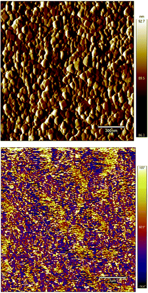 |
| | Fig. 8 AFM (a) and PFM (b) images of a 15 nm BTO nanocube film. | |
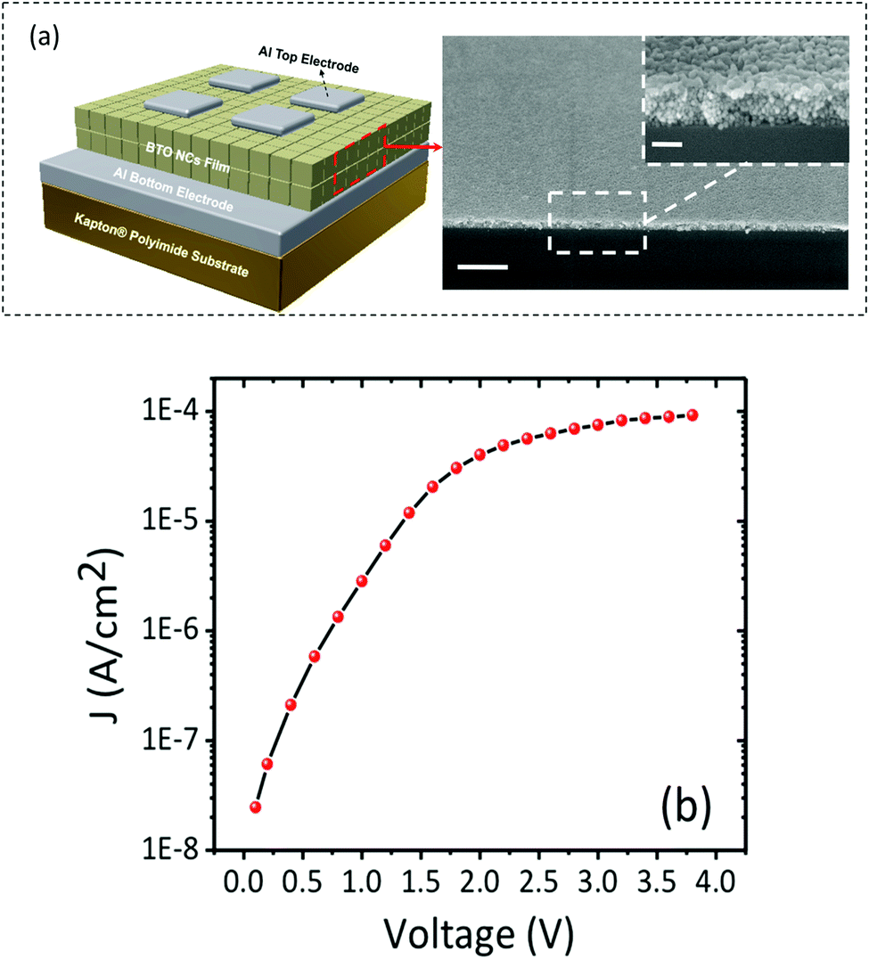
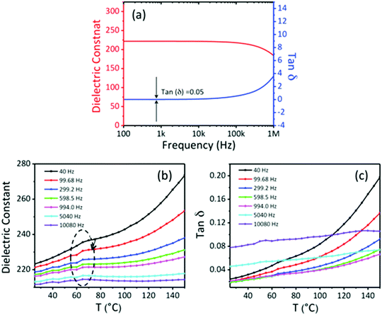
To investigate the dielectric properties of the self-assembled BTO NCs films obtained by drop-casting the ink suspension, two-terminal capacitors were fabricated in a parallel-plate geometry by using the thermal deposition of 75 nm-thick opaque aluminium electrodes on the 300 nm-thick BTO film. A schematic of the BTO capacitor and the cross-sectional SEM image of the BTO film from a tilted view are shown in Fig. 9a. Fig. 9b displays representative leakage current density–voltage (Jleak–V) curves of a BTO NCs-based capacitor. It is worth mentioning that the BTO capacitor presents a low leakage current density (∼8 × 10⁻⁵ A cm−2) after applying a bias voltage of 4 V, which strongly suggests that this value is the optimum in the range of operating voltages for these films. Fig. 10a exhibits the frequency variation of the dielectric permittivity (εr) and dielectric loss (tan![[thin space (1/6-em)]](https://www.rsc.org/images/entities/char_2009.gif) δ) for a capacitor containing a 500 nm thick BaTiO3 film measured in the range from 1 kHz to 1 MHz. At 1 kHz, the dielectric constant reaches a value εr =220, which is higher than those reported for BTO–polymer nanocomposites and bulk sintered pellets from BTO nanoparticles.24–26 The low value of the loss tangent (tanδ = 0.05) at 1 kHz, confirmed the existence of a limited direct ohmic and space charge conduction as the origin of dissipation in the BTO NCs thin films. One plausible reason for the increase of the value of the dielectric constant and loss with temperature in oxides is the existence of oxygen defects,39,40 whereas the enhancement of the dielectric loss in the high temperature region could be ascribed to either space charge polarization or the increase of the conductivity of the films with temperature.41 To better understand the mechanism underlying the variation of the dielectric constant and dielectric loss at high temperatures a systematic study of the dielectric behavior of BaTiO3 thin films with different thicknesses and the characterization of their oxygen defects using dielectric spectroscopy and XPS will be performed in the future and the results will be reported in a forthcoming paper.
δ) for a capacitor containing a 500 nm thick BaTiO3 film measured in the range from 1 kHz to 1 MHz. At 1 kHz, the dielectric constant reaches a value εr =220, which is higher than those reported for BTO–polymer nanocomposites and bulk sintered pellets from BTO nanoparticles.24–26 The low value of the loss tangent (tanδ = 0.05) at 1 kHz, confirmed the existence of a limited direct ohmic and space charge conduction as the origin of dissipation in the BTO NCs thin films. One plausible reason for the increase of the value of the dielectric constant and loss with temperature in oxides is the existence of oxygen defects,39,40 whereas the enhancement of the dielectric loss in the high temperature region could be ascribed to either space charge polarization or the increase of the conductivity of the films with temperature.41 To better understand the mechanism underlying the variation of the dielectric constant and dielectric loss at high temperatures a systematic study of the dielectric behavior of BaTiO3 thin films with different thicknesses and the characterization of their oxygen defects using dielectric spectroscopy and XPS will be performed in the future and the results will be reported in a forthcoming paper.
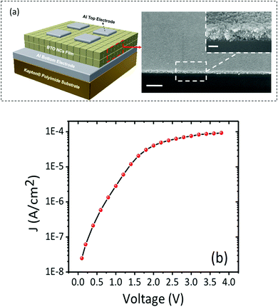 |
| | Fig. 9 (a) Schematic of a BTO NCs capacitor and cross-sectional SEM images of the BTO NCs film; (b) Jleak–V and (c) P–V characteristics of BTO NCs capacitors (scale bars, 200 nm and 1 μm, respectively). | |
 |
| | Fig. 10 Frequency (a) and temperature dependence of the dielectric constant (b) and loss tangent (c) of a 300 nm-thick BaTiO3 capacitor. | |
These experimental findings strongly suggest that the BTO films have excellent dielectric properties and are suitable candidates for integration into thin film transistors as dielectric gate layers. Fig. 10b shows the temperature dependent-dielectric constant at various frequencies. A small cusp can be observed around 65 °C for all frequencies in the dielectric constant spectra, its origin being currently investigated, and the results will be presented in a forthcoming paper. Using maps of ferroelectric structural distortions obtained from aberration-corrected TEM combined with holographic polarization imaging, we demonstrated previously that 15 nm cuboidal BaTiO3 colloidal nanocrystals possess an intrinsic, switchable polarization associated with an acentric structure and a ferroelectric order.42 In Fig. 11 are presented the results obtained by bit-mapped voltage lithography, which further confirms the existence of a polarization which can be reversibly switched with an external electric field. Upon applying a bias voltage of −20 V through the tip, all dielectric dipoles are oriented downwards with the external electric field which is greater than the local coercive field (orange area). Then, the tip is retracted, the bias voltage is reversed to a negative value (V = −20 V) and single domains in which the dipoles are reversed are written on the film (purple areas in Fig. 11a). Local PFM measurements of the poled regions (Fig. 11b) present well defined bipolar hysteresis loops as a function of the applied voltage. The 180° phase offset reveals the two antiparallel orientations of the polarization induced by different poling voltages. The coercive voltage is around 4 V, which can be reduced by decreasing the thickness of the BTO NCs film. This typical switching behavior indicates the possibility of using the self-assembled BTO NCs to operate as a nanoscale memory device, in which the direction of polarization is read out as logic “1” and “0” in binary code.
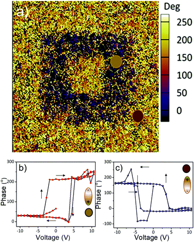 |
| | Fig. 11 (a) Out-of-plane phase contrast PFM image after writing an area of 3 μm2 with −20 V and then the inner 1 μm2 square with +20 V; PFM phase (b) and amplitude (c) plots. | |
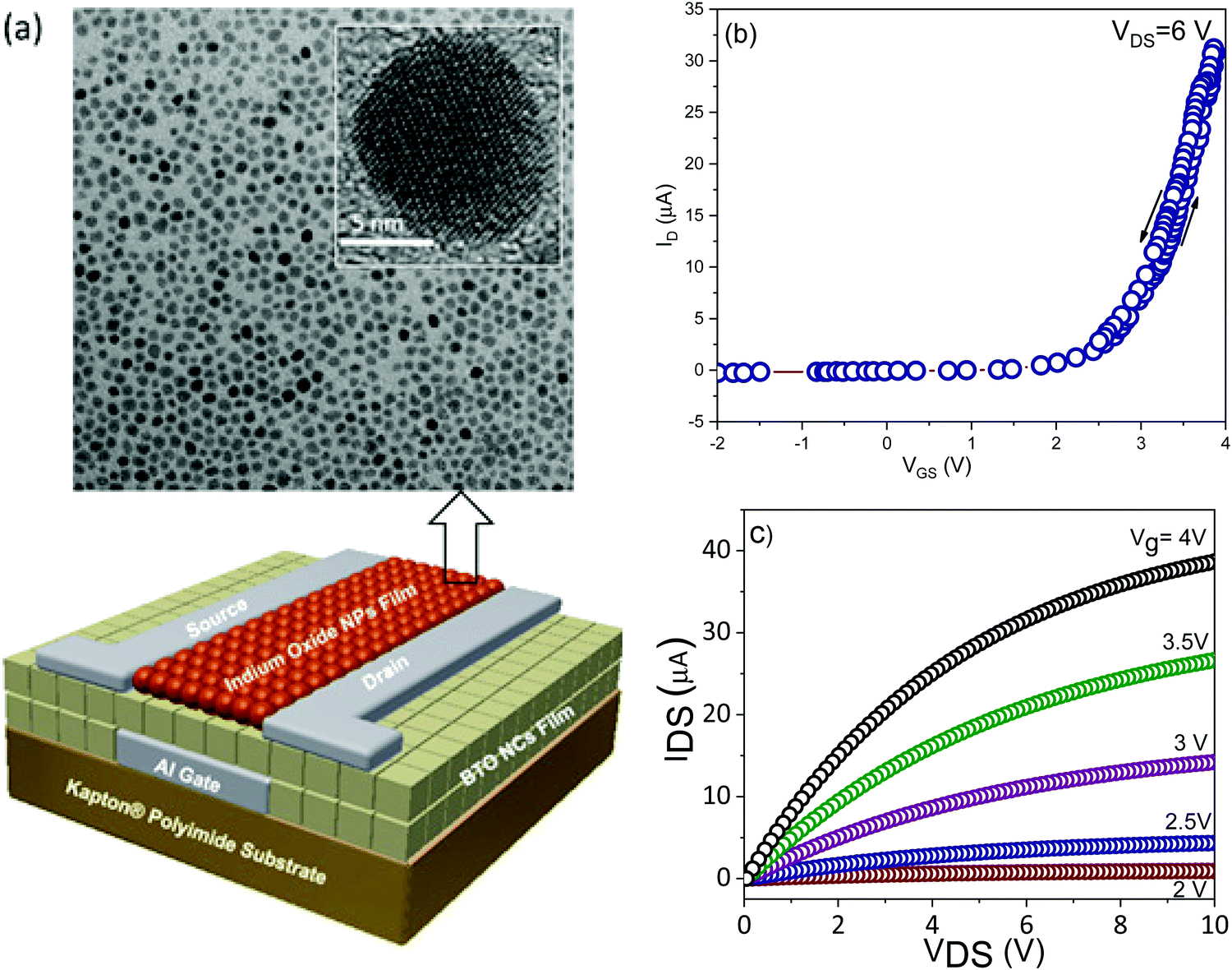
To demonstrate the potential of integration of ferroelectric nanocrystal-based thin films in flexible transistors, 15 nm BaTiO3 nanocubes were used as gate dielectrics into thin-film field effect transistors fabricated in a top-contact, bottom-gate configuration (Fig. 12a). The details of the nanofabrication of nanocrystal-based thin film transistors were described in the experimental section. The FET channel was fabricated by depositing a thin film made of spheroidal In2O3 colloidal nanocrystals on top of the ferroelectric gate film. The In2O3 nanocrystals used in this work were synthesized via a high temperature solution method, involving the thermolysis of metal–organic precursors at 300 °C.33 The as-synthesized nanocrystals are nearly monodisperse with an average size of 10 nm, as revealed by the TEM image (Fig. 12a). Top gate field effect thin film transistors were fabricated on Kapton substrates by patterning 75 nm-thick electrodes, including the bottom gate and top drain and source (width to channel length ratio, W/L, of 10) by using photolithography. Fig. 12b shows the transfer characteristics for the BaTiO3/In2O3 thin film transistor. As can be easily inferred, the transistor is characterized by a threshold voltage of 2.9 ± 0.05 V and possesses a very small hysteresis (0.1 ± 0.04 V). Moreover, the extracted values of the on/off ratio and subthreshold swing are Ion/Ioff ∼ 104 and SS = 808 mV decade−1. The subthreshold swing (SS) is the inverse of the subthreshold slope of the log drain current vs. the gate voltage (VG) below the threshold voltage (Vth), which defines the boundary between the subthreshold and transport regimes. Similarly, the carrier mobility was determined from the slope of the drain–source current (IDS) vs. the gate voltage (VG), as described by the equation:
| | 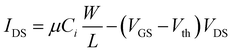 | (2) |
where
μ is the carrier mobility in the linear regime,
Ci is the capacitance of the dielectric gate,
W and
L are the width and length of the channel,
IDS is the drain–source current and
Vth and
VG are the threshold and gate voltages, respectively.
 |
| | Fig. 12 (a) Schematic of a solution-processed transistor using colloidal nanocrystals and a TEM image of the In2O3 quantum dots. Electrical performance of the BaTiO3/In2O3 flexible transistor: typical output (b) and transfer (c) characteristics of the flexible, transparent FET. | |
The calculated carrier mobility was μeff = 17.4 ± 0.2 cm2 V−1 s−1, a value which is higher than that reported in the literature for both inorganic and organic field effect transistors containing BaTiO3 nanoparticle films as the gate dielectric, which suggests that the BaTiO3 colloidal nanocrystals obtained by this synthetic method exhibit great potential for integration into flexible field effect transistors with superior performance characteristics.25,43Fig. 12c shows the output characteristics of the BTO–NCs-based FET, whereby the drain voltage and the gate bias were swept from 0 to 10 V and from 2 to 4 V, respectively. The experimental data confirmed the excellent n-type characteristics of the FET at low operating driving voltages. This is presumably facilitated by a low trapped state density, which will require the injection of a lower concentration of charge carriers. In turn, the trapped states at the dielectric/semiconductor interfaces are ascribed to the existence of surface defects, which can influence the charge transport by scattering and/or trapping the charges at the interfaces. A systematic study on the influence of the surface characteristics of BaTiO3 nanocubes on the trapped states is currently underway and will be presented in a future paper. It is worth noting that from the linear IDS–VDS relationship in the low bias region and the vanishing normalized contact resistances extracted using the transmission line method it was confirmed that Ohmic contacts are formed in these devices.
In summary, ferroelectric, nearly monodisperse 15 nm BaTiO3 cuboidal colloidal nanocrystals synthesized by a solvothermal technique were used to fabricate highly stable dielectric inks and high-k nanoparticle films as insulator layers which were tested in both a capacitor and transistor geometry. The passivation of the surface of the BaTiO3 nanocubes with oleic acid molecules, renders them dispersible in nonpolar solvents, thereby facilitating the fabrication of stable colloidal inks and the low temperature solution-phase processing and deposition of high capacitance, low leakage dielectric films on flexible substrates at low cost. We have shown in this work that ferroelectric surface passivated, monodisperse cuboidal nanocrystals can be successfully used for the design of ‘all inorganic’ flexible field effect transistors. Specifically, highly stable ink formulations containing 15 nm BaTiO3 nanocubes were used to fabricate dielectric layers used as the insulating gate in a FET interfaced with a semiconductor channel consisting of a dense film made by 10 nm monodisperse spheroidal In2O3 colloidal nanocrystals. The FET has shown output and transfer characteristics which are superior to those reported in the literature for other BaTiO3 NPs-based FETS, exhibiting a charge mobility of 17.4 ± 0.2 cm2 V−1 s−1 under 10 V and an on/off ratio of about 1 × 10⁴. This clearly demonstrates that the rigorous selection of inorganic colloidal nanocrystals with controlled morphology and surface composition and their assembly into thin film structures via solution processing is a viable method for the design of flexible FETs with superior performance characteristics. Combining the optimized dielectric gate with an In2O3 quantum dot semiconductor channel affords significant generality in the fabrication of solution-processed thin film transistors with Ion/Ioff ∼ 104 operating at voltages as low as ∼10 V.
Author contributions
D. C. synthesized and characterized the colloidal nanocrystals, G. C. and A. R. conceived the experiments, S. S. P. fabricated and characterized the devices and performed scanning probe microscopy and dielectric spectroscopy experiments, S.S. P.; G. C. and A. R. analyzed the results. All authors have approved the final version of the manuscript.
Conflicts of interest
There is no conflict of interests to declare.
Acknowledgements
This work was supported financially by the Office of Research and Graduate Studies at Central Michigan University (FRCE Grant No. 48401) and the Executive Agency for Higher Education, Research Development and Innovation Funding (Romania) through grant No. PN-III-P4-ID-PCCF2016-0175.
References
- Y. S. Rim, H. Chen, Y. Liu, S.-H. Bae, H. J. Kim and Y. Yang, ACS Nano, 2014, 8, 9680–9686 CrossRef CAS PubMed.
- Y.-G. Ha, K. Everaerts, M. C. Hersam and T. J. Marks, Acc. Chem. Res., 2014, 47, 1019–1028 CrossRef CAS PubMed.
- A. Zumeit, A. S. Dahiya, A. Christou, D. Shakthivel and R. Dahiya, npj Flexible Electron., 2021, 5, 18 CrossRef CAS.
- J. P. Rojas, G. A. Torres Sevilla, N. Alfaraj, M. T. Ghoneim, A. T. Kutbee, A. Sridharan and M. M. Hussain, ACS Nano, 2015, 9, 5255–5263 CrossRef CAS PubMed.
- M. Wang, Y. Luo, T. Wang, C. Wan, L. Pan, S. Pan, K. He, A. Neo and X. Chen, Adv. Mater., 2021, 33, 2003014 CrossRef CAS PubMed.
- V. V. Zyryanov, V. A. Sadykov, N. F. Uvarov, G. M. Alikina, A. I. Lukashevich, S. Neophytides and J. M. Criado, Solid State Ionics, 2005, 176, 2813–2818 CrossRef CAS.
- S. Salahuddin and S. Datta, Nano Lett., 2008, 8, 405–410 CrossRef CAS PubMed.
- J.-H. Choi, A. T. Fafarman, S. J. Oh, D.-K. Ko, D. K. Kim, B. T. Diroll, S. Muramoto, J. G. Gillen, C. B. Murray and C. R. Kagan, Nano Lett., 2012, 12, 2631–2638 CrossRef CAS PubMed.
- Q. Zhao, S. Yang, J. J. Ng, J. Xu, Y. C. Choi, C. B. Murray and C. R. Kagan, J. Phys. Chem. Lett., 2021, 12, 6514–6518 CrossRef CAS PubMed.
- D. C. Tripathi, L. Asor, G. Zaharoni, U. Banin and N. Tessler, J. Phys. Chem. C, 2019, 123, 18717–18725 CrossRef CAS.
- D. S. Dolzhnikov, H. Zhang, J. Jang, J. S. Son, M. G. Panthani, T. Shibata, S. Chattopadhyay and D. V. Talapin, Science, 2015, 347, 425–428 CrossRef CAS PubMed.
- J. Jang, D. S. Dolzhnikov, W. Liu, S. Nam, M. Shim and D. V. Talapin, Nano Lett., 2015, 15, 6309–6317 CrossRef CAS PubMed.
- S. Z. Bisri, C. Piliego, M. Yarema, W. Heiss and M. A. Loi, Adv. Mater., 2013, 25, 4309–4314 CrossRef CAS PubMed.
- W.-k Koh, S. R. Saudari, A. T. Fafarman, C. R. Kagan and C. B. Murray, Nano Lett., 2011, 11, 4764–4767 CrossRef CAS PubMed.
- M. V. Kovalenko, M. Scheele and D. V. Talapin, Science, 2009, 324, 1417 CrossRef CAS PubMed.
- T.-M. Pan, F.-H. Chen and Y.-H. Shao, RSC Adv., 2015, 5, 51286–51289 RSC.
- E. Fortunato, P. Barquinha and R. Martins, Adv. Mater., 2012, 24, 2945–2986 CrossRef CAS PubMed.
- H. Mulaosmanovic, E. T. Breyer, S. Dünkel, S. Beyer, T. Mikolajick and S. Slesazeck, Nanotechnology, 2021, 32, 502002 CrossRef CAS PubMed.
- T. Kim, J. Hwang, G. Kim, M. Jung and S. Jeon, Phys. Status Solidi RRL, 2021, 15, 2100018 CrossRef CAS.
- G. Niu, H.-D. Kim, R. Roelofs, E. Perez, M. A. Schubert, P. Zaumseil, I. Costina and C. Wenger, Sci. Rep., 2016, 6, 28155 CrossRef CAS PubMed.
- Y.-L. Wu, J.-J. Lin and C.-M. Ma, J. Phys. Chem. Solids, 2008, 69, 730–733 CrossRef CAS.
- Y. T. Jeong and A. Dodabalapur, Appl. Phys. Lett., 2007, 91, 193509 CrossRef.
- S. Ju, A. Facchetti, Y. Xuan, J. Liu, F. Ishikawa, P. Ye, C. Zhou, T. J. Marks and D. B. Janes, Nat. Nanotechnol., 2007, 2, 378–384 CrossRef CAS PubMed.
- J.-H. Choi, H. Wang, S. J. Oh, T. Paik, P. Sung, J. Sung, X. Ye, T. Zhao, B. T. Diroll, C. B. Murray and C. R. Kagan, Science, 2016, 352, 205 CrossRef CAS PubMed.
- H. T. Pham, J. H. Yang, D.-S. Lee, B. H. Lee and H.-D. Jeong, ACS Appl. Mater. Interfaces, 2016, 8, 7248–7256 CrossRef CAS PubMed.
- L. Huang, Z. Jia, I. Kymissis and S. O'Brien, Adv. Funct. Mater., 2010, 20, 554–560 CrossRef CAS.
- S. J. Oh, Z. Wang, N. E. Berry, J.-H. Choi, T. Zhao, E. A. Gaulding, T. Paik, Y. Lai, C. B. Murray and C. R. Kagan, Nano Lett., 2014, 14, 6210–6216 CrossRef CAS PubMed.
- D. K. Kim, Y. Lai, B. T. Diroll, C. B. Murray and C. R. Kagan, Nat. Commun., 2012, 3, 1216 CrossRef PubMed.
- H. Wang, D. J. Butler, D. B. Straus, N. Oh, F. Wu, J. Guo, K. Xue, J. D. Lee, C. B. Murray and C. R. Kagan, ACS Nano, 2019, 13, 2324–2333 CAS.
- J. W. Cho, S. J. Park, J. Kim, W. Kim, H. K. Park, Y. R. Do and B. K. Min, ACS Appl. Mater. Interfaces, 2012, 4, 849–853 CrossRef CAS PubMed.
- Y. H. Kim, K. Y. Kook, S. K. Hwang, C. M. Park and J. H. Cho, ACS Nano, 2014, 8, 2419 CrossRef CAS PubMed.
- B. Salonikidou, T. Yasunori, B. Le Borgne, J. England, T. Shizuo and R. A. Sporea, ACS Appl. Electron. Mater., 2019, 1, 2692–2700 CrossRef CAS.
- D. Caruntu, K. Yao, Z. Zhang, T. Austin, W. Zhou and C. J. O’Connor, J. Phys. Chem. C, 2010, 114, 4875–4886 CrossRef CAS.
- D. Caruntu, T. Rostamzadeh, T. Costanzo, S. Salemizadeh Parizi and G. Caruntu, Nanoscale, 2015, 7, 12955–12969 RSC.
- B. Jiang, C. Zhao, P. C. Metz, P. R. Jothi, B. Kavey, L. Reven, M. L. D'Addario, J. Jones, G. Caruntu and K. Page, J. Mater. Chem. C, 2022 10.1039/D2TC00477A.
- T. M. Usher, B. Kavey, G. Caruntu and K. Page, ACS Appl. Nano Mater., 2020, 3, 9715–9723 CrossRef CAS.
-
C. Sung-Dong, L. Joo-Yeon and P. Kyung-Wook, 2001.
-
J. Robertson and B. R. Varlow, 2004.
- G. Singh, V. S. Tiwari and P. K. Gupta, J. Appl. Phys., 2010, 107, 064103 CrossRef.
- K. Meng, W. Li, X. Tang, X. Guo, Q. Liu and Y. Jiang, Appl. Phys. A: Mater. Sci. Process., 2021, 127, 745 CrossRef CAS.
- T.-F. Zhang, X.-G. Tang, Q.-X. Liu, S.-G. Lu, Y.-P. Jiang, X.-X. Huang and Q.-F. Zhou, AIP Adv., 2014, 4, 107141 CrossRef.
- M. J. Polking, M.-G. Han, A. Yourdkhani, V. Petkov, C. F. Kisielowski, V. V. Volkov, Y. Zhu, G. Caruntu, A. Paul Alivisatos and R. Ramesh, Nat. Mater., 2012, 11, 700–709 CrossRef CAS PubMed.
- Q. J. Cai, Y. Gan, M. B. Chan-Park, H. B. Yang, Z. S. Lu, C. M. Li, J. Guo and Z. L. Dong, Chem. Mater., 2009, 21, 3153–3161 CrossRef CAS.
|
| This journal is © The Royal Society of Chemistry 2022 |
Click here to see how this site uses Cookies. View our privacy policy here. 
 Open Access Article
 This Open Access Article is licensed under a Creative Commons Attribution-Non Commercial 3.0 Unported Licence
 *abc
*abc