
 Open Access Article
 This Open Access Article is licensed under a Creative Commons Attribution-Non Commercial 3.0 Unported Licence
Progress in the preparation and application of CsPbX3 perovskites
Yingwen
Pan
 ab,
Yaofang
Zhang
*ab,
Weimin
Kang
ac,
Nanping
Deng
ac,
Zirui
Yan
ab,
Wei
Sun
ab,
Xiaoying
Kang
ab and
Jian
Ni
d
ab,
Yaofang
Zhang
*ab,
Weimin
Kang
ac,
Nanping
Deng
ac,
Zirui
Yan
ab,
Wei
Sun
ab,
Xiaoying
Kang
ab and
Jian
Ni
d
aState Key Laboratory of Separation Membranes and Membrane Processes, Tiangong University, Tianjin 300387, P. R. China. E-mail: zhangyaofang@tiangong.edu.cn
bSchool of Physical Science and Technology, Tiangong University, Tianjin 300387, P. R. China
cSchool of Textile Science and Engineering, Tiangong University, Tianjin 300387, P. R. China
dDepartment of Electronic Science and Technology, College of Electronic Information and Optical Engineering, Nankai University, Tianjin, 300350, China
First published on 12th April 2022
Abstract
In recent years, organic–inorganic metal halide (OIH) perovskites have become a popular material of increasing interest. Due to the presence of organic cations, OIH perovskites suffer from chemical instability and easy decomposition in harsh environments with high temperature and humidity. All-inorganic perovskites have better stability compared to OIH perovskites. Due to the intensive research and continuous optimization of the preparation process, the power conversion efficiency (PCE) of all-inorganic perovskite solar cells (PSCs) has exceeded 20%. Therefore, all-inorganic CsPbX3 (X = Br, I, CI) perovskites are becoming popular and are potential materials suitable for optoelectronic devices. CsPbX3 perovskites exhibit many excellent physical and optical properties, such as high carrier mobility and high fluorescence. In this review, recent progress on the preparation and application of CsPbX3 perovskites is outlined. Firstly, the physical structure and excellent optical properties of CsPbX3 perovskites are briefly described. Next, the preparation of different morphologies of CsPbX3 perovskites is described. Furthermore, this paper summarizes the application of CsPbX3 in optoelectronic devices, including PSCs, light-emitting diodes (LEDs), and photodetectors (PDs). The performance parameters of CsPbX3 devices are summarized. Finally, a brief summary of the full paper is presented and the challenges facing the field of all-inorganic CsPbX3 perovskites are discussed.
1. Introduction
OIH perovskites are popular and promising materials that have aroused tremendous public attention due to their excellent photoelectric properties, such as high absorptivity, high carrier mobility, smaller exciton binding energy, and adjustable bandgap.9–13 Perovskites were originally discovered by a German mineralogist Gustav Rose in 1839; the first discovered perovskite-structure substance was CaTiO3.14,15 OIH perovskites possess the general molecular formula ABX3, which is composed of three ions occupying different positions of the crystal lattice. The A site is a monovalent organic cation that has a larger ionic radius, where A = methylammonium (CH3NH3+, MA+) or formamidinium (CH3(NH2)2+, FA+).22 The B site is a metal cation whose ionic radius is smaller than that of A, where B = Pb2+, Sn2+ or Ge2+.24 The X site is a halide anion, where X = Cl−, Br− or I−. Fig. 1a shows the crystal structure of the perovskite CaTiO3 and Fig. 1b shows the crystal structure of OIH perovskites. The A ion occupies the octahedral void and is located in the centre of the cubic cell. The B metal cations are located at the apex of the cubic cell and are surrounded by six halogen anions. Thus, the perovskite has excellent photoelectric properties because of its unique physical structure.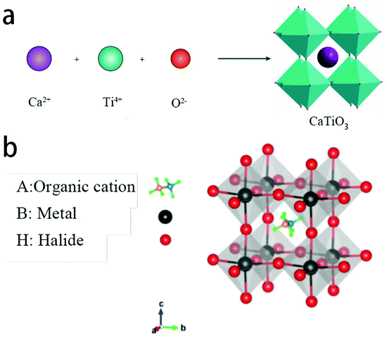 | ||
| Fig. 1 (a) The crystal structure of the perovskite CaTiO3.34 Copyright 2017, Springer Nature. (b) The crystal structure of OIH perovskites.36 Copyright 2020, Walter de Gruyter. | ||
Although OIH perovskites have many outstanding properties, their stability issues greatly limit their application. For instance, they are very sensitive to harsh environments. Due to the instability of organic cations in OIH perovskites, they decompose easily at high humidity and temperature.19,24 Xue et al. studied the structural properties during the decomposition of MAPbI3 (MA = CH3NH3+) by first-principles calculations.30 The intrinsically poor structural stability of MAPbI3 can cause it to decompose into PbI2, whether in high humidity or not. In addition, high temperature will cause the perovskite phase transition, which results in instability of the perovskite. For instance, the black perovskite-type (α-phase) of FAPbI3 is stable at high temperatures above 160 °C, but it turns into the yellow δ-phase when exposed to low temperatures and moisture.40 Moreover, Schwenzer et al. investigated the effects of different cation compositions on the thermal stability of perovskite thin films; the surface material composition of FACsPbI3 films was less affected than that of FAPbI3 films after 500 h at 85 °C.41 The poor thermal and moisture stability of organic–inorganic hybrid perovskite materials is caused by the facile phase transitions and the formation of hydrated phases near room temperature.43 Kulbak et al. explored the thermal stability of MAPbBr3 and CsPbBr3 by thermogravimetric analysis.44 MAPbBr3 began to decompose at 220 °C, while CsPbBr3 began to decompose at 580 °C; this indicates that all-inorganic perovskites have higher thermal stability than OIH perovskites. Therefore, it is known that all-inorganic perovskites are more stable than OIH perovskites.45 All-inorganic perovskite nanocrystals (PNCs) have advantages of high photoluminescence quantum yield (PLQY), narrow band emission, and adjustable fluorescence wavelength.46
In recent years, increasing numbers of scholars have focused on all-inorganic perovskite materials owing to their unique advantages. The A site in the perovskite general formula can be replaced by an inorganic cation. In a perovskite structure, its structure and stability are determined by the tolerance factor t and octahedral factor μ.47 In DFT calculations at 0 K, the γ phase is always the most stable, and the most ideal perovskite structure is the α phase, which has a tolerance factor of t = 1; however, it is unstable.48 When 0.81 < t < 1.11 and 0.44 < μ < 0.90, the crystal structure of perovskite is stable.11 When t < 0.89, perovskite is a tetragonal (β-phase) or orthogonal (γ-phase) structure with poor symmetry. The Cs+ ion can match the requirements of t, and it has replaced organic cations to improve the stability of perovskite in applications.
According to the citation report of American Chemical Society (ACS) Publications, we can conclude that the publications of CsPbX3 have shown an upward trend in the last 10 years. Moreover, the hot injection method was the first to emerge, and in recent years, the new electrospinning method has gradually arisen (Fig. 2). In addition, based on the hot injection method, the PCE of CsPbX3-based PSCs has improved from 5.8% (CsPbBr3) and 2.9% (CsPbI3) to 17.1% (CsPbI3) from the first paper in 2015 to date, and the stability has been continuously improved.49 Tong et al. improved the hot injection method, such as adding zeolite-encapsulated CsPbX3 NCs, doping with Mn+, and in situ growth of CsPbX3 NCs in metal-organic framework crystals, which improved the luminescence efficiency of the materials.7,17,28,50–57 Zhang et al. prepared dense and uniform CsPbX3 thin films by thermal evaporation and applied them in lasers, LEDs, PSCs, and other photoelectric fields.1,16,35,58–64 In recent years, electrospinning has emerged as a new method to prepare CsPbX3. Huang et al. encapsulated CsPbX3 NCs in different polymers and prepared CsPbX3 nanofibers by electrospinning.5,19,46,65–70
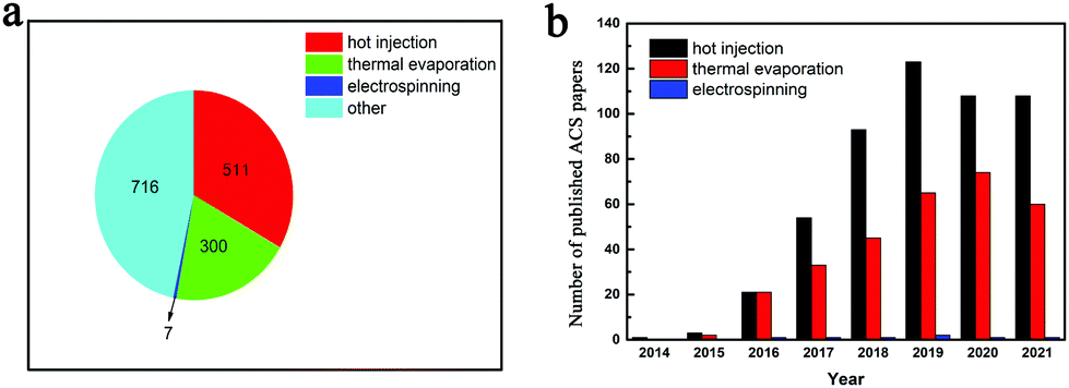 | ||
| Fig. 2 (a) Number of articles on the three preparation methods of CsPbX3 as percentages of core publications. (b) Statistics of core publications based on CsPbX3 preparation methods. | ||
Here, in this review, we will describe the latest progress of CsPbX3 perovskites and their applications in optoelectronic devices. The synthesis of CsPbX3 perovskites in different morphologies, including single crystals, thin films and nanocrystals, are first described. Then, the optoelectronic applications of CsPbX3 perovskite are reviewed, including PSCs, LEDs, and PDs. Finally, the challenges and prospects of the CsPbX3 perovskites are discussed.
2. Synthesis of CsPbX3 perovskites
To explore the characteristics of CsPbX3 perovskites and the application of different optoelectronic devices, various synthesis strategies of CsPbX3 perovskites in different morphologies were summarized, such as single crystals, thin films and nanocrystals.2.1 Synthesis of single crystals
Single crystals of all-inorganic perovskites are typically prepared by the Bridgman growth method. Song et al. obtained ultralarge 25 cm3-volume CsPbBr3 SC ingot through an improved Bridgman growth method using a four-zone furnace.6 The CsPbBr3 SC was prepared by the reaction of equimolar amounts of CsBr (42.6 g) and PbBr2 (73.4 g) in fused silica ampoules. A schematic of the growth is shown in Fig. 3a.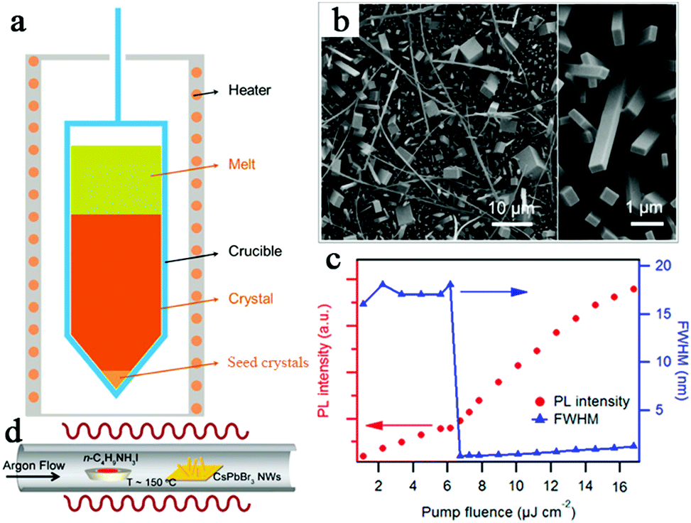 | ||
| Fig. 3 (a) Schematic diagram of the growth of a crystal by the Bridgeman method.6 Copyright 2017, John Wiley and Sons Inc. (b) Scanning electron microscope (SEM) image of the CsPbBr3 nanostructure. The inset on the right is a magnified SEM image.18 (c) Integrated emission intensity and full width at half maximum (FWHM) of the dominant emission peak plotted as a function of P, which shows that the lasing threshold is 6.2 μJ cm−2.18 (d) Schematic diagram of the vapour conversion of CsPbBr3 nanostructures into CsPb(Br,I)3.18 Copyright 2016, American Chemical Society. | ||
In addition to the traditional Bridgman growth method, the solution growth method has been developed to obtain high-quality perovskite single crystals. Fu et al. prepared solution-grown CsPbBr3, CsPbCl3 and their halide alloys of CsPb(Br,Cl)3 with high-quality single crystal nanostructures.18 Nanoplates and nanocrystals were prepared by reacting PbX2 and lead acetate films with CsBr (CsCl) solutions with methanol at room temperature. Fig. 3b displays the SEM image of CsPbBr3 NWs grown at room temperature for approximately 15 hours. As shown in Fig. 3c, the photoluminescence (PL) spectrum of CsPbBr3 NW peaked at 530 nm, with a FWHM of 17 nm. Since the direct synthesis of CsPb(Br,I)3 NWs by the solution method is challenging, the low temperature vapor-phase method was developed. As shown in Fig. 3d, CsPbBr3 NWs were successfully converted to CsPbI3 by a low temperature vapor-phase halide exchange process, maintaining the NW morphology and perovskite lattice.
2.2 Preparation of thin films
Typically, perovskite films can be prepared by the solution method or by thermal evaporation. The thin films prepared by traditional thermal evaporation are compact, uniform and reproducible, and this method can be used to prepare large-area uniform perovskite thin films.1,60 Thermal evaporation mainly refers to vapor deposition; H. J. Snaith's group at the University of Oxford prepared planar heterojunction perovskite solar cells with 15% PCE using the vapor deposition method for the first time.1Fig. 4a illustrates the process of the preparation of CH3NH3PbI3-xClx thin films by dual-source vapor deposition, in which organic source methylammonium iodide and inorganic source PbI2 were used for dual-source thermal evaporation.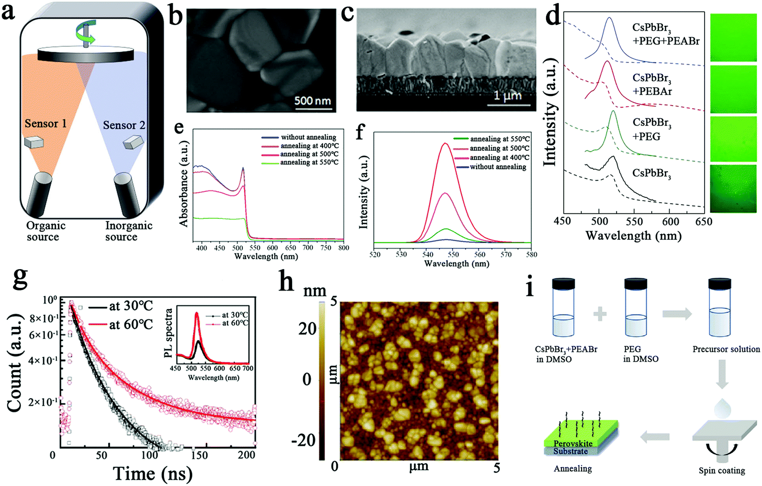 | ||
| Fig. 4 (a) Schematic diagram of the dual-source thermal evaporation system: the organic source is methylammonium iodide and the inorganic source is PbI2.1 Copyright 2013, Springer Nature. (b) Surface SEM images of deposited CsPbBr3 films under annealing at 500 °C.16 (c) Cross-sectional SEM images of deposited CsPbBr3 films under annealing at 500 °C.16 (d) Absorption (dashed line) and PL (solid line) spectra of CsPbBr3 films on a quartz substrate.26 (e) UV-Vis absorption spectra of deposited CsPbBr3 films under different annealing temperatures.16 (f) PL spectra of deposited CsPbBr3 films under different annealing temperatures.16 Copyright 2018, Elsevier BV. (g) Time-resolved photoluminescence (TRPL) and steady-state photoluminescence spectroscopy (inset).35 (h) AFM images of 100 nm thick CsPbBr3 films prepared at 60 °C with deposition rates of 1.0 Å s−1.35 Copyright 2020, American Chemical Society. (i) Preparation process of CsPbBr3 perovskite thin films.26 Copyright 2019, John Wiley and Sons Inc. | ||
Liu et al. prepared CsPbBr3 perovskite films by dual-source co-evaporation of CsBr and PbBr2 under vacuum conditions.16 When the substrate temperature was 300 °C and the evaporation rate ratio was 0.7![[thin space (1/6-em)]](https://www.rsc.org/images/entities/char_2009.gif) :1, the best crystallinity and optimum stoichiometry of the CsPbBr3 films were displayed. In addition, the CsPbBr3 film films annealed at 500 °C had the largest grains, and they were tightly connected, as shown in Fig. 4b and c. This shows that photocarriers can travel to opposite electrodes without crossing through grain boundaries, which yields excellent photovoltaic performance. Fig. 4e and f shows the UV-Vis absorbance spectra of the deposited CsPbBr3 films under different annealing temperatures, and the PL peak of all the films was 520 nm. On this basis, stable planar CsPbBr3 solar cells were prepared with an efficiency of up to 6.95%. This finding suggests that dual-source thermal co-evaporation is an effective method for preparing CsPbBr3 films with excellent properties.
:1, the best crystallinity and optimum stoichiometry of the CsPbBr3 films were displayed. In addition, the CsPbBr3 film films annealed at 500 °C had the largest grains, and they were tightly connected, as shown in Fig. 4b and c. This shows that photocarriers can travel to opposite electrodes without crossing through grain boundaries, which yields excellent photovoltaic performance. Fig. 4e and f shows the UV-Vis absorbance spectra of the deposited CsPbBr3 films under different annealing temperatures, and the PL peak of all the films was 520 nm. On this basis, stable planar CsPbBr3 solar cells were prepared with an efficiency of up to 6.95%. This finding suggests that dual-source thermal co-evaporation is an effective method for preparing CsPbBr3 films with excellent properties.
Yang et al. prepared CsPbBr3 perovskite films by thermal co-evaporation combined with continuous low-temperature thermal annealing and studied their morphology and crystallization processes.35 Dense and uniform CsPbBr3 grains with an average size of 150 ± 74 nm were formed at a standard deposition rate of 1.0 Å s−1 at 60 °C. As shown in the inset of Fig. 4g, the steady-state photoluminescence spectra of CsPbBr3 perovskite films prepared at 60 °C is superior to that of films prepared at 30 °C. When the deposition rate is 1.0 Å s−1, a CsPbBr3 film with a smoother surface can be seen under atomic force microscopy (AFM) in Fig. 4h. This article revealed for the first time the regulation of grain size and densification of CsPbBr3 films during thermal co-evaporation fabrication by in situ thermal dynamic crystallization.
The general solution method for the preparation of perovskite films is a one-step or two-step spin coating method. Due to the morphological defects and serious non-radiative recombination of all-inorganic perovskite, the efficiency of the device is seriously affected. Tang et al. doped two additives, PEABr and polyethylene glycol (PEG), to prepare CsPbBr3 perovskite films using the spin-coating method to passivate defects at the grain boundaries and thus reduce non-radiative recombination.26Fig. 4i shows the preparation process of the CsPbBr3 perovskite films with the PEG and PEABr additives. Fig. 4d shows the PL spectra of various CsPbBr3 perovskite films on PEDOT:PSS peaking at 520 nm. This method provides an effective strategy for preparing perovskite thin films with high density and few defects.
2.3 Synthesis of nanocrystals
All-inorganic perovskite nanocrystals can be synthesised by a variety of methods, the most mainstream being hot injection. The hot injection method has been widely used in the synthesis of traditional metal chalcogenide (PbS, CdS, CdSe) nanocrystals, and it is currently widely used for the preparation of quantum dots.71 Based on the traditional quantum dot synthesis method, efficient luminescent CsPbX3 nanocrystals (NCs) were synthesized by hot injection.72 In the hot injection method, the precursor solution was injected rapidly into the remaining solution of the synthetic compound under an inert atmosphere and a certain temperature, as can be seen in Fig. 5a.2,73 For the synthesis of CsPbX3 NCs, the Cs-containing precursor was first injected rapidly into the PbX2 precursor solution containing the organic ligand at a certain temperature.74 The precursor solution reacted in a high boiling point solvent with ligand-controlled growth to induce nucleation and obtain uniformly sized CsPbX3 nanocrystals.In 2015, Kovalenko et al. first prepared CsPbX3 (X = Cl, Br, I and halogen mixtures) perovskite nanocrystals using the hot injection method.17 They prepared CsPbX3 NCs that possess 4–15 nm cubic perovskite crystals. Fig. 5b shows transmission electron microscopy (TEM) images of the CsPbBr3 NCs; the size of the grains is uniformly distributed around 8 nm. As shown in Fig. 5c, the emission spectrum of the CsPbX3 NCs is tunable in the entire visible spectral region of 410–700 nm by varying the ratio of the halides, and the corresponding FWHMs can be measured as 12–42 nm. CsPbX3 NCs have high quantum yields of 50–90% and short radiation lifetimes of 1–29 ns, as can be seen in Fig. 5d. Fig. 5e shows the absorption and emission spectra of CsPbX3.
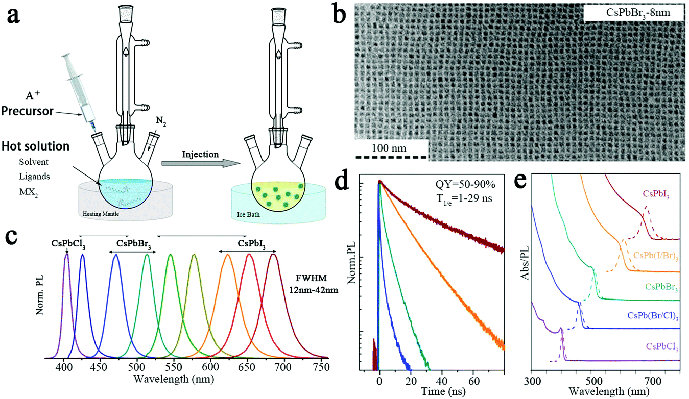 | ||
| Fig. 5 (a) Schematic diagram of the hot injection method.2 Copyright 2019, American Chemical Society. (b) TEM images of the CsPbBr3 NCs.17 (c) PL spectrum of the CsPbX3 NCs.17 (d) Time-resolved PL decay for all samples shown in (c) except CsPbCl3.17 (e) Typical optical absorption and PL spectra.17 Copyright 2015, American Chemical Society. | ||
In recent years, CsPbX3 perovskite quantum dots (PeQDs) have been embedded in intermediate structure metal–organic framework crystals (MOFs) to improve the stability of the PeQDs. In 2018, Wang's group prepared green-emitting CsPbBr3 and red-emitting CsPbBr0.6I2.4 PeQDs by hot injection and embedded CsPbX3 PeQDs into intermediate structured zinc-based metal organic-framework (MOF-5) crystals to improve the stability of the PeQDs.7 The PLQYs of the CsPbBr3/MOF-5 and CsPbBr0.6I2.4/MOF-5 composites were 52% and 56%, respectively; these were much higher than the PLQY of pure CsPbX3 powder, indicating that MOF-5 improved the performance of the CsPbX3 PeQDs. The average composite lifetimes of the CsPbBr3/MOF-5 and CsPbBr0.6I2.4/MOF-5 composites were longer than those of the pure CsPbX3 PeQDs (Fig. 6a). CsPbBr3/MOF-5 maintained 72.8% of its initial PL intensity at 80 °C and could also emit light at 120 °C, which demonstrated the high thermal stability of CsPbBr3/MOF-5 (Fig. 6b). CsPbBr3/MOF-5 maintained 79.2% photoluminescence intensity after 60 days at room temperature, which demonstrated its good long-term storage stability (Fig. 6c). In addition, Zhao et al. grew CsPbX3 (X = Cl, Br, and I) QDs in situ in zeolitic imidazolate framework-8 (ZIF-8), which improved the stability of the CsPbX3 QDs.25 The synthesis process of CsPbX3/ZIF-8 is shown in Fig. 6d. Furthermore, ZIF-8 can control the size of CsPbX3 quantum dots. Among them, the PLQY of CsPbBr3/ZIF-8 is up to 72%.
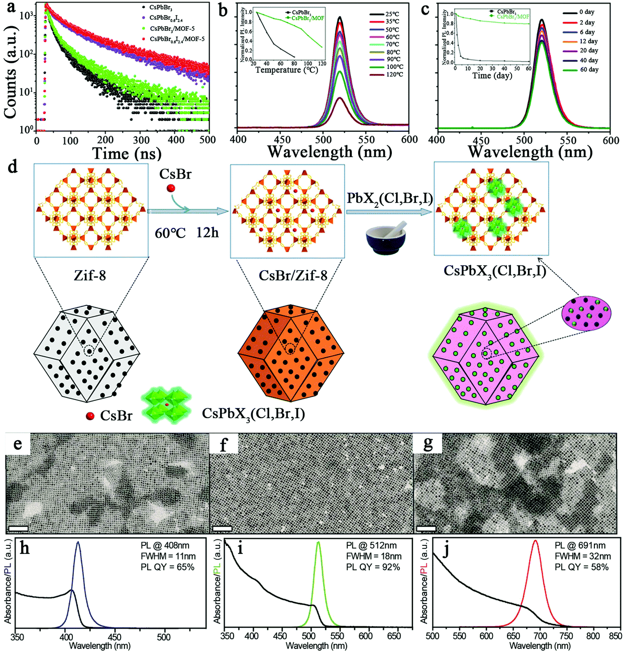 | ||
| Fig. 6 (a) Time-resolved photoluminescence decay curves of the CsPbBr3 powder, CsPbBr0.6I2.4,CsPbBr3/MOF-5 and CsPbBr0.6I2.4/MOF-5 composites.7 (b) Thermal stability test.7 (c) Long-term storage stability test of CsPbBr3/MOF-5.7 Copyright 2019, Elsevier. (d) Synthesis of CsPbX3/ZIF-8.25 Copyright 2021, American Chemical Society. TEM images of (e) CsPbCl3, (f) CsPbBr3, and (g) CsPbI3 NCs. Absorption and PL spectra of (h) CsPbCl3, (i) CsPbBr3, and (j) CsPbI3 NCs dispersed in toluene.28 Copyright 2018, American Chemical Society. | ||
Imran et al. replaced the halide precursor PbX2 (X = Cl, Br or I) salt with benzoyl halide in the hot injection method, which facilitates the injection of the metal cation and the desired ligands into the solution.28 This method also allows strict control of the size distribution, regulation of the CsPbX3 NC components and high phase purity. Fig. 6e–g shows TEM images of CsPbX3. Fig. 6h–j shows the emission peaks of the PL spectra of CsPbX3 NCs and the narrow FWHMs of the CsPbX3 NCs, from 11 nm (X = Cl) to 18 nm (X = Br) to 32 nm (X = I). In addition, the PLQYs of the CsPbBr3 NCs were up to 92%. The synthesized CsPbX3 NCs showed high phase stability, uniform size distribution, and unprecedented optical properties.
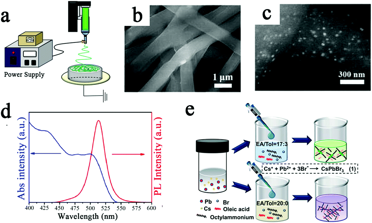
Electrospinning has become a popular method for the preparation of nanofibers in recent years, and it has aroused public attention because of its low cost, easy fabrication process, and fine-tuning of the morphology of fibers, as well as the large specific surface area of the prepared fibers.5,75 Electrospinning technology is used to prepare nanofibers by overcoming the surface tension of the jet and the internal viscous force by using electrostatic forces as the traction force.76 A schematic of the electrospinning process is shown in Fig. 7a. The CsPbBr3 NCs were coated with polymer by electrospinning, which improved their water and heat resistance, showing their promising application in optoelectronic devices.
 | ||
| Fig. 7 (a) Schematic diagram of the CsPbX3 (X = Cl, Br, I) nanofiber preparation process.5 Copyright 2019, American Institute of Physics. (b) SEM images of the CsPbBr3@PS fibers.19 (c) Typical backscattered electron SEM images of the CsPbBr3@PS fibers.19 (d) UV-vis absorption and PL spectra of the CsPbBr3@PS fibers.19 Copyright 2018, John Wiley and Sons Inc. (e) Schematic diagram of the process for synthesising CsPbBr3 nanorods and nanowires.29 Copyright 2021, Royal Society of Chemistry. | ||
Liao et al. investigated a general strategy that is based on the one-step electrospinning method to grow CsPbX3 NC in situ in fibers.19 The composition of CsPbX3 can be finely tuned to be uniformly encapsulated in polymer (PS) fibers by reasonably adjusting the ratio of PbX2 and CsX salts in the precursor solution. Fig. 7b displays a typical SEM image of the CsPbBr3@PS fiber film with 300 mg mL−1 PS; the average diameter of the fibers is 800 nm. The average size of CsPbBr3 NCs encapsulated in fibers is about 20 nm (Fig. 7c). Fig. 7d shows a clear absorption peak at around 500 nm and a PL emission peak at 513 nm with an FWHM of 24 nm. The PLQY values of CsPbBr3@PS remained above 70% of their original values after immersion in water for 192 h and above 50% after heating at 80 °C for 120 min. Eventually, the CsPbBr3@polymer fibers prepared by this method showed greatly improved water thermal stability and a PLQY of 48%.
Ligand-assisted reprecipitation (LARP) is also a facile method for the synthesis of CsPbX3 NCs at room temperature. Lai et al. applied the green solvent acetic acid instead of DMF to the LARP technique for the controlled synthesis of CsPbBr3 NCs under ambient conditions.29 The workflow of LARP technology is shown in Fig. 7e. The length of the CsPbBr3 NCs can be varied by changing the EA/Tol volume ratio to adjust the polarity of the antisolvent medium, enabling continuous conversion from nanorods to NWs. The prepared CsPbBr3 NCs have broad photoluminescence (471–508 nm) and a high quantum yield of up to 78%.
To clearly summarize the preparation processes and optical properties of different CsPbX3 materials, the recent developments of the different preparation methods and different compositions of CsPbX3 are detailed in Table 1.
| Materials | Shapes | Preparation methods | PL peaks (nm) | PLQY | FWHMs (nm) | Ref. |
|---|---|---|---|---|---|---|
| CsPbBr3 | Single crystal | Solution growth | 530 | — | 17 | 18 |
| CsPbBr3 | Single crystal | Bridgman growth | 527–538 | — | — | 6 |
| CsPbBr3 | Film | solution process | 520 | — | — | 26 |
| CsPbBr3 | Film | Thermal evaporation | 522.5 | 15.7% | 18.5 | 58 |
| CsPbBr3 | Film | Thermal evaporation | 525 | 12.2% | 18 | 59 |
| CsPbBr3 | Film | Thermal evaporation | 547 | — | — | 16 |
| CsPbBr3 | Film | Thermal evaporation | 524 | 7.3% | 18 | 62 |
| CsPbCl3 | Film | Thermal evaporation | 410 | — | — | 64 |
| CsPbX3 | Film | Thermal evaporation | 413.33–700.56 | — | 12.42–31.03 | 63 |
| CsPbX3 | Nanocrystals | Hot injection | 410–700 | 50–90% | 12–42 | 17 |
| CsPbBr3 | Nanocrystals | Hot injection | 517 | 81% (in n-hexane) | 17 | 7 |
| CsPbBr0.6I2.4 | Nanocrystals | Hot injection | 653 | 85% (in n-hexane) | 35 | 7 |
| CsPbBr3/MOF-5 | Nanocrystals | Hot injection | 519 | 52% | 21 | 7 |
| CsPbBr0.6I2.4/MOF-5 | Nanocrystals | Hot injection | 655 | 56% | 35 | 7 |
| CsPbBr3/ZIF-8 | Nanocrystals | Hot injection | 520 | 72% | 18 | 25 |
| CsPbCl3 | Nanocrystals | Hot injection | 408 | 65% | 11 | 28 |
| CsPbBr3 | Nanocrystals | Hot injection | 512 | 92% | 18 | 28 |
| CsPbI3 | Nanocrystals | Hot injection | 691 | 58% | 32 | 28 |
| CsPbX3@zeolite | Nanocrystals | Hot injection | 436–648 | — | 15.9–42 | 57 |
| CsPbBr3@SBS | Nanofiber | Electrospinning | 513 | 29% | 21 | 5 |
| CsPbBr3@PMMA | Nanofiber | Electrospinning | 515 | 27% | 22 | 5 |
| CsPbBr3@PS | Nanofiber | Electrospinning | 516 | 23% | 23 | 5 |
| CsPbX3 | Nanocrystals | Electrospinning | 450–660 | — | 18–35 | 46 |
| CsPbX3 | Nanofiber | Electrospinning | 405–675 | — | 16–35 | 65 |
| CsPbBr3 | Nanofiber | Electrospinning | 517 | — | — | 66 |
| CNTs/CsPbBr3@PAN | Nanofiber | Electrospinning | 511 | — | 20 | 67 |
| CsPbBr3@PS | Fiber | Electrospinning | 517 | 45.7% | — | 68 |
| CsPbBr3@PS | Fiber | Electrospinning | 518 | 37% | 22 | 70 |
| CsPbBr3 | Nanofiber | Electrospinning | 521.26 | — | 20.19 | 70 |
| CsPbBr3 | Nanocrystals | LARP | 471–508 | 78% | — | 29 |
| CsPbBr3 | Nanocrystals | LARP | 507 | 82.2% | 26 | 81 |
3. Applications of CsPbX3 perovskites
3.1 Perovskite solar cells
OIH perovskites have been studied for decades and have received increasing attention in recent years for their application prospects in the photovoltaic field due to their excellent photovoltaic properties.77 However, compared to OIH perovskites, all-inorganic perovskites have better thermal stability. Therefore, the application of all-inorganic chalcogenides in solar cells can yield excellent wet thermal stability.44,78 Next, the application of all-inorganic CsPbX3 perovskites in the field of solar cells will be presented.Some scholars have incorporated organic molecules into CsPbX3 PSCs to achieve efficient and stable inorganic CsPbX3 PSCs.79 Recently, Zhou et al. incorporated inorganic 2D Cl-terminated Ti3C2 (Ti3C2Clx) MXene into CsPbBr3 films; the all-inorganic CsPbBr3 PSC showed an efficiency of 11.08% and an open-circuit voltage of up to 1.702 V, which is the highest recorded in CsPbBr3 solar cells.80 Shao et al. obtained Cs-rich FA0.15Cs0.85PbI3 perovskite by doping FA cations into CsPbI3 perovskite, which improved its thermal and moisture stability.4 The FA0.15Cs0.85PbI3 films were used as the active layer to prepare solar cells with FTO/compact-TiO2/mesoporous-TiO2/perovskite/Spiro-OMeTAD/Au. As shown in Fig. 8a, the J–V curve demonstrated a VOC of 1.02 V, JSC of 21.4 mA cm2, and fill factor of 80.0%. The external quantum efficiency (EQE) of the FA0.15Cs0.85PbI3 solar cell is displayed in Fig. 8b. The FA0.15Cs0.85PbI3 perovskite solar cell achieved a high PCE of 17.5%.
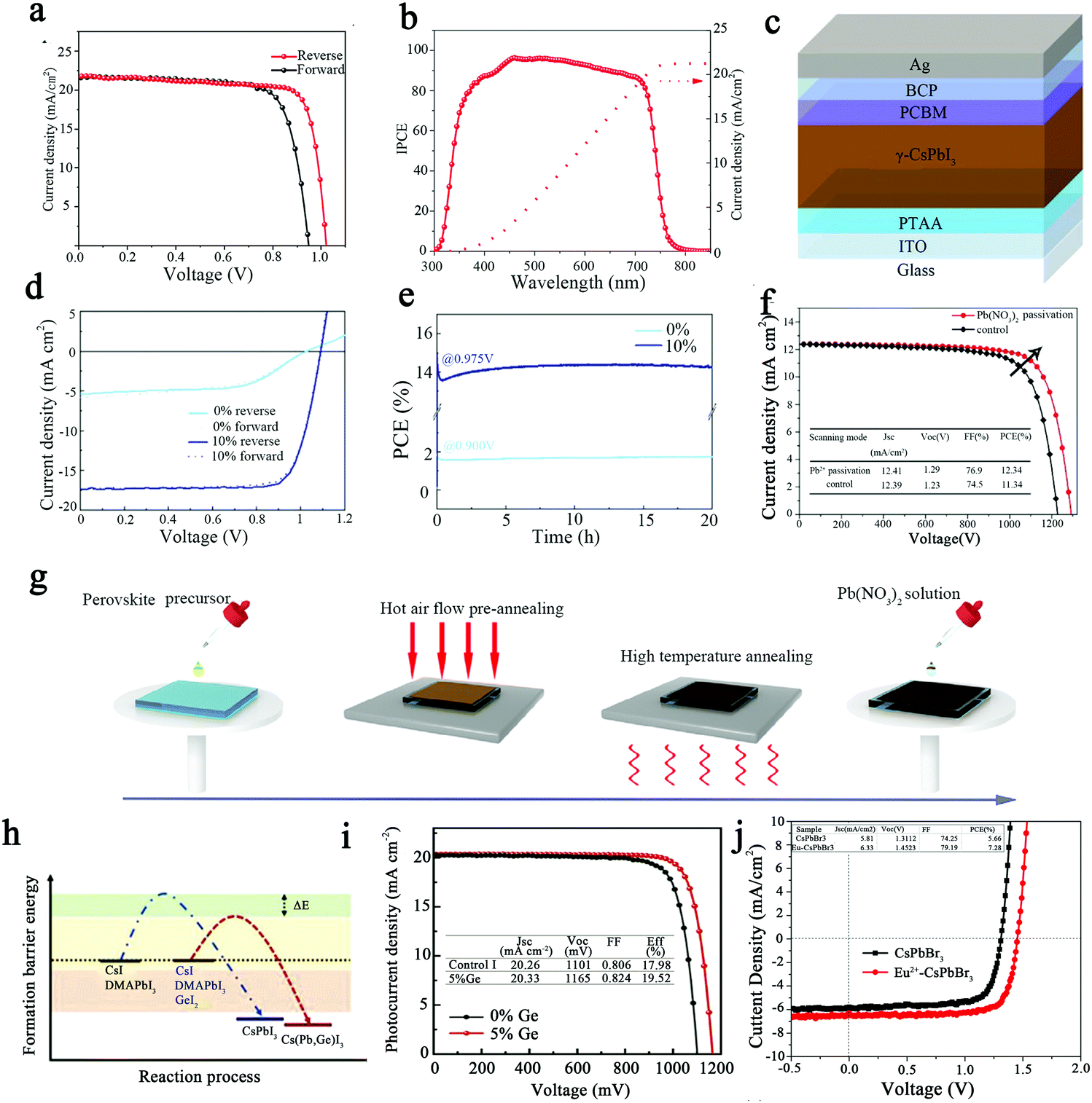 | ||
| Fig. 8 (a) J–V curve of FA0.15Cs0.85PbI3 solar cells.4 (b) EQE curves of FA0.15Cs0.85PbI3 solar cells.4 Copyright 2020, Wiley-Blackwell. (c) Structure of a CsPbI3 perovskite solar cell.21 (d) J–V characteristics of CsPbI3 (0%) and CsPbI3 with a 10% PEAI device.21 (e) PCE of CsPbI3 (0%) and CsPbI3 with a 10% PEAI device.21 Copyright 2021, Wiley-VCH Verlag. (f) J–V curves for the passivated CsPbI2Br devices and control devices.32 (g) Schematic diagram of the fabrication of perovskite films and the passivation process using Pb(NO3)2 ethyl acetate solution.32 Copyright 2018, Wiley-Blackwell. (h) Schematic diagram of the crystallization kinetics of CsPbI3 and Ge-doped CsPbI3 thin films.38 (i) J–V curves of the champion CsPb0.95Ge0.05I3-based PSC and control group.38 Copyright 2021, Wiley-VCH Verlag. (j) J–V curves of CsPbBr3 and Eu2+-doped CsPbBr3-based PSC.42 Copyright 2020, Wiley-Blackwell. | ||
In the second section of this paper, the preparation of CsPbX3 perovskite by thermal evaporation is presented, and the solution-processed devices in the field of photovoltaics usually are significantly better than those fabricated by thermal evaporation. Nevertheless, Zhang et al. prepared high-quality γ-CsPbI3 perovskite layers with PCEs of up to 15% by thermal evaporation of PbI2 and CsI with a small amount of phenylethylammonium iodide (PEAI), exceeding the performance of most solution-processed inorganic CsPbX3 (X = Cl, Br, I) PEAI perovskite solar cells.21Fig. 8c shows the structure of the CsPbI3 solar cell. The addition of the appropriate amount of PEAI not only provided high-quality perovskite films but also ensured charge transport in the active layer of the perovskite films, which exhibited a longer charge recombination lifetime; this indicates that the charge recombination is strongly suppressed, thus improving the performance of the PSCs. Fig. 8d displays the current density–voltage (J–V) characteristics of the device with a VOC of 1.09 V, JSC of 17.33 mA cm2, and fill factor of 79.41%. When PEAI was added at 10%, the device obtained 15% PCE, as shown in Fig. 8e.
Traps on the surface of perovskite can affect the conversion efficiency of perovskite solar cells. In recent years, some scholars have used post-treatment methods to reduce surface traps to further improve the PCE of inorganic PSCs. Yuan et al. introduced a Pb2+ solution post-processing strategy to passivate the deep trap state of CsPbI2Br films and obtained PSCs with a PCE of 12.34%.32 The dissociative Pb2+ in the solution can combine with the excess halide ions on the surface of perovskite, thus reducing the deep trap density of states and charge recombination. The reduction of defect states results in doubling of the average lifetime of perovskite, increasing the VOC and PCE of the solar cell device. The preparation and passivation process of CsPbI2Br perovskite films is shown in Fig. 8g. The structure of the planar heterojunction perovskite solar cells is in the form of FTO/SnO2/perovskite/spiro-OMeTAD/Ag. SnO2 is used as an electron transport layer to reduce the hysteresis effect, resulting in a JSC of 12.41 mA cm2, VOC of 1.29 V, and FF of 76.9% for perovskite solar cells, as shown in Fig. 8f. In addition, Li et al. synthesized n-methyl-2-pyrrolidinone iodide (NMPI) as a functional precursor additive to improve the phase stability and optical properties of CsPbI3.82 As a result, the PCE of the quasi-2D (n = 20) CsPbI3 PSC was increased to 14.59%, and the stability was significantly enhanced.
Doping has been used to participate in the crystallization process, altering the energy state of the perovskite and promoting the stability of the PSCs. Meng et al. found that Ge doping was able to modify the crystalline growth of CsPb1−xGexI3 films and reduce the annealing temperature and processing time by lowering the CsPbI3 formation energy.38 As shown in Fig. 8h, the first addition of Ge to the precursor of DMAPbI3 accelerated the crystallization process by lowering the formation energy and improving the thermodynamic stability. The GeO2 generated in situ on the surface of the perovskite film acts as a passivation layer to passivate the grain boundaries and surface defects, thereby improving the hygrothermal stability of the perovskite film and PSCs. The device structure of the solar cell is FTO/compact TiO2(c-TiO2)/PCBA/perovskite/spiro-OMeTAD/Au. As shown in Fig. 8i, the PCE of the best PSC is 19.52% (a certified PCE of 18.8%) with a JSC of 20.33 mA cm−2, VOC of 1165 mV, and FF of 0.824. Karunakaran et al. doped Eu2+ into all-inorganic CsPbBr3 PSCs, leading to an increase in PCE from 5.66% to 7.28%.42 Owing to the addition of rare earth elements, the perovskite films displayed crystallinity and smooth morphology while optimizing the charge transfer kinetics within the perovskite films. As shown in Fig. 8j, the photovoltaic performance was greatly improved when Eu2+ was introduced up to 60 μL.
This section focuses on the enhancement of the performance of all-inorganic PSCs by doping, which passivates the surface defects of perovskite and improves the average lifetime, thus optimizing the performance of PSCs. At the end of this section, some of the advances in CsPbX3 perovskite solar cells reported in the literature are summarized in Table 2.
| Materials | J SC (mA cm2) | V OC (V) | FF (%) | PCE (%) | Ref. |
|---|---|---|---|---|---|
| FA0.15Cs0.85PbI3 | 21.4 | 1.02 | 80 | 17.5 | 4 |
| CsPbX3 | 17.33 | 1.09 | 79.41 | 15 | 21 |
| CsPbI2Br | 12.41 | 1.29 | 76.90 | 12.34 | 32 |
| CsPbX3 | 12.6 | 1.05 | 78.70 | 10.40 | 83 |
| CsPbI3 | 15.68 | 1.20 | 64 | 12.04 | 84 |
| CsPbI2Br | 15.34 | 1.32 | 80 | 16.14 | 85 |
| CsPbI2Br | 15.23 | 1.14 | 64.51 | 11.20 | 86 |
| CsPbI3 | 0.415 | 0.643 | 42.9 | 0.11 | 87 |
| CsPbBr3 | 2.96 | 0.851 | 44.5 | 1.21 | 87 |
| CsPb1−xGexI3 | 20.33 | 1.165 | 82.4 | 18.8 | 38 |
| CsPbBr3 | 6.33 | 1.4523 | 79.19 | 7.28 | 42 |
3.2 Light-emitting diodes
Recently, increasing numbers of scholars have applied all-inorganic perovskite as light-emitting materials in LEDs. Next, we describe the application of perovskite with different luminescent colors in LEDs. The PN junctions are the basis for LEDs, where electrons and holes will migrate directionally and recombine near the PN junction when a forward bias is applied, releasing heat or light.88 Tang et al. prepared CsPbBr3 green-emitting LEDs by all-vacuum processing, and high-throughput combination strategies were adopted to optimize the perovskite composition, annealing temperature and functional layer thickness.8 The structure of CsPbBr3 perovskite LED is indium-doped tin oxide (ITO)/LiF/perovskite/TPBi/LiF/Al, and the energy band diagram of the AVBD-processed device is shown in Fig. 8a. When the Cs/Pb ratio and the thickness of the perovskite film are 1.17:1 and 110.6 nm, the LED will achieve optimal performance. The appropriate functional layer thickness can balance electron and hole injection, thus enhancing the EQE of the LED performance. The best device showed a current efficiency (CE) of 4.8 cd A−1 (EQE of 1.45%) at 2358 cd m−2, as shown in Fig. 9a. In addition, the CE improved to 10.15 cd A−1 and the EQE improved to 3.26% for perovskite LEDs by improving the hole-injection layer to NiOx. CsPbX3 perovskite is usually prepared in an inert environment under high temperature conditions, which hinders the large-scale production of LED devices, and a low-temperature preparation strategy is essential. Wang et al. synthesized CsPbBr3 NCs in the presence of the short-chain ligands propionic acid (PA) and butylamine (BLA) in a room temperature environment.20 In addition, studies have shown that CsPbBr3 NCs anchored by OA and OAm produce the best performance. Fig. 9b shows the energy level diagram of the CsPbBr3 LED and the structural composition of each part of the device. Fig. 9c demonstrates that the LEDs with OA/OAm-anchored NCs exhibit the best performance over a wide range, with a luminance of 5033 Cd m−2, CE of 18.6 Cd A−1, turn-on voltage as low as 3.2 V, and EQE of 5.4%.
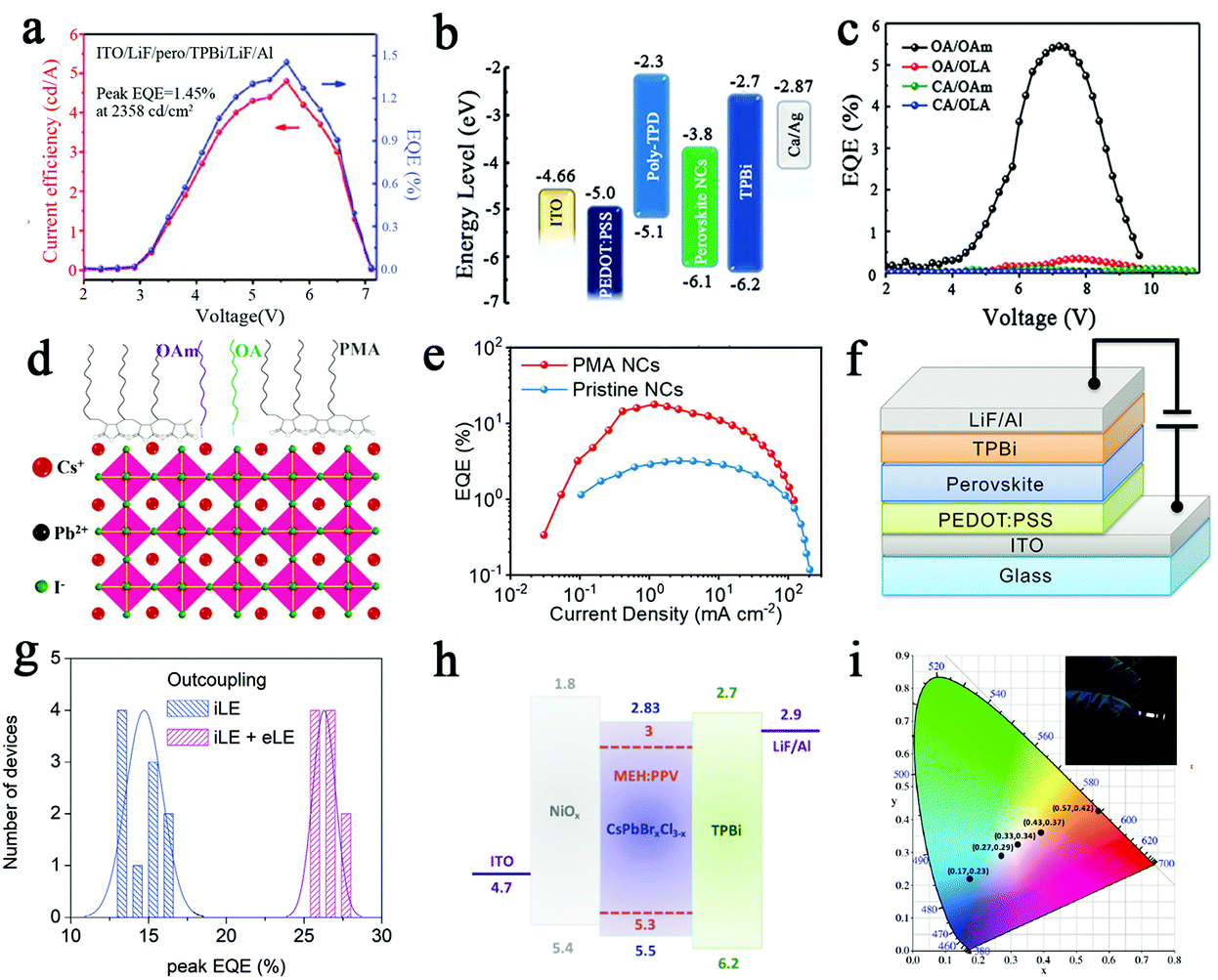 | ||
| Fig. 9 (a) Current efficiency and EQE curves of the best device.8 Copyright 2019, Wiley-VCH Verlag. (b) Energy level diagram of LED devices.20 (c) External quantum efficiency versus voltage of LED devices.20 Copyright 2019, Wiley-Blackwell. (d) Schematic diagram of the PMA-incorporating β-CsPbI3 NCs.27 (e) Relationship between the current density and EQE curve of the CsPbI3 LED.27 Copyright 2020, Wiley-Blackwell. (f) Schematic diagram of the structure of the PSC devices.33 (g) Histogram of the EQEs of the devices.33 Copyright 2021, Wiley-VCH Verlag. (h) Schematic of the band structure.39 (i) CIE coordinates of the white LED.39 Copyright 2016, Wiley-Blackwell. | ||
The stability of perovskite LEDs has been a great challenge, especially as red perovskite LEDs typically have a lifetime of only a few hours. Li et al. have prepared stable β-CsPbI3 for red-emitting LED applications through incorporation of poly(maleicanhydride-alt-1-octadecene) (PMA) in synthesizing the nanocrystals.27 As shown in Fig. 9d, the PMA can interact with PbI2 in the precursor through the coupling between the O group in PMA and Pb2+, and the PMA greatly passivated PbCs anti-situ defects on the surface of β-CsPbI3, which improved the stability of the crystal. The photoluminescence quantum yield of the β-CsPbI3 NCs films was significantly increased from 34% to 89% due to the addition of PMA. The structure of this device is indium tin oxide (ITO)/poly(3,4-ethylenedioxythiophene) polystyrene sulfonate (PEDOT:PSS)/poly-TPD/β-CsPbI3 NCs/tris(1-phenyl-1H-benzimidazole) (TPBi)/lithium fluoride (LiF)/Al. Fig. 9e shows red-emitting LEDs obtaining an EQE of 17.8%. The LEDs were stable for 317 h at a constant current density of 30 mA cm−2. Miao et al. prepared γ-CsPbI3 cuboid crystallites of deep red light perovskite LEDs based on a one-step method.89 Due to the addition of diammonium iodide to passivate the trap state of the in situ formed γ-CsPbI3, the high peak external quantum efficiency (EQE) value of the LED was 15.03%. Moreover, this one-step method offers a new strategy for the flow-line production of large-area perovskite LED modules.
Most of the current research on perovskite blue-emitting LEDs has been prepared by adjusting the band gap of a mixture of Br and I halogens. However, the film morphology of the mixed halide perovskite has not been well improved. Yao et al. prepared blue-emitting (470 nm) perovskite nanocrystals by mixing a 2:1 weight ratio of CsPbBr3 and CsPbI3 nanocrystals.39 By controlling the size of the thin film grains, high quality blue-emitting perovskite LEDs were obtained. Shen et al. proposed a simple device architecture to achieve highly efficient blue-emitting perovskite LEDs.33 Interfacial engineering is employed to manipulate the perovskite crystallization to achieve highly compact perovskite nanocrystals. The device structure of the blue perovskite LEDs is shown in Fig. 9f. On this basis, the EQE is further increased from 16.8% to 27.5% by integrating a lens-based structure for substrate mode light (Fig. 9g).
The preparation process of white perovskite LEDs is more complex than that of red, blue and green LEDs. Yao et al., mentioned in the previous paragraph, prepared a white light perovskite LED by mixing an orange light polymer with blue perovskite as the active layer.39 The device structure of white LEDs with a composite orange polymer material is shown in Fig. 9h. By adjusting the ratio between perovskite nanocrystals and polymers, white LEDs were achieved with CIE coordinates at (0.33, 0.34). Chen et al. first prepared red-emitting CsPbBr2.5I0.5 perovskite films by a one-step spin-coating method using polyacrylonitrile (PAN) polymer.90 Then, white LEDs were prepared by combining N,N′-bis(naphthalen-1-yl)-N,N′-bis(phenyl)-benzidine (NPB), CsPbBr2.5I0.5 perovskite films doped with PAN, and CsPbBr3. As shown in Fig. 9i, the LEDs displayed a maximum of 360 cd m−2 with CIE coordinates of (0.31, 0.36) at 7 V.
For further study, some optical parameters of CsPbX3 perovskite-based LEDs are summarized in Table 3. In recent years, many different methods of preparing perovskite LEDs have emerged, gradually improving their luminescence properties and stability. All-inorganic perovskite LEDs show great promise in the field of optical displays.
| Materials | Luminous colours | EL λmax (nm) | V on (V) | Max. EQE (%) | Max. CE (cd A−1) | Max. L (cd m−2) | Ref. |
|---|---|---|---|---|---|---|---|
| CsPbBr3 | Green | 523–524 | 3.92 | — | 1.07 | 1607 | 62 |
| CsPbBr3 | Green | 516 | — | 1.45 | 4.8 | 2358 | 8 |
| CsPbBr3 | Green | 516 | 3.2 | 5.4 | 18.6 | 5033 | 20 |
| CsPbBr3 | Green | 514 | — | 13.14 | 37.14 | 45990 |
26 |
| CsPbBr3 | Green | 517 | 2.3 | 5.7 | 19.9 | 46000 |
91 |
| CsPbBr3 | Green | 516 | 4.2 | 0.12 | 0.43 | 946 | 50 |
| CsPbI3 | Green | 586 | 4.6 | 0.09 | 0.08 | 528 | 50 |
| CsPbCl3 | Green | 455 | 5.1 | 0.07 | 0.14 | 742 | 50 |
| CsPbBr3 | Green | — | — | 0.25 | 0.96 | 637 | 92 |
| CsPbBr3 | Green | 510 | 2–2.5 | 0.37 | 0.72 | 1661 | 93 |
| CsPbI3 | Red | 689 | 5 | 17.8 | — | 618 | 27 |
| CsPbI3 | Red | 699 | 2.8 | 15.3 | — | 1272 | 89 |
| CsPbBrxCl3−x | Blue | 470 | 5 | 0.07 | 0.18 | 350 | 39 |
| CsPbBr3−xClx | Blue | 486 | 3.3 | 27.5 | 33.4 | 3651 | 33 |
| CsPb(Br2.5I0.5) + CsPbBr3 | White | — | 7 | — | 0.2 | 360 | 90 |
| CsPbBrxCl3−x + MEH:PPV | White | — | 8 | — | — | — | 39 |
3.3 Photodetectors
CsPbX3 perovskite is used in photodetectors due to its high light absorbance and long carrier diffusion length. Next, we describe the application of different structures of perovskite in photodetectors. Zeng et al. prepared CsPbBr3 nanosheets by improving the hot injection method and applied them in photodetectors.3 As shown in Fig. 10a, the edge length of the nanosheet could be greater than 1.5 μm. Large-area CsPbBr3 nanosheet films were prepared by simple ink printing or the roll-to-roll method and applied to flexible photodetectors, as shown in Fig. 10b. In the presence of an external electric field, the electron-hole pairs generated in the perovskite are rapidly separated and collected by the copper electrode, and then the CsPbBr3 nanosheet photodetector can work effectively. As shown in Fig. 10c, the maximum value of the responsivity was located at 517 nm, and the responsivity was 0.64 A W−1; the peak EQE value of the device at 515 nm was 53% at 10 V bias. A visible photodetector prepared using CsPbBr3 nanosheets exhibited a high sensitivity with a light on/off ratio of >103 under 442 nm light at a power of 0.35 mW cm−2 as well as high stability and outstanding fluorescence excitability (>10000 cycles). In addition, high stability and outstanding fluorescence excitability were still demonstrated after 10000 cycles.
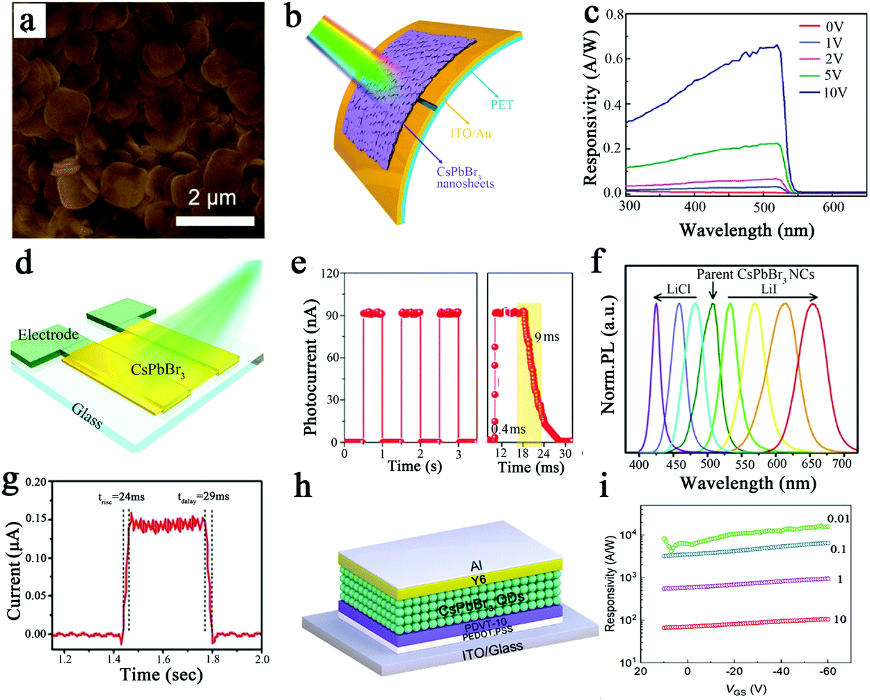 | ||
| Fig. 10 (a) SEM images of CsPbBr3 nanosheets.3 (b) Schematic diagram of PDs based on CsPbBr3 nanosheets.3 (c) Responsivity of CsPbBr3 nanosheet photodetector devices under different forward biases.3 Copyright 2016, Wiley-Blackwell. (d) Schematic of the photodetector device structure.23 (e) Left: Time-dependent optical response of the photoelectric detector. Right: Rise time and decay time of the photodetector under 530 nm light (216 μW m−2) at a bias of 2 V.23 Copyright 2018, Wiley-Blackwell. (f) PL spectra of CsPbBr3 NCs exchanged with different concentrations of LiI and LiCl.31 (g) Rise and decay times of the photodetector device.31 Copyright 2016, Royal Society of Chemistry. (h) Schematic device structure of the CsPbBr3 QDs/PDVT-10 phototransistor.37 (i) Responsivity of CsPbBr3 QDs/PDVT-10 phototransistors.37 Copyright 2021, Wiley-VCH Verlag. | ||
Large perovskite single crystals have the potential to produce high performance photodetectors due to their higher carrier mobility, longer diffusion length and longer carrier lifetime. Zheng et al. demonstrated a low-temperature and substrate-independent strategy to prepare millimeter-scale CsPbBr3 perovskite single-crystal films.23Fig. 10d shows a schematic of the device structure. The superior carrier transport properties will improve the performance of the photodetector. The trap density, diffusion length and migration lifetime of CsPbBr3 films and CsPbBr3 bulk crystals are comparable, but the resistivity is superior to that of the CsPbBr3 bulk crystals, which improves the performance of the photodetector. Fig. 10e shows the photodetector with a light on/off ratio >103 and rise and decay times of 0.4 ms and 9 ms, respectively. The CsPbBr3 films showed no significant photoluminescence loss after two months of storage, indicating that they exhibited excellent long-term stability to humidity and heat treatment. Ramasamy et al. prepared CsPbX3 (X = Cl, Br, I) nanocrystals (NCs) using halide ion exchange reactions at room temperature, and the photoluminescence could be tuned throughout the visible region (425–655 nm).31 In this report, CsPbBr3 perovskite colloidal NCs prepared by halogen exchange reactions were applied to photodetectors for the first time. An adjustable luminescence range was achieved through the halide ion exchange reactions. The green emission from CsPbBr3 NCs was tuned by lithium salts (LiX, X = I, Cl, Br) in the entire visible spectral region (425–655 nm) at room temperature. Fig. 10f demonstrates that different concentrations of lithium salts can tune the PL peak from 508 to 654 nm. The group selected CsPbI3 NCs with relatively long radiation lifetimes for photodetector applications. The CsPbI3 photodetector exhibits an excellent on/off photocurrent ratio of 105. In addition, the CsPbI3 photodetector showed a relatively fast rise time (trise = 24 ms) and decay time (tdecay = 29 ms), as shown in Fig. 10g.
Planar heterojunction (PHJ) structures consisting of different semiconductors also show great potential in photodetectors. Chen et al. prepared solution-processed perovskite quantum dots (PQDs)/organic semiconductors (OSC) planar heterojunctions and applied them to photodetectors.37 CsPbBr3 QDs were prepared by the hot-injection method, and the quantum dot films were prepared by spin coating. Fig. 10h shows a schematic of the phototransistor for CsPbBr3 QDs/PDVT-10 PHJs. As shown in Fig. 10i, the R-value can reach 1.64 × 10⁴ A W−1 when the illumination intensity is 0.01 mW cm−2. In addition, the double layer PQD/PDVT-10 PHJs phototransistor has a specific detectivity of 3.17 × 10¹² Jones and a photosensitivity of 5.33 × 10⁶. The presence of the PHJ structure allows the exciton dissociation process to become more efficient. This photosensitive effect is important for achieving high responsiveness or gain in PHJ-based phototransistors due to the extended excess carrier lifetime. For comparison, the properties of CsPbX3 perovskite PDs are summarized in Table 4.
| Materials | Shapes | Responsivity (A W−1) | On/off ratio | Rise time (ms) | Decay time (ms) | EQE (%) | Ref. |
|---|---|---|---|---|---|---|---|
| CsPbBr3 | Nanosheet | 0.64 | >104 | 0.019 | 0.24 | 54 | 3 |
| CsPbBr3–CNTs | Nanosheet | 31.1 | >832 | 0.016 | 0.38 | — | 95 |
| CsPbBr3 | Film | 0.21 | 103 | 0.4 | 9 | 6.2 | 23 |
| CsPbBr3/ZnO | Film | 4.25 | >104 | 0.21 | 0.24 | — | 96 |
| CsPbI3 | Nanocrystal | — | 105 | 24 | 29 | — | 31 |
4. Conclusions
In summary, here, we reviewed some advances in OIH perovskites, mainly some different preparation methods of all-inorganic perovskites and their applications in optoelectronic fields. Recently, due to the special physical structure and excellent optical properties of CsPbX3 perovskite, researchers have conducted extensive research on CsPbX3. However, there are still some challenges in the practical application of perovskite remaining to be addressed. Therefore, in this section, we focus on a summary of the current challenges and opportunities for perovskite applications.Firstly, the toxicity of lead halide perovskite needs to be considered. The heavy metal ion lead has severe consequences on human health and the environment. Appropriate encapsulation strategies are needed to reduce the toxicity of lead halide perovskite. When the lead halide perovskite encapsulated by the polymer is exposed to water, the lead concentration is comparable to that in tap water. Another alternative solution is the development of lead-free halide perovskite, a non-toxic element (such as Sn, Bi, Sb, Cu, and Ge) to replace the toxic lead.94
Secondly, the instability of the internal structure of perovskite is also a problem that limits its commercialization. The water stability of perovskite has been improved through different approaches, including surface passivation and the polymer encapsulation strategy. However, polymer encapsulation can affect the electrical properties of perovskites, reducing the efficiency of their optoelectronic devices. Subsequent research needs to focus on surface modification, improvement of surface passivation strategies or improvement of chemical components.
Third, compared to OIH perovskites, the band gap of all-inorganic perovskites should be suitably adjusted to better improve the performance of optoelectronic devices. Therefore, the band gap of all-inorganic perovskites is tuned and their stability is further improved by doping, metal-organic framework crystal embedding and ligand-based studies.
Ultimately, we hope that theoretical calculations and experiment studies in CsPbX3 will be of great benefit to the synthesis of crystals and device performance. All-inorganic perovskites still have a long way to go, but we believe that they will make great progress in a variety of applications. CsPbX3 can play important roles in photovoltaics and improving human well-being.
Conflicts of interest
There are no conflicts to declare.Acknowledgements
This work was supported by the National Science Foundation of China (No. 61904123), the Natural Science Foundation of Tianjin (No. 18JCQNJC71800), Scientific Research Project of Tianjin Educational Committee (No. 2018KJ220), Tianjin Technical and Engineering Center of Nonwovens (No. KF202103).Notes and references
- M. Z. Liu, M. B. Johnston and H. J. Snaith, Efficient planar heterojunction perovskite solar cells by vapour deposition, Nature, 2013, 501(7467), 395–398 CrossRef CAS PubMed.
- J. Shamsi, A. S. Urban, M. Imran, L. De Trizio and L. Manna, Metal Halide Perovskite Nanocrystals: Synthesis, Post-Synthesis Modifications, and Their Optical Properties, Chem. Rev., 2019, 119(5), 3296–3348 CrossRef CAS.
- J. Z. Song, L. M. Xu, J. H. Li, J. Xue, Y. H. Dong, X. M. Li and H. B. Zeng, Monolayer and Few-Layer All-Inorganic Perovskites as a New Family of Two-Dimensional Semiconductors for Printable Optoelectronic Devices, Adv. Mater., 2016, 28(24), 4861–4869 CrossRef CAS PubMed.
- Z. P. Shao, H. G. Meng, X. F. Du, X. H. Sun, P. L. Lv, C. Y. Gao, Y. Rao, C. Chen, Z. P. Li, X. Wang, G. L. Cui and S. P. Pang, Cs4PbI6-Mediated Synthesis of Thermodynamically Stable FA(0.15)Cs(0.85)PbI(3)Perovskite Solar Cells, Adv. Mater., 2020, 32(30) DOI:10.1002/adma.202001054.
- D. H. Jiang, Y. H. Tsai, L. Veeramuthu, F. C. Liang, L. C. Chen, C. C. Lin, T. Satoh, S. H. Tung and C. C. Kuo, Novel ultra-stable and highly luminescent white light-emitting diodes from perovskite quantum dots-Polymer nanofibers through biaxial electrospinning, Appl. Mater., 2019, 7(11) DOI:10.1063/1.5124880.
- J. Z. Song, Q. Z. Cui, J. H. Li, J. Y. Xu, Y. Wang, L. M. Xu, J. Xue, Y. H. Dong, T. Tian, H. D. Sun and H. B. Zeng, Ultralarge All-Inorganic Perovskite Bulk Single Crystal for High-Performance Visible-Infrared Dual-Modal Photodetectors, Adv. Opt. Mater., 2017, 5(12) DOI:10.1002/adom.201700157.
- J. J. Ren, T. R. Li, X. P. Zhou, X. Dong, A. V. Shorokhov, M. B. Semenov, V. D. Krevchik and Y. H. Wang, Encapsulating all-inorganic perovskite quantum dots into mesoporous metal organic frameworks with significantly enhanced stability for optoelectronic applications, Chem. Eng. J., 2019, 358, 30–39 CrossRef CAS.
- J. H. Li, P. P. Du, S. R. Li, J. Liu, M. H. Zhu, Z. F. Tan, M. C. Hu, J. J. Luo, D. Q. A. Guo, L. Ma, Z. G. Nie, Y. Ma, L. Gao, G. D. Niu and J. Tang, High-Throughput Combinatorial Optimizations of Perovskite Light-Emitting Diodes Based on All-Vacuum Deposition, Adv. Funct. Mater., 2019, 29(51) DOI:10.1002/adfm.201903607.
- N. Lakhdar and A. Hima, Electron transport material effect on performance of perovskite solar cells based on CH3NH3GeI3., Opt. Mater., 2020, 99 Search PubMed.
- J. Y. Guan, J. Ni, X. J. Zhou, Y. Liu, J. Y. Yin, J. L. Wang, D. Wang, Y. F. Zhang, J. Li, H. K. Cai and J. J. Zhang, High-Performance Electron Transport Layer via Ultrasonic Spray Deposition for Commercialized Perovskite Solar Cells, ACS Appl. Energy Mater., 2020, 3(12), 11570–11580 CrossRef CAS.
- H. Sung, N. Ahn, M. S. Jang, J. K. Lee, H. Yoon, N. G. Park and M. Choi, Transparent Conductive Oxide-Free Graphene-Based Perovskite Solar Cells with over 17% Efficiency, Adv. Energy Mater., 2016, 6(3) DOI:10.1002/aenm.201501873.
- J. H. Heo and S. H. Im, CH3NH3PbBr3–CH3NH3PbI3 Perovskite-Perovskite Tandem Solar Cells with Exceeding 2.2 V Open Circuit Voltage, Adv. Mater., 2016, 28(25), 5121–5125 CrossRef CAS PubMed.
- M. A. Green, A. Ho-Baillie and H. J. Snaith, The emergence of perovskite solar cells, Nat. Photonics, 2014, 8(7), 506–514 CrossRef CAS.
- H. Tang, S. S. He and C. W. Peng, A Short Progress Report on High-Efficiency Perovskite Solar Cells, Nanoscale Res. Lett., 2017, 12 Search PubMed.
- G. A. Al-Dainy, S. E. Bourdo, V. Saini, B. C. Berry and A. S. Biris, Hybrid Perovskite Photovoltaic Devices: Properties, Architecture, and Fabrication Methods, Energy Technology, 2017, 5(3), 373–401 CrossRef CAS.
- J. Lei, F. Gao, H. X. Wang, J. Li, J. X. Jiang, X. Wu, R. R. Gao, Z. Yang and S. Z. Liu, Efficient planar CsPbBr3 perovskite solar cells by dual-source vacuum evaporation, Solar Energy Mater. Solar Cells, 2018, 187, 1–8 CrossRef CAS.
- L. Protesescu; S. Yakunin; M. I. Bodnarchuk; F. Krieg; R. Caputo; C. H. Hendon; R. X. Yang; A. Walsh and M. V. Kovalenko, Nanocrystals of Cesium Lead Halide Perovskites (CsPbX3, X = Cl, Br, and I): Novel Optoelectronic Materials Showing Bright Emission with Wide Color Gamut. Nano Lett. 2015, 15 (6), 3692–3696 Search PubMed.
- Y. P. Fu, H. M. Zhu, C. C. Stoumpos, Q. Ding, J. Wang, M. G. Kanatzidis, X. Y. Zhu and S. Jin, Broad Wavelength Tunable Robust Lasing from Single-Crystal Nanowires of Cesium Lead Halide Perovskites (CsPbX3, X = Cl, Br, I), ACS Nano, 2016, 10(8), 7963–7972 CrossRef CAS PubMed.
- H. Liao, S. B. Guo, S. Cao, L. Wang, F. M. Gao, Z. B. Yang, J. J. Zheng and W. Y. Yang, A General Strategy for In Situ Growth of All-Inorganic CsPbX3 (X = Br, I, and Cl) Perovskite Nanocrystals in Polymer Fibers toward Significantly Enhanced Water/Thermal Stabilities, Adv. Opt. Mater., 2018, 6(15) DOI:10.1002/adom.201800346.
- F. H. Ye, H. J. Zhang, W. Li, Y. Yan, J. L. Cai, R. S. Gurney, A. J. Pearson, D. Liu and T. Wang, Ligand-Exchange of Low-Temperature Synthesized CsPbBr3 Perovskite toward High-Efficiency Light-Emitting Diodes, Small Methods, 2019, 3(3) DOI:10.1002/smtd.201800489.
- Z. B. Zhang, R. Ji, M. Kroll, Y. J. Hofstetter, X. K. Jia, D. Becker-Koch, F. Paulus, M. Loffler, F. Nehm, K. Leo and Y. Vaynzof, Efficient Thermally Evaporated gamma-CsPbI3 Perovskite Solar Cells, Adv. Energy Mater., 2021, 11(29) DOI:10.1002/aenm.202100299.
- K. Wang, L. Y. Zheng, T. Zhu, X. Yao, C. Yi, X. T. Zhang, Y. Cao, L. Liu, W. P. Hu and X. Gong, Efficient perovskite solar cells by hybrid perovskites incorporated with heterovalent neodymium cations, Nano Energy, 2019, 61, 352–360 CrossRef CAS.
- Z. Yang, Q. Xu, X. D. Wang, J. F. Lu, H. Wang, F. T. Li, L. Zhang, G. F. Hu and C. F. Pan, Large and Ultrastable All-Inorganic CsPbBr3 Monocrystalline Films: Low-Temperature Growth and Application for High-Performance Photodetectors., Adv. Mater., 2018, 30(44) DOI:10.1002/adma.201802110.
- J. Liang, J. Liu and Z. Jin, All-Inorganic Halide Perovskites for Optoelectronics: Progress and Prospects, Solar Rrl, 2017, 1(10) DOI:10.1002/solr.201700086.
- Y. B. Zhao, C. Xie, X. Zhang and P. Yang, CsPbX3 Quantum Dots Embedded in Zeolitic Imidazolate Framework-8 Microparticles for Bright White Light-Emitting Devices, ACS Appl. Nano Mater., 2021, 4(5), 5478–5485 CrossRef CAS.
- L. P. Cheng, J. S. Huang, Y. Shen, G. P. Li, X. K. Liu, W. Li, Y. H. Wang, Y. Q. Li, Y. Jiang, F. Gao, C. S. Lee and J. X. Tang, Efficient CsPbBr3 Perovskite Light-Emitting Diodes Enabled by Synergetic Morphology Control, Adv. Opt. Mater., 2019, 7(4) DOI:10.1002/adom.201801534.
- H. M. Li, H. Lin, D. Ouyang, C. L. Yao, C. Li, J. Y. Sun, Y. L. Song, Y. F. Wang, Y. F. Yan, Y. Wang, Q. F. Dong and W. C. H. Choy, Efficient and Stable Red Perovskite Light-Emitting Diodes with Operational Stability >300 h, Adv. Mater., 2021, 33(15) DOI:10.1002/adma.202008820.
- M. Imran, V. Caligiuri, M. J. Wang, L. Goldoni, M. Prato, R. Krahne, L. De Trizio and L. Manna, Benzoyl Halides as Alternative Precursors for the Colloidal Synthesis of Lead-Based Halide Perovskite Nanocrystals, J. Am. Chem. Soc., 2018, 140(7), 2656–2664 CrossRef CAS PubMed.
- W. W. Lai, C. L. Wu, W. H. Li and X. X. Han, Green solvent assisted preparation of one-dimensional CsPbBr3 nanocrystals with a controllable morphology for cyan-emitting applications, CrystEngComm, 2021, 23(44), 7805–7812 RSC.
- Y. B. Xue, Y. Y. Shan and H. Xu, First-principles study on the initial decomposition process of CH3NH3PbI3, J. Chem. Phys., 2017, 147(12) DOI:10.1063/1.4995496.
- P. Ramasamy, D. H. Lim, B. Kim, S. H. Lee, M. S. Lee and J. S. Lee, All-inorganic cesium lead halide perovskite nanocrystals for photodetector applications, Chem. Commun., 2016, 52(10), 2067–2070 RSC.
- J. F. Yuan, L. X. Zhang, C. H. Bi, M. R. Wang and J. J. Tian, Surface Trap States Passivation for High-Performance Inorganic Perovskite Solar Cells, Solar Rrl, 2018, 2(10) DOI:10.1002/solr.201800188.
- Y. Shen, H. Y. Wu, Y. Q. Li, K. C. Shen, X. Y. Gao, F. Song and J. X. Tang, Interfacial Nucleation Seeding for Electroluminescent Manipulation in Blue Perovskite Light-Emitting Diodes, Adv. Funct. Mater., 2021, 31(45) DOI:10.1002/adfm.202103870.
- W. Li, Z. M. Wang, F. Deschler, S. Gao, R. H. Friend and A. K. Cheetham, Chemically diverse and multifunctional hybrid organic–inorganic perovskites, Nat. Rev. Mater., 2017, 2(3) DOI:10.1038/natrevmats.2016.99.
- C. Chen, T. Han, S. Tan, J. J. Xue, Y. P. Zhao, Y. F. Liu, H. R. Wang, W. Hu, C. Bao, M. Mazzeo, R. Wang, Y. Duan and Y. Yang, Efficient Flexible Inorganic Perovskite Light-Emitting Diodes Fabricated with CsPbBr3 Emitters Prepared via Low-Temperature in Situ Dynamic Thermal Crystallization, Nano Lett., 2020, 20(6), 4673–4680 CrossRef CAS PubMed.
- S. Laalioui, K. B. Alaoui, H. A. Dads, K. El Assali, B. Ikken and A. Outzourhit, Progress in perovskite based solar cells: scientific and engineering state of the art, Rev. Adv. Mater. Sci., 2020, 59(1), 10–25 CAS.
- K. X. Chen, X. L. Zhang, P. A. Chen, J. Guo, M. He, Y. Q. Chen, X. C. Qiu, Y. Liu, H. J. Chen, Z. B. Zeng, X. Wang, J. Y. Yuan, W. L. Ma, L. Liao, T. Q. Nguyen and Y. Y. Hu, Solution-Processed CsPbBr3 Quantum Dots/Organic Semiconductor Planar Heterojunctions for High-Performance Photodetectors, Adv. Sci, 2022 DOI:10.1002/advs.202105856.
- F. Q. Meng, B. C. Yu, Q. H. Zhang, Y. Q. Cui, S. Tan, J. J. Shi, L. Gu, D. M. Li, Q. B. Meng and C. W. Nan, Ge Incorporation to Stabilize Efficient Inorganic CsPbI3 Perovskite Solar Cells, Adv. Energy Materi., 2022, 12(10) DOI:10.1002/aenm.202103690.
- E. P. Yao, Z. L. Yang, L. Meng, P. Y. Sun, S. Q. Dong, Y. Yang and Y. Yang, High-Brightness Blue and White LEDs based on Inorganic Perovskite Nanocrystals and their Composites, Adv. Mater., 2017, 29(23) DOI:10.1002/adma.201606859.
- N. J. Jeon, J. H. Noh, W. S. Yang, Y. C. Kim, S. Ryu, J. Seo and S. I. Seok, Compositional engineering of perovskite materials for high-performance solar cells, Nature, 2015, 517(7535), 476–480 CrossRef CAS PubMed.
- J. A. Schwenzer, T. Hellmann, B. A. Nejand, H. Hu, T. Abzieher, F. Schackmar, I. M. Hossain, P. Fassl, T. Mayer, W. Jaegermann, U. Lemmer and U. W. Paetzold, Thermal Stability and Cation Composition of Hybrid Organic–Inorganic Perovskites, ACS Appl. Mater. Interfaces, 2021, 13(13), 15292–15304 CrossRef CAS PubMed.
- S. K. Karunakaran, G. M. Arumugam, W. T. Yang, S. J. Ge, S. N. Khan, Y. H. Mai, X. Z. Lin and G. W. Yang, Europium(II)-Doped All-Inorganic CsPbBr3 Perovskite Solar Cells with Carbon Electrodes, Solar Rrl, 2020, 4(11) DOI:10.1002/solr.202000390.
- M. T. Weller, O. J. Weber, J. M. Frost and A. Walsh, Cubic Perovskite Structure of Black Formamidinium Lead Iodide, alpha- HC(NH2)(2)PbI3, at 298 K, J. Phys. Chem. Lett., 2015, 6(16), 3209–3212 CrossRef CAS.
- M. Kulbak, S. Gupta, N. Kedem, I. Levine, T. Bendikov, G. Hodes and D. Cahen, Cesium Enhances Long-Term Stability of Lead Bromide Perovskite-Based Solar Cells, J. Phys. Chem. Lett., 2016, 7(1), 167–172 CrossRef CAS PubMed.
- T. Guner, G. Topcu, U. Savaci, A. Genc, S. Turan, E. Sari and M. M. Demir, Polarized emission from CsPbBr3 nanowire embedded-electrospun PU fibers, Nanotechnology, 2018, 29(13) DOI:10.1088/1361-6528/aaaaef.
- X. Lu, Y. Hu, J. Z. Guo, C. F. Wang and S. Chen, Fiber-Spinning-Chemistry Method toward In Situ Generation of Highly Stable Halide Perovskite Nanocrystals, Adv. Sci., 2019, 6(22) DOI:10.1002/advs.201901694.
- J. Xu, Preparation of high-efficiency perovskite solar cells based on novel cavity transport materials, MS thesis, Harbin Institute of Technology, 2020 Search PubMed.
- Y. Huang, Q. D. Sun, W. Xu, Y. He and W. J. Yin, Halide Perovskite Materials for Solar Cells: a Theoretical Review, Acta Phys.-Chim. Sin., 2017, 33(9), 1730–1751 CAS.
- J. R. Zhang, G. Hodes, Z. W. Jin and S. Z. Liu, All-Inorganic CsPbX3 Perovskite Solar Cells: Progress and Prospects, Angew. Chem., Int. Ed., 2019, 58(44), 15596–15618 CrossRef CAS PubMed.
- J. Z. Song, J. H. Li, X. M. Li, L. M. Xu, Y. H. Dong and H. B. Zeng, Quantum Dot Light-Emitting Diodes Based on Inorganic Perovskite Cesium Lead Halides (CsPbX3), Adv. Mater., 2015, 27(44), 7162–7167 CrossRef CAS PubMed.
- X. M. Li, Y. Wu, S. L. Zhang, B. Cai, Y. Gu, J. Z. Song and H. B. Zeng, CsPbX3 Quantum Dots for Lighting and Displays: Room-Temperature Synthesis, Photoluminescence Superiorities, Underlying Origins and White Light-Emitting Diodes, Adv. Funct. Mater., 2016, 26(15), 2435–2445 CrossRef CAS.
- J. R. Zhu, X. L. Yang, Y. H. Zhu, Y. W. Wang, J. Cai, J. H. Shen, L. Y. Sun and C. Z. Li, Room-Temperature Synthesis of Mn-Doped Cesium Lead Halide Quantum Dots with High Mn Substitution Ratio, J. Phys. Chem. Lett., 2017, 8(17), 4167–4171 CrossRef CAS PubMed.
- Y. Su, X. J. Chen, W. Y. Ji, Q. H. Zeng, Z. Y. Ren, Z. S. Su and L. Liu, Highly Controllable and Efficient Synthesis of Mixed-Halide CsPbX3 (X = Cl, Br, I) Permiskite QDs toward the Tunability of Entire Visible Light, ACS Appl. Mater. Interfaces, 2017, 9(38), 33020–33028 CrossRef CAS PubMed.
- W. W. Chen, X. S. Tang, Z. G. Zang, Y. Shi, Z. Q. Yang and J. Du, Tunable dual emission in Mn2+-doped CsPbX3 (X = Cl, Br) quantum dots for high efficiency white light-emitting diodes, Nanotechnology, 2019, 30(7) DOI:10.1088/1361-6528/aaf299.
- Q. Y. Zhang, F. Y. Diao, X. Y. Xue, X. L. Sheng, D. Barba and Y. Q. Wang, Self-Assembly of CsPbBr3 Nanocubes into 2D Nanosheets, ACS Appl. Mater. Interfaces, 2021, 13(37), 44777–44785 CrossRef CAS PubMed.
- M. Jagadeeswararao, P. Vashishtha, T. J. N. Hooper, A. Kanwat, J. W. M. Lim, S. K. Vishwanath, N. Yantara, T. Park, T. C. Sum, D. S. Chung, S. G. Mhaisalkar and N. Mathews, One-Pot Synthesis and Structural Evolution of Colloidal Cesium Lead Halide-Lead Sulfide Heterostructure Nanocrystals for Optoelectronic Applications, J. Phys. Chem. Lett., 2021, 12(39), 9569–9578 CrossRef CAS PubMed.
- Y. Tong, Q. Wang, E. R. Mei, X. J. Liang, W. Gao and W. D. Xiang, One-Pot Synthesis of CsPbX3 (X = Cl, Br, I)@Zeolite: A Potential Material for Wide-Color-Gamut Backlit Displays and Upconversion Emission, Adv. Opt. Mater., 2021, 9(11) DOI:10.1002/adom.202100012.
- Y. Hu, Q. Wang, Y. L. Shi, M. Li, L. Zhang, Z. K. Wang and L. S. Liao, Vacuum-evaporated all-inorganic cesium lead bromine perovskites for high-performance light-emitting diodes, J. Mater. Chem. C, 2017, 5(32), 8144–8149 RSC.
- L. Zhang, F. Yuan, H. Dong, B. Jiao, W. W. Zhang, X. Hou, S. F. Wang, Q. H. Gong and Z. X. Wu, One-Step Co-Evaporation of All-Inorganic Perovskite Thin Films with Room-Temperature Ultralow Amplified Spontaneous Emission Threshold and Air Stability, ACS Appl. Mater. Interfaces, 2018, 10(47), 40661–40671 CrossRef CAS PubMed.
- T. Burwig, W. Franzel and P. Pistor, Crystal Phases and Thermal Stability of Co-evaporated CsPbX3 (X = I, Br) Thin Films, J. Phys. Chem. Lett., 2018, 9(16), 4808–4813 CrossRef CAS PubMed.
- P. P. Du, J. H. Li, L. Wang, J. Liu, S. R. Li, N. Liu, Y. X. Li, M. Y. Zhang, L. Gao, Y. Ma and J. Tang, Vacuum-Deposited Blue Inorganic Perovskite Light-Emitting Diodes, ACS Appl. Mater. Interfaces, 2019, 11(50), 47083–47090 CrossRef CAS PubMed.
- M. Shin, H. S. Lee, Y. C. Sim, Y. H. Cho, K. C. Choi and B. Shin, Modulation of Growth Kinetics of Vacuum-Deposited CsPbBr3 Films for Efficient Light-Emitting Diodes, ACS Appl. Mater. Interfaces, 2020, 12(1), 1944–1952 CrossRef CAS PubMed.
- H. M. Ghaithan, S. M. H. Qaid, Z. A. Alahmed, M. Hezam, A. Lyras, M. Amer and A. S. Aldwayyan, Anion Substitution Effects on the Structural, Electronic, and Optical Properties of Inorganic CsPb(I1−xBrx)(3) and CsPb(Br1−xClx)(3) Perovskites: Theoretical and Experimental Approaches, J. Phys. Chem. C, 2021, 125(1), 886–897 CrossRef CAS.
- S. Ullah, P. X. Yang, Y. Q. Li, J. M. Wang, L. L. Liu, R. Mahmood, S. E. Yang, T. Y. Xia, H. Z. Guo and Y. S. Chen, Two step vapor-processing and experimental investigations of all-inorganic CsPbCl3 perovskite films for optoelectronic applications, Mater. Lett., 2021, 294 Search PubMed.
- M. S. Yang, J. Yu, S. Z. Jiang, C. Zhang, Q. Q. Sun, M. H. Wang, H. Zhou, C. H. Li, B. Y. Man and F. C. Lei, High stability luminophores: fluorescent CsPbX3 (X = Cl, Br and I) nanofiber prepared by one-step electrospinning method, Opt. Express, 2018, 26(16), 20649–20660 CrossRef CAS PubMed.
- L. H. Zhang, Q. S. Sun, Y. K. Xu, L. L. Han, Q. Wang, Y. C. Yu, Z. W. Jin, S. K. Yang and Z. P. Ci, Self-assembled template-confined growth of ultrathin CsPbBr3 nanowires, Appl. Mater. Today, 2020, 18 Search PubMed.
- Y. J. Huang, T. T. Wang, J. Z. Zheng, F. M. Li, W. R. Lan, F. Y. Zheng and S. X. Li, Multiwalled Carbon Nanotubes/CsPbX3@Polyacrylonitrile Core/Shell Nanofibers with Ultrahigh Water, Thermal, and Ultraviolet Stability, Macromol. Mater. Eng., 2021, 306(10) DOI:10.1002/mame.202100200.
- W. N. Liu, H. Fu, H. Liao, Z. Liang, Y. M. Ye, J. J. Zheng and W. Y. Yang, In situ synthesis of coaxial CsPbX3@polymer (X = Cl, Br, I) fibers with significantly enhanced water stability, J. Mater. Chem. C, 2020, 8(40), 13972–13975 RSC.
- J. H. Cha, H. Kim, Y. Lee, S. J. Kim, M. W. Lee, J. Kim and D. Y. Jung, Nanoscale optical imaging of perovskite nanocrystals directly embedded in polymer fiber, Compos. Sci. Technol., 2019, 181 Search PubMed.
- K. J. Babu, G. Kaur, L. Biswal, G. De and H. N. Ghosh, Ultrafast Charge Delocalization Dynamics of Ambient Stable CsPbBr3 Nanocrystals Encapsulated in Polystyrene Fiber, Chem. – Eur. J., 2021, 27(2), 683–691 CrossRef CAS PubMed.
- S. Chan, M. N. Liu, K. Latham, M. Haruta, H. Kurata, T. Teranishi and Y. Tachibana, Monodisperse and size-tunable PbS colloidal quantum dots via heterogeneous precursors, J. Mater. Chem. C, 2017, 5(8), 2182–2187 RSC.
- J. Yao, All-Inorganic Lead Halide Perovskite Efficient Light Emitting Nanocrystals and Light Emitting Diode Devices, PhD thesis, University of Science and Technology of China, 2021 Search PubMed.
- W. W. Yu and X. G. Peng, Formation of high-quality CdS and other II–VI semiconductor nanocrystals in noncoordinating solvents: Tunable reactivity of monomers, Angew. Chem., Int. Ed., 2002, 41(13), 2368–2371 CrossRef CAS PubMed.
- A. Yan, Preparation, optical properties and LED applications of all-inorganic halide perovskite, PhD thesis, Wuhan University of Technology, 2020 Search PubMed.
- J. Fu, Shape control and its application in electrostatic spinning, PhD thesis, Lanzhou University, 2014 Search PubMed.
- S. He, Analysis and validation of the factors influencing the morphology of electrostatically spun nanofibers, PhD thesis, Donghua University, 2011 Search PubMed.
- L. B. Qiu, J. Deng, X. Lu, Z. B. Yang and H. S. Peng, Integrating Perovskite Solar Cells into a Flexible Fiber, Angew. Chem., Int. Ed., 2014, 53(39), 10425–10428 CrossRef CAS PubMed.
- Z. L. Zhang, Z. H. Chen, J. B. Zhang, W. J. Chen, J. F. Yang, X. M. Wen, B. Wang, N. Kobamoto, L. Yuan, J. A. Stride, G. J. Conibeer, R. J. Patterson and S. J. Huang, Significant Improvement in the Performance of PbSe Quantum Dot Solar Cell by Introducing a CsPbBr3 Perovskite Colloidal Nanocrystal Back Layer, Adv. Energy Mater., 2017, 7(5) DOI:10.1002/aenm.201601773.
- H. L. Wang, Z. J. Dong, H. C. Liu, W. P. Li, L. Q. Zhu and H. N. Chen, Roles of Organic Molecules in Inorganic CsPbX3 Perovskite Solar Cells, Adv. Energy Mater., 2021, 11(1) DOI:10.1002/aenm.202002940.
- Q. W. Zhou, J. L. Duan, J. Du, Q. Y. Guo, Q. Y. Zhang, X. Y. Yang, Y. Y. Duan and Q. W. Tang, Tailored Lattice “Tape” to Confine Tensile Interface for 11.08%-Efficiency All-Inorganic CsPbBr3 Perovskite Solar Cell with an Ultrahigh Voltage of 1.702 V, Adv. Sci., 2021, 8(19) DOI:10.1002/advs.202101418.
- C. K. Ng, W. P. Yin, H. C. Li and J. J. Jasieniak, Scalable synthesis of colloidal CsPbBr3 perovskite nanocrystals with high reaction yields through solvent and ligand engineering, Nanoscale, 2020, 12(8), 4859–4867 RSC.
- Z. Z. Li, B. Ma, Y. K. Xu, Y. T. Lei, W. Lan, G. Wang, W. Q. Li, Q. Wang, H. L. Zhang and Z. W. Jin, N-methyl-2-pyrrolidone Iodide as Functional Precursor Additive for Record Efficiency 2D Ruddlesden-Popper (PEA)(2)(Cs)(n)−1PbnI3n+1 Solar Cells, Adv. Funct. Mater., 2021, 31(52) DOI:10.1002/adfm.202106380.
- H. X. Rao, S. Y. Ye, F. D. Gu, Z. R. Zhao, Z. W. Liu, Z. Q. Bian and C. H. Huang, Morphology Controlling of All-Inorganic Perovskite at Low Temperature for Efficient Rigid and Flexible Solar Cells, Adv. Energy Mater., 2018, 8(23) DOI:10.1002/aenm.201800758.
- J. Liang, X. Han, J. H. Yang, B. Y. Zhang, Q. Y. Fang, J. Zhang, Q. Ai, M. M. Ogle, T. Terlier, A. A. Marti and J. Lou, Defect-Engineering-Enabled High-Efficiency All-Inorganic Perovskite Solar Cells, Adv. Mater., 2019, 31(51) DOI:10.1002/adma.201903448.
- C. Y. Duan, J. Cui, M. M. Zhang, Y. Han, S. M. Yang, H. Zhao, H. T. Bian, J. X. Yao, K. Zhao, Z. K. Liu and S. Z. Liu, Precursor Engineering for Ambient-Compatible Antisolvent-Free Fabrication of High-Efficiency CsPbI2Br Perovskite Solar Cells, Adv. Energy Mater., 2020, 10(22) DOI:10.1002/aenm.202000691.
- C. Gao, Z. Y. Hu, C. Yang, H. Y. Xu, Y. Y. Wang, H. C. Zhang, J. Zhang, Y. J. Zhu and J. Wang, High-temperature induced iodide and bromide ions filling lattice for high efficient all-inorganic perovskite solar cells, J. Alloys Compd., 2020, 848 Search PubMed.
- J. F. Liao, W. G. Li, H. S. Rao, B. X. Chen, X. D. Wang, H. Y. Chen and D. B. Kuang, Inorganic cesium lead halide CsPbX3 nanowires for long-term stable solar cells, Sci. China: Mater., 2017, 60(4), 285–294 CrossRef CAS.
- J. W. Chen, H. Y. Xiang, J. Wang, R. Wang, Y. Li, Q. S. Shan, X. B. Xu, Y. H. Dong, C. T. Wei and H. B. Zeng, Perovskite White Light Emitting Diodes: Progress, Challenges, and Opportunities, ACS Nano, 2021, 15(11), 17150–17174 CrossRef CAS PubMed.
- Y. F. Miao, X. M. Liu, Y. T. Chen, T. Y. Zhang, T. F. Wang and Y. X. Zhao, Deep-Red Perovskite Light-Emitting Diodes Based on One-Step-Formed gamma-CsPbI3 Cuboid Crystallites, Adv. Mater., 2021, 33(51) Search PubMed.
- S. M. Chen, C. Chen, C. Bao, M. Mujahid, Y. Li, P. Chen and Y. Duan, White Light-Emitting Devices Based on Inorganic Perovskite and Organic Materials, Molecules, 2019, 24(4) DOI:10.3390/molecules24040800.
- H. Yu, G. M. Tian, W. W. Xu, S. W. Wang, H. K. Zhang, J. Z. Niu and X. Chen, Green Light-Emitting Devices Based on Perovskite CsPbBr3 Quantum Dots, Front. Chem., 2018, 6 Search PubMed.
- J. C. Yu, A. Y. Lee, D. B. Kim, E. D. Jung, D. W. Kim and M. H. Song, Enhancing the Performance and Stability of Perovskite Nanocrystal Light-Emitting Diodes with a Polymer Matrix, Adv. Mater. Technol., 2017, 2(6) DOI:10.1002/admt.201700003.
- C. Y. Zhang, B. Wang, W. L. Zheng, S. Q. Huang, L. Kong, Z. C. Li, G. F. He and L. Li, Hydrofluoroethers as orthogonal solvents for all-solution processed perovsknite quantum-dot light-emitting diodes, Nano Energy, 2018, 51, 358–365 CrossRef CAS.
- F. G. Zhou, Z. Z. Li, W. Lan, Q. Wang, L. M. Ding and Z. W. Jin, Halide Perovskite, a Potential Scintillator for X-Ray Detection, Small Methods, 2020, 4(10) DOI:10.1002/smtd.202000506.
- X. M. Li, D. J. Yu, J. Chen, Y. Wang, F. Cao, Y. Wei, Y. Wu, L. Wang, Y. Zhu, Z. G. Sun, J. P. Ji, Y. L. Shen, H. D. Sun and H. B. Zeng, Constructing Fast Carrier Tracks into Flexible Perovskite Photodetectors To Greatly Improve Responsivity, ACS Nano, 2017, 11(2), 2015–2023 CrossRef CAS PubMed.
- H. Liu, X. W. Zhang, L. Q. Zhang, Z. G. Yin, D. G. Wang, J. H. Meng, Q. Jiang, Y. Wang and J. B. You, A high-performance photodetector based on an inorganic perovskite-ZnO heterostructure, J. Mater. Chem. C, 2017, 5(25), 6115–6122 RSC.
| This journal is © The Royal Society of Chemistry 2022 |