
 Open Access Article
 This Open Access Article is licensed under a Creative Commons Attribution-Non Commercial 3.0 Unported Licence
Recent developments of lead-free halide double perovskites: a new superstar in the optoelectronic field
Sukanya
Ghosh
,
Hari
Shankar
and
Prasenjit
Kar
 *
*
Department of Chemistry, Indian Institute of Technology Roorkee, Uttarakhand-247667, India. E-mail: kar.prasen@gmail.com; prasenjit.kar@cy.iitr.ac.in
First published on 30th March 2022
Abstract
Metal halide perovskites have come to the limelight in the field of optoelectronic devices in the last few decades. Owing to their unique optical and electronic properties along with variable morphologies, perovskite materials have attracted widespread attention compared to conventional semiconductors. The power conversion efficiency of perovskites has reached beyond 25% in the last few years. Besides solar cell application, perovskite materials are explored towards light emitting diodes, sensors, photoconductors and other electrochemical applications. Unfortunately, the toxicity and instability issues render the large-scale commercial application of halide perovskite despite having excellent characteristics with flexibility for optoelectronic applications. The scientific community is searching for lead-free non-toxic and stable perovskites to overcome this problem. Especially double perovskites have gained importance in this purpose due to their similar characteristics to lead halide perovskites. Moreover, double perovskites exhibit interesting optical and morphological properties. In this review we discuss the different aspects of double perovskites in detail.
1. Introduction
In the history of human civilization, the demand for energy has never been stronger. The growing population and increasing worldwide quality of living have put a strain on the world's finite energy supplies.1,2 The human energy consumption has increased dramatically in the past 150 years, from 5 × 10¹² kW h per year to 1.2 × 10¹⁴ kW h per year. While the world's population has grown by a factor of four in the past century, the energy demand has grown by a factor of twenty-four. Hydrocarbons such as oil and gas account for more than 80% of this energy. This reality makes access to fossil fuels more challenging, and the environmental consequences of their use necessitate the development of natural, sustainable alternative energy sources. Solar energy, wind energy, hydroelectricity, biofuels, geothermal energy, hydrogen energy, ocean energy, and biomass energy are only a few of them.3–5 Governments and concerned citizens are attempting to prioritize the use of renewable resources and reduce the reckless use of natural resources through increased conservation. Perovskite materials demonstrate that they can be used as alternative energy sources. Metal halide perovskites have been vastly studied and reported in the last few years.61.1. Birth and character of perovskites
The origin of perovskite materials is based on the discovery of Calcium Titanium Oxide (CaTiO3). In 1839, Russian scientist Count Lev Alekseyevich von Perovski first discovered the structure of CaTiO3.7 Thereafter, any material having a similar structure to CaTiO3 is known as a perovskite material. The most commonly studied halide perovskites have the general formula ABX3. Here A is a monovalent metal cation (MA+, CS+, FA+), B is a divalent metal cation (Pb2+), and X is a halide ion (Cl−, Br−, I−).8 The crystal structure of an ideal cubic perovskite represents the B atom in the center of the lattice surrounded by octahedron anions. A is located at interstices which are surrounded by eight octahedra in the cuboctahedral gap. The overall structure looks like a three dimensional network.9 Kojima et al. first reported metal halide hybrid perovskite MAPbI3 in 2009.10 3D halide perovskite materials have been widely studied due to their outstanding properties. Excellent characteristics such as high light absorption coefficients, low temperature solution processing capability, narrow band emission, direct bandgaps, long exciton diffusion lengths, suitable charge carrier lifetimes, high photoluminescence quantum yields (PLQY) and low nonradiative carrier recombination rates11–14 make perovskite materials attractive in the field of optoelectronic devices.1.2. Structural considerations
The general structure of perovskite materials is like the structure of CaTiO3. Depending on the size of cations and anions, perovskite materials have different crystal structures. The stability and formability of an ideal perovskite having the general formula ABX3 mainly depend on three factors: (1) charge neutrality between cations and anions,15 (2) stability of BX6 octahedra, which meets the requirement of the octahedral factor (μ),16,17 and (3) the Goldschmidt tolerance factor (t)18 related to the size of cations and anions. The octahedral factor is evaluated by using the radii of cation B and anion X.| μ = rB/rX |
The value of the octahedral factor for a stable perovskite material is between 0.442 and 0.895.19
The Goldschmidt tolerance factor (t) can be calculated by the radii of cations A and B and anion X.20
| t = rA + rX/√2(rB + rX) |
The tolerance factor varies in the range of 0.8 to 1.0 for perovskite materials based on the cationic and anionic sizes. The empirical tolerance factor values for stable and pure perovskite materials are found to be: 0.8 ≤ t ≤ 1.0.16 Materials with a tolerance factor of 1.0 can form perfect cubic crystal structures (Fig. 1a).21
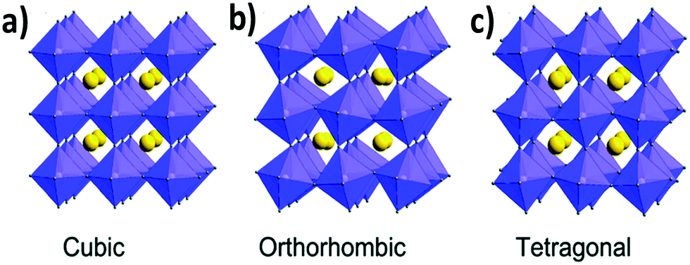 | ||
| Fig. 1 Different crystal structures of metal halide perovskites: (a) cubic, (b) orthorhombic and (c) tetragonal. Reproduced with permission.26 Copyright 2019, Royal Society of Chemistry. | ||
If the value of the tolerance factor is less than 0.8, then the size of cation A is too small to fit in the lattice. On the other hand, if t > 1.0, the size of cation A is too big to form a perfect perovskite structure. In that case, the concept of the formation of a hexagonal structure arises.16,22,23 Cubic crystal structures predominate for perovskite materials when the tolerance factor lies between 0.9 and 1.0. If t is 0.8–0.9 then orthorhombic, rhombohedral and tetragonal (Fig. 1b and c) perovskite crystals are more prone to form.
1.3. Advantages and disadvantages of halide perovskites
The power conversion efficiency of halide perovskites has increased enormously within the last few years. In 2009 the power conversion efficiency was 3.8%, which has increased up to 25% in recent years.24,25 Therefore, metal halide perovskites have gained intense attention as promising alternatives to conventional semiconductor materials for next generation optoelectronic applications with a facile synthesis process.26 In addition to solar cells,28 halide perovskites can be successfully applied to light emitting diodes (LEDs),27 photodetectors,29 lasers,30 field effect transistors (FETs),31 radiation detectors,32 encryption devices,33etc. Perovskite materials are now a hot topic in the optoelectronic field. The chemical stability of perovskites yet enables their outdoor application.34a Lead halide perovskites are susceptible to ready degradation in the presence of moisture, sunlight and UV radiation.34b,35 Degradation occurs in the following ways:36| CH3NH3PbI3(s) ↔ PbI2(s) + CH3NH3I(aq) |
| CH3NH3I(aq) ↔ CH3NH2(aq) + HI(aq) |
| 4HI(aq) + O2(g) ↔ 2I2(s) + 2H2O(l) |
| 2HI(aq) ↔ H2(g) + I2(s) |
Likewise, water reacts with metal hybrid perovskites to form ((CH3NH3)4PbX6·2H2O) which may weaken the hydrogen bonding interaction between the organic cation of the A site and the inorganic PbX6 octahedron of the B site. By this way, the crystal structure of the perovskite lattice changes.37 In this regard, MAPbBr3 is more stable than MAPbI3 as moisture can penetrate easily38 into MAPbI3 due to the difference of ionic radius (Table 1). MAPbI3 is prone to decompose more readily at a humidity of >55% compared to MAPbBr3 under the same conditions.38 Degradation in the presence of moisture, sunlight and oxygen causes a low efficiency39 of perovskites by the decrease of fluorescence intensity and photoluminescence quantum yields, which has poor impact on their photovoltaic application.
| Cation (A) | Effective radius (Å) | Ref. | Cation (B) | Effective radius (Å) | Ref. | Anion (X) | Effective radius (Å) | Ref. |
|---|---|---|---|---|---|---|---|---|
| Methylammonium [(CH3)NH3]+ | 2.17 | 23 | Pb2+ | 1.19 | 53 | Chloride (Cl−) | 1.81 | 55 |
| Formamidinium [CH(NH2)2]+ | 2.53 | 23 | Sn2+ | 1.10 | 54 | Bromide (Br−) | 1.96 | 55 |
| Cs+ | 1.88 | 53 | Sn4+ | 0.69 | 53 | Iodide (I−) | 2.20 | 55 |
| K+ | 1.64 | 53 | Ca2+ | 1.00 | 53 | |||
| Rb+ | 1.72 | 53 | Ge2+ | 0.73 | 53 | |||
| Mg2+ | 0.72 | 53 | ||||||
| Sr2+ | 1.18 | 53 | ||||||
| Ba2+ | 1.35 | 53 | ||||||
| Cu2+ | 0.73 | 53 | ||||||
| Fe2+ | 0.78 | 53 | ||||||
| Pd2+ | 0.86 | 53 | ||||||
| Bi3+ | 1.03 | 53 | ||||||
| Sb3+ | 0.76 | 53 | ||||||
| Ag+ | 1.29 | 53 |
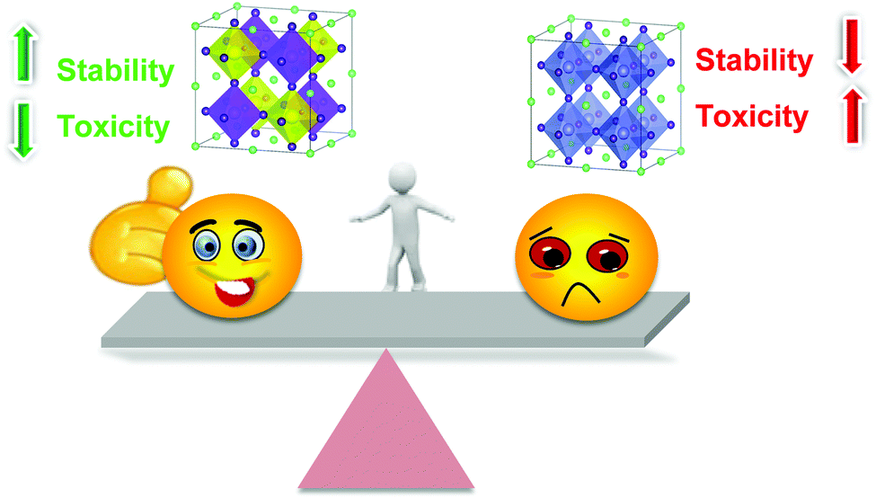
The toxicity of lead is another concern for the commercialization and large scale application of halide perovskites. Lead is a potent toxin for the environment and human body (Fig. 2).40a Even at a low exposure limit, it can cause severe damage to the nervous system and renal system, and also leads to impaired bone calcification.40b The ability of lead to replace the Ca2+ ion in protein kinase C enzyme affects the nervous system.41 Lead poisoning primarily arises by the ability of lead to form covalent bonds with the active site of the thiol group of many enzymes, which inhibits the activity of many antioxidant enzymes.42 Lead can easily contaminate environmental systems due to the water solubility of PbI2 (the Ksp value for PbI2 is 9.8 × 10⁻⁹ at 25 °C).43 This is the common problem for any toxic metal ion which is water soluble, mainly in polar solvents, and can be extracted into the environment easily through water.44 Lead can damage the ecosystems in the environment as well as in our body by this mechanism. In order to overcome these problems, researchers are trying to replace lead ions in the perovskite family with other homovalent and heterovalent cations, which results in more stable and less toxic perovskite materials. We will discuss this briefly in the next section.
 | ||
| Fig. 2 Exposure of the environment and children to lead. Reproduced with permission.40a Copyright 2018, Taylor & Francis. | ||
1.4. Formability of lead-free perovskites
Oxide perovskites have attracted considerable attention due to their excellent magnetic properties such as paramagnetism, ferromagnetism and magnetoresistance power.45–52 Halide perovskites have impressed the scientific community by their aforementioned properties (mentioned in Section 1.1) which are very interesting for potential photovoltaic application. However, the toxicity of lead and instability in the presence of moisture, sunlight and humid conditions are responsible for the non-commercialization and non industrialization of lead halide perovskite materials. Therefore, researchers are trying to find alternatives to lead based perovskites and develop lead-free halide perovskites for large scale application and capitalization. In Table 1 we summarise some commonly used metal ions in the lattice sites of A, B and X and their corresponding ionic radii which are important factors for the successful formation of perovskite materials.1.5. Design of lead-free perovskites
Regarding the toxicity of lead, replacement of lead ions with other homovalent metal cations56 having similar electronic configurations is a great approach. In this respect, tin and germanium can be potential alternatives as they belong from the same group in the periodic table. However, their poor stability in the divalent states hinders them from forming ideal 3D perovskite lattice structures. These materials are less stable as compared to their lead analogues. Due to the inert pair effect, the +2 states of tin and germanium are less stable than the corresponding +4 oxidation states, having a negative impact on their photovoltaic applications.57 A wide range of metal ions such as Ca, Pd, Cd, Hg, Ba, Be, Pt, Ni, Co, Zn, Mn, Fe, and Sr with stable divalent oxidation states can be considered as replacements for lead. However, all metal ions are not environmentally friendly (Cd, Hg) and suitable for photovoltaic application because of their high band gap (Be, Ca, Ba, Sr). Considering all the facts, Co, Ni, Mn, and Zn are the most promising candidates.58,59The heterovalent substitution of lead can give rise to 3D, 2D and 0D layered perovskites (Fig. 3b and c). Lead can be replaced by tetravalent metal cations (B4+) such as Sn4+ and Pd4+, leading to the formation of A2BX6 type perovskites.60a,b In addition to that, two trivalent metal cations (Bi3+, Sb3+) may also replace three lead ions to produce layered A3B2X9 compounds (Fig. 3b and d). Recently, research on double perovskites has gained tremendous importance due to their higher stability and non-toxic nature as compared to lead halide perovskites. The replacement of two divalent lead ions with heterovalent cations, i.e. one trivalent and one monovalent cations, leads to the formation of double perovskites. Double perovskites have the general formula of A2BB′X6 (Fig. 3a), where B is a monovalent cation (Ag+, Cu+) and B′ is a trivalent metal ion (Bi3+, In3+, Sb3+). Two toxic divalent lead ions are replaced by non-toxic monovalent (B) and trivalent (B′) metal ions in double perovskites which neutralize the overall charge in the perovskite lattice like conventional perovskites.60c–g Double perovskites are named so because their unit cell is double that of lead halide perovskites. Among all the possible structures of lead-free perovskites, double perovskites have come to the limelight due to their considerable stability and optoelectronic properties, which opens up a new avenue in the field of optoelectronic applications.
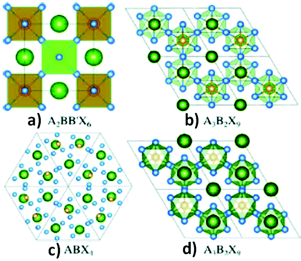 | ||
| Fig. 3 (a) Double perovskites, (b) 2-D perovskites, (c) 0-D perovskites and (d) polymorphs. Reproduced with permission.61 Copyright 2017, American Chemical Society. | ||
Unlike lead halide perovskites, very few review articles have been published on lead-free halide double perovskites about their synthesis, characterization and applications. Sargent et al. reported the development of the structures and stability of double perovskites.61 Liao et al. addressed the progress of lead-free perovskites.62 Tesfemichale et al. published an article which covered the electronic and optical properties of lead-free hybrid perovskites for optoelectronic applications.63 Inorganic layered and lead-free perovskites have been focused on for various photovoltaic applications such as LEDs, lasers, and solar cells.64 Nag et al. successfully highlighted the future aspects of Cs2AgBiX6 double perovskite nanocrystals.65 Numerous studies have been done to enhance the stability and tune the band gap.61 Recent theoretical and experimental approaches on the optical, electronic and defect properties of perovskite materials have been discussed in the report of Xiao et al..66 Fan et al. focused on the synthesis and properties of lead-free perovskite quantum dots.67
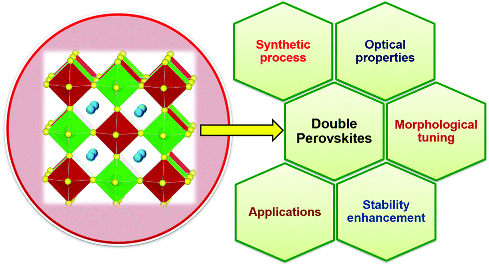
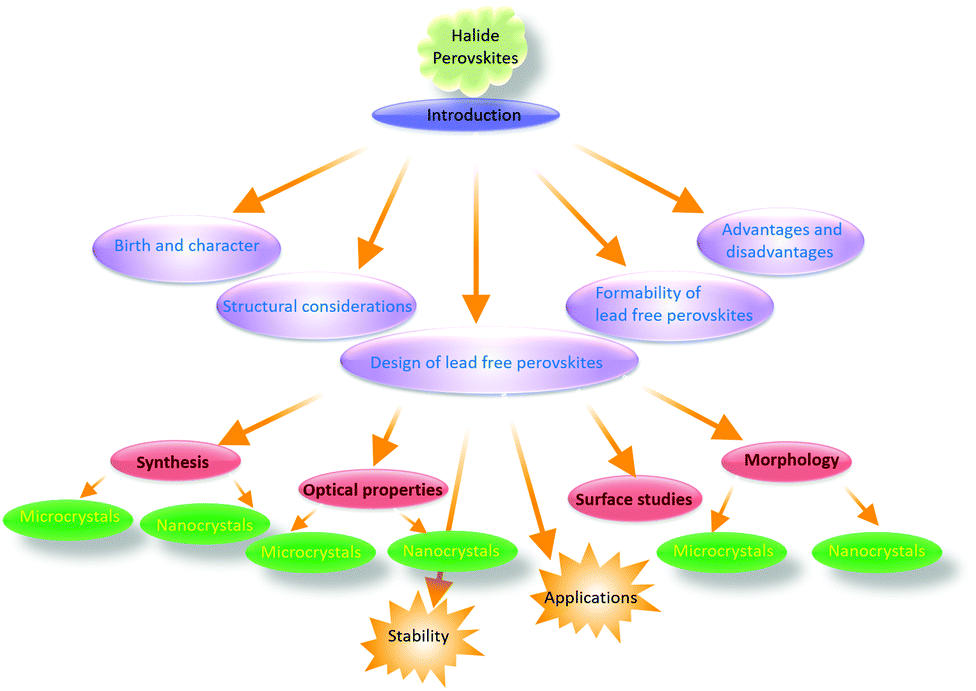
In this review, our aim is to present a complete picture of double perovskite (Scheme 1) materials which include both microcrystals and nanocrystals (Scheme 3). Earlier we discussed how double perovskite materials have gained importance (Scheme 2) and its significant factors. The probability for the formation of different structures of double perovskites was considered in the previous section. Later we are going to discuss deliberately the synthetic process of double perovskites. This review covers various optoelectronic properties of double perovskites. We have also aimed to discuss their different morphologies and stability. Finally, the optoelectronic application of double perovskites is investigated here. Among all the possible formations of double perovskite materials, Cs2AgBiX6 has been explored vastly. Besides it, Cs2AgInCl6, Cs2AgSbCl6, and Cs2CuSbCl6 have also gained attention due to their considerable properties.
 | ||
| Scheme 1 Schematic representation of lead-free double perovskites and distinct features of double perovskites discussed in the review. | ||
 | ||
| Scheme 2 Differences between lead-free double perovskites and lead halide perovskites. | ||
 | ||
| Scheme 3 Summary of the review. | ||
2. Material synthesis and crystal structures of halide double perovskites
Metal halide double perovskite materials like lead halide perovskites can be synthesized by a variety of ways such as spin coating, mechanochemical, anti-solvent reprecipitation, hot injection, and solvothermal methods.2.1. Synthesis and crystal structures of double perovskite microcrystals
Organic–inorganic hybrid double perovskites were first reported in 2016. The Anthony K. Cheetham group reported MA2KBiCl6.68 They first synthesized the starting material CH3NH3Cl by mixing CH3NH2 and HCl at 273 K temperature and then heating the mixture to 323 K for drying. MA2KBiCl6 was crystallized by mixing MACl, KCl and BiCl3 at 423 K in HCl medium by the hydrothermal technique. The resulting MA2KBiCl6 double perovskite crystallised in R![[3 with combining macron]](https://www.rsc.org/images/entities/char_0033_0304.gif) m symmetry. The authors compared the experimentally observed crystal structure with the density functional theory (DFT) model. The K–Cl bond length was slightly distorted and had a value of 3.049 Å. Bi–Cl had a bond distance of 2.681 Å. The K–Cl–Bi bridging angle was 173.04°. Wei et al. reported MA2AgBiBr6 3D cubic double perovskite,69 which crystallized in the Fmm space group having a lattice parameter of 11.64 Å. The Ag–Br and Bi–Br bond lengths were 2.95 and 2.87 Å respectively. Deng et al. reported MA2TiBiBr6 which is isoelectronic with MAPbBr3.70 This was also crystallized in a 3D cubic structure with the space group Fmm and had a lattice parameter of 11.76 Å. Yin et al. established theoretical calculation by the DFT model for synthesis of various chalcogenide double perovskites.71 The frozen-core projected augmented wave approach was used here including the core and electron applications. The authors identified nine chalcogenide double perovskites. These are Sr2SbTaS6, Ba2SbTaS6, Sr2BiNbS6, Ba2BiNbS6, Sr2BiTaS6, Ba2BiTaS6, Ba2SbTaS6, Ba2BiNbS6, and Ba2BiTaSe6. Slavney et al. reported a Cs2AgBiBr6 double perovskite single crystal.72 The large orange-red single crystal was synthesized from a concentrated HBr solution containing stoichiometric amounts of CsBr, AgBr and BiBr3. The single crystal showed a cubic face with space group Fmm having a unit cell of 11.25 Å. Cubic Cs2AgBiBr6 (Fig. 4a)73 with space group Fmm was also reported by the spin coating approach in 2018. CsBr, AgBr, and BiBr3 were mixed in a molar ratio of 2
m symmetry. The authors compared the experimentally observed crystal structure with the density functional theory (DFT) model. The K–Cl bond length was slightly distorted and had a value of 3.049 Å. Bi–Cl had a bond distance of 2.681 Å. The K–Cl–Bi bridging angle was 173.04°. Wei et al. reported MA2AgBiBr6 3D cubic double perovskite,69 which crystallized in the Fmm space group having a lattice parameter of 11.64 Å. The Ag–Br and Bi–Br bond lengths were 2.95 and 2.87 Å respectively. Deng et al. reported MA2TiBiBr6 which is isoelectronic with MAPbBr3.70 This was also crystallized in a 3D cubic structure with the space group Fmm and had a lattice parameter of 11.76 Å. Yin et al. established theoretical calculation by the DFT model for synthesis of various chalcogenide double perovskites.71 The frozen-core projected augmented wave approach was used here including the core and electron applications. The authors identified nine chalcogenide double perovskites. These are Sr2SbTaS6, Ba2SbTaS6, Sr2BiNbS6, Ba2BiNbS6, Sr2BiTaS6, Ba2BiTaS6, Ba2SbTaS6, Ba2BiNbS6, and Ba2BiTaSe6. Slavney et al. reported a Cs2AgBiBr6 double perovskite single crystal.72 The large orange-red single crystal was synthesized from a concentrated HBr solution containing stoichiometric amounts of CsBr, AgBr and BiBr3. The single crystal showed a cubic face with space group Fmm having a unit cell of 11.25 Å. Cubic Cs2AgBiBr6 (Fig. 4a)73 with space group Fmm was also reported by the spin coating approach in 2018. CsBr, AgBr, and BiBr3 were mixed in a molar ratio of 2![[thin space (1/6-em)]](https://www.rsc.org/images/entities/char_2009.gif) :1:1 in dimethyl sulfoxide to form a supersaturated solution. Before spin coating, both the precursor and substrate were preheated at 80 °C. Giustino et al. reported a series of lead-free double perovskite materials.74 DFT calculations for all the materials have been reported where Cs2AgBiCl6 double perovskite was synthesized only. Single phase Cs2AgBiCl6 was prepared by a solid state reaction procedure in a sealed fused silica ampoule. The starting materials CsCl, AgCl and BiCl3 were mixed in a ratio of 2:1:1 and were loaded into the sealed silica ampoule under a vacuum of 10−3 Torr. The mixture was heated to 500 °C for five hours and held at 500 °C for four hours. Finally, upon cooling to room temperature, a yellow polycrystalline product was obtained. The authors also performed structural refinement by the single crystal X-ray diffraction technique. Woodward et al. synthesized two lead-free double perovskites, Cs2AgBiCl6 and Cs2AgBiBr6.75 Double perovskites have been synthesized via both the solid state and solution phase synthetic procedures. Polycrystalline Cs2AgBiX6 was prepared from a mixture of HCl or HBr solution. H3PO2 and metal halide salts were also used during the synthesis. The collected precipitate was washed with ethanol and dried overnight. The authors also developed a way to synthesize Cs2AgBiX6 polycrystalline samples by mixing all the halide salts in a solid state synthesis process. All the reagents were ground for 20 minutes and then kept in a box furnace in air at 210 °C for 10 hours. It was found that two heating cycles were needed with grinding in between to obtain the phase pure products. All the compounds obtained from all of the synthetic routes showed similar X-ray diffraction (XRD) patterns. Double perovskites were crystallized in the cubic phase with space group Fmm. Our group recently reported an interesting phenomenon to synthesize Cs2AgBiX6 (X = Cl, Br) microcrystals in organic medium and a mixture of aqueous and organic media.76 All the halide salts were dissolved in DMSO to form the precursor. Then the precursor was injected into isopropanol to obtain the desired products in the organic medium. For the synthesis of materials in aqueous–organic media, we first dissolved bismuth halides in water in one pot and then concentrated acid was added to it to dissolve it completely. In another pot, cesium and silver halides were dissolved in DMSO and then all the halides were mixed together.
:1:1 in dimethyl sulfoxide to form a supersaturated solution. Before spin coating, both the precursor and substrate were preheated at 80 °C. Giustino et al. reported a series of lead-free double perovskite materials.74 DFT calculations for all the materials have been reported where Cs2AgBiCl6 double perovskite was synthesized only. Single phase Cs2AgBiCl6 was prepared by a solid state reaction procedure in a sealed fused silica ampoule. The starting materials CsCl, AgCl and BiCl3 were mixed in a ratio of 2:1:1 and were loaded into the sealed silica ampoule under a vacuum of 10−3 Torr. The mixture was heated to 500 °C for five hours and held at 500 °C for four hours. Finally, upon cooling to room temperature, a yellow polycrystalline product was obtained. The authors also performed structural refinement by the single crystal X-ray diffraction technique. Woodward et al. synthesized two lead-free double perovskites, Cs2AgBiCl6 and Cs2AgBiBr6.75 Double perovskites have been synthesized via both the solid state and solution phase synthetic procedures. Polycrystalline Cs2AgBiX6 was prepared from a mixture of HCl or HBr solution. H3PO2 and metal halide salts were also used during the synthesis. The collected precipitate was washed with ethanol and dried overnight. The authors also developed a way to synthesize Cs2AgBiX6 polycrystalline samples by mixing all the halide salts in a solid state synthesis process. All the reagents were ground for 20 minutes and then kept in a box furnace in air at 210 °C for 10 hours. It was found that two heating cycles were needed with grinding in between to obtain the phase pure products. All the compounds obtained from all of the synthetic routes showed similar X-ray diffraction (XRD) patterns. Double perovskites were crystallized in the cubic phase with space group Fmm. Our group recently reported an interesting phenomenon to synthesize Cs2AgBiX6 (X = Cl, Br) microcrystals in organic medium and a mixture of aqueous and organic media.76 All the halide salts were dissolved in DMSO to form the precursor. Then the precursor was injected into isopropanol to obtain the desired products in the organic medium. For the synthesis of materials in aqueous–organic media, we first dissolved bismuth halides in water in one pot and then concentrated acid was added to it to dissolve it completely. In another pot, cesium and silver halides were dissolved in DMSO and then all the halides were mixed together.
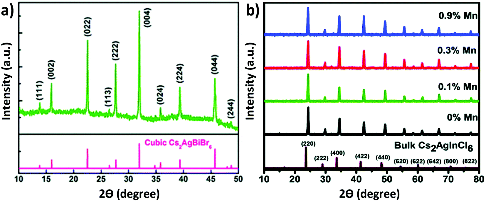 | ||
| Fig. 4 XRD pattern of (a) the Cs2AgBiBr6 thin film. Reproduced with permission.73 Copyright 2018, Royal Society of Chemistry. XRD patterns of (b) undoped and Mn doped Cs2AgInCl6 double perovskite MCs. Reproduced with permission.78 Copyright 2018, Royal Society of Chemistry. | ||
100 μL precursor was injected into the isopropanol followed by oleic acid to obtain the desired products. Both the reactions were carried out at 80 °C. We noticed that there was no change in the crystal structures of the microcrystals synthesized in the different media. All the materials were crystallized in their cubic face with space group Fmm. Angshuman Nag et al. reported the synthesis of Cs2AgInCl6 microcrystals and their corresponding Yb doped analogue.77 Microcrystals were synthesized from HCl medium by stoichiometrically mixing all halide salts. In order to synthesize the Yb doped double perovskites, the authors mixed YbCl3, InCl3 and AgCl in a sample vial containing HCl and heated the mixture at 75 °C under vigorous stirring. After 20 minutes, CsCl was added to the solution. Then the reaction mixture was filtered and the precipitate was dried at 110 °C in an oven. Nag et al. also reported Mn doped Cs2AgInCl6.78 Mn doped Cs2AgInCl6 was also synthesized by a similar procedure like Yb doped Cs2AgInCl6. All the undoped and doped compounds were crystallized in their cubic phase double perovskite with space group Fmm. It was noticed that there was no significant change in the crystal structure upon doping MnCl2 in the Cs2AgInCl6 double perovskite material (Fig. 4b). This was attributed to the small dopant concentration of MnCl2 in the parent perovskite. Crystal growth of Cs2AgInCl6 is also possible by the hydrothermal process.79 Liu et al. synthesized a Cs2AgInCl6 microcrystal by the hydrothermal method in a stainless steel Parr autoclave using 0.5 mL HCl, 2.4 mmol CsCl, 1.2 mmol AgCl and 1.2 mmol InCl3.79 They observed that white powder was obtained when the reaction was carried out at 423 K for 12 hours. At 423 K temperature, a large crystal was also formed by the continuation of the reaction for 72 hours. The product was filtered out and washed in ethanol and dried overnight for material characterization. The authors found that the Cs2AgInCl6 octahedral crystal formed by the alternation of AgCl6 and InCl6 in all three directions, which finally formed a 3D network. Synthesis of Cu doped double perovskites has a great impact on their optoelectronic properties.80a,b
Michaelis et al. synthesized Cs2AgSbCl6 and Cu doped Cs2AgSbCl6 double perovskites via solvent based synthesis.80a Here AgCl was prepared by mixing AgNO3 and HCl. At first 10 M HCl and H3PO2 were mixed and then heated to 120 °C. Then Sb2O3, AgCl and CsCl were added to it which finally formed a pale yellow colour precipitate. Cu doped analogues were synthesized using a similar process by the addition of different amounts of CuCl2 during the reaction. The XRD patterns showed that a face centred cubic double perovskite was formed with space group Fmm and a lattice parameter of 10.699 Å. The authors found that incorporation of Cu ions into the perovskite lattice resulted in a decrease of lattice parameter as the XRD plane shifted toward higher 2θ values (Fig. 5a) and the area (Fig. 5b) along with full width half maximum (FWHM) of the peak increased (Fig. 5c). This occurred due to the lower ionic radius of the dopant Cu2+ (0.87 Å) ion than those of Ag+ (1.29 Å) and Sb3+ (0.90 Å). Another antimony based lead-free Cs2CuSbX6 (X = Cl, Br) was proposed theoretically.74 George Volonakis reported Cs2AgInCl6 double perovskite81 by optimizing the structures of perovskite materials within the local density approximation (LDA) to DFT. A face centred cubic phase with an Fmm elpasolite unit cell was used as a structural template in that calculation. The atomic model consisted of InX6 and AgX6 octahedra which alternate along the (100), (010) and (001) directions. The obtained lattice constants for Cl, Br and I were 10.20 Å, 10.74 Å and 11.52 Å respectively. Volonakis et al. proposed that it is possible to synthesis Cl, Br and mixed Cl/Br analogues of Cs2AgInX6 experimentally and not the I derivative through the calculation of the tolerance factor and octahedral factor. However, Cs2AgInCl6 was synthesized by the solution based method at 110 °C using 10 M HCl, CsCl, AgCl, and InCl3 salts.
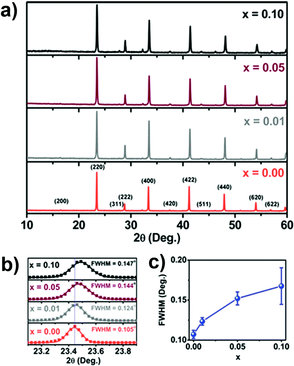 | ||
| Fig. 5 (a) XRD patterns of undoped and Cu doped Cs2AgSbCl6 MCs, (b) expansion of the (220) plane in the XRD patterns and (c) broadening of the FWHM. Reproduced with permission.80a Copyright 2018, American Chemical Society. | ||
2.2. Synthesis and crystal structures of double perovskite nanocrystals
Double perovskite nanocrystals can be synthesized by a variety of processes like double perovskite microcrystals.The Keli Han group synthesized Cs2AgBiX6 double perovskite nanocrystals by a solution based procedure.82 The authors dissolved all the halide salts in DMSO medium. Then they injected the precursor solution into an anti-solvent, isopropanol, in the presence of surface ligand oleic acid to form the desired nanocrystals. The nanocrystals were crystallized in the cubic phase with space group Fmm. Alivisatos et al. reported two lead-free double perovskite nanocrystals Cs2AgInCl6 and Cs2AgSbCl6.83 They developed a different synthetic process (Fig. 6a) for crystal growth. During the synthesis of Cs2AgInCl6 they used benzoyl chloride, whereas 2-ethyl-2-hexonyl chloride was used for the synthesis of Cs2AgSbCl6. Acetate salts of all metal ions were mixed in xylene at the time of synthesis of Cs2AgInCl6. Then oleic acid, oleylamine and benzoyl chloride were added to it and the reaction mixture was heated to 100 °C. After it, the resulting mixture was centrifuged and redispersed into hexane for material characterization. Acetate salts, oleic acid, oleylamine, xylene and 2-ethyl-2-hexonyl chloride were used for the synthesis of Cs2AgSbCl6via a hot injection method. Both the nanocrystals exhibited a cubic phase with the Fmm space group in the XRD pattern. The authors also carried out spin-polarized PBE-GGA based DFT for structural relaxation.
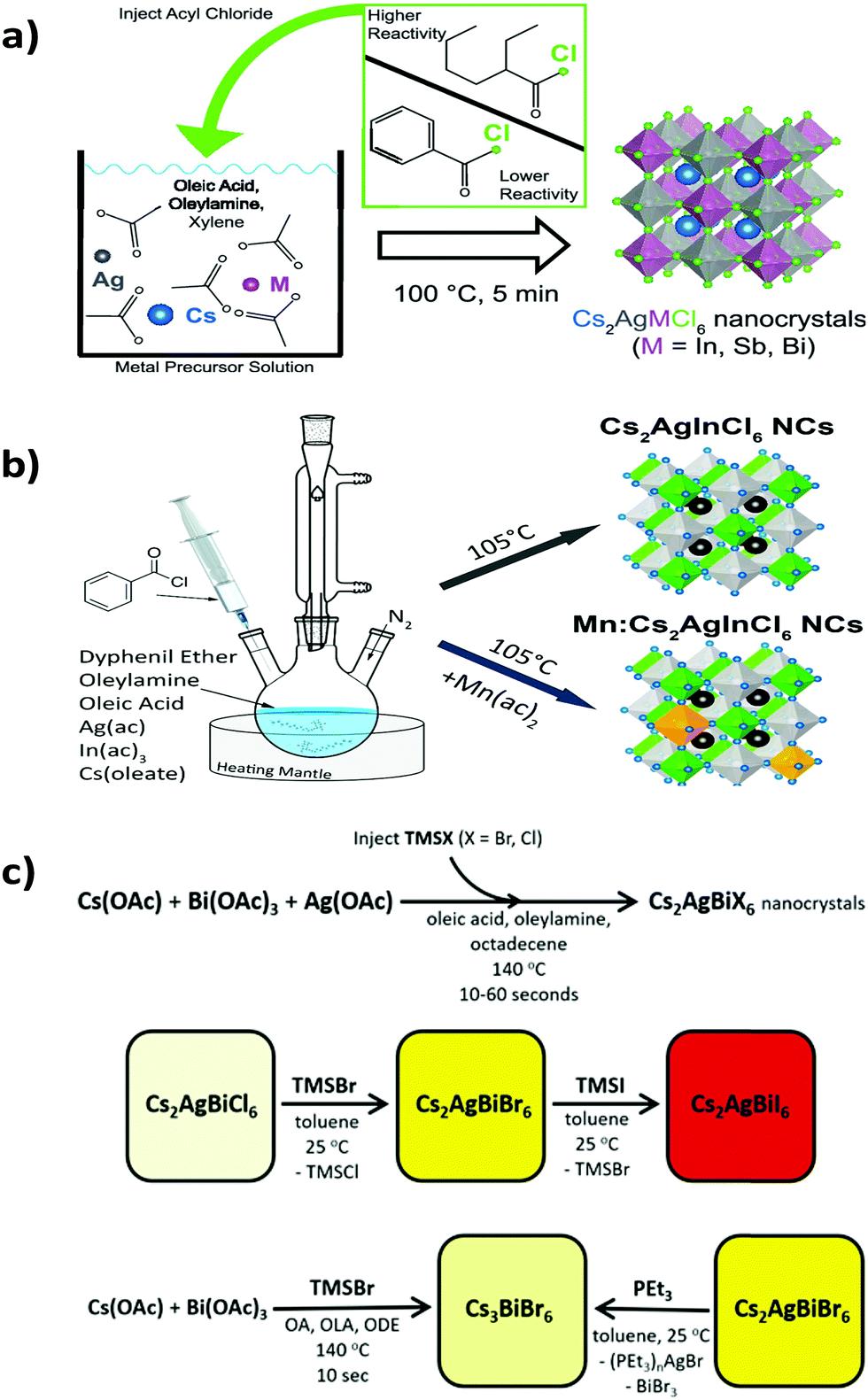 | ||
| Fig. 6 Synthesis of (a) metal halide double perovskite nanocrystals. Reproduced with permission.83 Copyright 2019, American Chemical Society. Synthesis of (b) undoped and Mn doped Cs2AgInCl6 nanocrystals. Reproduced with permission.84 Copyright 2018, American Chemical Society. (c) Cs2AgBiX6 nanocrystals via an anion exchange method. Reproduced with permission.86 Copyright 2018, American Chemical Society. | ||
Nag et al. reported Yb doped Cs2AgInCl6 double perovskite nanocrystals.77 Here also acetate salts of silver, indium and benzoyl chloride were used and the reaction was carried out via a hot injection method like the previously mentioned process. Nag et al. used cesium oleate as a precursor. Cesium oleate was prepared by mixing cesium carbonate and oleic acid at 140 °C and it was preheated to 100 °C before using in a reaction. A nitrate salt of Yb was used as a Yb precursor for doping Yb ions into the parent Cs2AgInCl6 nanocrystals. It was observed that due to the small dopant Yb concentration, there was no significant shift in 2θ value in the XRD peak positions. L. Manna et al. reported undoped and Mn doped Cs2AgInCl6 nanocrystals via a hot injection method.84 Silver acetate, indium acetate, cesium oleate, diphenyl ether (DPE), oleylamine and benzyl ether were used for the synthesis of nanocrystals (Fig. 6b). Mn was doped into the nanocrystals by using manganese acetate precursor. Keli Han et al. also reported the synthesis of Mn doped double perovskite nanocrystals.85 In this case the mother material was Cs2NaInxBi1−xCl6. The nanocrystals were synthesized by a variable temperature and one pot hot injection method. In the hot injection method, acetate salts of cesium, sodium, bismuth and indium were loaded into a mixture of oleic acid, oleylamine and octadecene, which was heated for 60 minutes under vacuum at 110 °C. Manganese acetate was added into the stirring reaction mixture to synthesise Mn doped nanocrystals. The nanocrystals revealed the cubic face centred structure with the Fmm space group in the X-ray diffraction pattern. There is a monotonic shift of diffraction peaks towards higher 2θ values in the powder XRD profile with the increase of the In/Bi ratio. This happens due to the smaller ionic radius of In3+ (94 ppm) than Bi3+ (117 ppm). Chlorine and bromine halide double perovskites have been explored vastly over iodine based double perovskites. Multiple computational studies have been done on the Cs2AgBiI6 double perovskite as a target of interest. However, experimentally it is difficult to synthesise due to its readily decomposable nature. Computational studies have been performed to investigate whether the material is thermodynamically stable with respect to its decomposition into another phase. In addition to that, Gamelin et al. reported an outstanding synthetic route for Cs2AgBiI6via a halide exchange procedure (Fig. 6c).86 Gamelin et al. synthesized Cs2AgBiX6 double perovskite nanocrystals by a hot injection method. They also reported that postsynthetic modification through anion exchange and cation extraction can give rise to Cs2AgBiI6, which is difficult to synthesise by any conventional process. Cesium acetate, silver acetate and bismuth acetate were mixed in octadecene, oleic acid and oleylamine to synthesize the nanocrystals. Then TMSCl was added to it to form Cs2AgBiCl6 nanocrystals. TMSCl was swiftly injected at 160 °C. Then centrifugation of the reaction mixture at 9000 rpm for 20 minutes followed by centrifugation at 10000 rpm and 6000 rpm by dissolving it in toluene and hexane, respectively, resulted in the formation of the desired nanocrystals, whereas addition of TMSBr formed Cs2AgBiBr6 nanocrystals. It was also demonstrated that the Br congener can be synthesized from the Cl congener by the addition of TMSBr to the Cs2AgBiCl6 nanocrystals. Similarly, addition of TMSI to the Cs2AgBiBr6 nanocrystals results in Cs2AgBiI6 double perovskite nanocrystals. Individually Cs2AgBiCl6 and Cs2AgInCl6 have gained attention in various synthetic approaches. In this respect, Bi doped Cs2AgInCl6 nanocrystals were also reported in the literature.87 Pristine and Bi doped Cs2AgInCl6 have been synthesized via a hot injection method. Powder XRD of these materials revealed the highly crystalline nature of the nanocrystals with space group Fm3m.
In Table 2 we summarize the various synthetic approaches with the respective space groups obtained from the XRD patterns for different lead-free double perovskite microcrystals (MCs) and nanocrystals (NCs).
| Material | Synthesis process | Space group | Ref. |
|---|---|---|---|
| MA2KBiCl6 MC | Hydrothermal |
Rm |
68 |
| MA2AgBiBr6 MC | Hydrothermal |
Fmm |
69 |
| MA2TiBiB6 MC | Hydrothermal |
Fmm |
70 |
| Sr2SbTaS6 MC | Theoretical DFT | P21/n | 71 |
| Sr2BiNbS6 MC | Theoretical DFT | P21/n | 71 |
| Sr2BiTaS6 MC | Theoretical DFT | P21/n | 71 |
| Ba2SbTaS6 MC | Theoretical DFT | P21/n | 71 |
| Ba2BiNbS6 MC | Theoretical DFT | P21/n | 71 |
| Ba2BiTaS6 MC | Theoretical DFT | P21/n | 71 |
| Ba2SbTaS6 MC | Theoretical DFT |
Rm |
71 |
| Ba2BiNbS6 MC | Theoretical DFT |
Rm |
71 |
| Ba2BiTaSe6 MC | Theoretical DFT |
Rm |
71 |
| Cs2AgBiBr6 single crystal | HBr solution |
Fmm |
71 |
| Cs2AgBiBr6 MC | Spin coating |
Fmm |
73 |
| Cs2AgBiCl6 MC | Solid state |
Fmm |
74 |
| Cs2AgBiBr6 MC | Both solid state and solution based |
Fmm |
75 |
| Cs2AgBiCl6 MC | Both solid state and solution based |
Fmm |
75 |
| Cs2AgBiX6 (X = Cl, Br) MC | Solution process |
Fmm |
76 |
| Cs2AgInCl6 MC | HCl solution |
Fmm |
77 |
| Cs2AgInCl6 MC doped with Yb | HCl solution |
Fmm |
77 |
| Cs2AgInCl6 MC doped with Mn | HCl solution |
Fmm |
78 |
| Cs2AgInCl6 | Hydrothermal | Fm3m | 79 |
| Cs2AgSbCl6 MC | HCl solution |
Fmm |
80a |
| Cs2AgSbCl6 doped with Cu | HCl solution |
Fm![[3 with combining overline]](https://www.rsc.org/images/entities/char_0033_0305.gif) m m |
80a |
| Cs2AgInCl6 MC | HCl solution |
Fmm |
81 |
| Cs2AgBiCl6 NC | Anti-solvent reprecipitation |
Fmm |
82 |
| Cs2AgBiBr6 NC | Anti-solvent reprecipitation |
Fmm |
82 |
| Cs2AgBiI6 NC | Anti-solvent reprecipitation |
Fmm |
82 |
| Cs2AgInCl6 NC | Hot injection |
Fmm |
83 |
| Cs2AgSbCl6 NC | Hot injection |
Fmm |
83 |
| Mn doped Cs2AgInCl6 NC | Hot injection |
Fmm |
84 |
| Cs2NaInxBi1−xCl6:Mn (0 ≤ x ≤ 1) | Hot injection |
Fmm |
85 |
| Cs2AgBiX6 NC | Hot injection |
Fmm |
86 |
| Bi doped Cs2AgInCl6 NC | Hot injection | Fm3m | 87 |
3. Optical properties
The optical properties of lead-free halide double perovskites are obtained from their visible light harvesting properties. The optical properties are investigated from several optoelectronic characterizations like band gaps, absorption coefficients, photoluminescence quantum yields, and lifetimes. The energy bandgap of a perovskite material is inversely proportional to the absorption threshold. Therefore, perovskites having higher bandgaps tend to exhibit narrow absorption. Generally, perovskite materials exhibit both direct and indirect bandgaps. The bandgap transition of lead halide perovskites appears mainly due to the ligand to metal charge transfer where the p-orbitals of halides predominate as the valence band maximum (VBM). Charge transfer occurs from the VBM to the conduction band minimum (CBM), which has lead p-orbital character in most of the cases. The electronic configuration of Pb2+ (6s26p0) allows the filled 6s orbital to mix effectively with the 5p orbital of the halide ion in the valence band, where the vacant lead 6p orbital acts as the conduction band.88 DFT calculation revealed that this composition of valence band maxima and conduction band minima contributes to the material's long carrier lifetime and shallow defect states, whereas the high p-orbital based density of states near the band edges is responsible for the strong absorption.89a,b3.1. Optical properties of double perovskite microcrystals
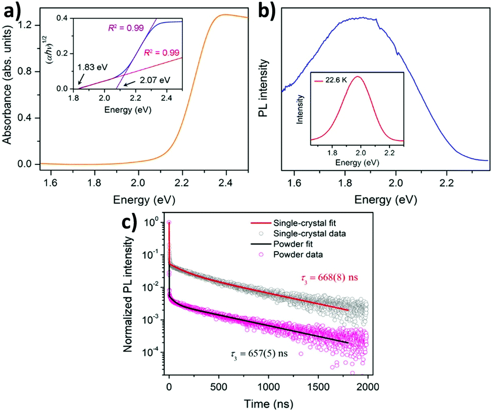
The metal hybrid MA2KBiCl6 double perovskite shows two edges in their reflectance spectrum.68 The Tauc plot determines the apparent optical bandgap value. The UV-visible spectrum exhibits two edges at 3.04 and 3.37 eV for the MA2KBiCl6 double perovskite. Yin et al. investigated the optical and electronic properties of chalcogenide double perovskites by calculating the band structures at PBE levels.71 Through the partial density of states, they established that antibonding coupling occurs between the Sb lone pair 5s and the S 3s at the VBM level similar to CH3NH3PbI3. They reported very low bandgaps for the materials. Although an indirect bandgap is not suitable for solar cell application because of the weak optical absorption at the band edge, the reported double perovskites have low bandgaps (ΔEg), facilitating easy electron–hole transport suitable for cell performance. So far we have discussed the optoelectronic properties of hybrid double perovskites. Now we will consider the optical properties of pure inorganic halide double perovskites.Karunadasa et al. reported a red orange double perovskite single crystal having a high life time.72 The material exhibits an indirect bandgap of 1.95 eV (Fig. 7a), which is very much suitable in a tandem solar cell for coupling with a Si absorber. The material has an indirect bandgap in the shallow absorption region beginning at 1.8 eV. This bandgap is slightly lower than the bandgap of MAPbBr3. At room temperature the material shows a weak photoluminescence (PL) peak centred at 1.87 eV, which indicates that it follows a non-radiative recombination pathway (Fig. 7b). Upon decreasing the temperature of the system, the PL intensity increases. At 23 K temperature the PL peak is more intense and blue shifted which is observed at 1.98 eV. The material shows a high lifetime of 660 ns (Fig. 7c). This does not vary significantly between the single crystal and powder sample. Therefore, this is the fundamental carrier lifetime of the material.
 | ||
| Fig. 7 (a) Absorption spectra, (b) PL spectra and (c) PL decay curves of Cs2AgBiBr6 double perovskite MCs respectively. Reproduced with permission.72 Copyright 2016, American Chemical Society. | ||
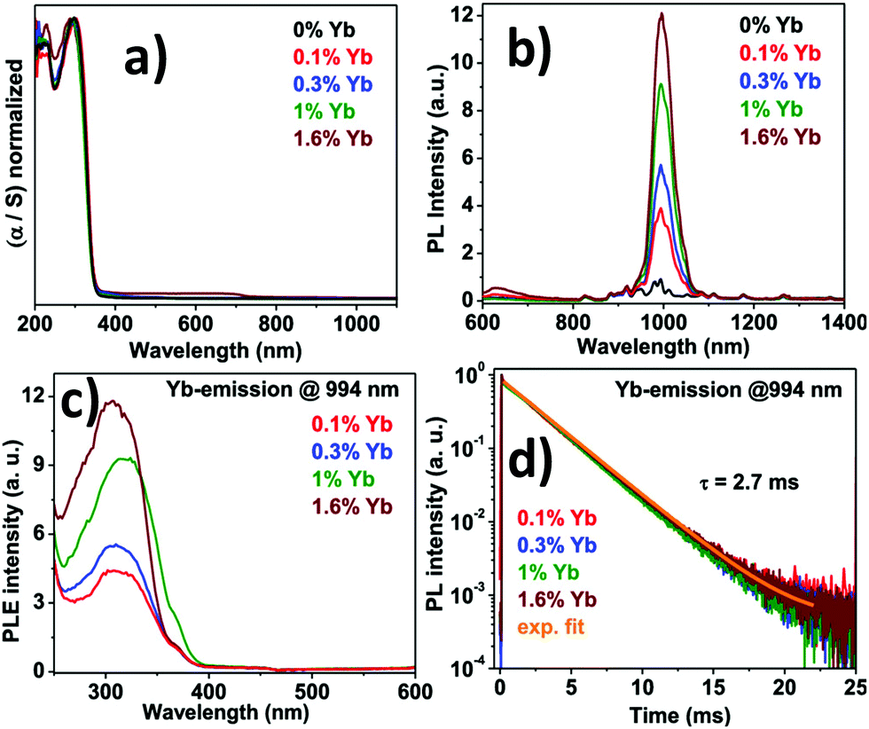
Guistino et al. calculated the bandgaps for a series of double perovskites which lie below 2.7 eV considered as indirect bandgaps.74 They reported that the band gap value increases randomly on moving up the halogens in the periodic table. This occurs due to the different characters of electronic states at the band edges. The Tauc plot of Cs2AgBiCl6 shows that the indirect band gap falls in the range of 2.3 to 2.5 eV. The material gives maximum emission at 575 nm or 2.2 eV which is red shifted from the absorption maximum. In addition to that, the time resolved photoluminescence decay curve fitted with the two exponential decay curve having a fast decay time of 15 ns and a slow decay period of 100 ns. The authors reported that the Cl-p and Ag-d characters are predominant in the electronic band structure and conduction band edges split into two bands due to spin–orbit coupling. McClure et al. reported Cs2AgBiCl6 and Cs2AgBiBr6 which have both direct and indirect bandgaps.75 The Woodward group reported that the onset of absorption spectra of double perovskites is not sharp as that of lead halide perovskites because of their indirect bandgaps.75 The band gaps of Cs2AgBiCl6 and Cs2AgBiBr6 were 2.77 and 2.17 eV respectively. The authors calculated the band value using the Kubelka–Munk equation, which expresses absorbance as a function of reflectance: F(R) = α = (1 − R)2/(2R). Here R is the reflectance and α is the optical absorption coefficient. Kar et al. established how the fluorescence intensity of double perovskites can be increased only by the addition of water. They reported that the fluorescence intensity of double perovskites gradually increases by the addition of water because the water molecule acts as a surface ligand along with oleic acid. Water, being a polar solvent, can dissolve the precursor salts more efficiently and increase the PL intensity and consequently the PLQY of the materials increases.76 Nag et al. reported near infra-red emission by doping Yb ions into Cs2AgInCl6 double perovskite microcrystals.77 All the microcrystals exhibit an absorption onset at 360 nm (Fig. 8a) of the direct band gap. The authors reported that due to the presence of low percentages of Yb ions in the perovskite hosts there is no shift in the absorption spectra. Yb ion doping results in NIR emission at 994 nm, which increases upon increasing the dopant concentration (Fig. 8b). PLE spectra (Fig. 8c) resemble UV spectra, which indicates that upon light excitation the host double perovskite transfers its excited energy to the dopant f electrons which undergo 2F5/2 → 2F7/2 electronic transition to produce NIR emission at 994 nm. PL decay dynamics reveals a single exponential curve (Fig. 8d) with a long material lifetime of 2.7 ms, which is also a characteristic of Yb3+ incorporation into the perovskite lattice. Nag et al. also reported the increase of fluorescence intensity by doping Mn ions into Cs2AgInCl6 double perovskite microcrystals.78 The absorbance value for each sample was 350 nm. An interesting change was observed in the emission wavelength from the undoped to Mn doped double perovskite. Undoped Cs2AgInCl6 exhibits weak emission at 619 nm, whereas doping with Mn ions produces strong emission centred at 632 nm with an FWHM of 300 meV. The Mn ion doped double perovskites have higher PLQYs up to 5% as compared to undoped samples. The transition of a Mn d electron from the 4T1 to 6A1 state is responsible for the increase of PL intensity after doping with Mn ions in the double perovskite. Mn doping also causes a significant increase of lifetime in the materials up to 974 μs. This high lifetime is accounted for by the spin forbidden transition of 4T1 to 6A1 of Mn d electrons in the Mn2+ doped Cs2AgInCl6 double perovskite.78 Liu et al. calculated the bandgap of Cs2AgInCl6 using the Kubelka–Munk function.79 The material consists of two distinct bands at 335 and 370 nm with a direct bandgap of 3.23 eV. Under 370 nm irradiation, the double perovskite exhibits broad red emission at 635 nm wavelength, which appears due to photo-induced defects in Cs2AgInCl6. The bi-exponential decay curve of the material has a slower decay lifetime of 16.3 μs and a longer decay period of 100 μs. With the help of excitation power dependent PL analysis, Liu et al. noticed that a well-defined PL peak is observed at 596 nm at 0.28 ms, which shifts towards a higher wavelength by increasing the delay time. This fact is attributed to the presence of filled subgap states at this timescale.
 | ||
| Fig. 8 (a) Absorption spectra, (b) PL spectra, (c) PLE spectra, and (d) PL decay dynamics of Yb doped Cs2AgInCl6 double perovskite MCs. Reproduced with permission.77 Copyright 2019, American Chemical Society. | ||
Michaleis et al. reported how the indirect bandgap of double perovskites can be reduced by doping with heterovalent metal ions.80a Doping Cu2+ ions into Cs2AgSbCl6 results in a dramatic shift in the optical bandgap of the double perovskite. The parent molecule shows an indirect bandgap of 2.65 eV in the diffuse reflectance spectrum, which decreases to 1.02 eV upon doping with Cu2+ ions in the double perovskite host. A drastic visual colour change is observed from yellow to black by doping with Cu ions. The reduction of the bandgap is further attributed to the absorption in the near IR region. Also, the band edge of the doped material is not sharp like the parent material due to the lattice disorders. Guistino et al. reported a direct bandgap Cs2AgInCl6 double perovskite semiconductor which turns from white to orange under UV light illumination due to photoinduced electronic or structural changes.81 This happens because of the strong sensitivity of the electronic structure of Cs2AgInCl6. The authors reported the square modulus of the electronic wave function at the band edges, which shows that the bottom of the conduction band is associated with the Cl-3p and In-5s/Ag-5s states, whereas the top of the valence band is comprised of the Cl-3p and In-4d/Ag-4d states. The material shows the first absorption maximum at 380 nm or 3.3 eV and the second absorption band at 585 nm or 2.1 eV. It exhibits a well-defined PL peak centred at 608 nm or 2.04 eV with an FWHM of 120 nm or 0.37 eV. The reported double perovskite exhibits a fast relaxation lifetime of 1ns and a slow decay time for a period of 6 μs. According to the literature, generally most of the Cs2AgBiX6 double perovskites fall in the indirect bandgap region, while Cs2AgInCl6 lies in the direct bandgap region. However, Bein et al. reported a direct bandgap Cs2AgBiBr6 double perovskite thin film. Absorption spectra of the material exhibit a peak around 550 nm wavelength, which corresponds to an Eg of 2.21 eV.89c A time-correlated single photon counting (TCSPC) study shows that the Cs2AgBiBr6 powder has a lifetime of 568 nm, whereas the film has a decay period of over 220 ns. The PL intensity of the Cs2AgBiBr6 powder is quenched approximately 60% on TiO2, while the reduction of intensity is observed more than 80% in the presence of spiro-OMeTAD. Until now, we have observed that several studies reveal a large number of Eg values, which mainly originate from different synthetic procedures along with the variable methods of measurement.
3.2. Optical properties of double perovskite nanocrystals
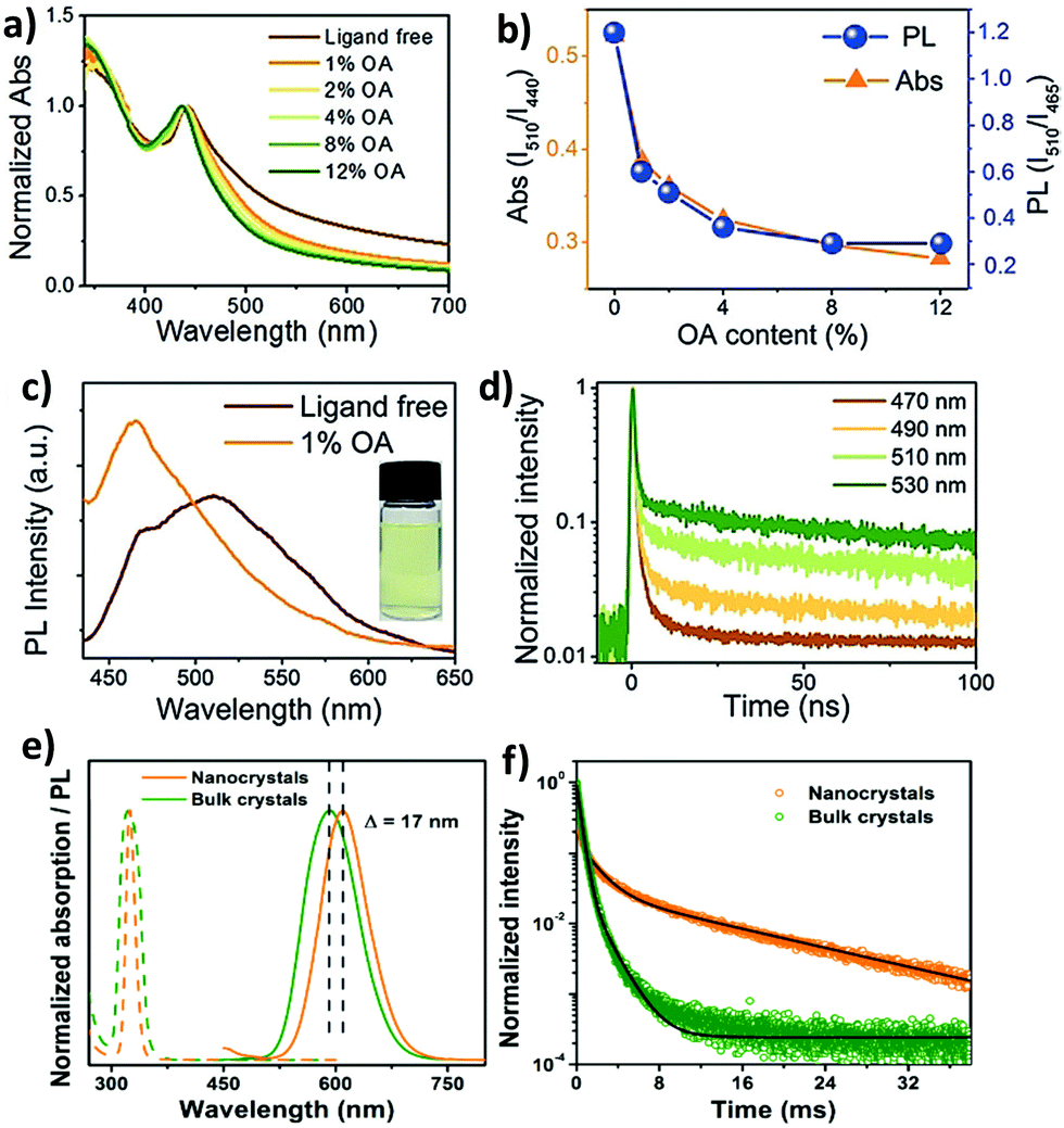
The optical properties of double perovskite nanocrystals are little bit different from the optical properties of double perovskite microcrystals. Let us discuss the similarities and differences between these two analogues of double perovskites.The bandgap reduction in double perovskite nanocrystals was reported by Zang et al. in 2020.80b Here Cu doping into Cs2AgInCl6 leads to the lowering of the bandgap in the double perovskite from 3.60 eV to 2.19 eV. Generally, the VBM of Cs2AgInCl6 is formed from the hybridization of Ag-4d and Cl-3p orbitals, whereas the CBM arises from the antibonding In-s orbital. Upon doping Cu2+ ions into the double perovskite, the Cu-3d orbital participates in the formation of the VBM and remains in the higher state than the Ag-4d orbital although the position of the CBM remains unchanged. Consequently, the bandgap value decreases. As a result of this, decreases in PL intensity and lifetime are observed. Han et al. reported Cs2AgBiX6 double perovskite nanocrystals which exhibit tunable emission in the range of 395 to 575 nm.82 They demonstrated a new phenomenon to increase the emission intensity of the perovskite nanocrystals by increasing the amount of oleic acid (OA) as a ligand during the formation of nanocrystals. Ligand free Cs2AgBiBr6 nanocrystals show an exciton peak at 440 nm wavelength (Fig. 9a). There is a long absorption tail up to 700 nm which appears due to the presence of sub-bandgap transitions caused by the existence of surface defects. These surface defects can be suppressed by the addition of surfactants such as oleic acid. Ligand free Cs2AgBiBr6 exhibits double emission peaks at 465 nm and 510 nm wavelengths (Fig. 9c). Upon increasing the content of oleic acid, the peak at 510 nm decreases, whereas the peak at 465 nm increases, which suggests that the emission peak that appears at 465 is due to band edge emission. Sub-band gap trap states are responsible for the 510 peak. The relative PL intensity (ratio of the PL intensity at the peak position of 510 nm to that of 465 nm) decreases like relative absorption (Fig. 9b). The PL intensity for all the halide nanocrystals was increased by the addition of an excess amount of oleic acid. The PLQY also increases with the increase of PL intensity due to the suppression of the non-radiative transition. The authors reported that Cs2AgBiBr6 exhibits maximum emission when 12% oleic acid is added, with the maximum PLQY of 0.7%, while Cs2AgBiCl6 exhibits the highest emission in the presence of 8% oleic acid. TCSPC measurement informs that the nanocrystals show tri-exponential decay where the long lived component is responsible in higher percentages at long PL wavelengths (Fig. 9d). When nanocrystals are synthesized in the presence of xylene and metal acetate, they exhibit interesting optical features.83 Cs2AgInCl6 nanocrystals have an absorption shoulder in the range of 290 to 310 nm wavelengths and band gaps of 4.15 ± 0.05 eV for diluted samples. Nanocrystals have broad emission at 567 nm due to the Laporte forbidden 4d → 5s transition at the band edges and a PLQY of 0.6%. On the other hand, Cs2AgSbCl6 nanocrystals show absorption at wavelengths of 360 and 300 nm. The Tauc plot shows that the nanocrystals have a band gap of 2.83 ± 0.02 eV. Cs2AgSbCl6 nanocrystals have weak emission at 300 nm due to the momentum forbidden transition because of the indirect band gap. Optical studies indicate that the nanocrystals have confinement energies of 0.7 eV for Cs2AgInCl6 and 0.3 eV for Cs2AgSbCl6 in the absorption spectra with Bohr exciton radii of 1.02 nm and 0.82 nm, respectively, for diluted nanocrystals. However, concentrated nanocrystals exhibit an indirect gap of 2.57 ± 0.05 eV for Cs2AgSbCl6 and a direct gap of 3.57 ± 0.03 eV for Cs2AgInCl6 like bulk samples. In general, double perovskites have low photoluminescence quantum yields, which can be increased by doping with heterovalent metal ions. We are going to discuss the various strategies briefly. For this purpose, Manna et al. reported doping of Mn ions into Cs2AgInCl6 double perovskite nanocrystals.84 The authors observed an absorption onset at 350 nm for both the undoped and doped nanocrystals corresponding to band gaps of 4.36–4.38 eV. Although the absorption spectra are similar in nature, the corresponding PL spectra differ from each other. Undoped nanocrystals have broad weak PL emission at 560 nm with a PLQY of 1.6 ± 1%, while Mn doped nanocrystals show strong bright orange emission at 620 nm with a PLQY value of 16 ± 4%. Mn doping produces 4T1 → 6A1 transition in the double perovskite host, which results in a shift of the broad emission from 560 nm to 620 nm. Time resolved (TR) PL analysis revealed microsecond long photoluminescence which is a characteristic of the spin forbidden nature of Mn2+ luminescence that occurs due to intersite energy-transfer between Mn centres. Homovalent metal ion (Yb3+ ion) doping into Cs2AgInCl6 can produce NIR emission which is very significant for optoelectronic applications.77 UV-visible spectra of undoped and Yb doped Cs2AgInCl6 have similar features and exciton absorption occurs at 345 nm. PL spectra of the samples reveal that the Yb doped double perovskite can produce emission in the NIR region, while the undoped sample shows weak emission only in the visible region at 607 nm. The f electrons of the dopant Yb ion cause NIR emission. Here transition occurs from 2F5/2 to 2F7/2 and PLQY increases. The PL decay curve informs that Yb doped nanocrystals show bi-exponential decay with a long life time of 3 ms and a comparatively short life time of 749 μs. Han et al. established how Mn doping can tune the PL spectra of inorganic halide double perovskite nanocrystals from yellow to bright orange red photoluminescence with a maximum quantum efficiency (PLQE) of 44.6%.85 Undoped Cs2NaInxBi1−xCl6 (0 < x < 1) nanocrystals show absorption and PL emission peaks at 324 nm and 424 nm wavelengths respectively. Undoped nanocrystals have a low PLQY, which increases upon doping with Mn ions. The PL peak of Mn doped nanocrystals shifts from 583 to 614 nm (Fig. 9e) due to the spin forbidden transition of Mn2+ ions involving 4T1 → 6A1 transition. Doping of Mn ions into the double perovskite nanocrystals results in an increase of emission wavelength as compared to the bulk, which is contradictory to the quantum confinement effect. The authors reported that the d–d transition of Mn2+ is responsible for this opposite observation. However, the PL lifetime also increases in the nanocrystals than the bulk materials (Fig. 9f). Gamelin et al. reported indirect bandgap perovskite nanocrystals.86 The absorption peaks for Cs2AgBiCl6 and Cs2AgBiBr6 nanocrystals occur at 3.39 and 2.87 eV respectively. Both the samples have weak broad orange photoluminescence with PLQYs of 0.3 ± 0.3%. Sometimes it is observed that the PL intensity of the double perovskite increases upon decreasing the temperature due to the decrease of trap states in the molecules.
 | ||
| Fig. 9 (a) Absorption spectra of ligand-free and OA capped Cs2AgBiBr6 NCs, (b) the variation of relative PL and relative absorption (ratio of the absorption at 510 nm to that at 440 nm), (c) PL spectra of ligand-free and 1% OA capped NCs (photograph of the colloidal ligand-free Cs2AgBiBr6 NCs), and (d) TR-PL kinetics of ligand-free Cs2AgBiBr6 NCs. Reproduced with permission.82 Copyright 2018, Wiley-VCH. (e) Steady-state absorption (dashed lines) and PL (continuous lines) spectra of Cs2NaIn0.75Bi0.25Cl6:Mn NCs (orange) and bulk crystals (olive green), and (f) TR-PL decay curves of Cs2NaIn0.75Bi0.25Cl6:Mn NCs (τavg = 8.7 ms) and bulk crystals (τavg = 0.6 ms). Reproduced with permission.85 Copyright 2020, American Chemical Society. | ||
The Gamelin group reported the same observation. They noticed that emission of the nanocrystals brightens at cryogenic temperature. At 20 K Cs2AgBiCl6 nanocrystals show a single broad emission band centred at 1.68 eV, while the Cs2AgBiBr6 spectrum has two emission bands, a broad band centred around 1.75 eV, and a more intense, narrower feature centred at 1.97 eV. It is confirmed through photoluminescence exciton spectra that the same species is responsible for the absorption and emission spectra for both the nanocrystals. The broad band in the nanocrystals appears mainly from defect or surface related states. As compared to bulk species, nanocrystals have more surface trapping states which are suppressed upon decreasing the temperature of the system and consequently increase the decay time of the luminescence. Therefore, Cs2AgBiBr6 nanocrystals show a decay time of <100 ns at 150 K temperature, which increases up to 1.4 μs at 82 K. On the other hand, homovalent doping on Cs2AgInCl6 can tune the emission spectra. The Aswani Yella group reported how Bi doping can tune the emission spectra from white to orange.87 The band gap decreases upon increasing the Bi dopant concentration and its nature changes from direct to indirect. Cs2AgInCl6 nanocrystals involve the formation of valence band maxima by the contribution of Ag 4d and Cl 3p orbitals, while the conduction band is constructed from the hybridization of Ag 5s, In 5s, and Cl 3p orbitals. In the case of the Bi based double perovskites, the VBM is formed by the hybridization of Ag 4d and Cl 3p orbitals and a conduction band maximum is formed with Bi 6p orbitals. The difference in character of the conduction band is responsible for the change in band gap nature on changing the ion involved in the formation of double perovskites. Therefore, Cs2AgInCl6 nanocrystals have a direct band gap of 3.46 eV and the Bi doped perovskite has a bandgap of 2.9 eV. This band transition occurs for the 30% or above 30% Bi doped double perovskite. However, except for the undoped nanocrystal, all Bi doped nanocrystals show an absorption maximum at 360 nm, which appears due to band edge absorption. The intensity of absorption increases upon increasing the dopant concentration. The authors excited all the compounds at 380 nm wavelength to record the fluorescence spectra. Nonemissive pure nanocrystals show white emission by doping with Bi ions. At low concentrations of Bi ions, the peak occurs in the range of 570 to 620 nm due to self-trap transition, which is attributed to the Jahn–Teller distortion of the [AgCl6] octahedron in the excited state. At high concentrations of Bi ions, the emission peak appears only at 420 nm due to band edge emission. In the case of the 15% and 30% Bi doped nanocrystals, both the band edge and sub-band gap defect level emissions occur. Nanocrystals have the highest lifetime of up to 17 ns for 60% Bi doped samples. However, it is clear from the above discussion that with the minimal change in the conduction band, the conduction band character can be tuned between s and p orbitals. In 2017, Tran et al. showed how to achieve a convergence of direct to indirect band gaps by the adjustment of conduction band maxima between s and p orbitals.90Fig. 10 clearly shows that the bandgap decreases when we go from direct to indirect bandgaps. Here the bandgap value decreases from In to Sb halides. Likewise, the Eg value decreases from indium to bismuth based perovskites.
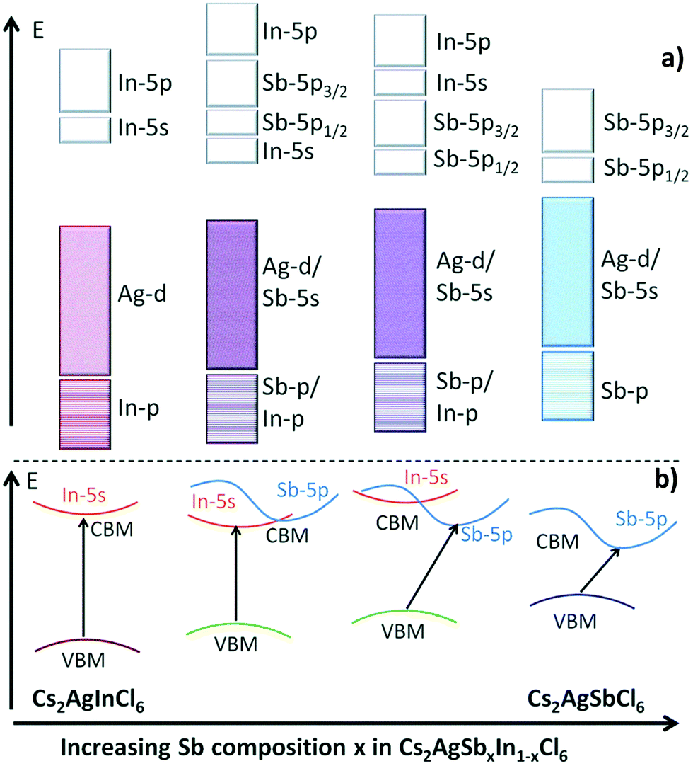 | ||
| Fig. 10 (a) Schematic diagram of the bonding and antibonding orbitals of Cs2AgSbxIn1−xCl6 and (b) transition from direct to indirect bandgaps on changing the character of the VBM and CBM. Reproduced with permission.90 Copyright 2017, Royal Society of Chemistry. | ||
4. Morphological studies
The morphologies of double perovskites have attracted the attention of researchers due to their interesting orientation, shape and size. The size and shape of double perovskites are highly dependent on the reaction process, i.e. the nature of the solvent used, the temperature of the system, and the heating or cooling rate. We will discuss thoroughly the morphologies of double perovskite microcrystals and nanocrystals in this section.4.1. Morphology of double perovskite microcrystals
Lei et al. reported a Cs2AgBiBr6 thin film.73 The film has a high coverage rough surface with an average grain size of 100 nm. There are undesired pinholes in the surface due to the restricted diffusivity of the precursor materials in the solvent drying stage at the time of spin-coating.Different morphologies of double perovskite microcrystals have been reported in the literature. However, tuning of the morphology of double perovskites is rare. Recently, Kar et al. invented an interesting way to tune the morphology of Cs2AgBiX6 (X = Cl, Br) double perovskite microcrystals.76 They observed that microcrystals are quasispherical in nature in organic medium. The morphology is tuned from quasi-spherical to quasi-octahedral on changing the reaction medium. This happens due to the presence of water molecules on the surfaces of the microcrystals which act as surface ligands along with oleic acid. Water molecules dissociate into hydroxyl ions and H3O+. Hydroxyl ions can replace oleate ions from the surfaces of the perovskite, which affects the growth of microcrystals and results in changes in shape and size of the microcrystals. Cs2AgBiCl6 changes its shape from quasi-spherical (Fig. 11a and b-HRTEM) to quasi-octahedron (Fig. 11c and d-HRTEM), while Cs2AgBiBr6 aggregates (Fig. 11e and f) itself. Nag et al. reported undoped and Yb doped Cs2AgInCl6 microcrystals in 2019.77 Growth of all the microcrystals occurs in multifaceted directions. The authors noticed that there is no change in shape and size of the double perovskite upon increasing the dopant concentration. Liu et al. reported Cs2AgInCl6 double perovskite microcrystals obtained by a solvothermal reaction process continued for 12 h.79 Microcrystals have a regular orthorhombic dodecahedral shape with an average size of 5 μm to 12 μm (Fig. 12a). The material has an fcc crystal with a tetrahedral crystallization habit which can form a truncated octahedral shape. The authors also determined the (111) and (100) planes from the facets of Cs2AgInCl6 microcrystals (Fig. 12b). They also reported 1.5 mm sized single crystals having a regular octahedral shape obtained by the hydrothermal reaction process continued for 72 hours (Fig. 12c and d). This observation suggests that the size of the single crystal can be changed by changing the reaction conditions. Pristine and Cu doped Cs2SbAgCl6 have been successfully reported in the literature.80a Here the morphology remained unchanged upon doping with heterovalent metal ions although the colour of the microcrystal changed (Fig. 12e). Micrometre sized polycrystals show microfaceted crystal growth (Fig. 12f).
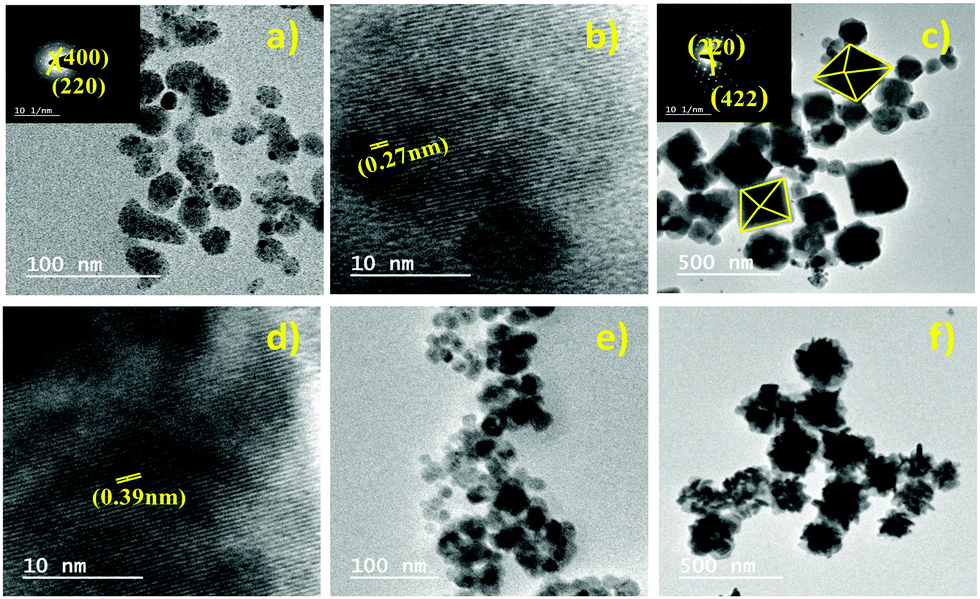 | ||
| Fig. 11 Cs2AgBiCl6 MCs: (a) TEM image (SAED pattern inset) and (b) HRTEM image in organic medium and (c) TEM image (SAED pattern inset) and (d) HRTEM image in aqueous medium. Cs2AgBiBr6 MCs: TEM images in (e) organic medium and (f) aqueous medium. Reproduced with permission.76 Copyright 2021, Elsevier. | ||
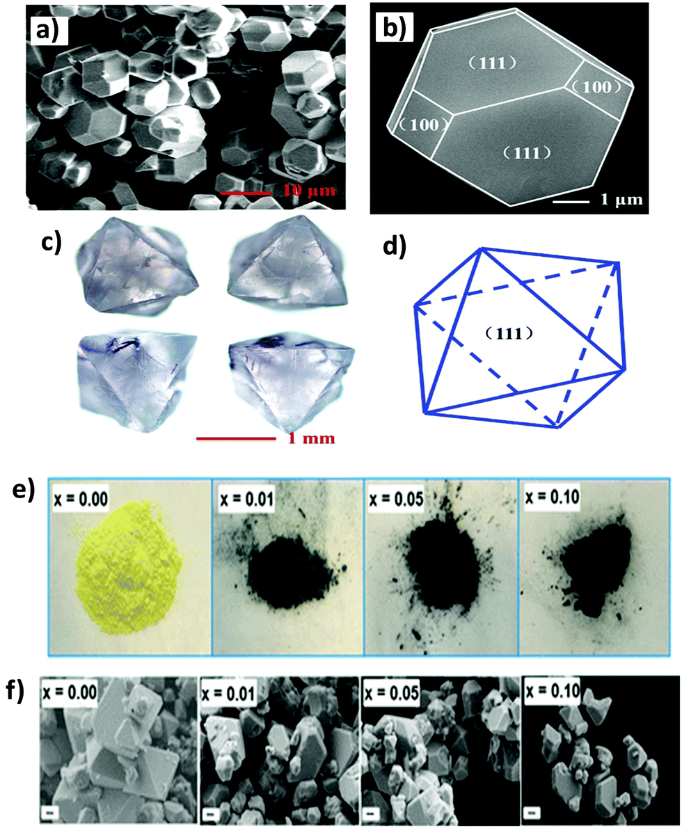 | ||
| Fig. 12 Cs2AgInCl6 MCs: (a) and (b) SEM images for 12 h reaction at different magnifications, (c) Cs2AgInCl6 single crystal for 72 h reaction and (d) simulated crystal faces for one crystal particle.79 Copyright 2017, Royal Society of Chemistry. Undoped and Cu2+ doped Cs2SbAgCl6 MCs: (e) photographs and (f) FESEM images of polycrystalline materials, where x is the nominal Cu2+ loading. Reproduced with permission.80a Copyright 2018, American Chemical Society. | ||
4.2. Morphology of double perovskite nanocrystals
The morphology of nanocrystals is somewhat different from that of microcrystals. The morphology of microcrystals is generally analysed by scanning electron microscopy (SEM), whereas transmission electron microscopy (TEM) is used to investigate the shape and size of double perovskite nanocrystals.Cs2AgBiBr6 nanocrystals which were synthesized in 2018 by a solution based procedure had a quasispherical shape with an average size diameter of 5.0 nm and a size distribution of 1.0 nm. These nanocrystals were highly crystalline in nature.82
Manna et al. reported undoped and Mn doped Cs2AgInCl6 double perovskite nanocrystals (Fig. 13).84 Pristine nanocrystals consisted of 9.8 nm cubic shaped particles. Although there is no change in the shape of nanocrystals upon doping with Mn ions, their size increases to some extent. Mn doped nanocrystals are 11–12 nm in size with uniform distribution of Mn ions throughout the lattice of the double perovskite.
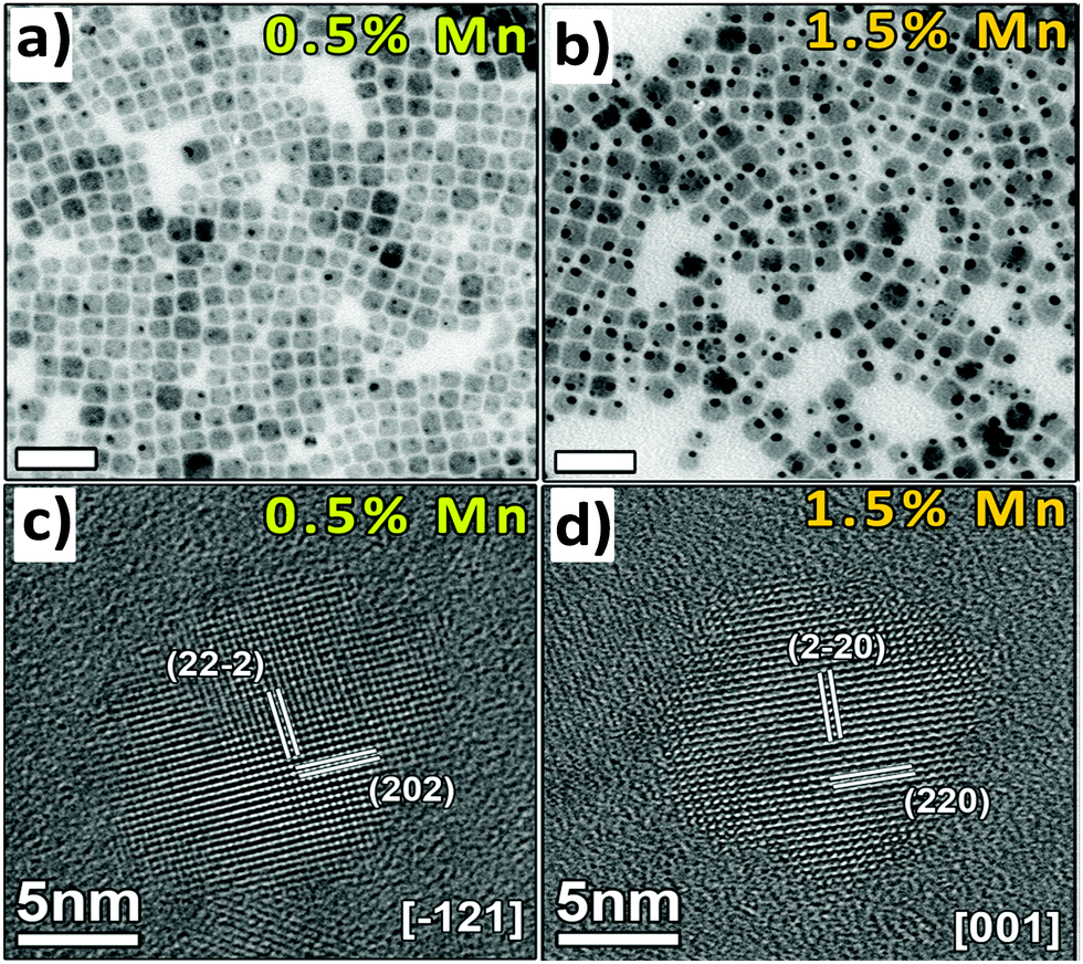 | ||
| Fig. 13 TEM images of (a) 0.5% and (b) 1.5% and HRTEM images of (c) 0.5% and (d) 1.5% Mn-doped Cs2AgInCl6 NCs respectively. Reproduced with permission.84 Copyright 2018, American Chemical Society. | ||
According to the literature it has been observed that most of the double perovskite nanocrystals are formed with a cubic shape. Similarly, undoped and Mn doped Cs2NaInxBi1−xCl6 nanocrystals have a cubic shape with an edge length of 10.59 nm and a mean size of 10.93 ± 0.9 nm.85 The Gamelin group reported how the size of nanocrystals can be tuned by the variation of solvent from which nanocrystals are precipitated or extracted.86 They synthesized the nanocrystals by a hot injection method. After successful synthesis and centrifugation, when the particles were extracted from toluene, it was observed that the resulting particles were in cubic shape with an edge length of 8 nm and had narrow size distribution. On the other hand, when nanoparticles were extracted and precipitated from hexane, the obtained particles had relatively broad size distribution with an average edge length of 13 nm. Therefore, the particle size, shape and distribution of double perovskites can be successfully tuned by the change of solvent during the synthesis of materials.
Yella et al. reported Bi doped Cs2AgInCl6 double perovskite nanocrystals. Pure Cs2AgInCl6 has a cubic shape which changes upon increasing the concentration of Bi dopant (Fig. 14a–o).87 For different contents of Bi ions, nanocrystals have different shapes such as cubic particles, a mixture of cubic and pentagonal particles, and hexagonal-shaped particles. When 30% Bi was doped, the nanocrystals again remained in cubic shape. The SAED pattern of the materials show the highly crystalline nature of the nanocrystals. The authors also compared the TEM and XRD analysis and they found that all the double perovskite nanocrystals were formed from the pure cubic phase with no traces of impurities. So far we have discussed how the size of the double perovskite can be changed by changing the solvent. Now we will focus on the influence of temperature during the synthesis and its effect on the size of the double perovskite. Wu et al. demonstrated the role and consequence of postannealing in/on the surface morphology and crystallinity of Cs2AgBiBr6 perovskite thin films.91 SEM and AFM images show that the grain size and crystallinity of the perovskite increase gradually with the increase of the temperature of the post-annealing process (Fig. 14p–y). Due to solid state dewetting (preferential diffusion of the component away from grain boundaries), the roughness of the film increases upon increasing the post-annealing temperature. Without annealing, the as-prepared film has a grain size of 50 nm with an average size of 38 nm, which increases after post-annealing. The average size is 50 nm at 150 °C, which changes to 410 nm at 300 °C. Therefore, the grain diameter changes from the nanosize to microsize by the annealing process due to the structural reconstruction of the double perovskite.
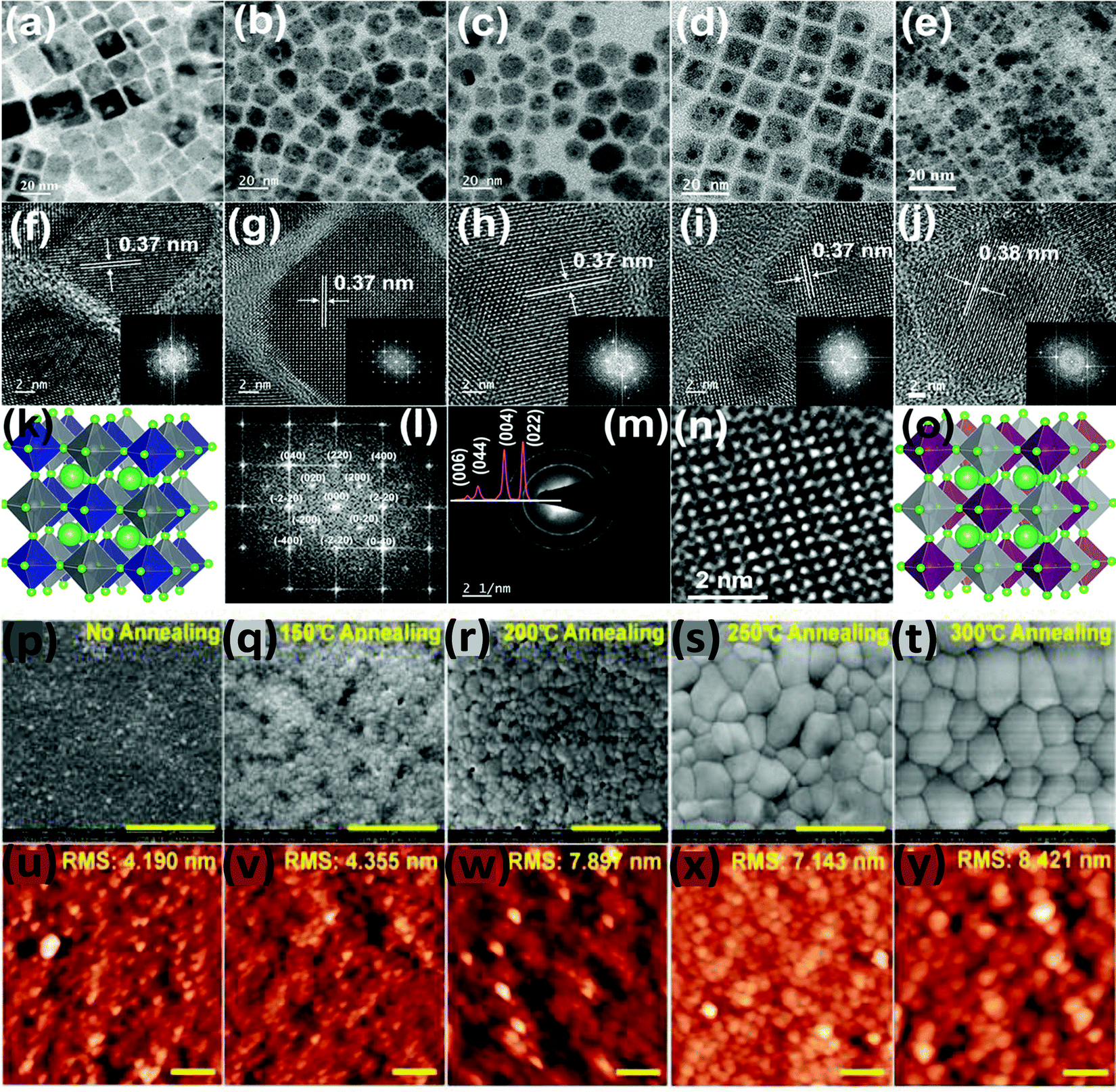 | ||
| Fig. 14 TEM images of Cs2AgIn1−xBixCl6 at different doping concentrations of Bi: (a) 0% Bi, (b) 5% Bi, (c) 15% Bi, (d) 30% Bi, and (e) 100% Bi; the corresponding HRTEM images and FFT spectra (f–j); simulated FFT and SAED patterns of 5% Bi (l and m); crystal structures of Cs2AgInCl6 and Cs2AgBiCl6 (k and o); and atomic resolution of the 30% Bi-doped nanocrystals (n). Reproduced with permission.87 Copyright 2019, American Chemical Society. Cs2AgBiBr6 films annealed at different temperatures: (p–t) SEM and (u–y) AFM. Reproduced with permission.91 Copyright 2018, Wiley-VCH. | ||
5. Stability
Hybrid lead halide perovskites are unstable under atmospheric conditions. They are prone to degrade in the presence of heat, water, and sunlight and easily convert back to their corresponding precursor materials. Inorganic halide perovskites (CsPbBr3) are more stable than methyl ammonium halide perovskites. However, they suffer from the toxicity issue due to the presence of toxic lead cations. In addition to all the facts, double perovskites are more stable because of their moisture and heat resistance capability. However, when we think about the stability of halide double perovskites, a lot of factors such as thermodynamic stability, mechanical stability, chemical stability, and device stability need to be considered. Halides play an important role in the thermodynamics of double perovskites. Down the group, i.e. from Cl to I, the thermodynamic stability decreases.92,93 In this section we will discuss the stability of double perovskite materials in different media and under various conditions.5.1. Stability of double perovskite microcrystals
Inorganic halide double perovskites show good stability because of their inorganic counterions. Slavney et al. compared the stability of Cs2AgBiBr6 crystals with MAPbBr3.72 They exposed the synthesized material to light and moisture and noticed changes in P-XRD under different conditions. It was reported that there was small surface decolourization for some of the irradiated samples after 15 days due to the sensitivity of silver to the light which recovered its original colour upon storing the samples in ambient light for 2 days. No decomposition of the overall material was observed after exposing it to sunlight and humidity. Similarly, degradation in light due to the presence of silver ions has been reported in many articles for Cs2AgBiCl6,75 Cs2AgSbCl6,94etc. The crystals of Cs2AgBiBr6 were stable up to 430 °C and no phase transition within this temperature was observed. This kind of highly thermally stable material is very useful for solar cell applications.72 Several groups have reported the chemical and thermal stability of Cs2AgBiCl6 and Cs2AgBiBr6. However, Cs2AgBiI6 is unstable60,95 like MAPbI3 due to the negative impact of I− ions96 in the decomposition process. Therefore, it is very hard to synthesise iodide based double perovskites unlike their chloride and bromide analogues. Liu et al. reported the chemical as well as light and thermal stability of Cs2AgInCl6 double perovskite microcrystals by exposing them to light and moisture, and the stability was confirmed by performing P-XRD in 7, 14 and 26 day intervals (Fig. 15a).79 The authors found no change in thermal and chemical stability with respect to the crystal size although there is evolution of the AgCl impurities in XRD spectra upon increasing the exposure time. Along with the crystal stability, the thermal stability of the perovskite is very important for optoelectronic applications. According to the literature, the material is relatively stable up to 400 °C (Fig. 15b). A small hump at 200 °C occurs because of some water molecules absorbed in the surface of the perovskite. A major change occurs from 400 to 615 °C with a weight loss of 42.64 wt%. In the DSC curve, an exothermic peak occurs at 539 °C due to the evaporation of CsAgCl2. The decomposition process of Cs2AgInCl6 can be thought of in the following way:| Cs2AgInCl6 → CsAgCl2 + CsInCl4 |
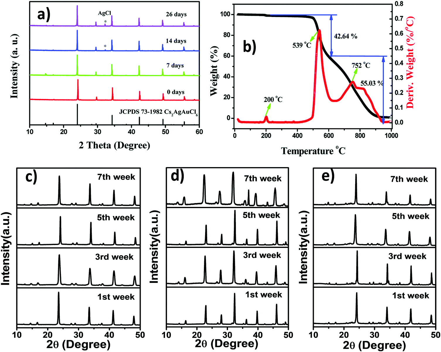 | ||
| Fig. 15 Cs2AgInCl6 MCs: (a) P-XRD patterns at 7, 14 and 26 day intervals, and (b) TGA and DSC curves. Reproduced with permission.79 Copyright 2017, Royal Society of Chemistry. P-XRD patterns of (c) Cs2AgBiCl6 MCs and (d) Cs2AgBiBr6 MCs in organic medium, and (e) Cs2AgBiBr6 MCs in a mixture of aqueous and organic media. Reproduced with permission.76 Copyright 2021, Elsevier. | ||
CsInCl4 can further be dissociated into CsCl and InCl3. AgCl and CsCl evaporate around 752 °C. This is the third weight loss in the DSC curve which is observed in between 650 and 1000 °C. Our group recently disclosed that double perovskite microcrystals prepared in organic medium were stable up to two months (Fig. 15c and d).76 It was also noticed that the materials were simultaneously stable beyond months when the materials were synthesized in a mixture of aqueous and organic media (Fig. 15e). We stored the synthesized microcrystals in the laboratory under ambient conditions and checked their crystal stability by performing P-XRD every week. No decomposition peaks for any starting material or impurities were found in the XRD spectra.
This observation indicates that, unlike lead halide perovskites, double perovskites are simultaneously stable in organic medium as well as a mixture of aqueous and organic media, which is helpful for optoelectronic applications. Michaelis et al. observed the long-term stability of the Cs2AgSbCl6 double perovskite in an outstanding way.80a They examined both the moisture and thermal stability of the double perovskite in different atmospheres for the parent and Cu2+ doped Cs2AgSbCl6 double perovskite microcrystals. The polycrystalline undoped and 10% Cu doped materials were stable up to 365 and 30 days, respectively, under 55% relative humidity. There was no decomposition peak in the absorption, NMR and P-XRD spectra (Fig. 16a and b). The thermal stability determined by a TGA experiment revealed that the polycrystalline undoped material was stable up to 250 °C (Fig. 16c).
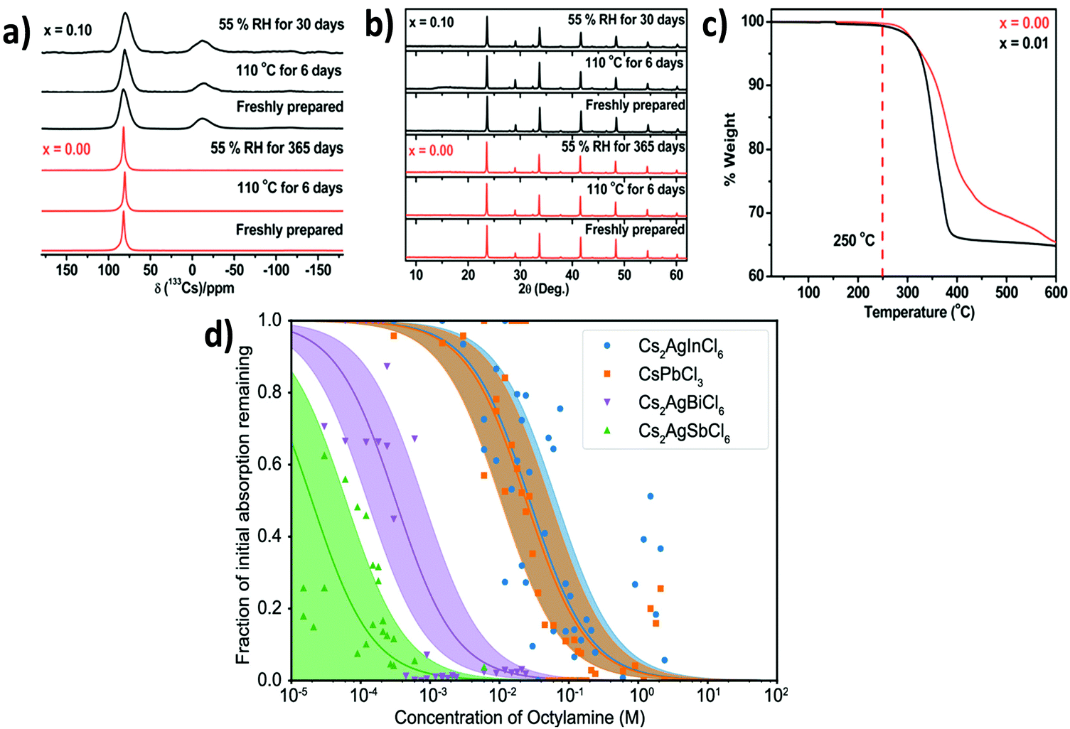 | ||
| Fig. 16 (a) NMR, (b) P-XRD and (c) TGA spectra of undoped and Cu doped Cs2AgSbCl6 MCs. Reproduced with permission.80a Copyright 2018, American Chemical Society. (d) Stability analysis of Cs2AgSbCl6, Cs2AgInCl6, Cs2AgBiCl6 and CsPbCl3 NCs by amine titration. Reproduced with permission.83 Copyright 2019, American Chemical Society. | ||
The compound is stable even after heating at 110 °C for 6 days. So it can be stated that these compounds show high optical and structural stability in every aspect. Cs2AgBiBr6 double perovskite can maintain its crystal phase purity for several months. However, the material degrades easily by alloying with another metal ion such as Tl due to the mixing of ionic and covalent bonding.97 Halide double perovskite based devices are stable up to several months or weeks. Ning et al. demonstrated that Cs2AgBiBr6 based solar cells are stable over 25 days under both dark and ambient conditions.98 A Cs2AgBiBr6 perovskite solar cell was reported to be stable for four months under ambient conditions.99 Double perovskite based devices have the capacity to retain their stability under continuous illumination under ambient conditions.98,99 Double perovskites used for X-ray detectors also show good stability under ambient conditions without any encapsulation.100
5.2. Stability of double perovskite nanocrystals
The variation of solvent can affect the stability of double perovskite nanocrystals by different ways. Perovskite nanocrystals can decompose rapidly in highly polar solvents like N,N-dimethyl formamide and acetone due to their tendency to dissolve ion type perovskites.101Protonic isobutanol can ease the proton exchange between oleic acid and oleylamine used for the synthesis of nanocrystals and results in a dynamic equilibrium between surface bound and free ligands.102 By this way, isobutanol can impart more stability to the nanocrystals as compared to acetone. Due to the low polarities and dielectric constants of chloroform and octane, the nanocrystals are stable in these solvents for several weeks. Zhou et al. proclaimed the stability of Cs2AgBiBr6 nanocrystals under moisture, high temperature, 55% relative humidity and dark conditions.103 There was no peak of the decomposition material in the XRD spectrum after storing the perovskite for 90 days. The compound is also sustainable at 100 °C in a dry N2 atmosphere for 300 hours and constant illumination (700 mW cm−2) for 500 hours. These results validate that the nanocrystals are very much tolerant to the heat, moisture and light, which is very meaningful for a wide range of optoelectronic applications. Aliviasto et al. demonstrate the quantitative stability of perovskite nanocrystals by a comparison method through titration assay where Cs2AgSbCl6, Cs2AgInCl6, Cs2AgBiCl6 and CsPbCl3 NCs were titrated with amines based on the decomposition reaction of halide perovskites with the amines (Fig. 16d).83 Double perovskites undergo reaction with amines in the following way:
| Cs2AgMCl6 + RNH2 ↔ MCl3RNH2 + Cs2AgCl3 |
In addition to the structural measurement, the stability of perovskites can also be checked by the optical and morphological studies. Sometimes alloying results in lower stability of double perovskites. Chen et al. reported that Mn and Yb doping on double perovskite nanocrystals could change the photoluminescence of the materials,104 whereas their stability remained unchanged. All the samples were stable up to three weeks and this was confirmed by structural, optical and morphological studies (Fig. 17).
 | ||
| Fig. 17 Stability (optical, structural and morphological) of Yb and Mn doped nanocrystals: (a, e and i) normalized absorption spectra, (b, f and j) normalized PL intensity, (c, g and k) XRD spectra, and (d, h and l) TEM images respectively. Reproduced with permission.104 Copyright 2019, American Chemical Society. | ||
6. Application of double perovskites
Lead-free double perovskites have not been explored vastly in respect of their application as compared to lead halide perovskites because a lot of research is ongoing to understand the structural and fundamental photo-physical properties of these materials properly. In spite of these obstacles, they have attracted excellent research attention in various optoelectronic applications.Cs2AgBiBr6 single crystals can be successfully applied for solar cells due to their indirect bandgap of 1.95 eV, which is suitable for coupling with a Si absorber in a tandem solar cell.72 Single crystals of Cs2AgBiBr6 can be applied for detectors with high responsivity and detectivity, which are comparable with those of MAPbX3 perovskites.
Wu et al. reported an inverted planar heterojunction perovskite solar cell based on Cs2AgBiBr6 double perovskite with a power conversion efficiency of 2.23%.91 The authors measured the PL quenching effect of Cs2AgBiBr6 films on Cu–NiO and C60, which results in prominent decreases of PL intensity, indicating charge transfer from the perovskite film to the charge exciton layers. It was also reported in the literature that the performance of films enhances as the grain size and crystallinity of the films increase with increasing temperature. A hysteresis-free highest power conversion efficiency of 2.23% is achieved with VOC = 1.01 V, JSC = 3.19 mA cm−2, and FF = 69.2% during the forward scan and a power conversion efficiency of 2.21% results with VOC = 1.00 V, JSC = 3.23 mA cm−2, and FF = 68.4% during the reverse scan (Fig. 18a–d). This value is lower than the theoretical calculation value of 7.92%. This difference may occur for thick double perovskite films.
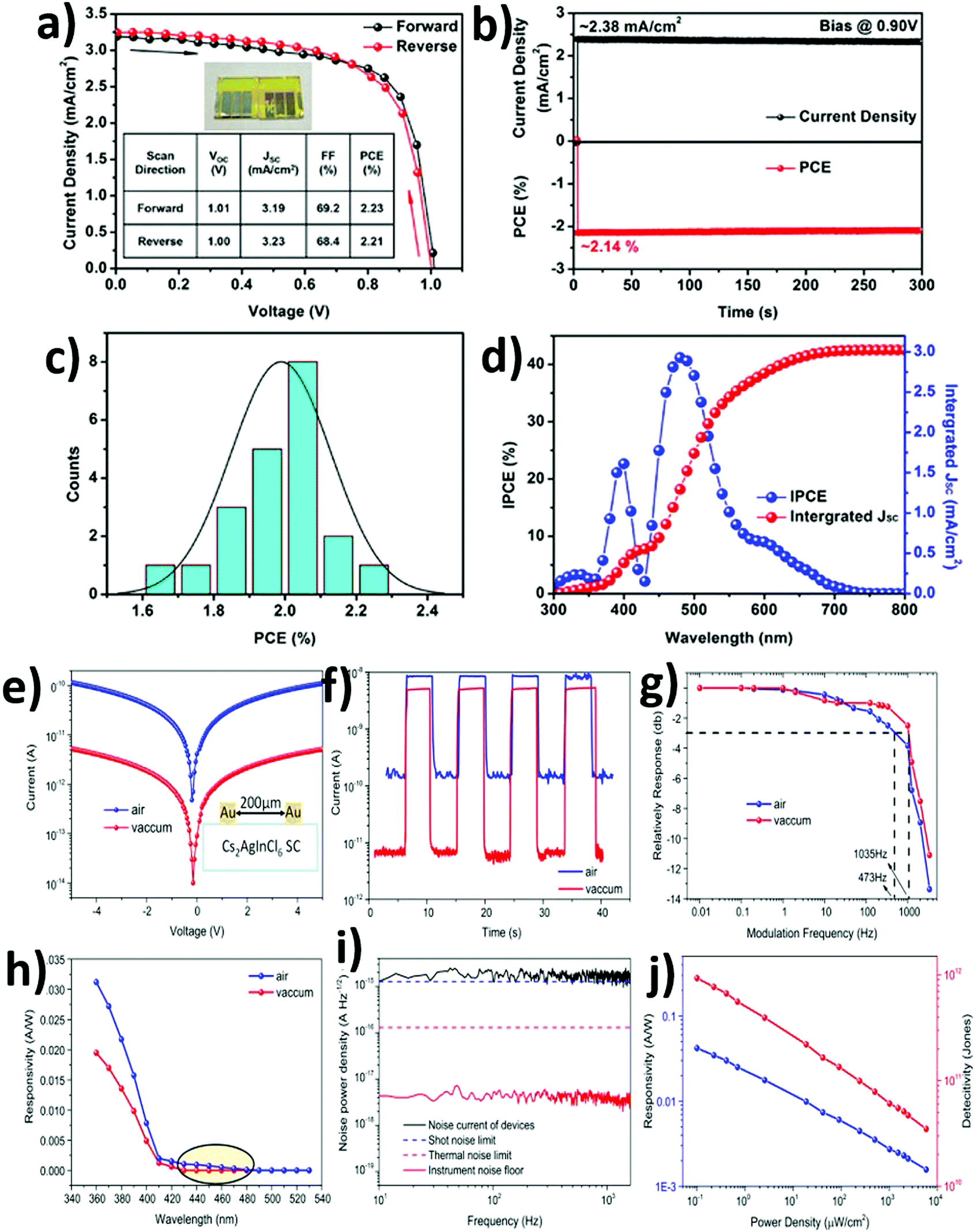 | ||
| Fig. 18 (a) Forward and reverse scans of J–V curves, (b) stabilized power output together with current density, (c) statistics of the PCE distribution, and (d) IPCE spectra. Reproduced with permission.91 Copyright 2018, Wiley-VCH. Photoelectric performances of Cs2AgInCl6 single crystals: (e) current–voltage characteristics under dark conditions, (f) light to dark current voltage curves, (g) normalized response of the detector, (h) wavelength dependent responsivity, (i) measured dark-current noise, and (j) light-intensity dependent responsivity. Reproduced with permission.105 Copyright 2018, American Chemical Society. | ||
A Cs2AgInCl6 single crystal was used as a visible-blind UV detector (Fig. 18e–j).105 The authors performed all the experiments in air and under vacuum to show the effect of oxygen on the device performance. Moreover, Cs2AgBiCl6 and Cs2AgBiBr6 have been employed as thermoelectric materials. Use of double perovskites in different aspects has been reported by many groups. Solar energy can be stored in a photochemical cell of the Cs2AgBiBr6 double perovskite.106 Here methyl glycogen and cobalt complexes of [cobaltII/IIItris(bipyridine)] were used and their redox potential was calculated using cyclic voltammetry. At a current density of 0.1 mA cm−2, the charging voltage in the dark was found to be around 1.8 V, which was higher than the potential difference of the coupled cell (E(MV+/MV2+) – E(Co2+/Co3+)). This could be due to the higher overpotential required for the conversion of MV2+ to MV+ and Co2+ to Co3+ or the resistance of ion transfer across the cell membrane. A Cs2AgBiBr6 thin film can also be used as a photodetector.107 In order to make the thin film as a photodetector, it was fabricated as a coplanar metal–semiconductor–metal inter-digitated pattern Au electrode configuration. This configuration was like a Au/Cs2AgBiBr6/Au structure, which facilitated the processes of generation, transfer, and collection of photogenerated carriers. When the energy of the incident light became larger than the semiconductor bandgap, then the film absorbed photons and produced a large number of electron–hole pairs due to the photoelectric effect. These photogenerated carriers rapidly separated and were attracted to the opposite electrode under an external electric field. The photocurrent increases with electric field intensity as the amount of photogenerated carriers is directly proportional to the absorbed photon flux, which follows the law of I = m·Pμ, where m is a proportional constant for a certain wavelength, P is the illumination power of the incident light, and μ represents the response of photocurrent to the given light intensity. The photodetector has higher photoresponsivity, which is measured in terms of the photocurrent generated by the per unit power of incident light for per unit area for a small device area or low light power. Several groups have focused on understanding the nature and working principles of double perovskites on photovoltaic devices. Bartesaghi et al. studied the charge dynamics of Cs2AgBiBr6 using photoinduced time resolved conductance measurement. The film of the double perovskite exhibited a charge carrier mobility of >1 cm2 V−1 s−1.108 Pan et al. measured the charge carrier mobility of Cs2AgBiBr6 single crystals employing a space charge limited current method and the value was 11.81 cm2 V−1 s−1.
Luo et al.103 reported Na alloyed Cs2AgInCl6 double perovskite which results in warm white light for indoor lighting.109 The device was fabricated by pressing the Na alloyed Cs2AgInCl6 powder into a commercial ultra-violet chip, without any silica encapsulation for protection. The CIE coordinates of the warm white light were (0.396, 0.448) at a colour temperature of 4054 K. There was very negligible degradation for a white LED under operating conditions of 5000 cd m−2 for over 1000 h in air, which indicates a promising application for white phosphor.
Single crystals of double perovskites can also be used for X-ray detectors. Yuan et al. synthesized a Cs2AgBiBr6 single crystal and applied this crystal for the detection of X-rays (Fig. 19).110 They used phenyl ethylamine bromide which is capable of regulating the order–disorder phase transition into the single crystal and results in the improvement of the ordering extent of alternatively situated [AgX6]5− and [BiX6]3− octahedra. By this process, the defect density and self-trap excitation are suppressed, the band gap is tuned and the carrier mobility is enhanced. Consequently, these make the double perovskite single crystal a potential candidate for X-ray detector application. The photoconductive device made for X-ray detection had an Au/Cs2AgBiBr6/Au structure with an electrode area of 2 mm2. Photoconductive gain (M) could be calculated by the M = Tc/Td equation, where Tc represents the carrier lifetime and Td is the carrier transit time. Td is equal to d2/μU, where d and μ are the carrier transit length and carrier mobility, respectively, and U represents the bias voltage. The authors reported that the μT product values for pristine Cs2AgBiBr6 single crystals and PEA-Cs2AgBiBr6 were 9.14 × 10⁻⁴ cm2 V−1 s−1 and 1.94 × 10⁻³ cm2 V−1 s−1 respectively. Thus PEA-Cs2AgBiBr6 shows better detection performance compared to the pristine one.
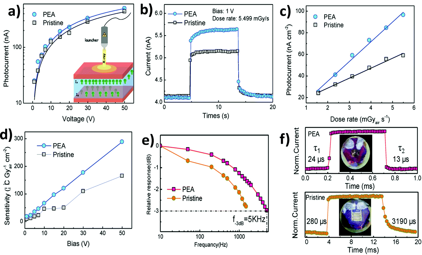 | ||
| Fig. 19 (a) I–V curves of Cs2AgBiBr6 and PEA-CS2AgBiBr6 single crystal detectors, (b) device response to X-rays, (c) photocurrent intensity as a function of X-ray source, (d) sensitivity under different biases of the X-ray detector, (e) normalized response of the detector to output signal frequency, and (f) photocurrent response of pristine and PEA-Cs2AgBiBr6 single crystal detectors. Reproduced with permission.110 Copyright 2019, Wiley-VCH. | ||
In addition to that, lead-free 2D hybrid halide double perovskites have also been explored for X-ray detection.111,112 Sun et al. reported (BA)2CsAgBiBr7 and (chloropropylammonium)4AgBiBr8 double perovskites which are highly effective for X-ray detection.111 The presence of organic cations offers a high mobility lifetime including the low density of traps and defects, and high bulk resistivity, which makes these hybrid lead-free 2D double perovskites promising components for X-ray detection. Simultaneously, iodide a halide-based (4,4-difluoropiperidinium)4AgBiI8 perovskite was studied to investigate its magnetic properties and X-ray detection capacity.112 Moreover, a lead-free 2D hybrid double perovskite was reported as strong polarization sensitive materials.113 The alteration of organic–inorganic sheets in (i-PA)2CsAgBiBr7 results in a quantum-confined bilayered structure of 2D archetype which shows high anisotropy in terms of physical properties that include optical absorption and electrical properties. This anisotropic nature of the 2D hybrid double perovskite results in a strong polarization-sensitive response.
Weng et al. reported a Cs2AgBiBr6 perovskite microcrystal as a humidity sensor and it was operated in the humidity range of 15% to 78% at 25 °C.114 The device was prepared by the anti-solvent drop casting method on a silica substrate where the precursor halides were dissolved in DMSO, and methyl benzene was used as an anti-solvent.
The response and recovery times of the Cs2AgBiBr6 thin film were 1.78 and 0.45 s respectively. The high recovery time of the thin film results from the plane structure of the film, from where water molecules can be easily volatilized during the desorption process.
Zhou et al. reported photocatalytic CO2 reduction by Cs2AgBiBr6 perovskite nanocrystals where the electron consumption was 105 μmol g−1 under AM 1.5G illumination for 6 h (Fig. 20).103 Upon constant irradiation for 6 hours the unwashed nanocrystal is able to evaluate CO (R(CO)) and CH4 (R(CH4)) with the quantity of 5.5 and 0.65 μmol g−1 respectively without any H2 evolution. The ethanol washed nanocrystal evaluate R(CO) and R(CH4) with the quantity of 14.1 and 9.6 μmol g−1 respectively which is 6.5 fold more than the unwashed nanocrystals. In this contrast, Xu et al. reported successful application of Cs2AgBiBr6 nanocrystals for photocatalytic dye degradation for Rhodamine B (RhB), Rhodamine 110 (Rh110), methyl red (MR), and methyl orange (MO) under visible-light irradiation (λ > 420 nm).115 In the case of Rhodamine B dye, the degradation process needs 12 hours for completion. The overall photodegradation process goes through the superoxide radical reaction and follows zeroth order kinetics. Other dyes degrade very slowly as compared to Rhodamine B dye because the surface of RhB is negatively charged, which facilitates the adsorption of positive charged RhB dye more effectively in comparison with neutral or anionic molecules like MO and MR.
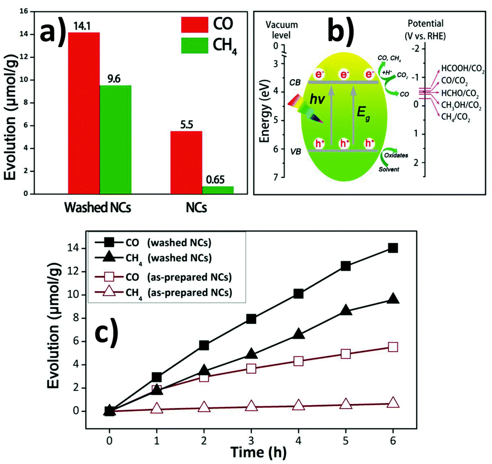 | ||
| Fig. 20 (a) Comparison of the performance of CO2 reduction between the as-prepared and washed Cs2AgBiBr6 nanocrystals, (b) photo-reduction of CO2 on the surfaces of the nanocrystals, and (c) time courses of CO and CH4 evolution. Reproduced with permission.103 Copyright 2018, Wiley-VCH. | ||
7. Limitations of double perovskites
Lead-free halide double perovskites have attracted excellent research attention due to their high stability and tunable absorption-emission in the whole UV and visible regions. In this contrast, double perovskites have some limitations for which they experience a few obstacles for a large scale commercial application in the field of optoelectronic devices. Now we will discuss these factors.A. One of the most important drawbacks of double perovskites is their low photoluminescence quantum yields. Several groups have focused on increasing the PLQY of double perovskites. Sometimes doping with another metal ion or adding water during synthesis may result in an increase in the PLQY of double perovskites to some extent by suppressing the surface defect.
B. Usually double perovskites have a stable cubic structure. However, the cubic unit cell sometimes restricts the orbital interaction which leads to a narrow conduction band and a large bandgap.
C. Preparation of double perovskites needs high temperature which causes difficulty to some extent in device fabrication.
D. Usually, PL spectra of double perovskites are broad in nature which consist of large FWHM values. Therefore, it is difficult to obtain color purity in the CIE coordinates.
E. In order to understand the charge transfer process, charge carrier dynamics should be investigated more deeply.
F. Dimensional reduction of double perovskites may help in overcoming the problems of electronic structures and results in bandgap transition.
G. The morphology (size and shape) of halide perovskites could be tuned easily.It is difficult to tune the morphology of double perovskite easily.
H. We have to precisely control the amounts of starting materials during the formation of double perovskites. In addition to that, component engineering could be possible by doping with rare earth elements, which may cause a significant change in optical properties.
In spite of all the obstacles, double perovskites have gained considerable research interest recently and have established themselves as promising alternatives to lead halide perovskites. Beyond solar cell application, double perovskites can be successfully implemented in sensors, photocatalysis, LEDs, photodetectors, X-ray detectors, etc.
8. Summary and outlook of the review
In this review, we have gone through a complete survey of double perovskite microcrystals and nanocrystals. Here, we have discussed how double perovskites can be synthesized in a variety of ways. This review has demonstrated that, depending on the methodology of reaction processes, the optical properties of double perovskites change, which is established by several photo-physical techniques. It has been noticed through morphological evolution that double perovskites have different shapes in nano- as well as microphases. Double perovskites have gained importance over lead based perovskites due to their high stability. We have explained different factors responsible for the high stability of double perovskites. Moreover, different applications of double perovskites have been vastly explored here. Simultaneously, all the merits and demerits of double perovskites have been discussed here. Therefore, we hope that this review will present a clear understanding about various properties of double perovskites and attract a broad readership.Conflicts of interest
The authors declare no conflict of interest.Acknowledgements
P. K. sincerely thanks the Science and Engineering Research Board (CRG/2020/000702), India. S. G. thanks MoE, India, for her doctoral fellowship. H. S. thanks UGC, India, for his doctoral fellowship.References
- Z. A. Borgschulte and L. Sachlapbach, Hydrogen as a Future Energy Carrier, Wiley-VCH Verlag GmbH & Co., 2008, ISBN: 978-3-527-30817-0 Search PubMed.
- J. R. Petit, Nature, 1999, 399, 429–436 CrossRef CAS.
- P. M. Vignais and B. Billoud, Chem. Rev., 2007, 107, 4206–4272 CrossRef CAS PubMed.
- V. Artero and M. Fontecave, Coord. Chem. Rev., 2005, 249, 1518–1535 CrossRef CAS.
- J. F. Capon, F. Gloaguen, P. Schollhammer and J. Talarmin, Coord. Chem. Rev., 2005, 249, 1664–1676 CrossRef CAS.
- M. C. Weidman, A. J. Goodman and W. A. Tisdale, Chem. Mater., 2017, 29, 5019–5030 CrossRef CAS.
- C. K. Moller, Nature, 1958, 182, 1436 CrossRef CAS.
- J. Wang, J. Dong, F. Lu, C. Sun, Q. Zhang and N. Wang, J. Mater. Chem. A, 2019, 7, 23563–23576 RSC.
- S. Demic, A. N. Ozcivan, M. Can, C. Ozbek and M. Karakaya, Recent Progresses in Perovskite Solar Cells, in Nanostructured Solar Cells, Intech, Rijeka, Croatia, 2017, pp. 277–304 Search PubMed.
- A. Kojima, K. Teshima, Y. Shirai and T. Miyasaka, J. Am. Chem. Soc., 2009, 131, 6050–6051 CrossRef CAS PubMed.
- (a) Z. G. Xiao, R. A. Kerner, L. F. Zhao, N. L. Tran, K. M. Lee, T. W. Koh, G. D. Scholes and B. P. Rand, Nat. Photonics, 2017, 11, 108–115 CrossRef CAS; (b) T. Chen, Y. Xu, Z. Xie, W. Jiang, L. Wang and W. Jiang, Nanoscale, 2020, 12, 9569–9580 RSC.
- I. L. Braly, D. W. deQuilettes, L. M. Pazos-Outón, S. Berke, M. E. Ziffer, D. S. Ginger and H. W. Hillhouse, Nat. Photonics, 2018, 12, 355–361 CrossRef CAS.
- (a) P. Bansal, Y. Khan and P. Kar, Chem. Commun., 2018, 54, 3508–3511 RSC; (b) P. Bansal and P. Kar, Chem. Commun., 2019, 55, 6543–6546 RSC; (c) P. Bansal, Y. Khan and P. Kar, New J. Chem., 2019, 43, 4116–4122 RSC; (d) A. K. Sharma, P. Bansal, G. K. Nim and P. Kar, Part. Part. Syst. Charact., 2019, 36, 1900328 CrossRef CAS; (e) H. Shankar, P. Bansal, W. W. Yu and P. Kar, Chem. – Eur. J., 2020, 26, 12242–12248 CrossRef CAS PubMed.
- J. F. Liao, W. Q. Wu, J. X. Zhong, Y. Jiang, L. Wang and D. B. Kuang, J. Mater. Chem. A, 2019, 7, 9025–9033 RSC.
- J. Qian, B. Xu and W. Tian, Org. Electron., 2016, 37, 61–73 CrossRef CAS.
- W. Travis, E. N. K. Glover, H. Bronstein, D. O. Scanlon and R. G. Palgrave, Chem. Sci., 2016, 7, 4548–4556 RSC.
- T. J. Huang, Z. X. Thiang, X. Yin, C. Tang, G. Qi and H. Gong, Chem. – Eur. J., 2016, 22, 2146–2152 CrossRef CAS PubMed.
- V. M. Goldschmidt, Naturwissenschaften, 1926, 14, 477–485 CrossRef CAS.
- C. Li, X. Lu, W. Ding, L. Feng, Y. Gao and Z. Guo, Acta Crystallogr., Sect. B: Struct. Sci., 2008, 64, 702–707 CrossRef CAS PubMed.
- G. K. Nim, P. Bansal and P. Kar, ACS Omega, 2019, 4, 15678–15683 CrossRef CAS PubMed.
- M. Johnsson and P. Lemmens, Crystallography and chemistry of perovskites, in Handbook of magnetism and advanced magnetic materials, Wiley Online Library, 2007 DOI:10.1002/9780470022184.hmm411.
- J. I. Uribe, D. Ramirez, J. M. Osorio-Guillén, J. Osorio and F. Jaramillo, J. Phys. Chem. C, 2016, 120, 16393–16398 CrossRef CAS.
- G. Kieslich, S. Sun and A. K. Cheetham, Chem. Sci., 2014, 5, 4712–4715 RSC.
- W. S. Yang, B. W. Park, E. H. Jung, N. J. Jeon, Y. C. Kim, D. U. Lee, S. S. Shin, J. Seo, E. K. Kim, J. H. Noh and S. Seok, Science, 2017, 356, 1376–1379 CrossRef CAS PubMed.
- T. Fang, T. Wang, X. Li, Y. Dong, S. Bai and J. Song, Sci. Bull., 2021, 66, 36–43 CrossRef CAS.
- (a) Q. Li, L. Zhang, Z. Chen and Z. Quan, J. Mater. Chem. A, 2019, 7, 16089–16108 RSC; (b) Y. Dong, X. Tang, Z. Zhang, J. Song, T. Niu, D. Shan and H. Zeng, Matter, 2020, 3, 273–286 CrossRef; (c) X. Liu, Z. Wu, T. Guan, H. Jiang, P. Long, X. Li, C. Ji, S. Chen, Z. Sun and J. Luo, Nat. Commun., 2021, 12, 5502 CrossRef CAS PubMed; (d) Y. Ma, J. Wang, W. Guo, S. Han, J. Xu, Y. Liu, L. Lu, Z. Xie, J. Luo and Z. Sun, Adv. Funct. Mater., 2021, 31, 2103012 CrossRef CAS.
- (a) K. B. Lin, J. Xing, L. N. Quan, F. Pelayo, G. de Arquer, X. Gong, J. Lu, L. Xie, W. Zhao, D. Zhang, C. Yan, W. Li, X. Liu, Y. Lu, J. Kirman, E. H. Sargent, Q. Xiong and Z. Wei, Nature, 2018, 562, 245–248 CrossRef CAS PubMed; (b) R. Sun, P. Lu, D. Zhou, W. Xu, N. Ding, H. Shao, Y. Zhang, D. Li, N. Wang, X. Zhuang, B. Dong, H. Song and X. Bai, ACS Energy Lett., 2020, 5, 2131–2139 CrossRef CAS; (c) L. Xu, J. Li, B. Cai, J. Song, F. Zhang, T. Fang and H. Zeng, Nat. Commun., 2020, 11, 3902 CrossRef CAS PubMed.
- (a) Y. Huang, T. Liu, C. Liang, J. Xia, D. Li, H. Zhang, A. Amini, G. Xing and C. Cheng, Adv. Funct. Mater., 2020, 30, 2000863 CrossRef CAS; (b) M. H. Li, S. C. Liu, F. Z. Qiu, Z. Y. Zhang, D. J. Xue and J. S. Hu, Adv. Energy Mater., 2020, 10, 2000501 CrossRef CAS.
- (a) H. Zhou, J. Zeng, Z. Song, C. R. Grice, C. Chen, Z. Song, D. Zhao, H. Wang and Y. Yan, J. Phys. Chem. Lett., 2018, 9, 2043–2048 CrossRef CAS PubMed; (b) L. Xuhai, Y. Dejian, C. Fei, L. Xiaoming, J. Jianping, C. Jun, S. Xiufeng and Z. Haibo, Small, 2017, 13, 1700364 CrossRef PubMed.
- X. S. Tang, Z. P. Hu, W. Yuan, W. Hu, H. Shao, D. Han, J. Zheng, J. Hao, Z. Zang, J. Du, Y. Leng, L. Fang and M. Zhou, Adv. Opt. Mater., 2017, 5, 1600788 CrossRef.
- X. Y. Chin, D. Cortecchia, J. Yin, A. Bruno and C. Soci, Nat. Commun., 2015, 6, 7383 CrossRef CAS PubMed.
- X. S. Tang, S. Han, Z. Q. Zu, W. Hu, D. Zhou, J. Du, Z. Hu, S. Li and Z. Zang, Front. Phys., 2018, 5, 69 CrossRef.
- C. Zhang, B. Wang, W. Li, S. Huang, L. Kong, Z. Li and L. Li, Nat. Commun., 2017, 8, 1138 CrossRef PubMed.
- (a) X. Liu, J. Gao, W. Liu and Q. Wang, J. Alloys Compd., 2020, 817, 152693 CrossRef CAS; (b) B. Conings, J. Drijkoningen, N. Gauquelin, A. Babayigit, J. D'Haen, L. D'Olieslaeger, A. Ethirajan, J. Verbeeck, J. Manca, E. Mosconi, F. D. Angelis and H.-G. Boyen, Adv. Energy Mater., 2015, 5, 1500477 CrossRef.
- N. A. Manshor, Q. Wali, K. K. Wong, S. K. Muzakir, A. Fakharuddin, L. Schmidt-Mende and R. Jose, Phys. Chem. Chem. Phys., 2016, 18, 21629–21639 RSC.
- G. Niu, X. Guo and L. Wanga, J. Mater. Chem. A, 2015, 3, 8970–8980 RSC.
- J. A. Christians, P. A. Miranda Herrera and P. V. Kamat, J. Am. Chem. Soc., 2015, 137, 1530–1538 CrossRef CAS PubMed.
- J. H. Noh, S. H. Im, J. H. Heo, T. N. Mandal and S. Seok, Nano Lett., 2013, 13, 1764–1769 CrossRef CAS PubMed.
- Y. Zhang, M. I. Saidaminov, I. Dursun, H. Yang, B. Murali, E. Alarousu, E. Yengel, B. A. Alshankiti, O. M. Bakr and O. F. Mohammed, J. Phys. Chem. Lett., 2017, 8, 961–965 CrossRef CAS PubMed.
- (a) Q. Zhang, F. Hao, J. Li, Y. Zhou, Y. Wei and H. Lin, Sci. Technol. Adv. Mater., 2018, 19, 425–442 CrossRef CAS PubMed; (b) H. Needleman, Annu. Rev. Med., 2004, 55, 209–222 CrossRef CAS PubMed.
- J. Bressler, K.-a. Kim, T. Chakraborti and G. Goldstein, Neurochem. Res., 1999, 24, 595–600 CrossRef CAS PubMed.
- P.-C. Hsu and Y. L. Guo, Toxicology, 2002, 180, 33–44 CrossRef CAS PubMed.
- H. L. Clever and F. J. Johnston, J. Phys. Chem. Ref. Data, 1980, 9, 751–784 CrossRef CAS.
- A. H. Slavney, R. W. Smaha, I. C. Smith, A. Jaffe, D. Umeyama and H. I. Karunadasa, Inorg. Chem., 2017, 56, 46–55 CrossRef CAS PubMed.
- K. I. Kobayashi, T. Kimura, H. Sawada, K. Terakura and Y. Tokura, Nature, 1998, 395, 677–680 CrossRef CAS.
- S. Sengodan, S. Choi, A. Jun, T. H. Shin, Y.-W. Ju, H. Y. Jeong, J. Shin, J. T. S. Irvine and G. Kim, Nat. Mater., 2014, 14, 205–209 CrossRef PubMed.
- Y. Liu, Z. Wang, J.-P. M. Veder, Z. Xu, Y. Zhong, W. Zhou, M. O. Tade, S. Wang and Z. Shao, Adv. Energy Mater., 2018, 8, 1702604 CrossRef.
- S. Yoo, A. Jun, Y.-W. Ju, D. Odkhuu, J. Hyodo, H. Y. Jeong, N. Park, J. Shin, T. Ishihara and G. Kim, Angew. Chem., Int. Ed., 2014, 53, 13064–13067 CrossRef CAS PubMed.
- R. N. Mahato, K. Sethupathi and V. Sankaranarayanan, J. Appl. Phys., 2010, 107, 09D714 CrossRef.
- J.-W. G. Bos, J. P. Attfield and Z. Anorg, Allg. Chem., 2004, 630, 2248–2252 CrossRef CAS.
- Y. Moritomo, S. Xu, A. Machida, T. Akimoto, E. Nishibori, M. Takata, M. Sakata and K. Ohoyama, J. Phys. Soc. Jpn., 2000, 69, 1723–1726 CrossRef CAS.
- D. D. Sarma, E. V. Sampathkumaran, S. Ray, R. Nagarajan, S. Majumdar, A. Kumar, G. Nalini and T. N. Guru Row, Solid State Commun., 2000, 114, 465–468 CrossRef CAS.
- R. D. Shannon, Acta Crystallogr., Sect. A: Cryst. Phys., Diffr., Theor. Gen. Crystallogr., 1976, 32, 751–767 CrossRef.
- Q. Chen, N. De Marco, Y. Yang, T.-B. Song, C.-C. Chen, H. Zhao, Z. Hong, H. Zhou and Y. Yang, Nano Today, 2015, 10, 355–396 CrossRef CAS.
- B. Saparov and D. Mitzi, Chem. Rev., 2016, 116, 4558–4596 CrossRef CAS PubMed.
- (a) A. Jha, P. Bansal, G. K. Nim and P. Kar, Opt. Mater., 2021, 111, 110660 CrossRef CAS; (b) J. Huang, T. Lei, M. Siron, Y. Zhang, S. Yu, F. Seeler, A. Dehestani, L. N. Quan, K. Schierle-Arndt and P. Yang, Nano Lett., 2020, 20, 3734–3739 CrossRef CAS PubMed.
- N. K. Noel, S. D. Stranks, A. Abate, C. Wehrenfennig, S. Guarnera, A.-A. Haghighirad, A. Sadhanala, G. E. Eperon, S. K. Pathak, M. B. Johnston, A. Petrozza, L. M. Herz and H. J. Snaith, Energy Environ. Sci., 2014, 7, 3061–3068 RSC.
- M. R. Filip and F. Giustino, J. Phys. Chem. C, 2016, 120, 166–173 CrossRef CAS.
- H. Shankar, S. Ghosh and P. Kar, J. Alloys Compd., 2020, 844, 156148 CrossRef CAS.
- (a) Z. Tan, Y. Chu, J. Chen, J. Li, G. Ji, G. Niu, L. Gao, Z. Xiao and J. Tang, Adv. Mater., 2020, 32, 2002443 CrossRef CAS PubMed; (b) A. Karmakar, S. Mukhopadhyay, P. G. B. Gachod, V. A. Mora-Gomez, G. M. Bernard, A. Brown and V. K. Michaelis, Chem. Mater., 2021, 33, 6078–6090 CrossRef CAS; (c) Z. Xiao, W. Meng, J. Wang and Y. Yan, ChemSusChem, 2016, 9, 2628–2633 CrossRef CAS PubMed; (d) A. Noculak, V. Morad, K. M. McCall, S. Yakunin, Y. Shynkarenko, M. Wörle and M. V. Kovalenko, Chem. Mater., 2020, 32, 5118–5124 CrossRef CAS PubMed; (e) A. Karmakar, G. M. Bernard, A. Meldrum, A. O. Oliynyk and V. K. Michaelis, J. Am. Chem. Soc., 2020, 142, 10780–10793 CrossRef CAS PubMed; (f) C.-Y. Wang, P. Liang, R.-J. Xie, Y. Yao, P. Liu, Y. Yang, J. Hu, L. Shao, X. W. Sun, F. Kang and G. Wei, Chem. Mater., 2020, 32, 7814–7821 CrossRef CAS; (g) S. Ghosh, G. K. Nim, H. Shankar and P. Kar, New J. Chem., 2021, 45, 22691–22696 RSC.
- A. Jain, O. Voznyy and E. H. Sargent, J. Phys. Chem. C, 2017, 121, 7183–7187 CrossRef CAS.
- F. Igbari, Z.-K. Wang and L.-S. Liao, Adv. Mater., 2018, 1802697 Search PubMed.
- M. Roknuzzaman, C. Zhang1, K. (Ken) Ostrikov, A. Du, H. Wang, L. Wang and T. Tesfamichae, Sci. Rep., 2019, 9, 718 CrossRef PubMed.
- (a) A. Fakharuddin, U. Shabbir, W. Qiu, T. Iqbal, M. Sultan, P. Heremans and L. Chmidt-Mende, Adv. Mater., 2019, 1807095 CrossRef CAS PubMed; (b) G. Longo, S. Mahesh, L. R. Buizza, A. D. Wright, A. J. Ramadan, M. Abdi-Jalebi, P. K. Nayak, L. M. Herz and H. J. Snaith, ACS Energy Lett., 2020, 5, 2200–2207 CrossRef CAS; (c) J. Euvrard, X. Wang, T. Li, Y. Yan and D. B. Mitzi, J. Mater. Chem. A, 2020, 8, 4049–4054 RSC; (d) W. Lin, G. Chen, E. Li, L. He, W. Yu, G. Peng, H. Chen and T. Guo, ACS Appl. Mater. Interfaces, 2020, 12, 43967–43975 CrossRef CAS PubMed; (e) X. Wang, K. Li, H. Xu, N. Ali, Y. Wang, Q. Shen and H. Wu, Chem. Commun., 2020, 56, 7917–7920 RSC; (f) T. Wang, D. Yue, X. Li and Y. Zhao, Appl. Catal., B, 2020, 268, 118399 CrossRef CAS.
- V. K. Ravi, N. Singhal and A. Nag, J. Mater. Chem. A, 2018, 6, 21666–21675 RSC.
- Z. Xiao, Z. Song and Y. Yan, Adv. Mater., 2019, 31, 1803792 CrossRef CAS PubMed.
- Q. Fan, G. V. Biesold McGee, Q. Xu, S. Pan, J. Peng, J. Ma and Z. Lin, Angew. Chem., 2020, 59, 1030–1046 CrossRef CAS PubMed.
- F. Wei, Z. Deng, S. Sun, F. Xie, G. Kieslich, D. M. Evans, M. A. Carpenter, P. D. Bristowea and A. K. Cheetham, Mater. Horiz., 2016, 3, 328–332 RSC.
- F. Wei, Z. Deng, S. Sun, F. Zhang, D. M. Evans, G. Kieslich, S. Tominaka, M. A. Carpenter, J. Zhang, P. D. Bristowe and A. K. Cheetham, Chem. Mater., 2017, 29, 1089–1094 CrossRef CAS.
- Z. Deng, F. Wei, S. Sun, G. Kieslich, A. K. Cheetham and P. D. Bristowe, J. Mater. Chem. A, 2016, 4, 12025–12029 RSC.
- Q. Sun, H. Chen and W.-J. Yin, Chem. Mater., 2019, 31, 244–250 CrossRef CAS.
- A. H. Slavney, T. Hu, A. M. Lindenberg and H. I. Karunadasa, J. Am. Chem. Soc., 2016, 138, 2138–2141 CrossRef CAS PubMed.
- L.-Z. Lei, Z.-F. Shi, Y. Li, Z.-Z. Ma, F. Zhang, T.-T. Xu, Y.-T. Tian, D. Wu, X.-J. Lia and G.-T. Du, J. Mater. Chem. C, 2018, 6, 7982–7988 RSC.
- G. Volonakis, M. R. Filip, A. A. Haghighirad, N. Sakai, B. Wenger, H. J. Snaith and F. Giustino, J. Phys. Chem. Lett., 2016, 7, 1254–1259 CrossRef CAS PubMed.
- E. T. McClure, M. R. Ball, W. Windl and P. M. Woodward, Chem. Mater., 2016, 28, 1348–1354 CrossRef CAS.
- S. Ghosh, G. K. Nim, P. Bansal and P. Kar, J. Colloid Interface Sci., 2021, 582, 1223–1230 CrossRef CAS PubMed.
- Y. Mahor, W. J. Mir and A. Nag, J. Phys. Chem. C, 2019, 123, 15787–15793 CrossRef CAS.
- N. K. Nandha and A. Nag, Chem. Commun., 2018, 54, 5205–5208 RSC.
- J. Zhou, Z. Xia, M. S. Molokeev, X. Zhang, D. Peng and Q. Liu, J. Mater. Chem. A, 2017, 5, 15031–15037 RSC.
- (a) A. Karmakar, M. S. Dodd, S. Agnihotri, E. Ravera and V. K. Michaelis, Chem. Mater., 2018, 30, 8280–8290 CrossRef CAS; (b) Q. Liao, J. Chen, L. Zhou, T. Wei, L. Zhang, D. Chen, F. Huang, Q. Pang and J. Z. Zhang, J. Phys. Chem. Lett., 2020, 11, 8392–8398 CrossRef CAS PubMed.
- G. Volonakis, A. A. Haghighirad, R. L. Milot, W. H. Sio, M. R. Filip, B. Wenger, M. B. Johnston, L. M. Herz, H. J. Snaith and F. Giustino, J. Phys. Chem. Lett., 2017, 8, 772–778 CrossRef CAS PubMed.
- B. Yang, J. Chen, S. Yang, F. Hong, L. Sun, P. Han, T. Pullerits, W. Deng and K. Han, Angew. Chem., Int. Ed., 2018, 57, 5359–5363 CrossRef CAS PubMed.
- J. C. Dahl, W. T. Osowiecki, Y. Cai, J. K. Swabeck, Y. Bekenstein, M. Asta, E. M. Chan and A. P. Alivisatos, Chem. Mater., 2019, 31, 3134–3143 CrossRef CAS.
- F. Locardi, M. Cirignano, D. Baranov, Z. Dang, M. Prato, F. Drago, M. Ferretti, V. Pinchetti, M. Fanciulli, S. Brovelli, L. De Trizio and L. Manna, J. Am. Chem. Soc., 2018, 140, 12989–12995 CrossRef CAS PubMed.
- P. Han, X. Zhang, C. Luo, W. Zhou, S. Yang, J. Zhao, W. Deng and K. Han, ACS Cent. Sci., 2020, 6, 566–572 CrossRef CAS PubMed.
- S. E. Creutz, E. N. Crites, M. C. De Siena and D. R. Gamelin, Nano Lett., 2018, 18, 1118–1123 CrossRef CAS PubMed.
- D. Manna, T. K. Das and A. Yella, Chem. Mater., 2019, 31, 10063–10070 CrossRef CAS.
- T. Umebayashi, K. Asai, T. Kondo and A. Nakao, Phys. Rev. B: Condens. Matter Mater. Phys., 2003, 67, 155405 CrossRef.
- (a) W.-J. Yin, J.-H. Yang, J. Kang, Y. Yan and S.-H. Wei, J. Mater. Chem. A, 2015, 3, 8926–8942 RSC; (b) M. H. Du, J. Mater. Chem. A, 2014, 2, 9091–9098 RSC; (c) E. Greul, M. L. Petrus, A. Binek, P. Docampo and T. Bein, J. Mater. Chem. A, 2017, 5, 19972–19981 RSC.
- T. T. Tran, J. R. Panella, J. R. Chamorro, J. R. Morey and T. M. McQueen, Mater. Horiz., 2017, 4, 688–693 RSC.
- W. Gao, C. Ran, J. Xi, B. Jiao, W. Zhang, M. Wu, X. Hou and Z. Wu, ChemPhysChem, 2018, 19, 1690–1700 Search PubMed.
- X. Zhao, J. Yang, Y. Fu, D. Yang, Q. Xu, L. Yu, S.-H. Wei and L. Zhang, J. Am. Chem. Soc., 2017, 139, 2630–2638 CrossRef CAS PubMed.
- X.-G. Zhao, D. Yang, Y. Sun, T. Li, L. Zhang, L. Yu and A. Zunger, J. Am. Chem. Soc., 2017, 139, 6718–6725 CrossRef CAS PubMed.
- J. Zhou, X. Rong, M. S. Molokeev, X. Zhang and Z. Xia, J. Mater. Chem. A, 2018, 6, 2346–2352 RSC.
- C. N. Savory, A. Walsh and D. O. Scanlon, ACS Energy Lett., 2016, 1, 949–955 CrossRef CAS PubMed.
- S. Wang, Y. Jiang, E. J. Juarez-Perez, L. K. Ono and Y. Qi, Nat. Energy, 2017, 2, 16195 CrossRef CAS.
- A. H. Slavney, L. Leppert, D. Bartesaghi, A. Gold-Parker, M. F. Toney, T. J. Savenije, J. B. Neaton and H. I. Karunadasa, J. Am. Chem. Soc., 2017, 139, 5015–5018 CrossRef CAS PubMed.
- W. Ning, F. Wang, B. Wu, J. Lu, Z. Yan, X. Liu, Y. Tao, J.-M. Liu, W. Huang, M. Fahlman, L. Hultman, T. C. Sum and F. Gao, Adv. Mater., 2018, 30, 1706246 CrossRef PubMed.
- C. Wu, Q. Zhang, Y. Liu, W. Luo, X. Guo, Z. Huang, H. Ting, W. Sun, X. Zhong, S. Wei, S. Wang, Z. Chen and L. Xiao, Adv. Sci., 2018, 5, 1700759 CrossRef PubMed.
- W. Pan, H. Wu, J. Luo, Z. Deng, C. Ge, C. Chen, X. Jiang, W.-J. Yin, G. Niu, L. Zhu, L. Yin, Y. Zhou, Q. Xie, X. Ke, M. Sui and J. Tang, Nat. Photonics, 2017, 11, 726–732 CrossRef CAS.
- Y. Bekenstein, B. A. Koscher, S. W. Eaton, P. Yang and A. P. Alivisatos, J. Am. Chem. Soc., 2015, 137, 16008–16011 CrossRef CAS PubMed.
- J. De Roo, M. Ibanez, P. Geiregat, G. Nedelcu, W. Walravens, J. Maes, J. C. Martins, I. Van Driessche, M. V. Kovalenko and Z. Hens, ACS Nano, 2016, 10, 2071–2081 CrossRef CAS PubMed.
- L. Zhou, Y.-F. Xu, B.-X. Chen, D.-B. Kuang and C.-Y. Su, Small, 2018, 14, 1703762 CrossRef PubMed.
- N. Chen, T. Cai, W. Li, K. Hills-Kimball, H. Yang, M. Que, Y. Nagaoka, Z. Liu, D. Yang, A. Dong, C.-Y. Xu, R. Zia and O. Chen, ACS Appl. Mater. Interfaces, 2019, 11, 16855–16863 CrossRef CAS PubMed.
- J. Luo, S. Li, H. Wu, Y. Zhou, Y. Li, J. Liu, J. Li, K. Li, F. Yi, G. Niu and J. Tang, ACS Photonics, 2018, 5, 398–405 CrossRef CAS.
- K. Prabhu and A. K. Chandiran, Chem. Commun., 2020, 56, 7329–7332 RSC.
- L.-Z. Lei, Z.-F. Shi, Y. Li, Z.-Z. Ma, F. Zhang, T.-T. Xu, Y.-T. Tian, D. Wu, X.-J. Lia and G.-T. Dub, J. Mater. Chem. C, 2018, 6, 7982–7988 RSC.
- D. Bartesaghi, A. H. Slavney, M. C. Gelvez-Rueda, B. A. Connor, F. C. Grozema, H. I. Karunadasa and T. J. Savenije, J. Phys. Chem. C, 2018, 122, 4809–4816 CrossRef CAS PubMed.
- J. Luo, X. Wang, S. Li, J. Liu, Y. Guo, G. Niu, L. Yao, Y. Fu, L. Gao, Q. Dong, C. Zhao, M. Leng, F. Ma, W. Liang, L. Wang, S. Jin, J. Han, L. Zhang, J. Etheridge, J. Wang, Y. Yan, E. H. Sargent and J. Tang, Nature, 2018, 563, 541–545 CrossRef CAS PubMed.
- W. Yuan, G. Niu, Y. Xian, H. Wu, H. Wang, H. Yin, P. Liu, W. Li and J. Fan, Adv. Funct. Mater., 2019, 29, 1900234 CrossRef.
- (a) Z. Xu, X. Liu, Y. Li, X. Liu, T. Yang, C. Ji, S. Han, Y. Xu, J. Luo and Z. Sun, Angew. Chem., Int. Ed., 2019, 58, 15757–15761 CrossRef CAS PubMed; (b) W. Guo, X. Liu, S. Han, Y. Liu, Z. Xu, M. Hong, J. Luo and Z. Sun, Angew. Chem., Int. Ed., 2020, 59, 13879–13884 CrossRef CAS PubMed.
- C.-F. Wang, H. Li, M.-G. Li, Y. Cui, X. Song, Q.-W. Wang, J.-Y. Jiang, M.-M. Hua, Q. Xu, K. Zhao, H.-Y. Ye and Y. Zhang, Adv. Funct. Mater., 2021, 31, 2009457 CrossRef CAS.
- Y. Li, T. Yang, Z. Xu, X. Liu, X. Huang, S. Han, Y. Liu, M. Li, J. Luo and Z. Sun, Angew. Chem., Int. Ed., 2020, 59, 3429–3433 CrossRef CAS PubMed.
- Z. Weng, J. Qin, A. A. Umar, J. Wang, X. Zhang, H. Wang, X. Cui, X. Li, L. Zheng and Y. Zhan, Adv. Funct. Mater., 2019, 29, 1902234 CrossRef.
- Z. Zhang, Y. Liang, H. Huang, X. Liu, Q. Li, L. Chen and D. Xu, Angew. Chem., 2019, 58, 7263–7267 CrossRef CAS PubMed.
| This journal is © The Royal Society of Chemistry 2022 |