
 Open Access Article
 This Open Access Article is licensed under a Creative Commons Attribution-Non Commercial 3.0 Unported Licence
Preferential growth of perovskite BaTiO3 thin films on Gd3Ga5O12(100) and Y3Fe5O12(100) oriented substrates by pulsed laser deposition†
Thomas
Ruf
 *a,
Stefan
Merker
b,
Frank
Syrowatka
c,
Philip
Trempler
d,
Georg
Schmidt
d,
Michael
Lorenz
e,
Marius
Grundmann
e and
Reinhard
Denecke
a
*a,
Stefan
Merker
b,
Frank
Syrowatka
c,
Philip
Trempler
d,
Georg
Schmidt
d,
Michael
Lorenz
e,
Marius
Grundmann
e and
Reinhard
Denecke
a
aWilhelm-Ostwald-Institut für Physikalische und Theoretische Chemie, Linnéstraße 2, 04103, Leipzig, Germany. E-mail: thomas.ruf@uni-leipzig.de
bInstitut für Anorganische Chemie, Universität Leipzig, Johannisallee 29, 04103, Leipzig, Germany
cInterdisziplinäres Zentrum für Materialwissenschaften, Martin-Luther-Universität Halle-Wittenberg, Heinrich-Damerow-Str. 4, 06120, Halle, Germany
dInstitut für Physik, Martin-Luther-Universität Halle-Wittenberg, Von-Danckelmann-Platz 3, 06120, Halle, Germany
eFelix-Bloch-Institut für Festkörperphysik, Universität Leipzig, Linnéstraße 5, 04103, Leipzig, Germany
First published on 16th May 2022
Abstract
This growth study is concerned with the structural compatibility of perovskite BaTiO3 on garnet substrates Gd3Ga5O12 and Y3Fe5O12. Thin films (200 and 500 nm nominal thickness) have been deposited by pulsed laser deposition on the low-index orientations (100), (110) and (111) of Gd3Ga5O12 single crystal substrates, as well as on a selection of Y3Fe5O12 surfaces. The perovskite growth on the garnet (100) orientation exhibits good crystallinity as observed as higher X-ray diffraction intensities, (110)/(101) preferential growth and weak “rectangle-on-cube” in-plane epitaxy of the BaTiO3 thin film. In contrast to that for growth on the (110) and (111) garnet substrates only polycrystalline BaTiO3 thin films are observed. For X-ray photoelectron spectroscopy measurements, a scheme is presented for chemical analysis of a BaTiO3 bulk and a surface component, and quantification of the surface concentration of the films is presented. A surface contamination of Bi traces seems to affect the strain on the BaTiO3(110) reflex.
Introduction
A systematic growth study of BaTiO3 (BTO) thin films on garnet Gd3Ga5O12 (GGG) and Y3Fe5O12 (YIG) single crystalline substrates was undertaken in this work. The integration of ferroelectric BaTiO3 and ferrimagnetic Y3Fe5O12 is motivated by the availability of both their physical characteristics in a single device as well as the possible coupling of both ferroic orders, called magnetoelectric coupling. More specifically, in case of the combination of YIG and ferroelectric perovskites two main objectives have been pursued: microwave dual tunability and magnetoelectric coupling in terms of shifting the ferromagnetic resonance (FMR) line via an electric field. Examples for these two goals are given here separately later on. However, samples may unify both objectives but are rarely discussed regarding both perspectives. In the following, the individual materials are shortly introduced.BTO may be described as the archetype of perovskite ferroelectrics, which crystallizes in a tetragonal phase (space group P4mm) at room temperature with lattice constants of a = 3.9998 Å and c = 4.0180 Å (ICSD 67520).1 The barium ions are twelve-fold cuboctahedrally coordinated and the titanium ions are octahedrally surrounded by oxygen ions. The ferroelectric characteristics arise from a displacement of the Ti4+-ion from the center of the octahedron. The Curie temperature to mark the loss of ferroelectric ordering is about 393 K.2
YIG is a ferrimagnetic ferrite crystallizing in the garnet structure with a lattice constant of a = 12.376(4) Å in the space group Ia3d (ICSD 23855).3 It should be noted that recently, employing neutron diffraction on a polycrystalline YIG powder at 10 and 295 K (with and without a magnetic field), a trigonal space group R![[3 with combining overline]](https://www.rsc.org/images/entities/char_0033_0305.gif) with a = b = 17.508 Å and c = 10.701 Å has been assigned (ICSD 88505).4 Still most of the discussion today refers to the cubic structure. The structure is quite complex with Y3+-ions eight-fold dodecahedrally coordinated by oxygen ions, whereas Fe3+ is situated on both tetrahedrally and octahedrally coordinated places. The iron ions on both sites are antiferromagnetically coupled, but since there are more ions on octahedral places a net magnetization results.3 Beyond approximately 555 K, YIG loses the cooperative behavior of spins and becomes paramagnetic.5
with a = b = 17.508 Å and c = 10.701 Å has been assigned (ICSD 88505).4 Still most of the discussion today refers to the cubic structure. The structure is quite complex with Y3+-ions eight-fold dodecahedrally coordinated by oxygen ions, whereas Fe3+ is situated on both tetrahedrally and octahedrally coordinated places. The iron ions on both sites are antiferromagnetically coupled, but since there are more ions on octahedral places a net magnetization results.3 Beyond approximately 555 K, YIG loses the cooperative behavior of spins and becomes paramagnetic.5
Gd3Ga5O12 is another representative of the garnet structure group with the same space group as YIG and with a very similar lattice constant of 12.3829 Å.6 In the 1970s, this material, which is a paramagnetic compound, was used for magnetic bubble memories before they were replaced by magnetic hard disks in the early 1980s.6 Owing to the almost perfect match in structural parameters to YIG, it is widely used as a substrate for thin film deposition of the ferrimagnetic material.7
The direct growth of perovskite BaTiO3 or Ba1−xSrxTiO3 (BSTO) on YIG is reported to be problematic. Pulsed laser deposition (PLD) growth of BSTO on YIG(111) for fabrication of a magnetically tunable phase shifter reveals rather low BSTO XRD intensities.8 The usage of buffer layers, i.e. amorphous Si3N4 and MgO or MgO on a Pt(111) electrode, improved BSTO thin film XRD intensities.9,10Vice versa, YIG films were deposited on metallized Pb(Mg1/3Nb2/3)O3–Pb(Zr0.48Ti0.52)O3 (PMN–PZT) ceramics.11 Another approach included vertically aligned BTO pillars in a YIG matrix on SrTiO3(100) to maximize the coupling.12 For certain applications, the problem of BTO growth on the garnet substrate was avoided completely. Either a YIG(111) thin film on a GGG substrate is connected in close proximity to an electrically contacted piece of BSTO13,14 or the metallized piezoelectric component such as PZT or Pb(Mg1/3Nb2/3)O3–PbTiO3 (PMN–PT) is epoxy bonded to a single crystalline YIG(111) layer.15,16 Preparation of multiferroic composites by sol–gel methods has also been investigated.17 However, intended very low FMR linewidth are only achievable with single crystalline YIG samples, so epitaxially grown films of the latter are preferred.
Throughout these studies, the low structural compatibility due to the different coordination polyhedra of the metal ion and, connected to this the different symmetry, are a recurring problem. As far as the authors know, the only reported case of an epitaxially grown perovskite thin film on a YIG or GGG substrate is that of SrZrO3(100) on GGG(100) or YIG(100).18 SrZrO3 crystallizes in an orthorhombic elementary cell with an approximate pseudocubic cell parameter of a = 4.102 Å.19 Keeping in mind the cubic cell parameter of a = 12.376(4) Å for YIG, this results in an in-plane (domain) lattice mismatch of approx. 0.6%. For maximizing coupling between the ferrimagnetic (garnet) and ferroelectric (perovskite) phase, epitaxial growth would be desired.
It is remarkable, that all studies of perovskite deposition on single crystalline YIG films found by the authors have been performed on the YIG(111) orientation. Therefore, in order to examine the influence of the garnet substrate orientation on the growth of ferroelectric thin films in detail, BTO thin films were first grown on (100)-, (110)- and (111)-oriented GGG by PLD. GGG has been used, as it is far less expensive than single crystal substrates of YIG, is isostructural and has a lattice constant which only differs by 0.05% from that of YIG.20 Finally, a representative set of YIG substrates including a YIG(111) thin film on GGG(111) was chosen to grow BTO layers to confirm the findings for the ferrimagnetic garnet.
Experimental
Thin films with different thicknesses of 200 nm and 500 nm were prepared by PLD employing an excimer laser (248 nm wavelength, KrF) by ablating a single phase ceramic target of BaTiO3. This target was prepared by a standard solid-state reaction including ball-milling and sintering (air, 1300 °C) from 5 N BaTiO3 powders. The 5 × 5 mm2 square Gd3Ga5O12 substrates in the orientations (100), (110) and (111), as well as the 5 × 5 mm2 Y3Fe5O12 substrates with orientations (100) and (332) were purchased from SurfaceNet GmbH (Rheine, Germany). The unusual YIG(332) orientation was chosen, since there was an experimental indication in literature for promising epitaxial relationship to BTO(001).15 Furthermore, a YIG(111) thin film of approximately 160 nm thickness was fabricated on GGG(111) by post-annealing of an amorphous room temperature PLD-deposited YIG film in pure oxygen at 800 °C.7 Each of the substrates was cleaned before deposition by sonification in an ultrasonic bath for 10 min in acetone, 10 min in ethanol and finally 10 min in isopropanol. For the low-index substrates of GGG, the three thin film samples on the (100), (110) and (111) orientations were prepared side-by-side in one deposition process. The rotating sample holder guaranteed identical deposition conditions.The BTO films were grown at substrate temperatures of 700 °C, 755 °C and 800 °C at a partial oxygen pressure of 0.25 mbar. The pulse energy was kept at 650 mJ resulting in a laser fluence of 2.0 J cm−2. Either the entire layer was grown at a repetition rate of 5 Hz or the first 300 pulses were applied at a frequency of 1 Hz (called “seeding layer” in the following) and then adjusted to 5 Hz. The nominally 200 nm and 500 nm thick films were grown by applying 4800 and 12![[thin space (1/6-em)]](https://www.rsc.org/images/entities/char_2009.gif) 000 laser pulses, respectively. The number of pulses was calibrated by former experiments on other substrates. So, description of thicknesses are to be read as nominal values. After the deposition, the resistive heating was switched off and the chamber was flooded with 1 bar oxygen during cooling down to room temperature.
000 laser pulses, respectively. The number of pulses was calibrated by former experiments on other substrates. So, description of thicknesses are to be read as nominal values. After the deposition, the resistive heating was switched off and the chamber was flooded with 1 bar oxygen during cooling down to room temperature.
X-Ray diffraction (XRD) 2Θ/ω scans were measured with a STOE STADI-P diffractometer using a sealed Cu-Kα X-ray source. The radiation was monochromatized with a germanium(111) monochromator crystal (λ = 1.54060 Å).
Phi-scans and rocking curves (ω scans) have been performed on a Philips X’Pert Pro diffractometer with Cu-Kα,1,2 radiation (λ = 1.54060 Å for Cu-Kα,1) and a Bragg–Brentano goniometer with divergent/focusing beam optics was used. The in-plane epitaxial relationships between the thin film and the substrate have been determined by phi-scans of suitable asymmetric reflexes from both. For rocking curves, the BTO(110), GGG(400), YIG(400) and GGG(444) reflexes were examined.
X-Ray photoelectron spectroscopy (XPS) was performed on an ESCALAB 220Xi X-ray photoelectron spectrometer using non-monochromatized Al-Kα radiation (hν = 1486.6 eV). The measurements were performed at 5 × 10⁻⁹ mbar in the ultra-high vacuum (UHV) regime. Survey scans have been recorded at a pass energy of 50 eV and detail scans with 10 and 50 eV. The detail scans were measured in the range of the Ba 4d, Bi 4f, C 1s, Ti 2p, O 1s and Ba 3d core levels. In case of Ba 3d and Ti 2p only the main peak of the respective doublets was interpreted, i.e. Ba 3d5/2 and Ti 2p3/2. Charge correction due to charge build-up of insulating samples was performed to the so-called adventitious hydrocarbon at 285.0 eV.21 The spectra were simultaneously fitted by a convolution of Gaussian and Lorentzian functions and using a Shirley background.22 For this procedure the program Unifit 2022 was employed, that uses stored values for the inelastic mean free path, the photoelectronic ionization cross-section and a calibration for the transmission function as sensitivity factors in the quantification.23
The topography of the thin films was probed by atomic force microscopy (AFM) in tapping mode (non-contact mode) using a NaioAFM from Nanosurf AG and a silicon cantilever Tap190Al-G from BudgetSensors. For collection of scanning electron micrographs, a Zeiss Gemini 500 Field Emission Scanning Electron Microscope (FE-SEM) at low voltages of 0.5 to 2 kV was employed.
Results and discussion
The first section details XRD results, in which preferential (110) BTO growth on GGG(100) and YIG(100) substrates is presented. XPS investigations then confirm BTO thin film deposition and reveal a surface contamination of Bi due to cross-contamination of the PLD chamber. The further chapter encompasses topography and morphology measurements.X-Ray diffraction of BaTiO3 thin films on GGG and YIG: influence of the substrate orientation
Fig. 1 shows XRD 2Θ/ω scans of several 200 nm BTO thin films deposited on GGG(100), GGG(110) and GGG(111) substrates and further films of 200 nm and 500 nm on different YIG substrates. It is emphasized, that deposition on the three different GGG orientations at one set of processing parameter (e.g. 700 °C) was done simultaneously on a rotating substrate holder ensuring comparability of the deposition conditions. All reflexes could be assigned comparing to literature and no foreign phases are identified.1 For GGG(100) substrates (Fig. 1(a)) deposition temperatures of 755 °C and higher result in an increase of the BTO(110)/(101) reflex intensity by a factor of 5–10 as compared to growth at 700 °C. This is valid both for deposition with or without a seeding layer (s.l.). Note, that the BTO(110) and BTO(101) reflexes cannot be resolved, since they are too close concerning their positions in the XRD scan. The same observation of preferential orientation applies to comparative deposition of BTO on YIG(100) substrates as seen in Fig. 1(d). Furthermore, the increase in intensity is accompanied by a preferential orientation of the (110)/(101) direction, since the intensity of the other reflexes changes mainly insignificantly. In contrast to that, increasing the BTO deposition temperatures over 700 °C for GGG(110) and GGG(111) (Fig. 1(b and c)) yields only minor improvements in the polycrystalline nature of the thin films with less obvious preference for the (110)/(101) orientation. Rocking curves of BTO thin films grown on GGG(100) and YIG(100) (Fig. 1(e)) show a FWHM of 0.5–0.6° for BTO(110) and 0.34° for the substrate reflex GGG(400) or YIG(400). This proves good out-of-plane epitaxial growth and low mosaicity. In contrast to that, the FWHM of the BTO(110) reflex in the rocking curve of thin films deposited on GGG(111) (Fig. 1(f)) exhibit a FWHM of 10° and beyond, while the substrate peak of GGG(444) is marked by a value of 0.52–0.58°. The latter underlines the polycrystalline nature of the BTO thin films on those substrates. It shall be remarked, that for the series in Fig. 1(b), as compared to the situation in Fig. 1(a and c), the intensity of the BTO(110) reflex is closer to that of the substrate reflexes GGG(440) and GGG(660), since the latter have a low structure factor compared to GGG(400) and GGG(444). So, this by itself is not an indication for low substrate quality. For an overview on the preferential orientation, texture coefficients (TCs) for specific reflexes were calculated based on the (110), (111), (200), (201) and (211) reflexes of BTO according to the following equation:24 | (1) |
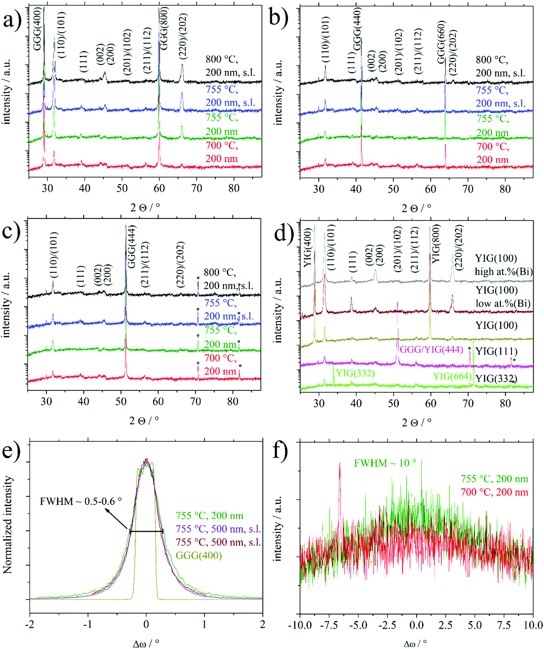 | ||
| Fig. 1 XRD 2Θ/ω scans of 200 nm BaTiO3 thin films deposited on GGG(100) (a), GGG(110) (b) and GGG(111) (c) and various YIG substrates (d) grown at different deposition temperatures, with or without a seeding layer (s.l.) and with different thicknesses on YIG substrates. Deposition conditions for YIG are: 700 °C, 200 nm for YIG(332), YIG(111) and YIG(100), as well as 755 °C, 500 nm, s.l. for YIG(100) with low and high at% (Bi) (see discussion below for details on Bi). The reflexes marked with * in (c and d) are further substrate reflexes. Uncommented miller indices are reflexes of BTO. The 2Θ/ω scan of a BTO film on YIG(111) (d) (pink colour) refers to the sample grown on YIG(111)/GGG(111), effectively a thin film of BTO grown on a thin film of YIG (∼160 nm thickness). Rocking curves of the BTO(110) reflex of thin films grown on GGG(100) (in green and violet) or YIG(100) (in brown) (e) or those grown on GGG(111) (f). | ||
| Substrate and procedure | TC(110) | TC(200) | TC(111) |
|---|---|---|---|
| GGG(110), 700 °C | 0.8 | 0.9 | 0.9 |
| GGG(110), 755 °C | 1.5 | 1.1 | 1.9 |
| GGG(100), 700 °C | 1.8 | 0.8 | 1.1 |
| GGG(100), 755 °C | 4.3 | 0.0 | 0.6 |
| GGG(100), 755 °C, s.l. | 4.2 | 0.3 | 0.2 |
| GGG(100), 800 °C, s.l. | 4.1 | 0.8 | 0.1 |
| YIG(332), 700 °C | 0.9 | 1.1 | 1.2 |
| YIG(100), 700 °C | 2.4 | 1.0 | 0.8 |
| YIG(100), 755 °C, s.l., high at% (Bi) | 4.3 | 0.6 | 0.1 |
| YIG(100), 755 °C, s.l., low at% (Bi) | 3.8 | 0.2 | 1.0 |
X-Ray photoelectron spectroscopy of BaTiO3 thin films
In order to further proof the quality of the prepared BTO thin films, XPS has been used to examine the stoichiometry. XPS interpretation of oxides is not a trivial task since samples exposed to or processed in ambient conditions often form hydroxides or carbonates on the surface. In addition, most oxides are insulators requiring usage of a flood gun and/or a charge correction. The latter is normally done to the ubiquitous adventitious hydrocarbon (C–C and C–H) and its respective C 1s signal, which is found on all ex situ samples. This procedure has been questioned.21 However, the consistency of binding energy values for the same components in this series of comparable samples lends credibility to the validness of this kind of charge correction in our study.Fig. 2 shows the XPS detail spectra of Ba 3d5/2, Ti 2p3/2, Ba 4d and O 1s of a 200 nm BTO film processed at 700 °C. For simplicity, only the first part of the doublet of the Ba 3d and Ti 2p photoelectron peak has been chosen. Especially, the estimation of the background for the Ti 2p3/2 fit could be worsened by the lack of undisturbed background at the higher binding energy side of the signal. Care has been taken to always use comparable total FWHM (±0.1 eV) and Gaussian and Lorentzian FWHM (G/L) for the same photoelectron line comparing the samples, i.e. approx. 1.5 eV (1.1 eV/0.7 eV), 1.3 eV (1.0 eV/0.7 eV), 1.4 eV (1.1 eV/0.4 eV) and 1.7 eV (1.5 eV/0.5 eV) for O 1s, Ti 2p3/2, Ba 4d and Ba 3d5/2, respectively. It is possible to use a more refined fit for the Ba 3d and Ti 2p spectra of these samples. Especially, the possible inclusion of the satellite structures at higher binding energies is rarely discussed in the literature. Also, the Ti 2p1/2 signal experiences special broadening effects, that decouples the normal quantum-mechanically proposed relationship between the two branches of a doublet.25 For the sake of this work, it is stated, that the “simple” procedure provides comparable results concerning the quantification to those obtained by a more complex fit including satellite features and signal broadening, as we determined within our research group.
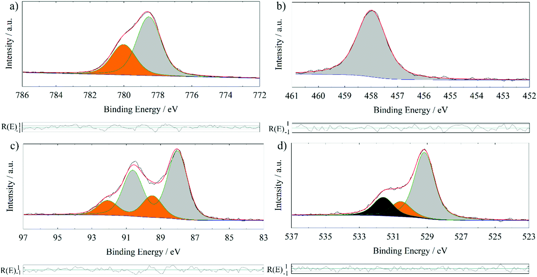 | ||
| Fig. 2 XPS detail spectra of a 200 nm BTO film processed at 700 °C on GGG(100); Ba 3d5/2 detail spectrum (a), Ti 2p3/2 detail spectrum (b), Ba 4d detail spectrum (c) and O 1s detail spectrum (d). | ||
In Table 2, XPS binding energies and quantifications of three different BTO films deposited at 700 °C on different garnet substrates are summarized. All fits are analogous to those shown in Fig. 2. The component at 778.5 ± 0.1 eV in Ba 3d5/2, the one at 529.1 ± 0.1 eV in O 1s and the peak at 458.0 ± 0.1 eV in the Ti 2p3/2 detail spectrum are attributed to bulk BTO. The comparison to the literature values in Table 3 support these assignments. This is substantiated by the relative quantifications of the “BTO bulk” components (Table 2) exhibiting ratios close to Ba1Ti1O3 considering the experimental relative error of about 10 per cent.
| Sample | BTO on YIG(100) | BTO on GGG(100) | BTO on YIG(332) |
|---|---|---|---|
| E B(O 1s) | 529.1(65.5)/530.9(19.2), 531.7(15.3) | 529.2(66.1)/530.6(15.3), 531.6(18.6) | 529.1(74.7)/530.4(10.8)/531.5(14.5) |
| E B(Ba 3d5/2) | 778.5(61.7)/780.1(38.4) | 778.5(65.8)/780.0(34.3) | 778.6(68.1)/780.1(31.9) |
| E B(Ba 4d5/2) | 88.0(72.6)/89.6(27.4) | 88.0(75.1)/89.5(24.9) | 88.0(77.1)/89.5(22.9) |
| E B(Ti 2p3/2) | 457.9 | 458.0 | 458.0 |
| [Ba778eV]/[Ti] | 1.2 | 1.1 | 1.2 |
| [O529eV]/[Ti] | 3.1 | 2.9 | 2.9 |
| [O529eV]/[Ba778eV] | 2.6 | 2.6 | 2.4 |
| [O531eV]/[Ba780eV] | 2.2 | 2.5 | 1.7 |
| At% (C) | 28.5 | 28.9 | 5.2 |
| Reference/sample | 26 | 28 | 29 | 34 *Ba(OH)2+BaCO3 | BTO polycr. | BTO(001) | BTO(111) |
|---|---|---|---|---|---|---|---|
| a Assigned by the authors to BaCO3. | |||||||
| Ba 3d5/2 (BTO bulk) | 778.3 | 778.4 | 778.8 | 778.6 | 778.5 | 778.4 | |
| Ba 4d5/2 (BTO bulk) | 88.1 | 88.1 | 88.0 | 87.9 | |||
| Ba 3d5/2 (contamination layer or amorphous overlayer on BTO) | 779.8a | 779.7 | 780.4 | 780.1 | 779.9 | 779.7 | |
| Ba 4d5/2 (contamination layer or amorphous overlayer on BTO) | 89.4a | 90.0* or 90.1+ | 89.5 | 89.4 | |||
| Ti 2p3/2 (BTO bulk) | 457.9 | 458.1 | 458.1 | — | 458.2 | 458.1 | 457.9 |
| O 1s (BTO bulk) | 529.1 | 529.3 | 529.5 | — | 529.4 | 529.3 | 529.2 |
| O 1s (O–H on BTO) | 531.1a | 531.0 | 531.1 | 530.8* | 530.8 | 531.1 | 530.8 |
| O 1s (O–C on BTO) | 532.5 | — | 532.3 | 531.7+ | 532.3 | 532.2 | 531.9 |
Whereas no further component is observed in the Ti 2p3/2 detail spectrum, the Ba 3d5/2 spectrum exhibits one further component at higher binding energy (780.0 ± 0.1 eV) and in O 1s two further components at higher binding energies (530.6 ± 0.3 and 531.6 ± 0.1 eV) are observed. Within the presented films, the high binding energy component in the Ba 3d5/2 detail spectrum is a surface component, as can be proven by inspecting the Ba 4d relative ratios (Table 2). The surface component at higher binding energy in Ba 4d (89.5 ± 0.1 eV) is consistently relatively lower than compared to the internal ratios in Ba 3d. This is due to the higher kinetic energy of Ba 4d photoelectrons which result in a higher inelastic mean free path and a lesser observation of surface components. Accepting the assignment of underlying bulk BTO, this surface component in Ba 3d5/2 should be purely consisting of Ba, C and O. There have been different approaches explaining the high binding energy component (that is always 1.3–1.6 eV higher than the bulk signal) in Ba 3d5/2 in BTO or BSTO in the literature:
•A surface contamination layer mainly consisting of Ba(OH)2, BaCO3 or a Ba–O-species is assumed.26,27
•A relaxed amorphous surface phase, often specified as under-coordinated Ba and discussed as an effect of the ferroelectric characteristics is proposed. To exclude the interpretation as a contamination layer, angle-dependent measurements after different treatments, including dipping in water and nitric acid, sintering the sample to get rid of carbonates and sputtering and annealing in UHV, have been performed.28–33
For the thin films in our study, a part of the high binding energy component in Ba 3d5/2 can be positively attributed to BaCO3, as we observe a signal at 288.8 ± 0.1 eV in the C 1s detail spectrum. However, heating a BTO film with significant high binding energy component to 475 °C in UHV led to a removal of the carbonate (as seen in the C 1s), but only a part of the further components in Ba 3d5/2 and O 1s (see ESI,† Fig. S1 and Table S2). Even though the O 1s components at approx. 530.6 and 531.6 eV of the BTO thin films discussed herein fit well to literature values of the hydroxides and carbonates (Tables 2 and 3). Thus we conclude, that in our samples both surface contaminations and a relaxed surface phase are responsible for the high binding energy component. Therefore, it may be hard to differentiate both scenarios in Ba 3d5/2 and O 1s spectra. However, in our case the surface phase should hardly contain any Ti, so an amorphous Ba–O-species with a composition of BaO or BaO2 is proposed.27 XPS quantification of both the high binding energy components in O 1s (530.6 and 531.6 eV, summarized as [O531eV]) against the Ba 3d5/2 signal at 780 eV yields ratios from 1.7–2.5. This may relate to a mixture of Ba(OH)2, BaCO3 and Ba–O-species in the surface phase. This quantification has to be considered tentatively, since the adventitious hydrocarbon on all ex situ samples normally also displays a minor amount of oxidized carbon species. The respective O 1s signal might also contribute, e.g. as C–OH, roughly at 531 eV.
The authors acknowledge, that some publications about BTO present other XPS absolute binding energy values for the respective photoelectron lines than the ones obtained in this study or included in Table 3.27,31,32 Looking more closely, all binding energy values are shifted by a respective value (so relative differences between photoelectron lines are well comparable to Tables 2 and 3), which indicates differences in the charge correction or instrument calibration. Finally, the XPS analysis confirms successfully deposited BTO thin films. Within this series of BTO deposition, there is no obvious correlation to synthesis parameters for the relative proportion of the second component at approx. 780.0 eV in the Ba 3d5/2 detail spectrum and approx. 89.5 eV in the Ba 4d detail spectrum.
XPS measurements of samples processed at 755 °C and 800 °C consistently exhibited comparably high amounts of Bi in the surface, up to 17 at% (metals basis, so [Bi]/([Bi] + [Ti] + [Ba])), whereas this value is ≤1.2 at% for Bi in samples deposited at 700 °C. This is due to cross-contamination from previous BiFeO3 growth in the same deposition chamber. Bi metal has a high vapour pressure, 1–2 Pa at 700 °C going up to approx. 15 Pa at 800 °C.35 Considering an ambient oxygen pressure of 25 Pa during deposition, unintended vapour deposition from contaminated parts inside the PLD chamber is very likely. The Bi amount in the surface increases with substrate temperature, in line with the increasing vapor pressure. An exemplary survey scan and Bi 4f detail spectrum of a 200 nm BTO thin film on GGG(100) deposited at 755 °C (with a seeding layer) are shown in Fig. 3. Representative XPS quantifications of samples processed at and above 755 °C are presented in ESI,† Table S3, alongside a discussion with aspects due to the Bi surface contamination. A sputter scan (shown in the ESI,† Fig. S2), i.e. sputtering with 1 keV Ar+-ions and intermitting XPS measurements, of a comparable sample revealed, that the Bi contamination is on the surface. Furthermore, bulk sensitive X-ray fluorescence spectroscopy provide an estimation of the overall content of Bi of approx. 1.6 at% (metals basis) for thin films deposited at 755 °C and usage of a seeding layer and 4.1 at% (metals basis) for those processed at 800 °C (data not shown here; these values should be considered with an estimated error of 30%, since the signal intensity is low and the right model for interpretation can only be assumed). It should be remarked here, that XPS is a surface sensitive method with an information depth of approximately 5 nm. Especially the first mean free path (1–2 nm) of the sample surface contributes most of the photoelectron intensity measured. Several Å of Bi or Bi-containing structures on the surface of the sample (see SEM measurements later on) can lead to an intense Bi 4f signal and the observed quantification results. The Bi surface concentration is also denoted on “metals basis”, which might be misleading, since significant substitution of Ba- and Ti-ions by Bi-ions is not to be assumed. XPS quantification is done under the assumption of a homogeneous sample, a prerequisite which is broken in this case and leads to apparently high at% of Bi through Bi-segregation to the surface. The Bi 4f detail scans from different samples are marked by two components, one at 157.1 ± 0.3 eV attributed to metallic Bi36 and one at 159.2 ± 0.3 eV assigned to Bi in an oxygen environment37 for the Bi 4f7/2 binding energy. It is hypothesized, that during deposition metallic Bi is evaporated on the surface of the sample through a contamination of the chamber, which is also used for BiFeO3 deposition. As a typical surfactant, Bi segregates to the surface during growth. After the end of the deposition and flooding of the chamber with 1 atm O2 at high temperatures, the metallic Bi is partly oxidized to Bi2O3. This assumption is supported by the fact, that metallic Bi is the dominating Bi species in 700 °C deposition (>50 at% within the overall low Bi content), whereas the Bi 4f detail spectrum of 800 °C deposited thin films almost exclusively exhibits Bi in an oxygen environment (see Table S3, ESI†). Higher temperatures while flooding with oxygen leads to a more thorough oxidation of the Bi metal located at the surface.
 | ||
| Fig. 3 XPS Bi 4f detail scan (a) and survey scan (b) of a 200 nm BTO thin film on GGG(100) processed at 755 °C (with seeding layer). Not all photoelectron lines of Bi are indicated in the survey scan for clarity. | ||
Preferential growth on GGG(100) and YIG(100) and the effect of an unintentional Bi surface contamination
As it is has been demonstrated in the first chapter, the preferential (110) BTO growth is only observed for the growth on GGG(100) and YIG(100). However, a further parameter has to be discussed as all the samples, on all substrate orientations, processed at 755 °C and above exhibited an unintentional Bi surface contamination as shown by XPS investigations. Since BTO thin films on GGG(110) and GGG(111) processed at 755 °C or higher are marked by low XRD intensities but still exhibit very similar Bi surface concentration as the films prepared on GGG(100) at the same temperature, a vital role of the substrate orientation has to be assumed. Thus, it shall be emphasized that the higher XRD intensity and higher texture coefficients of the (110) reflexes of the BTO films on GGG(100) and YIG(100) should strongly relate to the substrate orientation.However, comparing the growth within the samples deposited on GGG(100) and YIG(100), an influence of the Bi contamination on strain in the BTO(110) preferentially oriented films is assumed. Two thin films deposited at 755 °C are investigated closely for that question: one BTO/YIG(100) sample, called “low at% (Bi)” (Fig. 1(d)) contains roughly 6 at% (Bi) (metals basis, so [Bi]/([Bi] + [Ba] + [Ti])) or 2.2 at% (Bi) referring to BTO ([Bi]/([Ba] + [Ti] + [O])) as measured by XPS, which is mainly a surface concentration. The equivalent value for the sample “high at% (Bi)” (Fig. 1(d)) is approximately 15 at% (Bi) (metals basis) and 6–7 at% (Bi) (referring to BTO) surface concentration.
An induced strain in the BTO films can be deduced from a closer inspection of the 2Θ/ω XRD scans of the (110)/(101) reflexes shown in Fig. 4. In parallel to the higher intensity of the BTO(110) reflex for BTO thin films on garnet (100) substrates at higher temperatures, this reflex develops an asymmetric shape, which can be best observed in Fig. 4(b), indicating a further component. The latter observation can be interpreted as elongation of the interplanar spacing in z-direction (orthogonal to the surface) often caused by in-plane lattice strain of the thin film. At the bottom of Fig. 4(a), an unstrained low crystalline BTO thin film deposited at 700 °C exhibits a maximum in the 2Θ/ω scan at 31.48°. This position of the maximum with an error of ±0.03° is representative of all polycrystalline samples without or only low preferential orientation, i.e. all thin films deposited on the (110) and (111) substrate orientations and samples on (100) processed at 700 °C. As a further example, a BTO thin film deposited at 755 °C on GGG(111) in Fig. 4(a), that has considerable surface contamination of Bi, does not show a strained reflex. In correspondence with XPS results, the Bi is not significantly built into the BTO lattice. So the substrate-induced strain results in the asymmetry of the BTO(110) reflex and not unintentional Bi-doping.
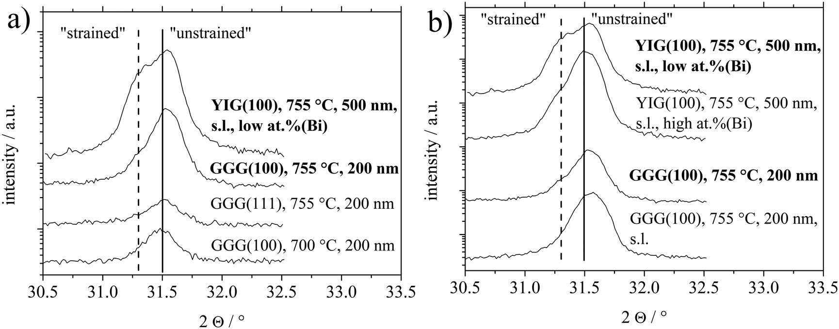 | ||
| Fig. 4 XRD 2Θ/ω scans in the range of the BTO(110)/(101) reflex of 200 nm and 500 nm BTO thin films on different YIG and GGG substrates (a) and the analogous comparison between a selected set on samples deposited solely on (100) orientations (b). Scans appearing in (a) and (b) are marked in bold scripture. | ||
Including the aspect of strain in the BTO(110) reflex, three effects of the Bi surface contamination are observed:
For the first aspect, it should be introduced, that in the intentional usage of a liquid surface layer for PLD, called tri-phase epitaxy, a quasi-equilibrium state between the growing thin film and a liquid surface layer is established.38–40 This enabled growth of highly single-crystalline thin films devoid of any crystallographic strain. Granted a similar role for the Bi surface contamination, which is liquid during deposition, high temperatures, usage of seeding layer (denoted as s.l.) and high Bi content should promote growth of strain-free thin films. This is best seen by direct comparison of BTO thin films on YIG(100) with low or high at% (Bi) and the couple of BTO thin films on GGG(100) with or without a seeding layer at 755 °C. In Fig. 4(b). Higher at% Bi and usage of the s.l. (for GGG(100)) reveals higher crystallinity by higher XRD intensity of BTO(110) reflexes.
Secondly, considering Fig. 4(b), samples without a seeding layer (denoted as s.l.) or in the case of the sample deposited on YIG(100) with low surface concentration of Bi (sample called “low at% (Bi)”), a more expressed shoulder at lower angles (∼31.3°) can be observed. And vice versa for using a seeding layer and relatively higher surface Bi contamination (sample called “high at% (Bi)”). This shift in 2Θ angle from 31.48° to roughly 31.3° equals a shift from interplanar spacing of the BTO(110) planes from 2.840 Å to 2.856 Å. Nominal values for d(BTO(110))/d(BTO(101)) are 2.828 Å/2.835 Å1 and 2.827 Å/2.840 Å42 depending on the ratio of c/a crystallographic axes in the tetragonal structure. As discussed later, this out-of-plane expansion might relate to a lowering of in-plane lattice misfit, in case of an edge-aligned epitaxy, since for an (110) oriented film, e.g. the [1−10] direction lies in-plane.
A third aspect can be suspected comparing the texture coefficients of samples on GGG(100) and YIG(100) processed at temperatures of 755 °C or higher in Table 1. Samples characterized by high at% (Bi) and/or usage of seeding layer show the BTO(100) orientation as the main alternative to BTO(110). Comparing surface energies, it is calculated that there are no significant differences between relaxed TiO2 or BaO terminated BTO(100) and O terminated BTO(110).41 For the simulations the BTO(110) had to be altered to not show an infinite dipole moment. Vice versa, less at% (Bi) or not using a seeding layer (in case of GGG(100)) seems to favor the BTO(111) grains as the main other orientation.
To summarize, the processing conditions high at% (Bi), seeding layer and higher temperatures promote a high intensity, strain-free BTO(110) reflex with the BTO(100) as the main alternative BTO orientation. The gradual absence of these processing conditions reveals lowered BTO(110) intensity, a more strained BTO(110) reflex and BTO(111) as the main alternative BTO orientation.
From this data, one could extrapolate, that approaching the situation with no Bi surface contamination should result in an even stronger strained BTO(110) reflex and BTO(111) grains as the other main orientation. At the least, the GGG(100) and YIG(100) orientation is a necessary prerequisite for BTO(110) growth, albeit the data cannot unequivocally prove, that it is a sufficient prerequisite.
It should be remarked here, that the BTO thin films with Bi surface contamination still show insulating properties as recorded in in-plane impedance spectroscopy measurements (not shown here).
The observed growth of BTO(110) on YIG(100)/GGG(100), in case of a strained BTO(110) reflex, can be described as “rectangle-on-cube”, as visualized in Fig. 5. The symmetry of the BTO(110) atomic planes is equal to a rectangle (see Fig. 5(c)). The YIG(100) or GGG(100) on which this BTO orientation is deposited has a quadratic unit cell as seen in the atomic plane (Fig. 5(c)). As an example the “edge aligned” in-plane epitaxial relationship is described in Fig. 5(d and e). Considering 2D point groups of the atomic planes of the substrate and the (110)-oriented BTO thin film, two rotational or mirror domains can be expected.43,44 For an exact assignment of this symmetry evaluation, the definitive atomic planes of YIG and BTO involved in the interface would have to be known. Phi-scans with asymmetrical reflexes of the BTO thin film and the substrate have been recorded and weak in-plane epitaxial relationships observed (see Fig. S3 and Table S4 in the ESI†). A discussion can also be found in the ESI.†
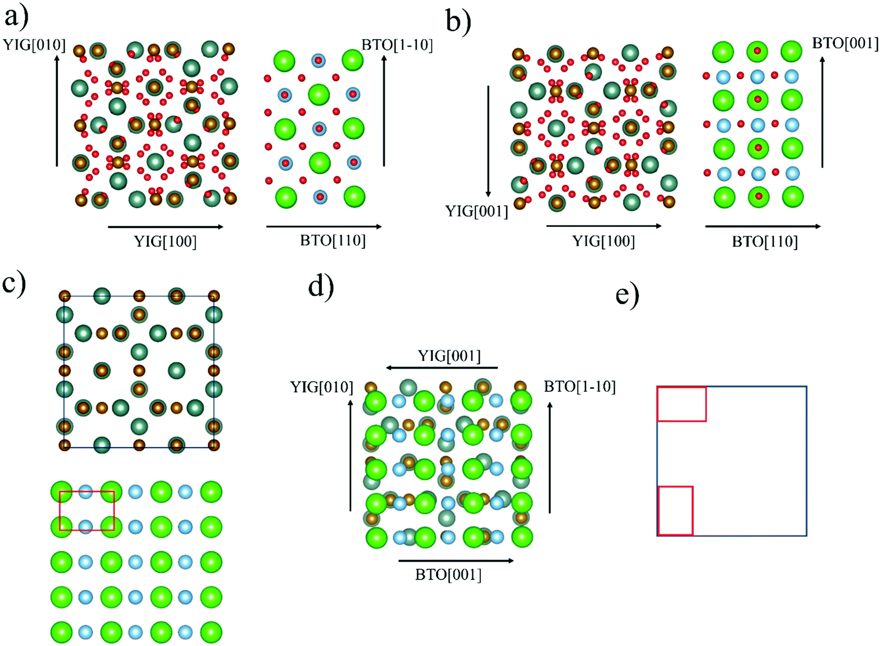 | ||
| Fig. 5 Visualization of proposed “rectangle-on-cube” growth of BTO(110) on YIG(100) or GGG(100) in “edge-aligned” configuration. Ba-Ions in green, Ti-ions in blue, O-ions in red, Fe-ions in brown and Y-ions in turquoise. For other configurations and discussion of epitaxial relationships, see Fig. S1 and Table S1 in ESI.† Side views (a and b) emphasizing the two different in-plane edge orientations BTO〈001〉‖YIG〈010〉 and BTO〈1−10〉‖YIG〈001〉. Top views on YIG(100) and BTO(110) (c), YIG(100) atomic plane schematically a square and BTO(110) atomic plane schematically a rectangle. “Edge aligned” rectangle-on-cube growth (d) displayed with metal ions (oxygen anions left out for all top view structures). In (e) schematic view with the two-domain growth as caused by rotational domains. All pictures (except (e)) are designed with the program Vesta.45 | ||
A case of “rectangle-on-cube” epitaxy is reported for the (110) oriented growth of SrRuO3 (SRO)(110) on Y-stabilised ZrO2 (YSZ)(100).46–48 Therein, a four-fold symmetry with an angle of 10° between SRO[001] and Y-stabilised ZrO2[010], that can be formally described as in-plane SRO[111]‖YSZ[110], is observed. The authors propose, that a decrease in lattice mismatch from 8.1%, in case of SRO(100)‖YSZ(100) and SRO[011]‖YSZ[010], to the rectangle-on-cube growth with −6.3% is the explanation for the unconventional case. It is also reported, that a relatively broad FWHM of 2.94° was found for the asymmetrical SRO(200) reflex used in the phi-scan. This is attributed to the still large in-plane lattice mismatch of the aforementioned value of −6.3%.48
Comparing this to BTO/YIG, the in-plane lattice mismatch for a cube-on-cube epitaxy, so BTO〈100〉‖YIG〈010〉 in-plane, of approx. 3% is relatively small. The in-plane lattice mismatch for the BTO(110) growth on YIG(100) and GGG(100) are generally higher (see Table S4 in ESI†), e.g. 2.6% (Fig. 5(a)) and 8.6% (Fig. 5(b)) for edge-aligned growth. The YIG(100) surface does not have a simple four-fold axis, but a four-fold screw axis and inversion axis (space group 230, Ia3d). Looking in [100] direction a common two-fold rotational symmetry can be identified. This might favour the growth of BTO(110), since both planes share the symmetry operation. Furthermore, only considering low-index orientation, BTO(110) and YIG(100) is a combination with highly charged atomic planes. So, theoretically BTO can grow on a purely oxygen terminated YIG(100) surface or BTO can grow with its oxygen plane on a Y/Fe terminated YIG(100) surface (this possibility is visualized in Fig. 5(a and b)).
To make an educated guess about successful cube-on-cube epitaxy, one could compare to the case of SrZrO3 on YIG or GGG(100). So, ferroelectric perovskites matching the cell parameter of SrZrO3 (∼4.102 Å) seem the most promising candidates. Unfortunately, most pseudocubic cell parameters for ferroelectric perovskites accumulate in the range 3.8–4.0 Å, e.g. Bi4Ti3O12, Sr2Bi2Ta2O9, NaNbO3 and BaTiO3.49 Only few examples are found with cell parameters above 4.00 Å, such as PMN–PT (∼4.02 Å) or KNbO3 (∼4.04 Å).49 The latter examples may be granted a higher tendency to grow with their (100) direction on a (100) garnet substrate.
Surface topography and morphology by AFM and SEM
Characterization of the topography of BTO thin films including surface roughness parameters are recorded by Atomic force microscopy (Fig. 6). Every column in Fig. 6 refers to one set of processing parameters and every row to one GGG substrate orientation. Inclusion of a seeding layer as well as raising processing temperature seems to favour the growth of bigger particles and a higher surface roughness, when following left to right in a row (for direct visual comparison of sizes, see insets in Fig. 6. Particles of BTO films processed at 755 °C without seeding layer (Fig. 6(b)) is characterized by spherical particles of about 120 nm and elongated ones which are roughly 250 nm long and few tens of nm broad. Furthermore, the particles especially at 800 °C deposition are needle-shaped and over 1 μm long in case of the BTO thin film on GGG(100) (Fig. 6(c)). The morphology is similar for all samples processed at 800 °C (Fig. 6(c, f and i)). | ||
| Fig. 6 AFM topography of BTO thin films on GGG(100)/(110)/(111) and YIG(100) substrates. In the comparison of growth on GGG substrates, the orientation is indicated at the left and the processing conditions on top. The insets in (b, c, e, f and (h–k)) are magnifications adjusted to (a, d and g), so displaying areas of 500 nm × 500 nm. Please note the different colouring for the height axis. RMS values are denoted in white and should be treated with a relative error of approximately 20%. Description of (j and k) is found directly next to the respective AFM pictures. | ||
Scanning electron microscopy (SEM) for samples grown on GGG(100) substrates (Fig. 7) exhibits morphologies and particle sizes similar to AFM results, while the signal of the back-scattered electrons allows for a detection of compositional differences. For the insulating samples measured in this work, electron microscopy at low voltages (2.0 kV) is employed to evade charging and achieve high surface sensitivity. Remarkably, samples grown at 755 °C and 800 °C show evenly-spaced dots with a size of approx. 2 to 5 nm in SE and BSE micrographs (Fig. 7(c–f)), and then bigger lumps on the surface for 800 °C deposited samples (see insets in Fig. 7(c and e)), that are interpreted as Bi/Bi2O3 particles. As these dots are seen in the topography-sensitive SE signal, it is confirmed, that the particles are situated on the top of the surface. XPS quantification revealed an increase of Bi surface concentration (metals basis) from 700 °C to 755 °C and then to 800 °C of around 1 at%, 15 at% and approx. 17 at%. Accordingly, the size and density of the bright spots, which are caused by higher backscattering of the heavy Bi atoms in BSE (Fig. 7(d and f)), increases with temperature. Bi droplet formation on the surface, e.g. in molecular beam epitaxy of Bi-containing III/V semiconductors, is common, though the formed drops are bigger.50,51 It is speculated, that the drop-like Bi-containing particles do not coalesce, since, at higher temperatures, they are oxidized to Bi2O3 as proven by XPS. It should be remarked, that in AFM microscopy, those dot features are not resolved, as the measured topography is a convolution of tip size (specified as ≤10 nm) and the objects. Furthermore, rough surfaces can damage or contaminate the tip and obscure the measured shape. While Fig. 7 focuses on the distribution of Bi on the surface, large area BSE scans show different crystallite orientations. In the preferentially oriented (110) BTO thin films grown on GGG(100) both at 755 °C and 800 °C, the needle-shaped crystallites could therefore be related to (110) oriented BTO crystallites, which dominate the scan (not shown here) in comparison to BSE scans on a BTO thin film on GGG(110).
 | ||
| Fig. 7 SEM micrographs acquired as the secondary electron (SE) and back-scattered electron (BSE) signal of the same spot within each sample. BTO thin films deposited on GGG(100) at 700 °C (a and b), 755 °C with seeding layer (c and d) and 800 °C with seeding layer (e and f). Enhanced insets (zoom factor: 4) in (c and e) emphasize Bi/Bi2O3 particles, which appear brighter. The scale as depicted in (e) is valid for all micrographs shown. | ||
Conclusions
We have demonstrated that preferentially (110)-oriented BTO thin films (200–500 nm) can be grown on GGG(100) and YIG(100) by pulsed laser deposition. These thin films display significantly higher X-ray diffraction reflex intensities compared to growth on GGG(110) and GGG(111), as well as a weak in-plane “rectangle-on-cube” ordering. Possible explanations in terms of in-plane lattice mismatch and symmetry considerations are discussed. By comparing different films grown on GGG(100) and YIG(100), a surfactant-induced effect by a Bi surface contamination on BTO(110) strain and epitaxial coherence is proposed. After deposition, the Bi seems to remain on the surface as oxidized Bi/Bi2O3 droplets, which are a few nm in size. XPS measurements are interpreted separating the Ba 3d5/2 and Ba 4d detail spectra into a BTO bulk and a surface species.As microwave dual-tunability is conceptually not dependent on coupling between the ferroelectric and ferro(i)magnetic phase, a better crystallinity of the BTO thin film, as achieved on a GGG(100) or YIG(100) substrate, could be sufficient for improving device qualities. In contrast to that, strain-mediated magnetoelectric coupling, e.g. for shifting the FMR line position, elastic coupling and therefore strained BTO films are more promising. Synthesis of edge-aligned “rectangle-on-cube” epitaxy is favourable there.
Conflicts of interest
There are no conflicts to declare.Acknowledgements
The authors are indebted to Holger Hochmuth for technical support with the BTO deposition chamber. Furthermore, the authors would like to thank Paula Huth for measurement of the BTO standard samples. This research work was partly financed by Deutsche Forschungsgemeinschaft (DFG) in the framework of SFB 762 “Functionality of oxide interfaces”.References
- R. H. Buttner and E. N. Maslen, Acta Crystallogr., Sect. B: Struct. Sci., 1992, 48, 764 CrossRef.
- M. G. Harwood, P. Popper and D. F. Rusman, Nature, 1947, 160, 58–59 CrossRef CAS PubMed.
- F. Euler and J. A. Bruce, Acta Crystallogr., 1965, 19, 971 CrossRef CAS.
- D. Rodic, M. Mitric, R. Tellgren, H. Rundlof and A. Kremenovic, J. Magn. Magn. Mater., 1999, 191, 137 CrossRef CAS.
- W. Noun, E. Popova, F. Bardelli, Y. Dumont, R. Bertacco, A. Tagliaferri, M. Tessier, M. Guyot, B. Berini and N. Keller, Phys. Rev. B: Condens. Matter Mater. Phys., 2010, 81, 054411 CrossRef.
- J. Sasvári and P.-E. Werner, Acta Chem. Scand., Ser. A, 1983, 37, 203 CrossRef.
- C. Hauser, T. Richter, N. Homonnay, C. Eisenschmidt, M. Quaid, H. Deniz, D. Hesse, M. Sawicki, S. G. Ebbinghaus and G. Schmidt, Sci. Rep., 2016, 6, 20827 CrossRef CAS PubMed.
- J. H. Leach, H. Liu, V. Avrutin, E. Row, Ü. Özgür, H. Morkoc, Y.-Y. Song and M. Wu, J. Appl. Phys., 2010, 108, 064106 CrossRef.
- Q. X. Jia, J. R. Groves, P. Arendt, Y. Fan, A. T. Findikoglu and S. R. Foltyn, Appl. Phys. Lett., 1999, 74, 1564 CrossRef CAS.
- J. Das, Y.-Y. Song, N. Mo, P. Krivosik and C. E. Patton, Adv. Mater., 2009, 21, 2045 CrossRef CAS.
- J. Lian, F. Ponchel, N. Tiercelin, Y. Chen, D. Rémiens, T. Lasri, G. Wang, P. Pernod, W. Zhang and X. Dong, Appl. Phys. Lett., 2018, 112, 162904 CrossRef.
- G. Dong, Z. Zhou, X. Xue, Y. Zhang, B. Peng, M. Guan, S. Zhao, Z. Hu, W. Ren, Z.-G. Ye and M. Liu, ACS Appl. Mater. Interfaces, 2017, 9, 30733 CrossRef CAS PubMed.
- A. A. Semenov, S. F. Karamenko, V. E. Demidov and B. A. Kalinikos, Appl. Phys. Lett., 2002, 88, 033503 CrossRef.
- A. B. Ustinov, G. Srinivasan and B. A. Kalinikos, Appl. Phys. Lett., 2007, 90, 031913 CrossRef.
- S. Shastry, G. Srinivasan, M. I. Bichurin, V. M. Petrov and A. S. Tatarenko, Phys. Rev. B: Condens. Matter Mater. Phys., 2004, 70, 064416 CrossRef.
- Y. K. Fetisov and G. Srinivasan, Appl. Phys. Lett., 2006, 88, 143503 CrossRef.
- G. Schileo, A. Feteira, I. M. Reaney, P. Postolache, L. Mitoseriu and K. Reichmann, Int. J. Appl. Ceram. Technol., 2014, 11, 457 CrossRef CAS.
- A. Pique, K. S. Harshavardhan and T. Venkatesan, US Pat., 5635453, 1997.
- L. S. Cavalcante, A. Z. Simões, J. C. Sczancoski, V. M. Longo, R. Erlo, M. T. Escote, E. Longo and J. A. Varela, Solid State Sci., 2007, 9, 1020 CrossRef CAS.
- M. C. Onbasil, A. Kehlberger, D. H. Kim, G. Jakob, M. Kläui, A. V. Chumak, B. Hillebrands and C. A. Ross, APL Mater., 2014, 2, 106102 CrossRef.
- G. Greczynski and L. Hultman, Prog. Mater. Sci., 2020, 107, 100591 CrossRef CAS.
- D. A. Shirley, Phys. Rev. B: Solid State, 1972, 5, 4709 CrossRef.
- R. Hesse, T. Chassé and R. Szargan, Anal. Bioanal. Chem., 2003, 375, 856 CrossRef CAS PubMed.
- G. B. Harris, London, Edinburgh Dublin Philos. Mag. J. Sci., 1952, 43, 113 CrossRef.
- P. S. Bagus, C. J. Nelin, C. R. Brundle and S. A. Chambers, J. Phys. Chem. C, 2019, 123, 7705 CrossRef CAS.
- C. Miot, E. Husson, C. Proust, R. Erre and J. P. Coutures, J. Mater. Res., 1997, 12, 2388 CrossRef CAS.
- Y. Fujisaki, Y. Shimamoto and Y. Matsui, Jpn. J. Appl. Phys., 1999, 38, L52 CrossRef CAS.
- J. L. Wang, A. Pancotti, P. Jégou, G. Niu, B. Gautier, Y. Y. Mi, L. Tortech, S. Yin, B. Vilquin and N. Barrett, Phys. Rev. B: Condens. Matter Mater. Phys., 2011, 84, 205426 CrossRef.
- D. Ehre, H. Cohen, V. Lyahovitskaya and I. Lubomirsky, Phys. Rev. B: Condens. Matter Mater. Phys., 2008, 77, 184106 CrossRef.
- J. D. Baniecki, M. Ishii, T. Shioga and K. Kurihara, Appl. Phys. Lett., 2006, 89, 162908 CrossRef.
- S. M. Mukhopadhyay and T. C. S. Chen, J. Mater. Res., 1995, 10, 1502 CrossRef CAS.
- A. Berlich, H. Strauss, C. Langheinrich, A. Chassé and H. Morgner, Surf. Sci., 2011, 605, 158 CrossRef CAS.
- M. Wegmann, L. Watson and A. Hendry, J. Am. Ceram. Soc., 2004, 87, 371 CrossRef CAS.
- O. Karslioğlu, L. Trotochaud, I. Zegkinoglou and H. Bluhm, J. Electron Spectrosc. Relat. Phenom., 2018, 225, 55 CrossRef.
- Smithsonian Physical Tables 9th ed., online version (1954, Knovel 2003), Table 363, Evaporation of metals.
- C. J. Powell, J. Electron Spectrosc. Relat. Phenom., 2012, 185, 1 CrossRef CAS.
- K. Uchida and A. Ayame, Surf. Sci., 1996, 170, 357–358 Search PubMed.
- K. S. Yun, B. D. Choi, Y. Matsumoto, J. H. Song, N. Kanda and T. Itoh, Appl. Phys. Lett., 2002, 80, 61–63 CrossRef CAS.
- R. Takahashi, Y. Matsumoto, T. Kohno, M. Kawasaki and H. Koinuma, J. Cryst. Growth, 2004, 262, 308–312 CrossRef CAS.
- R. Takahashi, Y. Yonezawa, M. Ohtani, M. Kawasaki, K. Nakajima, T. Chikyow, H. Koinuma and Y. Matsumoto, Adv. Funct. Mater., 2006, 16, 485–491 CrossRef CAS.
- R. I. Eglitis, G. Borstel, E. Heifets, S. Piskunov and E. Kotomin, J. Electroceram., 2006, 16, 289 CrossRef CAS.
- C. M. Culbertson, A. T. Flak, M. Yatskin, P. H.-Y. Cheong, D. P. Cann and M. R. Dolgos, Sci. Rep., 2020, 10, 3729 CrossRef CAS PubMed.
- M. Grundmann, T. Böntgen and M. Lorenz, Phys. Rev. Lett., 2010, 105, 146102 CrossRef PubMed.
- M. Grundmann, Phys. Status Solidi B, 2011, 248, 805 CrossRef CAS.
- K. Momma and F. Izumi, J. Appl. Crystallogr., 2011, 44, 1272 CrossRef CAS.
- H. N. Lee, S. Senz, A. Visinoiu, A. Pignolet, D. Hesse and U. Gösele, Appl. Phys. A: Mater. Sci. Process., 2000, 71, 101 CrossRef CAS.
- S. Y. Hou, J. Kwo, R. K. Watts and J.-Y. Cheng, Appl. Phys. Lett., 1995, 67, 1387 CrossRef CAS.
- A. Chopra, M. Alexe and D. Hesse, J. Appl. Phys., 2015, 117, 044102 CrossRef.
- A. R. Damodaran, J. C. Agar, S. Pandya, Z. Chen, L. Dedon, R. Xu, B. Apgar, S. Saremi and L. W. Martin, J. Phys.: Condens. Matter, 2016, 28, 263001 CrossRef PubMed.
- G. Vardar, S. W. Paleg, M. V. Warren, M. Kang, S. Jeon and R. S. Goldman, Appl. Phys. Lett., 2013, 102, 042106 CrossRef.
- M. Oliva, G. Gao, E. Luna, L. Geelhaar and R. B. Lewis, Nanotechnology, 2019, 30, 425601 CrossRef CAS PubMed.
Footnote |
| † Electronic supplementary information (ESI) available. See DOI: https://doi.org/10.1039/d2ma00041e |
| This journal is © The Royal Society of Chemistry 2022 |