
 Open Access Article
 This Open Access Article is licensed under a Creative Commons Attribution-Non Commercial 3.0 Unported Licence
Giant valley splitting in a MoTe2/MnSe2 van der Waals heterostructure with room-temperature ferromagnetism†
Qianze
Li
 ab,
Cai-xin
Zhang
b,
Dan
Wang
c,
Ke-Qiu
Chen
b and
Li-Ming
Tang
*b
ab,
Cai-xin
Zhang
b,
Dan
Wang
c,
Ke-Qiu
Chen
b and
Li-Ming
Tang
*b
aSchool of Physics and Chemistry, Hunan First Normal University, Changsha 410205, China
bDepartment of Applied Physics, School of Physics and Electronics, Hunan University, Changsha 410082, China. E-mail: lmtang@hnu.edu.cn
cInstitute of Mathematics and Physics, Central South University of Forestry and Technology, Changsha 410018, China
First published on 11th February 2022
Abstract
An intrinsic large valley splitting has been realized in van der Waals (vdW) heterostructures formed by monolayer MoTe2 and layered room-temperature ferromagnetic MnSe2via first-principles calculations. The value of valley splitting of MoTe2 can reach 106 meV among a variety of stacking MoTe2/MnSe2 heterobilayers, which is equivalent to the effective Zeeman splitting in an external magnetic field of 530 T. And the magnitude of valley splitting can be further enhanced by applying external vertical-stress and biaxial compressive strain. To obtain a higher operating temperature, a biaxial tensile strain of 2.3% has been applied on the monolayer MnSe2 magnetic substrate, and the corresponding Curie temperature increased from an intrinsic value of 266 K to 353 K, but the valley splitting can still remain as large as 72 meV. This means that we can strike a balance between large valley splitting and high Curie temperature, which is vital for the application of magnetic valley electronic devices.
Introduction
In the H-type monolayer transition metal dichalcogenides MX2 (M = Mo, W; X = S, Se, Te), the electronic and hole carriers at the two energy degenerate but inequivalent K and K′ valleys are associated with some special valley-contrasting physical properties, such as the Berry curvature and spin-valley Hall effects, which is believed to be used for new memory and logic applications.1–3 However, protected by the time-reversal symmetry, the carriers at the two valleys are balanced so that the intrinsic pure spin-valley Hall current cannot be obtained between the two valleys. Therefore, breaking the balance of the carriers, i.e., lifting the valley degeneracy is an indispensable step towards the applications of valleytronic devices.4,5The feature of spin–valley locking provides broad ways to achieve valley polarization, such as optical pumping,6–9 external magnetic field,10,11 magnetic doping,12–15 and forming vertical heterostructures with magnetic materials.16–26 From the perspective of achieving large and stable valley splitting, none of the first three cases is the best choice because they are limited by the manipulating robustness, stability of the doped systems, and a tiny valley splitting efficiency (∼0.2 meV T−1),10,11 respectively, which are far from the requirements of practical applications. Conversely, realizing this goal via magnetic proximity effects between magnetic materials and TMDs, namely, forming TMD/magnetic material heterostructures, appears more promising.20,26 Before two-dimensional (2D) magnets were successfully fabricated through experiments,27,28 several notable examples of placing monolayer TMDs upon bulk (3D) magnetic substrates to form 2D/3D heterostructures, such as TMDs/EuO(EuS)16,17 and n-WS2/p-(Ga,Mn)As,29 have been utilized to manipulate valley splitting, in which a large substantial valley splitting of 44 meV was predicted theoretically in MoTe2/EuO [16], and a very recent experiment reported that the splitting efficiency in TMDs/EuS reached a value of 16 meV T−1.19 Additionally, to optimize the magnetic substrates, many 2D-magnet/TMD vdW heterostructures have also been tried both experimentally and theoretically, such as CrI3/WSe2,20,21 NiCl2/WTe2,22 and h-VN/WS2,23 where not only a considerable splitting size was obtained, but also the superiority of 2D/2D systems was verified. More importantly, the reports further demonstrate that large interlayer charge transfer is a key factor in the formation of large valley splitting, which can enhance the magnetic proximity coupling between TMDs and magnetic substrates, and ultimately enlarge the valley splitting. We made it clear in our previous work that this situation is more likely to occur in the heterostructure of type-III band alignment with large charge transfer.22 Additionally, the splitting size is positively correlated with interfacial atom superposition, especially the superposition between the metal atoms.21,22 This means that a magnetic material which can form a type-III band alignment and has the same hexagonal crystal structure and similar lattice constants to TMDs will be the ideal substrate.
Though considerable progress has been made, there is a problem to be faced: the Curie temperatures of the above substrates, and even for the most insulating ferromagnetic materials, are typically very low,27,28,30 well below room temperature, and their use as substrate materials will eventually hinder the practical application of valleytronic devices. The recent experimental results also confirmed that the valley splitting efficiency in magnet/TMD samples decreases significantly with the increase of experimental temperatures.19 Therefore, it is of great significance to select magnetic substrates which can not only induce large valley splitting, but also have a high Curie temperature from so many 2D magnetic materials.31–34 The monolayer 1T-MnSe2 is reported to exhibit intrinsic room-temperature ferromagnetism,35–37 the same hexagonal crystal structure, and similar lattice constants to TMDs, suggesting that it is highly likely to cause large valley splittings.
In this work, a MoTe2/MnSe2 heterobilayer with six different stacking structures has been studied to obtain large valley splittings. Our results show that the largest intrinsic total valley splitting in the MoTe2 layer can reach 106 meV, equivalent to the effective splitting under an external magnetic field of 530 T, and the value can be further increased by applying external vertical-stress and biaxial strain. Additionally, the combination of density functional theory (DFT) and Monte Carlo (MC) simulations shows that the Curie temperature of the MnSe2 substrate can be easily increased above room temperature under appropriate tensile strain, and the valley splitting in MoTe2 can still remain as large values.
Results and discussion
The 1T-phase monolayer MnSe2 has the same hexagonal crystal structure as the 2H-type monolayer TMDs, where the Se–Mn–Se atoms in the unit cell are connected in a sandwich structure, and the two Se atoms are not equivalent.35-37 The optimized in-plane lattice constants of the pristine monolayer MnSe2 and MoTe2 are 3.65 Å and 3.55 Å, respectively, with a lattice mismatch of 2.8%. According to the structural characteristics, three pairs of typical stackings, containing a total of six different stable stacking configurations, are considered. The six stackings are denoted as (S-1/S-1′), (S-2/S-2′), and (S-3/S-3′), respectively, which are presented in Fig. 1. After full relaxation, the optimized in-plane lattice constants (a0s) of all six stackings are the same, with a value of 3.56 Å, but the interlayer distances (d0s) are different. We noted that (S-1/S-1′) has a feature of Mo and Se atoms completely overlapping (Mo⊥Se), and the difference is that the Mo of S-1 overlaps with the interfacial Se1 atom (Mn⊥Se1), while the Mo of S-1′ overlaps with the non-interfacial Se2 atom (Mn⊥Se2). By analogy, (S-2/S-2′) has Mn and Mo atoms completely overlapping (Mo⊥Mn), and for (S-3/S-3′), there is neither Mn and Mo overlap nor Mn and Te overlap, see Fig. 1. In fact, S-1′ and S-2′ (S-3′) can be seen as 60°(180°) counterclockwise rotations of S-1 and S-2 (S-3) while keeping the MnSe2 layer stationary. Therefore, for the monolayer MoTe2, the Brillouin zone K high-symmetry point in S–N corresponds to the K′ point in the S–N′ stacking. This structural property allows the magnetic substrate to be moved or rotated to adjust the size and direction of valley splittings. To determine the structural stability and the most stable stacking configuration, the binding energies Eb of the six configurations are calculated using the formula, Eb= EMoTe2/MnSe2 − EMoTe2 − EMoSe2, where EMoTe2/MnSe2, EMoTe2, and EMoTe2 are the total energies of the MoTe2/MnSe2 heterobilayer, pristine MoTe2 and MnSe2 monolayer, respectively. The values of Eb for all of these heterobilayers are rather close and have negative values of about −0.27 eV, −0.29 eV, −0.27 eV, −0.17 eV, −0.17 eV, and −0.27 eV, respectively, which indicates that these heterostructure configurations are energetically favorable.38 It is noteworthy that VS2/TMD heterostructures with the same structure have been successfully prepared by experiments,39 so MnSe2/MoTe2 could also be prepared.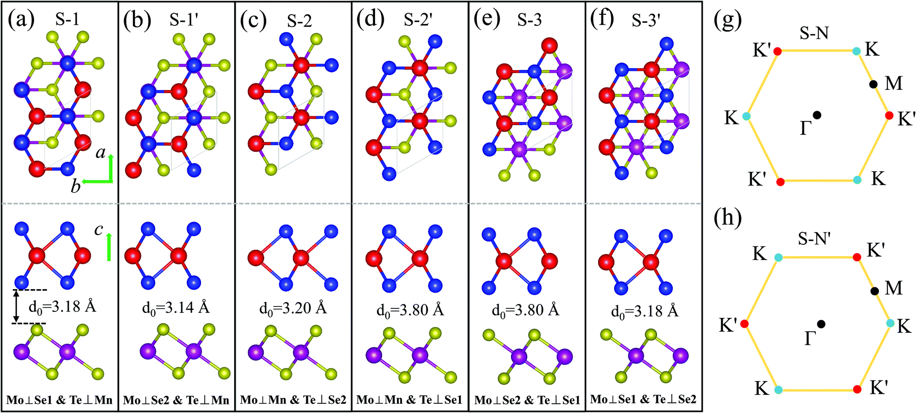 | ||
| Fig. 1 Configurations and Brillouin zone of the MoTe2/MnSe2 heterostructure in six stackings. (a–f) Top and side views of the heterobilayer in six stackings. (g) and (h) First Brillouin zone of S-N and S-N′ stackings, respectively. The K(K′) in the S–N corresponds to the K′(K) point in the S–N′ for MoTe2. The rhombus indicates a unit cell. The red, blue, purple, and yellow balls represent the Mo, Te, Mn, and Se atoms, respectively. Se1 and Se2 correspond to the interfacial and non-interfacial atoms, respectively. | ||
Fig. 2 presents the band structures of the six different stacked MoTe2/MnSe2 heterobilayers, and the corresponding enlarged details of valley splitting of the MoTe2 monolayer. It is found that the band-edge of monolayer MnSe2 near the Fermi-level is almost composed of Mn-3d orbitals and Se-p orbitals, and the valence band maximum (VBM) at K is spin-down, while the conduction band minimum (CBM) is spin-up, exhibiting ferromagnetic conducting properties. The magnetic moments of the Mn and Se atoms are 3.99 and −0.37 μB, respectively (see Fig. S1 in the ESI†).40 The band-edges of MoTe2 and MnSe2 layers are strongly hybridized at the Γ point, but much weaker at the K point. For the MoTe2 monolayer, the spin states of the valence and conduction bands of the S–N and S–N′ stacking at the K/K′ valleys are opposite when the same Brillouin-zone is used to calculate the band structures, see Fig. 2(a). The valley splitting is the energy difference between the two valley extrema of MoTe2,16i.e., 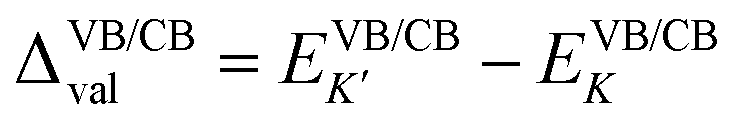 and the total valley splitting is derived as ΔKK′ = ΔVB − ΔCB. As shown in Fig. 2(b), valley splittings are indeed achieved in all stackings, and the size in S-1′ is the largest, with values of −90 and 16 meV for ΔVB and ΔCB, respectively. As shown in Fig. 2(b), the valley splittings are indeed achieved in all stackings, and the size in S-1′ is the largest, with values of −90 and 16 meV for ΔVB and ΔCB, respectively. So, the total K−K′ valley splitting reaches a giant value of 106 meV. Considering the measured Zeeman valley-splitting rate of ∼0.2 meV T−1 in monolayer TMDs, its equivalents to the splitting by a 530 T external magnetic field. This value is tens of times the splitting strength achieved in CrI3/WSe2,20,21 and even exceeds the substantial values that can be obtained in some typical heterostructures [see Table S1 in the ESI† for details].40–43 Owing to the large energy difference (i.e., valley splitting) between K and K′, optical excitation is used to obtain spin-valley excitons on the two valleys in a considerable spectral frequency range (E = ħω) by optical frequency tuning, thus making it easy to achieve stable pure spin-valley currents from the two valleys. The valence-band valley splitting is also very close to the Fermi level, so it will be easier to excite the valley carriers experimentally.
 | ||
| Fig. 2 (a) Band structure of the MoTe2/MnSe2 heterobilayer in six stackings. The Fermi energy level is set to zero. (b) The corresponding enlarged details of valley splitting for the MoTe2 monolayer. The red and blue lines denote the spin-up and spin-down bands, respectively, for the monolayer MoTe2. ΔVB and ΔCB are the valence- and conduction-band valley splittings, respectively. | ||
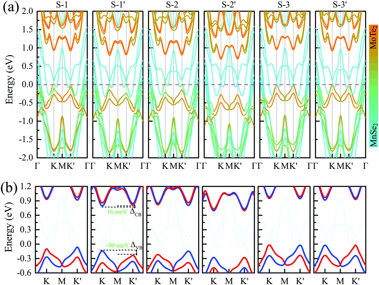
Additionally, an out-of-plane magnetic moment of 0.008–0.034 μB is induced at the Mo atoms in six different stacked heterobilayers, which indicates that the time-reversal symmetry of MoTe2 is broken by MnSe2. To further confirm that, we have also calculated the Berry curvature based on Wannier functions in Fig. 3. Note that due to the strong hybridization between MoTe2 and MnSe2 at Γ, we mainly focus on the Berry curvature near K and K′ valleys, because the valley-excitons near the two valleys have stable valley-dependent pseudo magnetic moments and optical transition selection rules. As shown in Fig. 3(a), the MLWFs calculated band structure coincided well with the DFT calculations [Fig. 2(a)], indicating that the constructed Wannier base functions are credible. And the opposite signs of the Berry curvature near the two valleys indicate that the spin–valley properties are still well preserved, and the unequal absolute value means that the time reversal symmetry of the monolayer MoTe2 has been broken by the magnetic substrate, see Fig. 3(b). Therefore, it is convinced that MnSe2 can produce magnetic proximity effects with monolayer MoTe2 to induce valley splitting.
 | ||
| Fig. 3 (a and b) MLWF calculated band structure and the corresponding Berry curvature of the monolayer MoTe2 in the heterobilayer, respectively. | ||
To study the effect of stacking on valley splitting, we list the valley splitting size and related structural parameters for the six different stackings for comparison in Table 1. It is noted that for MoTe2, the valence band edges at the K and K′ valleys are mostly composed of 4d states of Mo atoms and a rather small amount of p (and s) states of Te atoms. For the MnSe2 substrate, the conduction band edge at K/K′ is mainly composed of Mn-dxz and a little Se-pz. Therefore, the coupling between the Mo–Mn and Mn–Se atoms is the decisive factor affecting valley splitting, while the coupling between Te–Mn and Te–Se atoms has little influence on the valley splitting size. Considering that the splitting size is mainly related to the coupling effect of the Mo atom between the Mn and interfacial Se1 atoms, only the equilibrium interlayer spacing d0, dMn–Mo, and dMn–Te1 are counted. As shown in the table, a large valley splitting can be achieved in S-1, S-1′ and S-2, and it is one order of magnitude larger than those of the last three stacked structures. This is mainly because the first three stacking structures have a smaller d0 and dMn–Mo, and a large atomic overlap rate between the two layers, especially the overlap rate with magnetic Mn atoms. The results are very similar to the situation in the NiCl2/WTe2 heterobilayer, which is with a type-III band alignment.22 The difference is that MnSe2 is a magnetic metal substrate, and it will further enhance the Coulomb attraction between MnSe2 and MoTe2, resulting in a decrease in the interlayer spacing, and ultimately leading to a larger valley splitting. By comparing the cases of S-1 and S-1′, they have similar stacking, and almost the same d0 and dMn–Mo, whereas the overlap ratio between Mn and Mo in S-1′ is much larger than that of S-1, resulting in the splitting of S-1′ being much larger than that of S-1. This is because the dominant part of the magnetic proximity coupling between MnSe2 and MoTe2 is the coupling between the d orbitals of the two metal atoms, and the easy magnetization axis of the d orbital of MoTe2 is in the vertical direction. Therefore, the closer the distance between the two atoms, the greater the overlap rate, the stronger the coupling effect, and ultimately the larger the valley splitting. This can also be further confirmed from the situation of S-1 and S-3′, which have the same d0 and dMn–Mo, but S-3′ does not have Mn, Mo and Te atoms directly covered, leading to the total splitting value being much smaller than that of S-1. And interestingly, S-1′ stacking has the largest valley splitting, indicating that the coupling strength between MoTe2 and MnSe2 is the largest, which will decrease the system energy. This also explains why S-1′ stacking is the most stable configuration.
| Stacks | d 0 (Å) | d Mn–Mo (Å) | d Mn–Te1 (Å) | d Te–Se1 (Å) | Δ VB (meV) | Δ VB (meV) | Δ KK′ (meV) |
|---|---|---|---|---|---|---|---|
| S-1 | 3.18 | 6.79 | 4.99 | 3.78 | 37.8 | −14.1 | 51.9 |
| S-1′ | 3.14 | 6.73 | 5.35 | 3.75 | −90 | 16 | 106 |
| S-2 | 3.20 | 6.47 | 5.41 | 3.80 | 70.5 | −13.3 | −83.3 |
| S-2′ | 3.80 | 7.10 | 5.98 | 3.80 | −1.4 | 0.8 | 2.2 |
| S-3 | 3.80 | 7.38 | 5.97 | 3.80 | −5 | −5.2 | −0.2 |
| S-3′ | 3.18 | 6.77 | 4.99 | 3.79 | 3.6 | 12.3 | 8.7 |
To further explain why valley splitting varies so much between different stackings, we have also calculated the charge density distribution of the six stackings in Fig. S2 (see the ESI†).40 The results show that the splitting size in S-2′ and S-3 is much smaller than that of the other four stackings, which is mainly because its interlayer charge transfer is significantly smaller than the former cases. Although S-3′ also has a large charge transfer, the charge density distribution around Mo is much smaller than that of the first three stackings, so the splitting intensity is relatively small. This also directly reflects that the charge transfer and the magnetic coupling between MnSe2 (magnetic material) and MoTe2 (monolayer TMDs), especially the coupling between (magnetic atoms) Mn and Mo/W atoms, are the key factors affecting valley splittings. The results are in good agreement with the results of previous works,21,22 which will provide a reliable way to achieve large valley splitting in a 2D magnet/TMD vdW heterostructure.
Now that valley splitting is closely related to layer spacing, it is natural to regulate the splitting size by applying vertical stress, which can be experimentally adjusted by inserting dielectric layers or by applying vertical pressure directly.44 Considering that S-1′ stacking is the most stable configuration, it will be used as an example in the following studies. As presented in Fig. 4(a), the ΔVB and ΔCB values of MoTe2 vary linearly with the interlayer spacing d0. When d0 decreases, the magnitude of total valley splitting ΔKK′ (ΔKK′ = ΔVB − ΔCB) increases; conversely, ΔKK′ decreases. When d0 reduces to a critical value of 2.54 Å (if d0 is further reduced, the energy-valley structure of MoTe2 will be destroyed), ΔKK′ reaches the maximum value of 138.6 meV, equivalent to the splitting size caused by an effective external magnetic field of 693 T.
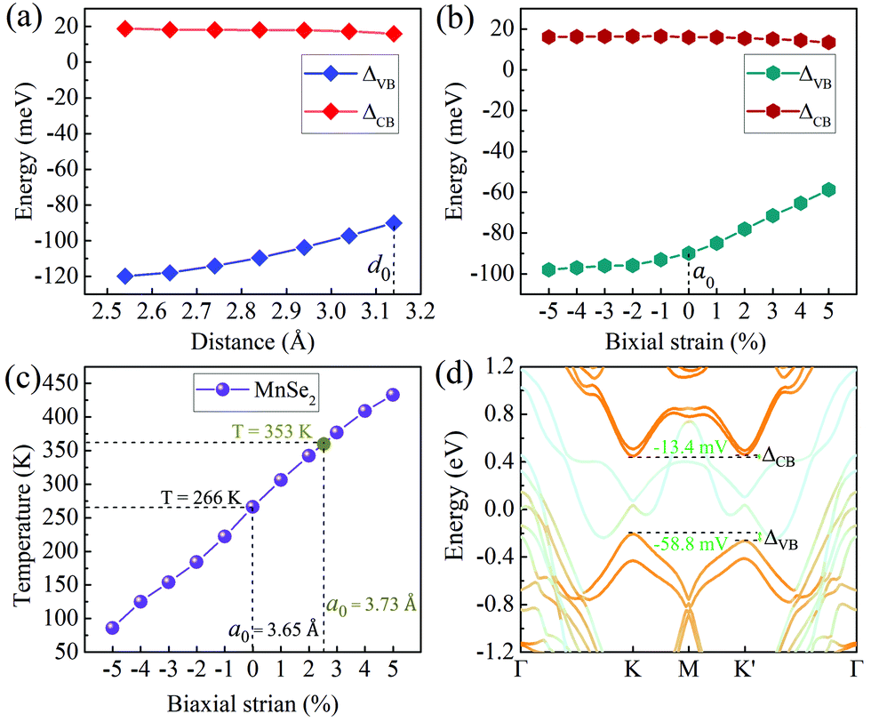 | ||
| Fig. 4 (a and b) valley-splitting changes versus interlayer distance and biaxial strain, respectively. (c) Curie temperatures changes versus biaxial strain of monolayer MnSe2. (d) Band structure of MoTe2/MnSe2 under 5% tensile strain. | ||
The in-plane stress is also an effective way to manipulate the electronic properties of heterojunctions, which can be achieved experimentally by stretching or bending the substrate.45Fig. 4(b) shows the change in the valley splitting size with biaxial stress regulation. Obviously, the application of biaxial compressive strain will increase the total valley splitting ΔKK′, but such an effect is not significant. When the compressive strain increases to 5%, ΔKK′ increases only by 10 meV. In contrast, the biaxial tensile strain will decrease ΔKK′, and when the tensile strain is 5%, ΔKK′ decreases by 33.8 meV, but it still has a large value of 72.2 meV, see Fig. 4(d). This result not only shows that biaxial strain can adjust the valley splitting, but also indicates that the intrinsic large valley splitting of the heterobilayer will have good stability for practical applications. For example, it has good tolerance for the splitting changes due to the lattice changes caused by thermal expansion and contraction. Note that although the DFT calculation is based on zero temperature, the results in this work are helpful and instructive to the experiment. Moreover, our DFT + MC calculations46 show that monolayer MnSe2 has a high intrinsic Curie temperature of 260 K (see Table S2 and Fig. S3 in the ESI† for details),40 consistent well with that near room-temperature reported by previous works.35–37 and it increases linearly with biaxial strain. When the tensile strain is 2.3% (this lattice constant value corresponds exactly to 5% tensile strains in the heterobilayer), the corresponding temperature increases from the intrinsic value of 266 K to 353 K, and it can be further increased to 443 K under 5% strains, much higher than room temperature [see Fig. 4(c)], which means that MnSe2 is of practical significance as a magnetic substrate to induce valley splitting.
Conclusions
In conclusion, we have performed first-principles and Berry curvature calculations to show that monolayer MnSe2 ferromagnetic metals can induce large valley splittings in MoTe2. The results show that the largest intrinsic total valley splitting of MoTe2 in the MoTe2/MnSe2 heterobilayer reaches a giant value of 106 meV, equivalent to the splitting size induced by an external magnetic field of 530 T. Both the application of vertical-stress and biaxial compressive strain regulation can further enlarge the valley splitting, which can be tuned to be as large as 138.6 meV by vertical-stress regulations. Although the biaxial tensile strains decrease the splitting, the magnitude can be maintained at tens of millielectron volts under appropriate tensile strains. Moreover, the DFT + MC simulations show that monolayer MnSe2 has an inherently high Curie temperature of about 266 K, and the temperature can be significantly increased by tensile strain, even reaching 443 K at 5% strain, much higher than room temperature. We expect that the giant valley splitting induced by the room-temperature ferromagnetic material will provide a new and excellent experimental candidate for the research of valleytronic devices.Computational method
First-principles calculations were performed using the Vienna ab initio simulation package (VASP).47 We approximated the exchange–correlation potential with the Perdew–Burke Ernzerhof (PBE) functional,48 and the ion–electron interaction is determined by the projector augmented wave (PAW) method.49 All the atoms of hybrid heterostructures were optimized until the total energies converged to below 1 × 10⁻⁵ eV, and the forces acting on the atoms were less than 0.01 eV Å−1. The plane wave energy cutoff was set to 500 eV, and the Monkhorst–Pack grids of the k-point mesh were set to 11 × 11 × 1. To avoid the interactions between periodic images, the vacuum space is set to no less than 18 Å. Spin–orbit coupling (SOC) and van der Waals interactions are taken into account to optimize the geometries and all subsequent calculations proposed by the DFT-D2 method.50 Considering the strong on-site Coulomb interaction for the d orbitals of the Mn atom,51 the GGA+Ueff method is used with a set of Ueff = 3.9 eV for Mn, which has been well tested by reports.35,36 The Berry curvature is calculated by employing the maximally localized Wannier-function (MLWF) method implemented in the WANNIER90 package.52,53 Ten d orbitals of the Mo and Mn atoms and six p orbitals of each Te and Se atoms are selected as the initial orbital projections, and a 19 × 19 × 1 uniform k grid is used for the construction of maximally localized Wannier functions. The difference in the spread of the total Wannier functions between two successive iterations converges to 10 × 10−10 Å2 within 500 iterative steps.Conflicts of interest
There are no conflicts to declare.Acknowledgements
This work was supported by the National Natural Science Foundation of China through Grants Nos. 12074112, 12104516, and 11674090, and by the Hunan Provincial Natural Science Foundation of China (Grant No. 2019JJ40029).Notes and references
- D. Xiao, M.-C. Chang and Q. Niu, Rev. Mod. Phys., 2010, 82, 1959 CrossRef CAS.
- J. R. Schaibley, H. Yu, G. Clark, P. Rivera, J. S. Ross, K. L. Seyler, W. Yao and X. Xu, Nat. Rev. Mater., 2016, 1, 16055 CrossRef CAS.
- Y. S. Ang, S. A. Yang, C. Zhang, Z. Ma and L. K. Ang, Phys. Rev. B, 2017, 96, 245410 CrossRef.
- D. Xiao, G.-B. Liu, W. Feng, X. Xu and W. Yao, Phys. Rev. Lett., 2012, 108, 196802 CrossRef PubMed.
- K. F. Mak, K. L. McGill, J. Park and P. L. McEuen, Science, 2014, 344, 1489 CrossRef CAS PubMed.
- Y. Li, J. Ludwig, T. Low, A. Chernikov, X. Cui, G. Arefe, Y. D. Kim, A. M. Van Der Zande, A. Rigosi and H. M. Hill, et al. , Phys. Rev. Lett., 2014, 113, 266804 CrossRef PubMed.
- A. Srivastava, M. Sidler, A. V. Allain, D. S. Lembke, A. Kis and A. Imamoğlu, Nat. Phys., 2015, 11, 141 Search PubMed.
- K. F. Mak, K. He, J. Shan and T. F. Heinz, Nat. Nanotechnol., 2012, 7, 494 CrossRef CAS PubMed.
- H. Zeng, J. Dai, W. Yao, D. Xiao and X. Cui, Nat. Nanotechnol., 2012, 7, 490 CrossRef CAS PubMed.
- G. Aivazian, Z. Gong, A. M. Jones, R.-L. Chu, J. Yan, D. G. Mandrus, C. Zhang, D. Cobden, W. Yao and X. Xu, Nat. Phys., 2015, 11, 148 Search PubMed.
- D. MacNeill, C. Heikes, K. F. Mak, Z. Anderson, A. Kormanyos, V. Zolyomi, J. Park and D. C. Ralph, Phys. Rev. Lett., 2015, 114, 037401 CrossRef CAS PubMed.
- J. Li, L. Gu and R. Wu, Phys. Rev. B, 2020, 101, 024412 CrossRef CAS.
- N. Singh and U. Schwingenschlögl, Adv. Mater., 2017, 29, 1600970 CrossRef PubMed.
- J. Zhou, J. Lin, H. Sims, C. Jiang, C. Cong, J. A. Brehm, Z. Zhang, L. Niu, Y. Chen and Y. Zhou, et al. , Adv. Mater., 2020, 32, 1906536 CrossRef CAS PubMed.
- S. Guo, Y. Wang, C. Wang, Z. Tang and J. Zhang, Phys. Rev. B, 2017, 96, 245305 CrossRef.
- J. Qi, X. Li, Q. Niu and J. Feng, Phys. Rev. B: Condens. Matter Mater. Phys., 2015, 92, 121403(R) CrossRef.
- C. Zhao, T. Norden, P. Zhang, P. Zhao, Y. Cheng, F. Sun, J. P. Parry, P. Taheri, J. Wang and Y. Yang, et al. , Nat. Nanotechnol., 2017, 12, 757 CrossRef CAS PubMed.
- L. Xu, M. Yang, L. Shen, J. Zhou, T. Zhu and Y. P. Feng, Phys. Rev. B, 2018, 97, 041405 CrossRef CAS.
- T. Norden, C. Zhao, P. Zhang, R. Sabirianov, A. Petrou and H. Zeng, Nat. Commun., 2019, 10, 1 CrossRef CAS PubMed.
- D. Zhong, K. L. Seyler, X. Linpeng, R. Cheng, N. Sivadas, B. Huang, E. Schmidgall, T. Taniguchi, K. Watanabe and M. A. McGuire, et al. , Sci. Adv., 2017, 3, e1603113 CrossRef PubMed.
- Z. Zhang, X. Ni, H. Huang, L. Hu and F. Liu, Phys. Rev. B, 2019, 99, 115441 CrossRef CAS.
- Q. Li, K. Chen and L. Tang, Phys. Rev. Appl., 2020, 13, 014064 CrossRef CAS.
- C. Ke, Y. Wu, W. Yang, Z. Wu, C. Zhang, X. Li and J. Kang, Phys. Rev. B, 2019, 100, 195435 CrossRef CAS.
- A. Zhang, Z. Gong, Z. Zhu, A. Pan and M. Chen, Phys. Rev. B, 2020, 102, 155413 CrossRef CAS.
- I. Khan, B. Marfoua and J. Hong, npj 2D Mater. Appl., 2021, 5, 1 CrossRef.
- J. F. Sierra, J. Fabian, R. K. Kawakami, S. Roche and S. O. Valenzuela, Nat. Nanotechnol., 2021, 16, 856 CrossRef CAS PubMed.
- B. Huang, G. Clark, E. Navarro-Moratalla, D. R. Klein, R. Cheng, K. L. Seyler, D. Zhong, E. Schmidgall, M. A. McGuire and D. H. Cobden, et al. , Nature, 2017, 546, 270 CrossRef CAS PubMed.
- C. Gong, L. Li, Z. Li, H. Ji, A. Stern, Y. Xia, T. Cao, W. Bao, C. Wang and Y. Wang, et al. , Nature, 2017, 546, 265 CrossRef CAS PubMed.
- Y. Ye, J. Xiao, H. Wang, Z. Ye, H. Zhu, M. Zhao, Y. Wang, J. Zhao, X. Yin and X. Zhang, Nat. Nanotechnol., 2016, 11, 598 CrossRef CAS PubMed.
- D. Wu, L. Huang, P.-Z. Jia, X.-H. Cao, Z.-Q. Fan, W.-X. Zhou and K.-Q. Chen, Appl. Phys. Lett., 2021, 119, 063503 CrossRef CAS.
- N. Mounet, M. Gibertini, P. Schwaller, D. Campi, A. Merkys, A. Marrazzo, T. Sohier, I. E. Castelli, A. Cepellotti and G. Pizzi, et al. , Nat. Nanotechnol., 2018, 13, 246 CrossRef CAS PubMed.
- H. Ren, L. Zhang and G. Xiang, Appl. Phys. Lett., 2020, 116, 012401 CrossRef CAS.
- M. Gibertini, M. Koperski, A. Morpurgo and K. Novoselov, Nat. Nanotechnol., 2019, 14, 408 CrossRef CAS PubMed.
- B. Shabbir, M. Nadeem, Z. Dai, M. S. Fuhrer, Q.-K. Xue, X. Wang and Q. Bao, Appl. Phys. Rev., 2018, 5, 041105 Search PubMed.
- C. Ataca, H. Sahin and S. Ciraci, J. Phys. Chem. C, 2012, 116, 8983 CrossRef CAS.
- M. Kan, S. Adhikari and Q. Sun, Phys. Chem. Chem. Phys., 2014, 16, 4990 RSC.
- D. J. OHara, T. Zhu, A. H. Trout, A. S. Ahmed, Y. K. Luo, C. H. Lee, M. R. Brenner, S. Rajan, J. A. Gupta and D. W. McComb, et al. , Nano Lett., 2018, 18, 3125 CrossRef CAS PubMed.
- Q. Li, L. Tang, C. Zhang, D. Wang, Q.-J. Chen, Y.-X. Feng, L.-M. Tang and K.-Q. Chen, Appl. Phys. Lett., 2017, 111, 171602 CrossRef.
- S. Zhang, J. Wang, N. L. Torad, W. Xia, M. A. Aslam, Y. V. Kaneti, Z. Hou, Z. Ding, B. Da and A. Fatehmulla, et al. , Small, 2020, 16, 1901718 CrossRef CAS PubMed.
- See the ESI† for the band structure, the density of states, Curie temperature of monolayer MnSe2, and interfacial charge-density difference of MoTe2/MnSe2 heterobilayers with calculation details.
- G. Yang, J. Li, H. Ma, Y. Yang, C. Li, X. Mao and F. Yin, Phys. Rev. B, 2018, 98, 235419 CrossRef CAS.
- K. Zhang, L. Wang and X. Wu, Nanoscale, 2019, 11, 19536 RSC.
- I. Khan, B. Marfoua and J. Hong, npj 2D Mater. Appl., 2021, 5, 1 CrossRef.
- Z. Zhao, H. Zhang, H. Yuan, S. Wang, Y. Lin, Q. Zeng, G. Xu, Z. Liu, G. Solanki and K. Patel, et al. , Nat. Commun., 2015, 6, 1 Search PubMed.
- W. Wu, L. Wang, Y. Li, F. Zhang, L. Lin, S. Niu, D. Chenet, X. Zhang, Y. Hao and T. F. Heinz, et al. , Nature, 2014, 514, 470 CrossRef CAS PubMed.
- L. Liu, X. Ren, J. Xie, B. Cheng, W. Liu, T. An, H. Qin and J. Hu, Appl. Surf. Sci., 2019, 480, 300 CrossRef CAS.
- G. Kresse and J. Furthmüller, Phys. Rev. B: Condens. Matter Mater. Phys., 1996, 54, 11169 CrossRef CAS PubMed.
- J. P. Perdew, K. Burke and M. Ernzerhof, Phys. Rev. Lett., 1996, 77, 3865 CrossRef CAS PubMed.
- P. E. Blöchl, Phys. Rev. B: Condens. Matter Mater. Phys., 1994, 50, 17953 CrossRef PubMed.
- S. Grimme, J. Comput. Chem., 2006, 27, 1787 CrossRef CAS PubMed.
- I. Solovyev, P. Dederichs and V. Anisimov, Phys. Rev. B: Condens. Matter Mater. Phys., 1994, 50, 16861 CrossRef CAS PubMed.
- A. A. Mostofi, J. R. Yates, Y.-S. Lee, I. Souza, D. Vanderbilt and N. Marzari, Comput. Phys. Commun., 2008, 178, 685 CrossRef CAS.
- N. Marzari, A. A. Mostofi, J. R. Yates, I. Souza and D. Vanderbilt, Rev. Mod. Phys., 2012, 84, 1419 CrossRef CAS.
Footnote |
| † Electronic supplementary information (ESI) available: The band structure, density of states, Curie temperature of monolayer MnSe2, and interfacial charge-density difference of the MoTe2/MnSe2 heterobilayer with calculation details. See DOI: 10.1039/d1ma01196k |
| This journal is © The Royal Society of Chemistry 2022 |