
 Open Access Article
 This Open Access Article is licensed under a Creative Commons Attribution-Non Commercial 3.0 Unported Licence
Engineering chiral plasmonic nanostructures for gain-assisted plasmon amplification and tunable enhancement of circular dichroism†
Vikas
Yadav
and
Soumik
Siddhanta
 *
*
Department of Chemistry, Indian Institute of Technology Delhi, Hauz Khas, New Delhi – 110016, India. E-mail: soumik@iitd.ac.in
First published on 30th December 2021
Abstract
Circular dichroism (CD) from plasmonic nanostructures yields fascinating insights into their chiroptical properties; however, the weak signals make their investigations profoundly challenging. We have demonstrated a method for significantly improving the signal enhancement by introducing a gain medium on these single plasmonic nanoparticles and creating surface plasmon amplification of stimulated emission of radiation (SPASER). The chiral nanostructure, which consists of a single v-shaped gold nanorod dimer, showed a prominent plasmonic chiroptical response when excited with an obliquely incident beam of circularly polarized light. When the same gold nanorods were arranged in a twisted configuration, the response was intrinsically chiral irrespective of the angle of incidence. However, for both these classes of nanoparticle arrangement, the chiroptical response was enhanced by several orders of magnitude when a doped gain medium layer was introduced, and a significant enhancement in the anisotropy factor was observed when the gain coefficient reached a critical value of the lasing threshold. The chiroptical response could be efficiently tuned by changing the geometry of the nanoconstruct as well as the gain coefficient of the surrounding layer, thus demonstrating an alternative method for obtaining chiral plasmonic materials with remarkably high anisotropy factors.
Introduction
Chiral metamaterials have recently been shown to exhibit interesting electromagnetic properties due to disruption of their mirror symmetry, resulting in the emergence of artificial magnetism, a negative refractive index, and circular dichroism, among other features.1,2 In particular, there has been an increasing interest in studying the circular dichroism (CD) signals from these materials owing to their greater detectability compared with naturally chiral compounds.2 Such artificial chiral materials are being increasingly used in photonic devices,3 catalysis4 and in fabricating optical components and devices.5 Interestingly, the CD response can also be induced in achiral plasmonic nanoparticles when they are combined with chiral molecules.6 Particularly, in chiral-scaffold-assembled plasmonic nanoparticles, strong chiroptical effects can be observed, which can even be extended to achiral nanoparticle assemblies due to near-field coupling through chiral molecule layers.2 Despite considerable progress in the design of chiral nano-assemblies, it remains significantly challenging to strategize enhancements in chirality that can accentuate the chiroptical effects, thus limiting their application in molecular sensing and detection. Although the geometric modulation of several nanoparticle-based chiral assemblies has been studied in detail, systematic exploration of the integration of various optical modulation techniques is lacking. Further investigation of optical manipulation in such geometry-optimized nanostructures could lead to better predictive designs of CD-based sensitive optical devices.Some of the highest CD enhancements have been observed from chiral plasmonic nanoparticles,7 with plasmon-enhanced CD (PCD) spectroscopy displaying enhancements of five orders of magnitude from plasmonic super-chiral fields.8,9 Collinear arrangements of gold nanorods have been shown to possess two orders of PCD amplification, notably for molecules located in the plasmonic hotspots.10 In addition, dissymmetrical nanostructures with well-defined hotspots6,8,11,12 and linear, one-dimensional assembly that sustains plasmon propagation has also enabled the control of optical properties leading to significant enhancements in PCD.13,14 Even if the nanostructures are achiral, chirality can be induced upon illumination using a circularly polarized plane wave at an oblique incidence or an input vortex beam at normal incidence.15 Consequently, the PCD amplification obviates the use of a high concentration of chiral samples for a stable signal-to-noise ratio.16 Such amplification can also be harnessed by other optical spectroscopies such as surface-enhanced Raman spectroscopy (SERS) and super-resolution microscopies, which can provide detailed molecular information.17,18 SERS is highly dependent on the hotspot intensities, and when a chiral molecule is investigated it can lead to enhancement of the Raman optical activity.19 However, the design of nanoaggregates can alter the polarization of Raman-scattered light, making it challenging to control the molecular attachment sites in the aggregates, which can lead to irreproducible enhancements.20 Therefore, it is imperative to strategize or explore alternative nanoparticle designs for signal enhancement that does not rely on super-chiral aggregates of nanostructures formed through physical or chemical routes.
In this paper, we have proposed an alternative method for enhancing the chiroptical response from plasmonic nanoparticle systems by introducing a gain medium surrounding the nanoconstruct.21 Recently, it has been reported that significant amplification takes place when such a gain medium is introduced in the nanostructures through a phenomenon known as surface plasmon amplification by the stimulated emission of radiation (SPASER).22 In essence, the gain medium amplifies the plasmon-resonance-mediated light amplification, which has been demonstrated by multiple groups experimentally.23 Theoretical calculations have shown several orders of magnitude amplification of light gain through SPR, specifically in concentric core–shell nanostructures.24 Typically, a dye-doped shell over an engineered nanostructure can form a SPASER-based nano-laser.24 Wavelength tunability and polarization sensitivity for such systems has also been realized along with the generation of a coherent high-intensity field that is far beyond the diffraction limit.25 We have theoretically investigated the effect of the SPASER configuration on plasmonic chiral nano-assemblies such as gold nanorod dimers (dimer-1), which show a PCD response when circularly polarized light is obliquely incident. We further extended the calculations to include the twisted configuration of gold nanorods, which shows intrinsic chirality in the solution phase (dimer-2). In both cases, a remarkable increase in chiral response from the dimer was observed when the gain coefficient was increased, concurrent with the observation of super resonances. We have simulated the far-field and near-field properties of such systems and have demonstrated, for the first time, a strategy to control the chiral properties of plasmonic assemblies through gain-induced amplification. These attributes make our strategy a promising candidate for ultra-sensing, specifically in the field of biology and medicine where this property can be harnessed for scanning near-field optical microscopy and for building high-performance molecular sensors and photodetectors.26,27
Materials and methods
Simulation parameters
The simulations were performed using the Lumerical FDTD solutions suite.28 For the dielectric properties of gold nanorods, the model of Johnson and Christy29 was used; and for silica, which constitutes the glass coating, the Palik model was employed. For the surrounding medium, a refractive index of 1.33 was used to represent water as a solvent. For each simulation, a mesh size of about 0.5 nm and a perfectly matched layer boundary condition was used to avoid any kind of long-range ordering. The simulation was performed at a temperature of 300 K, and a typical simulation time of about 100 fs was used. To simulate the chiroptical response, right and left circularly polarized light was incident on the nanostructure and the CD curve was plotted as the difference in scattering between the two.Structural parameters
Gold nanorods with an aspect ratio of 1![[thin space (1/6-em)]](https://www.rsc.org/images/entities/char_2009.gif) :3 (diameter:length) were initially chosen for the simulations. Similar configurations were used for both dimer-1 and dimer-2. To characterize the angular dependence of the PCD signals, the three possible angular variations (θ, ϕ, and δ) were simulated. The aspect ratio of the nanorods was also varied to observe the changes in the PCD signals. The structure was suspended in water as a medium to mimic the experimental conditions. For observing the effect of the gain medium on the PCD signal, the thickness of the doped silica layer was varied from 0 nm to 25 nm. The real part of the refractive index was fixed at a value of 1.5, and the imaginary part was varied from 0.01 to 0.2. Circularly polarized light (CPL) was incident from the Z-axis, at an angle phi (ϕ) with the YZ plane that passes through the dimer. The amplitude of the light was taken to be unity, and the PCD response was obtained from 400 nm to 1100 nm.
:3 (diameter:length) were initially chosen for the simulations. Similar configurations were used for both dimer-1 and dimer-2. To characterize the angular dependence of the PCD signals, the three possible angular variations (θ, ϕ, and δ) were simulated. The aspect ratio of the nanorods was also varied to observe the changes in the PCD signals. The structure was suspended in water as a medium to mimic the experimental conditions. For observing the effect of the gain medium on the PCD signal, the thickness of the doped silica layer was varied from 0 nm to 25 nm. The real part of the refractive index was fixed at a value of 1.5, and the imaginary part was varied from 0.01 to 0.2. Circularly polarized light (CPL) was incident from the Z-axis, at an angle phi (ϕ) with the YZ plane that passes through the dimer. The amplitude of the light was taken to be unity, and the PCD response was obtained from 400 nm to 1100 nm.
Results and discussion
Extrinsic and intrinsic chiralities of the gold nanorod dimers
The schematic of our simulations that represents our active nanosystem is shown in Fig. 1A. Two gold nanorods are placed in a v-shaped configuration and serve as an achiral structure with a symmetrical geometry (dimer-1). However, the chirality arises due to symmetry breaking by the oblique angle of incidence of the circularly polarized light.30 Such extrinsic chirality associated with assemblies of gold nanorods has been demonstrated earlier.30 The choice for the gold nanorod dimer is also influenced by the fact that these dimer geometries can be controlled experimentally and can also be fabricated using a bottom-up or top-down approach.31 As shown in Fig. 1, the chirality is manifested as a difference in the scattering cross-section of right circularly polarized light (RCP; red) and left circularly polarized light (LCP; black), respectively (Fig. 1B and C). The whole arrangement becomes chiral, which cannot be superimposed on its mirror image, and gives rise to a geometrically initiated extrinsic chiral system. The CD spectra, which are essentially the difference between the scattering of differently polarized light, takes a bisignate form (Fig. 2). | ||
| Fig. 1 (A) The simulation setup showing the gold nanorod dimer (dimer-1) and the obliquely incident circularly polarized light (CPL). The gold nanorods are coated with a gain medium of doped silica, and the entire simulation is performed in water as a medium. (B) The computed scattering responses of the uncoated gold dimer to LCP and RCP light are shown in black and red, respectively. (C) The computed scattering responses of the gold dimer coated with 5 nm silica to LCP and RCP light are shown in black and red, respectively. (D) Plasmonic hybridization of the gold nanorod dimers. The black and red curves correspond to the uncoated and the 5 nm coated nanorods interacting with LCP light. (E) The energy level diagram corresponding to (D) describing the interaction between the plasmonic modes (ω0), resulting in a bonding (ω−) and an anti-bonding mode (ω+), respectively. The bonding mode redshifts to 1.59 eV and the anti-bonding mode blue shifts to 1.77 eV for the uncoated nanorods (black). Similar shifts have also been observed for 5 nm silica coated nanorods (in red). (F) The asymmetric and symmetric modes (bonding and anti-bonding modes, respectively) shown as charge density distributions. The anti-bonding and bonding modes for uncoated gold nanorods are shown in (i and ii) and for 5 nm coated gold nanorods in (iii and iv). These modes are calculated for LCP light with an oblique incidence of 60° with the y–z axis. | ||
 | ||
| Fig. 2 Circular dichroism spectra of dimer-1 emerging from the difference between the scattering of LCP (black) and RCP (red) light (A) giving rise to a bisignate form of the spectrum (B). | ||
After right hand circularly polarized (RCP) and left hand circularly polarized (LCP) light were incident on the uncoated gold nanorod dimers, two peaks were obtained at around 709 nm and 774 nm (Fig. 1B), which corresponds to plasmonic hybridization that gives rise to the antibonding and bonding modes, respectively.30 The two plasmonic modes interact with the RCP and LCP differently and give rise to the difference in the scattering from the two nanorods, while inducing a strong coupling with the obliquely incident light. In addition to the stronger longitudinal modes, their plasmonic coupling also gives rise to a very weak transverse mode at around 500 nm. The longitudinal mode is responsible for the extrinsic chirality of the system, which is different for LCP and RCP light and gives rise to the PCD spectrum. As seen in Fig. 1D, when the two nanorods are placed in close proximity, the resulting two peaks from the plasmonic resonance of the gold nanorods with a silica shell of 5 nm are red-shifted by 9 nm and 13 nm (for anti-bonding and bonding modes, respectively) due to the dielectric medium dependence.32 The plasmonic state of the nanorods can be seen as dipole moments in the frequency domain oriented along the individual nanorod axes, giving rise to a resultant dipole that can be decomposed into symmetric and anti-symmetric components. When the two dipoles of the nanorods oscillate in phase, it is essentially a bonding mode, which occurs at a lower hybridized energy (ω−) level, whereas the anti-bonding dipoles oscillate in an anti-phase and is located at a higher hybridized energy (ω+) level (Fig. 1F). The excitation wavelength can excite either of the symmetric or anti-symmetric modes of the dipole orientations, and its overlap with the evolution of the electric field vectors’ can give rise to either favourable or unfavourable interactions with the two nanorods, resulting in the emergence of the PCD spectrum.
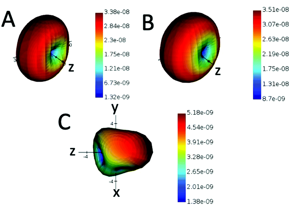
The hybridized modes are also reflected in the near-field intensity distribution of the gold nanorod dimer (Fig. 3). The electric field intensities are greater for bonding modes than the anti-bonding modes. At an angle of 60 degrees, the bonding mode shows an electric field enhancement (|E|/|E0|)4 of the order of 109. The localized SPR (LSPR) peaks from the gold nanorods or rather any plasmonic nanostructures, which are usually probed via electron energy loss spectroscopy, are the results of the eigenstates of the surface charge oscillations that are coherent in nature.33 Single nanoparticle structures such as the v-shaped gold nanorods have a much simpler and easily identifiable set of LSPR peaks as the higher-order plasmonic eigenstates are mostly degenerate or have a dark mode with the net dipole moment as zero. The Fano-type shape profiles obtained from these scattering geometries can be harnessed for several applications. The hotspots arising between the nanorods and also the larger cross-section as compared with the spherical nanoparticles have been proved to be a good enhancer for SERS in the visible range.34 The lineshape and linewidth of the PCD spectrum can be elucidated from the far-field properties. The calculated far-field profiles in Fig. 4 show a doughnut shape that is a signature of a point dipole, particularly at hybridized frequencies (Fig. 4A and B), which also implies that the resultant of the two dipoles from the nanorods is a single dipole. However, at other frequencies (Fig. 4C), the far-field scattering profile is no longer a perfect doughnut-shaped but is distorted, which results in the loss of the point dipole nature. Such a distortion arises from a mixture of the different hybridized states. Similar behavior is observed in case of RCP light. We also see a doughnut shape at hybridized frequencies (Fig. S1A and B, ESI†). However, when other frequencies are used, a distortion is observed (Fig. S1C, ESI†). Therefore, in order to maintain a perfect dipole response and narrow lineshapes, excitation at the hybridized states is preferred over other frequencies.
 | ||
| Fig. 3 Calculated pattern of near-field intensity of the gold nanorod dimer-1: (A and B) the near-field intensities when the uncoated and 5 nm silica coated nanostructures are excited by LCP light at their specific bonding wavelengths (774 and 787 nm), respectively; and (C and D) the near-field intensities when the uncoated and 5 nm silica coated nanostructures are excited by LCP light at their respective anti-bonding wavelengths (709 and 718 nm), respectively. | ||
 | ||
| Fig. 4 Calculated far-field profiles of the gold nanorod dimer-1. (A) Dimer excited by LCP light at the anti-bonding wavelength of 709 nm, and at the bonding wavelength of 774 nm (B). (C) Off-resonance excitation at 650 nm of the gold nanorod dimer. | ||
Another class of gold nanodimers (dimer-2) with intrinsic chirality was also explored. The chirality arises from the small dihedral angles between them, and the twisted configuration of one nanorod versus the other one breaks the centrosymmetric nature of the dimer assembly.35 The CD spectrum shows a similar bisignate form (Fig. S2, ESI†), which is maintained at all angles of incidence unlike the dimer-1 configuration. The far-field profiles at the bonding frequencies show doughnut-shaped profile, indicative of the formation of a single dipole like the dimer-1 configuration. It is interesting to note that the far-field properties are similar when the angle of incidence is changed (Fig. S6 and S7, ESI†).
Chiral amplification in gain-assisted gold nanorod dimers
We have been motivated to design a SPASER (surface plasmon amplification by the stimulated emission of radiation) type of configuration to study its effect on the enhancement of the extrinsic chirality of the gold nanorod dimer. A remarkable property of the SPASER configuration is the strong surface plasmon resonance (SPR) amplification and compression of the SPR linewidth.36 According to this concept, a gain medium is introduced on the gold nanorods, which transfers the energy to the localized SPR of the metal. These surface plasmons stimulate transitions in the gain medium, further stimulating the surface plasmons in the same range of frequencies. The photon–plasmon coupling taking place is like resonance in a nanocavity, and the quality factor determines the output optical properties.37 Thus, in such a configuration, the realization of a single nanoparticle nano-laser can be technically realized. Our aim is to harness this enhanced optical output with additionally induced chiroptical properties.For the simulations, the nanoparticle assembly (for both dimer-1 and dimer-2) was assumed to be in water with a refractive index of 1.33. A gain medium was introduced around the gold nanorod dimer in the form of a doped silica layer with a refractive index of nshell = 1.5 − ik, where k is the gain coefficient and is connected to the amplification of light coefficient.24 This gain coefficient was introduced to account for the relevant light–medium interaction. The use of silica coating is preferred as it can be easily realized experimentally through the incorporation of dye molecules.24 In order to determine the strength of light–particle interactions, the anisotropy factor g was introduced, which is given by the formula:38

As discussed previously, the longitudinal scattering is more dominant in the gold nanorod assembly than its dipolar counterpart. For dimer-1, initially, when k = 0, the optical cross-section of the absorbance, Cabs, is greater than that of the scattering, Cscat, indicating that the absorbance by the particle is dominant (Fig. 5A). However, when the gain medium is introduced and k > 0, Cscat increases till it reaches a critical point (k = 0.104) (Fig. 5B). At the critical point (where the optical cross-section of extinction, Cext ∼ 0), the scattering cross-section reaches an extreme value around 100 times more than its value at k = 0 (Fig. 5C). The absorption of light at this point has a negative value, which indicates a net amplification that happens due to compensation of the absorption of light by the gain medium. At this critical point, the strength of the SPR is maximally amplified by the energy transfer from the gain medium, and any further increase in the value of k leads to energy dissipation and breakdown of the SPASER system. This is an important property of spasing, where the nanoparticle system is turned from a dissipative system to a strongly amplifying one at the critical point. The calculated anisotropy factor values, which are a direct indicator of the PCD response, also showed a similar trend and peaked at the critical point (Fig. 5D). A maximum value of 1.045 of the g-factor for the gold nanorod dimer was achieved, which is orders of magnitude greater than other gold nanorod-based structures, which typically have g-values of around 10−3.40 When k is varied, the scattering cross-section, Cscat, increases at first till a particular value and then decreases, which is again reflected through the g values (Fig. 5D). Experimentally, the PCD is only half of this scattering, and the discrimination of the actual CD from the differential scattering is calculated through the Mueller matrix of the scattering of the gold nanorod dimer arrangement, which has been reported by Lu et al.30 The anisotropic factor and hence the chiral response also varies with the wavelength of the incident light, and we see a maximum at the bonding wavelength and a minimum at the anti-bonding wavelength (Fig. 5E). The high g values of the gold nanorod system can be attributed to the supressed interband damping due to low SPR energy owing to its high aspect ratio41 and also the drastic reduction of plasmon dephasing and high light-scattering efficiency, which makes the threshold for the surrounding gain media much lower than expected.
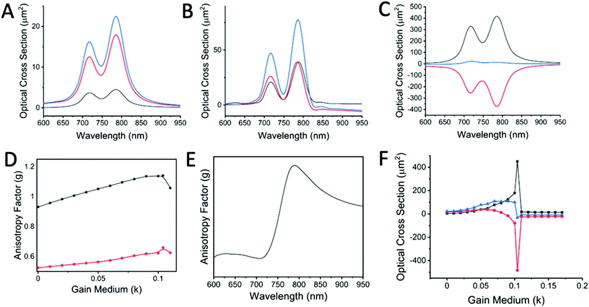 | ||
| Fig. 5 (A–C) Calculated absorbance (red), scattering (black) and extinction (blue) of a gold nanorod dimer system immersed in water and with LCP light incident at an oblique angle of incidence on dimer-1: for systems with k values of 0 (A), 0.05 (B) and 0.104 (C). (D) Calculated anisotropy factor (g) with different k values, where the black and red curves show the trend for the bonding and anti-bonding modes, respectively. (E) Calculated anisotropy factors as a function of different wavelengths. (F) Calculated optical cross-section (absorbance (red), scattering (black) and extinction (blue)) as a function of different k-values around the critical point of 0.104. | ||
The change of k values and the resultant optical properties show the physical implications of the lasing phenomenon. When the LCP or RCP light at a resonant wavelength with the bonding mode is obliquely incident, the critical point is reached when k = 0.104. At this k value, the sharp resonance can be seen in Fig. 5F. The extinction value jumps to a high value and drops to below 0 at the close vicinity of the critical point. However, unlike SPASERs, the PCD or the scattering line profile is not sharp, and this can be understood from the far-field profiles at the critical value of k. At any other frequencies that are different from the resonances, we again obtain a mixed state, as seen from the far-field scattering plots (Fig. S3 and S4, ESI†). The presence of such mixed states prevents the PCD spectra from having sharp line profiles. The PCD phenomenon is also the direct result of the near-field interference excited by the orthogonally polarized incident light.16 The local field is the sum of the incident field and the scattered fields from the particles. The near-field intensity at the critical point is around 3 times greater than the system in which the gain medium is absent (Fig. S5, ESI†). The maximum intensity spots lie at the end of the nanorods and at the connection between the nanorods, specifically when the coating is very thin (<5 nm) due to the formation of plasmonic “hotspots”. Hence, for the gold nanorod dimer assembly, the plasmonic near-field amplification is manifested as the increase in the CD signal and, consequently, the anisotropy factor (g) at the critical point.
For the dimer-2 configuration, the gold nanorods are in a twisted configuration with an angle of 80° between the long axes (Fig. 9A) and the light is incident at a right angle to the nanoparticles (a condition in which the extrinsically chiral system shows no chirality). A silica coating of 5 nm was introduced with varying k-values to account for the gain medium. Fig. 9B and C show the variation in absorbance, scattering and extinction with k values of 0, 0.07 and 0.150. The anisotropic or g-factor shows a peak at the k value of 0.150 and is found to be higher for the bonding frequencies compared with the anti-bonding ones at the optimum k-values. However, it is worthy of note that the difference in g-factors for the antibonding and bonding frequencies is much less than that observed in the case of extrinsically chiral systems. In other words, for systems with intrinsic chirality, the g-factor values are higher in even anti-bonding frequencies. For our system we observe that the critical value of k is found at 0.150. However, it is advisable to use the bonding frequencies for both incident LCP and RCP light, since they act as single dipoles (indicated by a doughnut shape), as opposed to a distorted shape when anti-bonding frequencies are used (Fig. S6 and S7, ESI†). Since the nanoparticle dimers are intrinsically chiral, we observed the same trend in the calculations for an angle of incidence of 60° (Fig. S10, ESI†). It is important to note that these simulations were done in water to mimic the actual experimental conditions. In this case the g-values were calculated as:

Tuning of chirality enhancement of the gold nanorod dimer
The chiroptical behaviour of the gold nanorod dimer is highly tunable and depends on the dimer's architecture, including the thickness of the gain medium. It is evident that the introduction of various gain medium thicknesses alters the chiroptical response, resulting in varying anisotropic factor (g) values, which were found to increase till 5 nm of gain medium layer was reached and gradually decreased with increasing thickness (Fig. 6). Also, with an increasing thickness, the bonding and the antibonding modes tend to move closer to each other (Fig. 6A). The change of the gain coefficient, k, also results in a differential chiroptical response for different thicknesses (Fig. 6B). The electric field intensities in the presence and absence of the gain medium for both bonding and anti-bonding modes show a similar trend to the anisotropy factor with higher g values at 5 nm thickness for the 1:3 aspect ratio of the gold nanorods. Another important factor affecting the chiroptical response is the geometry of the dimer itself. Fig. 7 shows the variation of the angle between the two nanorods and the resulting chiroptical response. When the gold nanorod dimers are parallel or in the same plane as the incident beam, they are achiral. This can be seen by the variation of the anisotropic factor, g. The corresponding near-field intensities are shown in Fig. 7B. In the case of the chiral response, the differential interaction of the LCP and RCP with the gold nanorod dimer occurs as the dipole orientation of the LCP electric field vectors either matches well with the symmetric or anti-symmetric mode and vice versa for the RCP electric field vectors. From the angular variation of the incident circularly polarized light and also the angle between the nanorods, the differential interaction, and hence the resultant PCD intensities, reach maximum values at ϕ = 45, θ = 90 and δ = 0, 180 and 360°, respectively (Fig. S11, ESI†). Under these conditions, the dipoles of the dimer and the spatial electric field vectors of the circularly polarized light overlap favourably, whereas at ϕ = 0, θ = 0 and δ = 90 and 270°, these overlaps do not occur, and the extrinsic chiral activity cannot be seen as the CD signals take the form of a single gold nanorod. The angle ϕ is essentially the change in the angle of incidence of light on the nanorods, which plays a big role in the enhancement. These results suggest that the induced extrinsic chirality is dependent on the dimer organization.
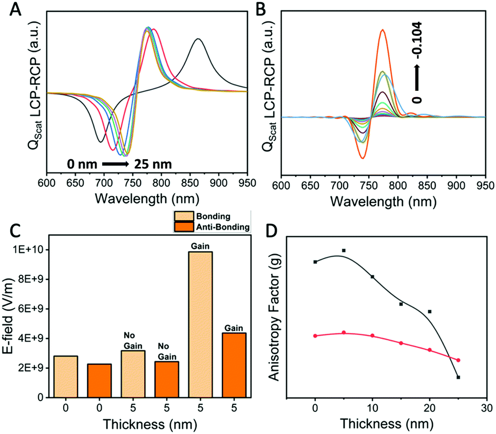 | ||
| Fig. 6 (A) PCD spectra at different silica layer thicknesses on dimer-1 without a gain medium. (B) PCD spectra of the gold nanorod dimer with a 15 nm silica thickness containing different values of the gain coefficient k. (C) Variation of the E-field with various thicknesses of silica with and without a gain medium. The E-field is calculated from the obliquely incident LCP light on the gold nanoparticle dimer at the bonding and anti-bonding resonances, respectively. (D) Variation of the anisotropic factor (g) for both bonding (black) and anti-bonding (red) modes with the thickness of the gain medium. | ||
 | ||
| Fig. 7 (A) Variation of the chiroptical response of the gold nanorod dimer-1 with the angle between the two nanorods. (B) Variation of the E-field intensity with the angle, and (C) the corresponding CD signals. (D) Variation of the anisotropic factor (g) with varying value of angle θ for both bonding (black) and anti-bonding modes (red). | ||
On changing the aspect ratio of the nanorod, the efficiency or the g values also undergo changes, as shown in Fig. 8. Even with similar aspect ratios, the gold nanorod system has different g values, which ultimately depend on the overall configuration of the dimers. In the case of the 1:3 aspect ratio, a higher length/height gave a greater g value. Interestingly, this value was even more than that of 1:4 aspect ratio nanorods with a higher length/height (Fig. 8B). It is generally seen that larger g values are associated with nanostructures with greater aspect ratios for a wavelength regime where scattering is predominant, and the higher-order multipoles of these nanorods are expected to contribute significantly. The structures with high g values, such as with gold nanorods, consist of the helical movement of displacement currents in the nanostructures, which are the result of interactions with the circularly polarized light. These PCD signals are further enhanced when the nanorods touch each other due to the enhanced charge-transfer plasmon.42 Even if there is a gap that is induced by the gain medium, there is a specific volume in which strong near-field coupling occurs. The anisotropic shape of the nanorod system also ensures less damping of the plasmons and certainly much less than its spherical counterpart. The ability to vary the g-factor through the angles and the aspect ratio enables a higher degree of tunability in these nanostructures. These promising results of the numerical simulations are expected to stimulate interest in experimental studies for the incorporation of the SPASER principle for obtaining a strong chiroptical response from plasmonic nanomaterials and other areas including the extension of exciton-coupling theory to plasmonics and probing the dark modes with extremely low radiative losses that can be harnessed for interesting applications of plasmonic metamaterials.
 | ||
| Fig. 8 (A) Variation of the PCD response of dimer-1 with the aspect ratio: the blue and red curves are PCD from the gold nanorod dimer having same aspect ratios (1:3) but different lengths; and the black curve corresponds to the PCD from dimers with a 1:4 aspect ratio. (B) Anisotropy factors for the corresponding dimer diameter (D) and height (H) values. | ||
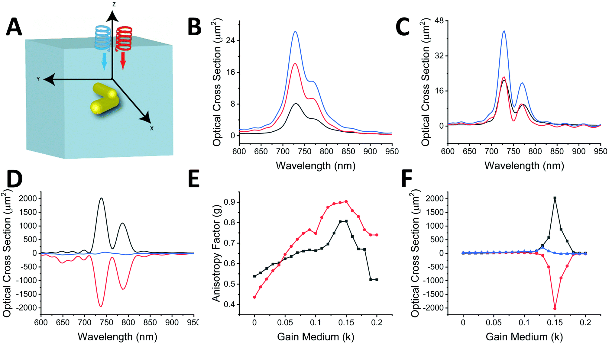 | ||
| Fig. 9 (A) The simulation setup showing the twisted gold nanorod assembly showing intrinsic chirality (dimer-2). Figures (B–D) represents absorbance, scattering and extinction of nanorod systems with k values of 0, 0.07 and 0.150 respectively. Calculated absorbance (red), scattering (black) and extinction (blue) are shown for a gold nanorod dimer system immersed in water and with left circularly polarized light incident at normal incidence. (E) The calculated anisotropy factor (g) with different k values. The black and red curves show the trend of bonding and anti-bonding modes respectively. (F) The calculated optical cross-section as a function of different values of k-values around the critical point of 0.150. | ||
Conclusions
In summary, we have demonstrated a new method for enhancing the anisotropic factor, g, of the plasmonic chiroptical nanostructure to remarkably high values. The extrinsically chiral system, which consists of v-shaped gold nanorods, shows a typical g-value of 0.4, but when a gain medium is introduced, and the gain coefficient is adjusted such that the absorbance reaches a negative value and the optical extinction cross-section almost reaches zero, the g-value reached a value of over 1. Similar behavior is also seen in the case of twisted nanorod dimers with intrinsic chirality. This enhanced g-value also coincides with the single-particle lasing regime akin to a SPASER configuration where system seems to amplify light although scattering is high in all directions. The chiral enhancement is tunable and is dependent upon the geometry of the nanorods as well as the angle of incidence of the circularly polarized light. The demonstrated nanostructures and the chiral enhancement method through the introduction of the principles of SPASER can play key roles in highly sensitive single-molecule chiroptical spectroscopic sensing and imaging.Conflicts of interest
There are no conflicts to declare.Acknowledgements
This work was supported by the IIT Delhi SEED grant (IITD/Plg/Budget/2020-2021/204758) and DST SERB (SRG/2020/000440). Vikas Yadav thanks UGC, Govt. of India for the student fellowship.Notes and references
- S. Yoo and Q.-H. Park, Nanophotonics, 2019, 8, 249–261 Search PubMed.
- Z. Y. Bao, J. Dai, Q. Zhang, K. H. Ho, S. Li, C. H. Chan, W. Zhang and D. Y. Lei, Nanoscale, 2018, 10, 19684–19691 RSC.
- A. Potts, A. Papakostas, N. Zheludev, H. Coles, R. Greef and D. Bagnall, J. Mater. Sci.: Mater. Electron., 2003, 14, 393–395 CrossRef CAS.
- Y. Luo, C. Chi, M. Jiang, R. Li, S. Zu, Y. Li and Z. Fang, Adv. Opt. Mater., 2017, 5, 1700040 CrossRef.
- X. Wu, C. Hao, L. Xu, H. Kuang and C. Xu, Small, 2020, 16, 1905734 CrossRef CAS PubMed.
- N. A. Abdulrahman, Z. Fan, T. Tonooka, S. M. Kelly, N. Gadegaard, E. Hendry, A. O. Govorov and M. Kadodwala, Nano Lett., 2012, 12, 977–983 CrossRef CAS PubMed.
- I. Lieberman, G. Shemer, T. Fried, E. M. Kosower and G. Markovich, Angew. Chem., 2008, 120, 4933–4935 CrossRef.
- M. L. Nesterov, X. Yin, M. Schäferling, H. Giessen and T. Weiss, ACS Photonics, 2016, 3, 578–583 CrossRef CAS.
- Y. Tang and A. E. Cohen, Science, 2011, 332, 333–336 CrossRef CAS PubMed.
- Z. Zhu, W. Liu, Z. Li, B. Han, Y. Zhou, Y. Gao and Z. Tang, ACS Nano, 2012, 6, 2326–2332 CrossRef CAS PubMed.
- B. M. Maoz, R. van der Weegen, Z. Fan, A. O. Govorov, G. Ellestad, N. Berova, E. Meijer and G. Markovich, J. Am. Chem. Soc., 2012, 134, 17807–17813 CrossRef CAS PubMed.
- F. Lu, Y. Tian, M. Liu, D. Su, H. Zhang, A. O. Govorov and O. Gang, Nano Lett., 2013, 13, 3145–3151 CrossRef CAS PubMed.
- X. Wu, L. Xu, W. Ma, L. Liu, H. Kuang, W. Yan, L. Wang and C. Xu, Adv. Funct. Mater., 2015, 25, 850–854 CrossRef CAS.
- Y. Zhao, L. Xu, W. Ma, L. Wang, H. Kuang, C. Xu and N. A. Kotov, Nano Lett., 2014, 14, 3908–3913 CrossRef CAS PubMed.
- X. Wang and Z. Tang, Small, 2017, 13, 1601115 CrossRef PubMed.
- H. Wang, Z. Li, H. Zhang, P. Wang and S. Wen, Sci. Rep., 2015, 5, 1–6 CAS.
- S. Siddhanta, V. Thakur, C. Narayana and S. Shivaprasad, ACS Appl. Mater. Interfaces, 2012, 4, 5807–5812 CrossRef CAS PubMed.
- F. Wei, D. Lu, H. Shen, W. Wan, J. L. Ponsetto, E. Huang and Z. Liu, Nano Lett., 2014, 14, 4634–4639 CrossRef CAS PubMed.
- M. Das, D. Gangopadhyay, J. Šebestík, L. Habartová, P. Michal, J. Kapitán and P. Bouř, Chem. Commun., 2021, 57, 6388–6391 RSC.
- P. A. Mosier-Boss, Nanomaterials, 2017, 7, 142 CrossRef PubMed.
- M. I. Stockman, Phys. Rev. Lett., 2011, 106, 156802 CrossRef PubMed.
- M. Noginov, G. Zhu, A. Belgrave, R. Bakker, V. Shalaev, E. Narimanov, S. Stout, E. Herz, T. Suteewong and U. Wiesner, Nature, 2009, 460, 1110–1112 CrossRef CAS PubMed.
- J.-H. Wang, Z. Gao, P. Song, P. N. Melentiev, X.-H. Wang, H. Gao, F. Yang, B. Kang, J.-J. Xu and H.-Y. Chen, J. Phys. Chem. C, 2020, 124, 16553–16560 CrossRef CAS.
- S.-Y. Liu, J. Li, F. Zhou, L. Gan and Z.-Y. Li, Opt. Lett., 2011, 36, 1296–1298 CrossRef PubMed.
- M. T. Hill, Nat. Nanotechnol., 2009, 4, 706–707 CrossRef CAS PubMed.
- S. I. Azzam, A. V. Kildishev, R.-M. Ma, C.-Z. Ning, R. Oulton, V. M. Shalaev, M. I. Stockman, J.-L. Xu and X. Zhang, Light: Sci. Appl., 2020, 9, 1–21 CrossRef PubMed.
- M. I. Stockman, J. Opt., 2010, 12, 024004 CrossRef.
- Lumerical Solutions, Inc. http://www.lumerical.com/tcad-products/fdtd/.
- P. B. Johnson and R.-W. Christy, Phys. Rev. B: Solid State, 1972, 6, 4370 CrossRef CAS.
- X. Lu, J. Wu, Q. Zhu, J. Zhao, Q. Wang, L. Zhan and W. Ni, Nanoscale, 2014, 6, 14244–14253 RSC.
- S. E. Lohse and C. J. Murphy, Chem. Mater., 2013, 25, 1250–1261 CrossRef CAS.
- L. Qian, B. Shen, G. W. Qin and B. Das, J. Chem. Phys., 2011, 134, 014707 CrossRef PubMed.
- A. L. Koh, K. Bao, I. Khan, W. E. Smith, G. Kothleitner, P. Nordlander, S. A. Maier and D. W. McComb, ACS Nano, 2009, 3, 3015–3022 CrossRef CAS PubMed.
- A. Dutta, K. Alam, T. Nuutinen, E. Hulkko, P. Karvinen, M. Kuittinen, J. J. Toppari and E. M. Vartiainen, Opt. Express, 2019, 27, 30031–30043 CrossRef CAS PubMed.
- W. Ma, H. Kuang, L. Wang, L. Xu, W. Chang, H. Zhang, M. Sun, Y. Zhu, Y. Zhao, L. Liu, C. Xu, S. Link and N. Kotov, Sci. Rep., 2013, 3, 1–6 Search PubMed.
- E. I. Galanzha, R. Weingold, D. A. Nedosekin, M. Sarimollaoglu, J. Nolan, W. Harrington, A. S. Kuchyanov, R. G. Parkhomenko, F. Watanabe and Z. Nima, Nat. Commun., 2017, 8, 1–7 CrossRef PubMed.
- Z.-Y. Li and Y. Xia, Nano Lett., 2010, 10, 243–249 CrossRef CAS PubMed.
- T. Liu, L. Besteiro, T. Liedl, M. Correa-Duarte, Z. Wang and A. Govorov, Nano Lett., 2019, 19, 1395–1407 CrossRef CAS PubMed.
- B. Auguié, J. L. Alonso-Gómez, A. Guerrero-Martínez and L. M. Liz-Marzán, J. Phys. Chem. Lett., 2011, 2, 846–851 CrossRef PubMed.
- W. Ma, H. Kuang, L. Xu, L. Ding, C. Xu, L. Wang and N. A. Kotov, Nat. Commun., 2013, 4, 1–8 Search PubMed.
- C. Sönnichsen, T. Franzl, T. Wilk, G. von Plessen, J. Feldmann, O. Wilson and P. Mulvaney, Phys. Rev. Lett., 2002, 88, 077402 CrossRef PubMed.
- Y. Huang, Y. Chen, L.-L. Wang and E. Ringe, J. Mater. Chem. C, 2018, 6, 9607–9614 RSC.
Footnote |
| † Electronic supplementary information (ESI) available: Near-field and far-field scattering profiles of gold nanorod dimers. See DOI: 10.1039/d1ma01067k |
| This journal is © The Royal Society of Chemistry 2022 |