
 Open Access Article
 This Open Access Article is licensed under a
 Creative Commons Attribution 3.0 Unported Licence
Tuneable polarity and enhanced piezoelectric response of ZnO thin films grown by metal–organic chemical vapour deposition through the flow rate adjustment†
Quang Chieu
Bui
 abc,
Gustavo
Ardila
b,
Hervé
Roussel
a,
Carmen
Jiménez
a,
Isabelle
Gélard
a,
Odette
Chaix-Pluchery
a,
Xavier
Mescot
b,
Sarah
Boubenia
c,
Bassem
Salem
c and
Vincent
Consonni
*a
abc,
Gustavo
Ardila
b,
Hervé
Roussel
a,
Carmen
Jiménez
a,
Isabelle
Gélard
a,
Odette
Chaix-Pluchery
a,
Xavier
Mescot
b,
Sarah
Boubenia
c,
Bassem
Salem
c and
Vincent
Consonni
*a
aUniversité Grenoble Alpes, CNRS, Grenoble INP, LMGP, F-38000 Grenoble, France. E-mail: vincent.consonni@grenoble-inp.fr
bUniversité Grenoble Alpes, CNRS, Grenoble INP, IMEP-LAHC, F-38000 Grenoble, France
cUniversité Grenoble Alpes, CNRS, LTM, F-38054 Grenoble Cedex, France
First published on 12th November 2021
Abstract
The formation process of ZnO thin films grown by pulsed-liquid injection metal–organic chemical vapour deposition (PLI-MOCVD) has a major impact on its morphological, structural, electrical and piezoelectric properties, but their correlation has not been elucidated yet nor decoupled from the thickness effects. In this work, we investigate the influence of the O2 gas and diethylzinc (DEZn) solution flow rates on the properties of ZnO thin films with a given thickness and grown on silicon. We show that the O2/DEZn flow rate ratio through the oxygen chemical potential significantly affects the O- and Zn-polarity domain distribution, their related size and shape, the chemical composition, and the incorporation of microstructural defects and residual impurities, resulting in a direct effect on the piezoelectric amplitude of ZnO thin films. In particular, the Zn-polarity domains are found to systematically exhibit a larger piezoelectric amplitude than the O-polarity domains, regardless of the O2/DEZn flow rate ratio. A comprehensive description recapitulating the formation process of ZnO thin films through three different regimes depending on the O2/DEZn flow rate ratio is further gained. These results demonstrate the crucial ability of the PLI-MOCVD system to tune the polarity of ZnO thin films along with other suitable properties for piezoelectric applications by carefully adjusting the O2 gas and DEZn solution flow rates.
1. Introduction
As a sustainable, biocompatible semiconductor with large piezoelectric coefficients, zinc oxide (ZnO) has been receiving great attention for a wide variety of piezoelectric applications.1–4 The wurtzite structure represents the most stable form of ZnO in normal ambient conditions, in which Zn2+ and O2− ions are distributed according to two interpenetrated hexagonal compact structures translated with respect to each other by the internal cell parameter u.5–8 The Zn2+ cation is typically surrounded by four O2− anions and vice versa, in turn resulting in the tetrahedral coordination. The vector collinear to the c-axis starting from the Zn2+ cation and pointing to the O2− anion in the tetrahedral environment defines by convention the [0001] direction and the Zn-polarity, while the opposite [000![[1 with combining macron]](https://www.rsc.org/images/entities/char_0031_0304.gif) ] direction defines the O-polarity.6 This non-centrosymmetric structure along with the partially ionic bond of Zn2+ and O2− ions lead to the creation of spontaneous and piezoelectric polarization fields along the c-axis.5–8 For piezoelectric applications, the high uniformity of the crystal orientation along the c-axis and of the crystal polarity is a critical issue. The formation of ZnO with a random crystal orientation results in a decrease in the piezoelectric output voltage because the non-polar domains exhibit no piezoelectric potential while the semi-polar domains have a reduced piezoelectric potential.9 Additionally, a broad distribution of crystal polarity in ZnO can even result in the cancellation of the piezoelectric output voltage between the domains with the two opposite polarities.9 The crystal polarity further plays an important role during the nucleation and growth process of ZnO, which can in turn affect its structural and electrical properties as well as its piezoelectric properties.10,11 In the field of nanostructures, T. Cossuet et al. reported that ZnO nanorods with two opposite Zn- and O-polarity grown by chemical bath deposition exhibit a high, but distinct, electrical conductivity.12 The density of free electrons was found to be larger in Zn-polar ZnO nanorods than in O-polar ZnO nanorods. When using wet chemistry deposition techniques, the incorporation of hydrogen-related defects acting as shallow donors and whose nature depends on the polarity of nanorods accounts for the high density of free electrons in ZnO nanostructures.12 In the field of thin films, S. Lautenschlaeger et al. showed that various types of impurities are much more easily incorporated in films grown on O-polar ZnO substrate by chemical vapour deposition as compared to the films grown on Zn-polar ZnO substrate.13 When using vapour phase deposition techniques, the incorporation of impurities including Al and Ga substituting for zinc sites (AlZn and GaZn) that act as shallow donors is responsible for the high density of free electrons in ZnO thin films. When ZnO nanostructures and thin films are integrated into piezoelectric device, those free electrons can move to the positive contact and screen the piezoelectric potential.1–4 Therefore, controlling and tuning the growth direction of ZnO as well as its crystal polarity represents a key point to enhance the efficiency of piezoelectric devices.
] direction defines the O-polarity.6 This non-centrosymmetric structure along with the partially ionic bond of Zn2+ and O2− ions lead to the creation of spontaneous and piezoelectric polarization fields along the c-axis.5–8 For piezoelectric applications, the high uniformity of the crystal orientation along the c-axis and of the crystal polarity is a critical issue. The formation of ZnO with a random crystal orientation results in a decrease in the piezoelectric output voltage because the non-polar domains exhibit no piezoelectric potential while the semi-polar domains have a reduced piezoelectric potential.9 Additionally, a broad distribution of crystal polarity in ZnO can even result in the cancellation of the piezoelectric output voltage between the domains with the two opposite polarities.9 The crystal polarity further plays an important role during the nucleation and growth process of ZnO, which can in turn affect its structural and electrical properties as well as its piezoelectric properties.10,11 In the field of nanostructures, T. Cossuet et al. reported that ZnO nanorods with two opposite Zn- and O-polarity grown by chemical bath deposition exhibit a high, but distinct, electrical conductivity.12 The density of free electrons was found to be larger in Zn-polar ZnO nanorods than in O-polar ZnO nanorods. When using wet chemistry deposition techniques, the incorporation of hydrogen-related defects acting as shallow donors and whose nature depends on the polarity of nanorods accounts for the high density of free electrons in ZnO nanostructures.12 In the field of thin films, S. Lautenschlaeger et al. showed that various types of impurities are much more easily incorporated in films grown on O-polar ZnO substrate by chemical vapour deposition as compared to the films grown on Zn-polar ZnO substrate.13 When using vapour phase deposition techniques, the incorporation of impurities including Al and Ga substituting for zinc sites (AlZn and GaZn) that act as shallow donors is responsible for the high density of free electrons in ZnO thin films. When ZnO nanostructures and thin films are integrated into piezoelectric device, those free electrons can move to the positive contact and screen the piezoelectric potential.1–4 Therefore, controlling and tuning the growth direction of ZnO as well as its crystal polarity represents a key point to enhance the efficiency of piezoelectric devices.
Among the wide variety of growth methods used to form ZnO, the metal–organic chemical vapour deposition (MOCVD) technique has the great advantage of being a fast and large scale fabrication process, which does not require an ultra-high vacuum environment. The effects of different parameters in the MOCVD system have been studied including the growth temperature,14–16 flow rates,17–20 pressure,21,22 dopants,23–26 and substrates,27,28 which have demonstrated their important roles in the formation process of ZnO along with its structural, optical, and electrical properties. Our previous study showed that ZnO nanowire arrays grown on silicon by MOCVD at 700 °C not only exhibit a higher piezoelectric amplitude as compared to its thin film counterpart grown at 500 °C, but also have the Zn-polarity uniformity offering a high potential for piezoelectric applications.29 The thin films grown at 500 °C with coexistent Zn- and O-polarity domains gradually get the predominance of Zn-polarity domains after being annealed under oxygen atmosphere at 700–1000 °C, indicating that these domains are more stable than the O-polarity domains at higher temperature.30 Besides the growth and annealing temperatures, the flow rates of reactants is expected to strongly affect the growth direction of ZnO thin films and likely its crystal polarity. On the one hand, Fanni et al. showed that the preferential orientation of ZnO films grown by MOCVD can switch from the a-axis to the c-axis by modifying the flow rates of diethylzinc (DEZn) and water (H2O) vapour.20 On the other hand, D.N. Montenegro et al. demonstrated the morphology transition of ZnO from thin film to nanowires by decreasing the flow rate of nitrous oxide (N2O) while maintaining the flow rate of dimethylzinc–triethylamine (DMZn–TEN) for a given growth temperature.19 This implies that the low O to Zn (VI–II) precursor ratio enhances the relative growth rate of the polar c-plane and the development of the non-polar m-planes on their sidewalls. The variation of the MOCVD growth environment can lead to the change of the surface energy of the different crystalline planes, which in turn affects their relative growth rate resulting in diverse ZnO morphologies and properties.25,31,32 However, the impact of the flow rate on the crystal polarity and piezoelectric properties as well as their correlation with other structural properties is still not unveiled despite its primary importance. A typical way of controlling the crystal polarity of ZnO thin films has consisted in introducing a MgO buffer layer, in which the polarity change originates from the epitaxial relationship of ZnO with the exposed MgO plane that is further amended with the MgO thickness.33 Alternative CrN buffer layers have been reported as well in the framework of periodically polarity inversed domains.34 However, the incorporation of these insulating buffer layers in piezoelectric applications is highly detrimental.
In this work, we investigate the effect of DEZn and O2 flow rates on the formation and piezoelectric properties of ZnO thin films grown on silicon by pulsed-liquid injection MOCVD (PLI-MOCVD). By sequentially varying each flow rate, different morphologies of ZnO thin films are formed along with a remarkable change of the nature and distribution of crystal polarity as characterized by field-emission scanning electron microscopy (FESEM) and piezo-response force microscopy (PFM) imaging, respectively. The structural properties of ZnO thin films are investigated by X-ray diffraction (XRD) and Raman spectroscopy, while their electrical resistivity is measured by transmission line measurement (TLM), showing a strong correlation with the morphology and polarity transition.
2. Experimental
2.1 ZnO thin film growth
The ZnO samples were grown in an Annealsys MC-200 PLI-MOCVD system using DEZn (Zn(C2H5)2) and O2 gas as reactants. Prior to the growth, a 100 ml DEZn solution with a concentration of 1 mol L−1 in hexanes (Sigma-Aldrich) was mixed with a 135 ml cyclohexane solution (C6H12, anhydrous 99.5%, Sigma-Aldrich) to prepare a 235 ml DEZn solution with a concentration of 0.426 mol L−1. The mass densities of the original DEZn solution, cyclohexane solution and diluted DEZn solution at 25 °C are 0.726 g mL−1, 0.779 g mL−1 and 0.756 g mL−1, respectively. The diluted DEZn solution was injected to the reactor chamber with Ar gas carrier. The injection rate was set to 3 Hz. The O2 gas was also introduced into the reactor chamber with another mixed Ar gas. Two series of samples were grown in which the DEZn solution and O2 gas flow rates were sequentially varied. In the first series of samples, the DEZn solution flow rate was kept constant at 0.5 g min−1, while the O2 gas flow rate was increased from 100 to 700 sccm. The mixed Ar gas flow rate was also varied in opposite way of the O2 gas flow rate variation in order to maintain the total gas volume introduced into the reactor chamber. In the second series of samples, the DEZn solution flow rate was decreased from 0.5 down to 0.2 g min−1, while the O2 gas flow rate was maintained at 500 sccm. Thus, the common sample of the two series was the one grown with the 0.5 g min−1 DEZn solution and 500 sccm O2 gas flow rates. The corresponding O2/DEZn molar flow rate ratio was calculated and varied from 16 to 198 in the two series of samples. The chamber pressure was maintained at 3 mbar during the growths in both series. All samples were grown on heavily doped p-type silicon (100) substrates, which were also used as bottom electrodes during PFM measurements. The substrate temperature was kept at 500 °C during the growth. The growth time was adjusted for each sample to fix their thickness to a value of around 900 nm.2.2 Structural property measurements
The morphology of ZnO samples was investigated by FESEM using a Gemini300 FEI ZEISS-SEM. Raman scattering measurements were performed at room temperature with an excitation Ar+ laser at 488 nm using a Jobin Yvon/Horiba Labram spectrometer equipped with a liquid nitrogen cooled CCD detector. The experiments were conducted in the micro-Raman mode in the backscattering geometry in a configuration of crossed polarizer and analyser (VH) to reduce the very high Si line intensity when measured in unpolarised spectra. The XRD patterns were collected using a Bruker D8 Advance diffractometer with the Cu Kα1 radiation source according to the Bragg–Brentano configuration. For each sample, the XRD acquisition was achieved in the ranges of 25–80° and 120–130° using the step size of 0.008° and 2 seconds for each step. The texture coefficient, homogeneous residual strain, inhomogeneous strain, and crystallite size of ZnO films were extracted from XRD data by using the same method as in our previous works in ref. 29 and 30. The texture coefficients Chkl (in percentage unit) were calculated for a given (hkl) plane from the hkl diffraction peak as follows: | (1) |
 | (2) |
This equation can be rearranged to:
 | (3) |
![[thin space (1/6-em)]](https://www.rsc.org/images/entities/char_2009.gif) cosθ)2versus (sinθ)2 and fitting the linear curve using Origin 2018b software, the mean inhomogeneous strain (εIS) and crystallite size (D) can be deduced from the slope and intercept, respectively.
cosθ)2versus (sinθ)2 and fitting the linear curve using Origin 2018b software, the mean inhomogeneous strain (εIS) and crystallite size (D) can be deduced from the slope and intercept, respectively.
2.3 Electrical property measurements
The resistivity of ZnO samples was measured with the Karl Suss PM8 system using the TLM method. Before the measurements, a series of metallic electrodes with various distances between them were deposited on the ZnO surface using the photolithography and e-beam evaporator followed by lift-off processes. The metallic electrodes were made of 50 nm-thick nickel (Ni) and 120 nm-thick gold (Au) layers (Fig. S1, ESI†). Then, the resistances between each adjacent electrode pair were measured. The measured resistance is the sum of resistance series, which can be expressed as follows: | (4) |
2.4 Piezoelectric and crystal polarity measurements
The piezoelectric properties of ZnO samples were investigated by a Bruker Dimension Icon atomic force microscope (AFM) using the datacube PFM mode. To reduce the electrostatic effect that can interfere with the piezoelectric responses, a conductive tip (PtSi-NCH, Nanosensors) with a high spring constant at around 43 N m−1 was used for the PFM measurements.29 In datacube PFM mode, the tip was set to approach the sample at determined positions. When the force between the tip and the sample achieves 3 nN, the tip was hold with this constant force in 60 milliseconds. Simultaneously, a 5 V amplitude and 15 kHz frequency AC voltage was applied between the top and the bottom of the sample, causing the deformation of ZnO due to its piezoelectric property. The amplitude and phase of the deformation with respect to the amplitude and phase of the applied AC voltage are related to the piezoelectric coefficient and crystal polarity of ZnO, which were detected by the tip. Then, the tip was withdrawn from the sample and moved to the next position. For each sample, 128 × 128 positions corresponding to 1 × 1 μm2 surface area were measured. The alternated approach and withdrawal of the tip from the sample when moving from one position to another position during the scan helped to avoid the creation of scratches on the samples, especially when the high stiffness tip was used. In addition, the phase signal was offset at 90° for better distinguishing between positive, negative, and non-polar phase signals.3. Results
3.1 Effects of the flow rates on the morphological and structural properties
The FESEM images of ZnO thin films grown by PLI-MOCVD and their dependence on the O2 gas and DEZn solution flow rates as well as on the corresponding O2/DEZn flow rate ratio are presented in Fig. 1. The cross-sectional view images show that ZnO thin films exhibit a constant thickness of around 900 nm, which was obtained by carefully adjusting the growth time. The effect of the flow rates is thus decoupled thoroughly from the effect of the film thickness. This represents a major issue as the ZnO thin films are composed of stacked grains when the growth temperature of 500 °C is used, as previously reported in ref. 29. In contrast, the top-view images indicate that ZnO thin films present different morphologies that are dependent upon the flow rate conditions. The thin film grown with the O2 gas flow rate of 100 sccm exhibits the presence of grains with a flat hexagonal shape as shown in the top-view image of Fig. 1a, revealing the formation of the polar c-plane on their top. The grain shape is less sharp and their size decreases as the O2 gas flow rate is increased to 300 and 500 sccm, as seen in the top-view images of Fig. 1b and c. As the O2 gas flow rate is increased, the grain top surfaces also get sharper as revealed in the cross-sectional view images of Fig. 1a–c, implying the reduction of the polar c-plane surface area. This suggests that the growing ZnO thin film tends to minimize the surface area of the polar c-plane as the O2 gas flow rate is increased, which is probably due to its higher surface energy.5 At 700 sccm, the thin film suddenly comprises many large-sized clusters that are formed of smaller grains, as shown in the top-view image of Fig. 1d. Those large-sized clusters also occur in the thin films grown with the DEZn solution flow rate lower than 0.5 g min−1, but with a different number density as shown in the top-view images of Fig. 1e–g. The thin film grown with the 0.4 g min−1 DEZn solution and 500 sccm O2 gas flow rates (Fig. 1g) has a similar high number density of large-sized clusters as compared to the thin film grown with the 0.5 g min−1 DEZn solution but 700 sccm O2 gas flow rates (Fig. 1d). When the DEZn solution flow rate is decreased to 0.3 and 0.2 g min−1, the number density of large-sized clusters decreases while the number density of small round-shaped grains increases, as shown in Fig. 1e and f. Interestingly, it is deduced that the large-sized clusters are preferentially formed when the O2/DEZn flow rate ratio lies in the narrow range of 99–111. This shows that the variation of the DEZn solution and O2 gas flow rates along with their ratio in the PLI-MOCVD system drastically affects the morphology of ZnO thin films, which could be due to their influence on the microstructure of crystalline planes as well as on their free energies during the growth process.25,31,32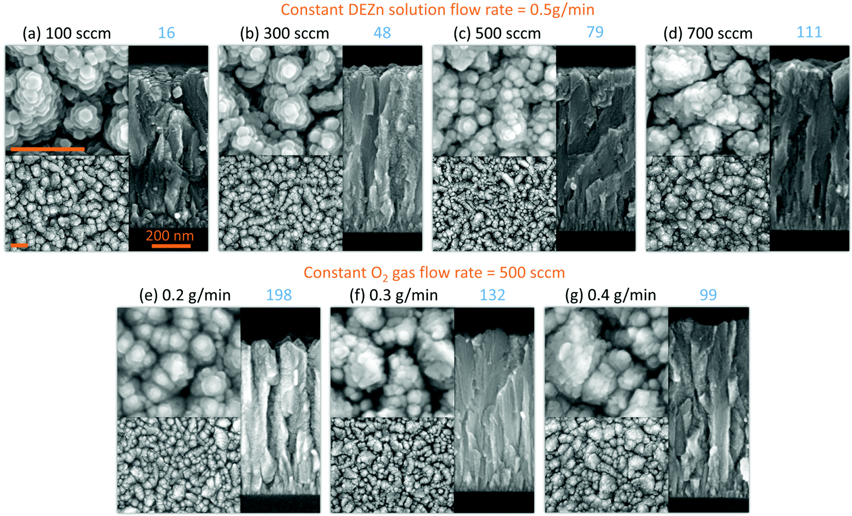 | ||
| Fig. 1 Top-view (left) and cross-sectional-view (right) FESEM images of ZnO thin films grown by PLI-MOCVD with the (a) 100, (b) 300, (c) 500, and (d) 700 sccm O2 gas flow rate for a given DEZn solution flow rate of 0.5 g min−1; or with the (e) 0.2, (f) 0.3, and (g) 0.4 g min−1 DEZn solution flow rate for a given O2 gas flow rate of 500 sccm. The corresponding O2/DEZn molar flow rate ratios are indicated in blue. The scale bars correspond to 200 nm. | ||
The mean growth rate deduced from the ratio of the thickness of ZnO thin films over their growth time and its dependence on the O2 gas and DEZn solution flow rates as well as on the corresponding O2/DEZn ratio are presented in Fig. 2. The mean growth rate of ZnO thin films continuously increases as the DEZn solution flow rate is increased for a given O2 gas flow rate of 500 sccm, as shown in Fig. 2a. The faster growth of ZnO thin films at higher DEZn solution flow rate indicates that the growth rate is here limited by the amount of available Zn reactant; in other words, the Zn reactant acts as the limiting species in the PLI-MOCVD growth process. In contrast, the mean growth rate of ZnO thin films continuously decreases as the O2 gas flow rate is increased for a given DEZn solution flow rate of 0.5 g min−1, as revealed in Fig. 2b. It should be noted that, when the O2 gas flow rate is increased, the mixed Ar flow rate was decreased with the same amount in order to maintain the same gas volume introduced into the reactor chamber for all PLI-MOCVD growth conditions. As the reactor chamber pressure was kept constant at 3 mbar, the Zn reactant flux introduced was not be pushed out by the increasing O2 gas flow rate. The higher O2 gas flow rate actually increases the probability of reaction between the O and Zn reactants in their gas phase, which reduces the amount of available Zn reactant reaching the substrate and leads to the decrease in the mean growth rate of ZnO thin films. In Fig. 2c, the mean growth rate is found to monotonically decrease as the O2/DEZn flow rate ratio is increased, indicating again that the amount of available Zn reactant limits the PLI-MOCVD growth process in both series despite the two different manners of changing the flow rate conditions.
 | ||
| Fig. 2 Evolution of the mean growth rate of ZnO thin films grown by PLI-MOCVD as a function of (a) the DEZn solution flow rate for a given O2 gas flow rate of 500 sccm, (b) the O2 gas flow rate for a given DEZn solution flow rate of 0.5 g min−1 and (c) the O2/DEZn flow rate ratio. | ||
The Raman scattering spectra of ZnO thin films grown by PLI-MOCVD with various O2 gas and DEZn solution flow rates are presented in Fig. 3a. Only two Raman lines characteristic of the ZnO wurtzite structure are visible in the spectra. They are located at 99 and 438 cm−1 and assigned to the Elow2 and Ehigh2 modes, respectively.35,36 In addition, two large broad bands attributed to C–C bonds occur at around 1360 and 1580 cm−1 regardless of the flow rate conditions, indicating the carbon contamination in ZnO thin films due to the use of organic compounds in the PLI-MOCVD growth process.37 The carbon contamination can be suppressed following a thermal annealing under oxygen atmosphere at high temperature, as previously reported in ref. 30. The Raman lines labelled with an asterisk in the spectra are related to the silicon substrate. Both the Elow2 and Ehigh2 mode-related Raman lines exhibit a higher intensity when the ZnO thin films are grown with the 100 sccm O2 gas and 0.2 g min−1 DEZn solution flow rates, revealing that the crystallinity is better in these two thin films. Interestingly, it is worth noticing that the thin film grown with the O2 gas flow rate of 100 sccm has the highest mean growth rate, while the thin film grown with the DEZn solution flow rate of 0.2 g min−1 has the lowest mean growth rate, as shown in Fig. 2. This indicates that the ZnO thin films with a high crystallinity can be deposited within a broad range of growth rates.
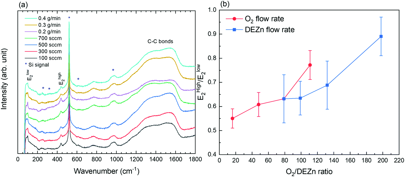 | ||
| Fig. 3 (a) Raman scattering spectra of ZnO thin films grown by PLI-MOCVD with various O2 gas and DEZn solution flow rates. The intensity was plotted in logarithmic scale. (b) Evolution of the Ehigh2/Elow2 intensity ratio as a function of the O2/DEZn flow rate ratio. | ||
The evolution of the Ehigh2/Elow2 intensity ratio in the ZnO thin films grown by PLI-MOCVD and its dependence on the O2/DEZn flow rate ratio are presented in Fig. 3b. The intensities of the Ehigh2 and Elow2 mode-related Raman lines in ZnO thin films were extracted within a fitting procedure using a Lorentzian function in Origin 2018b software, as shown in Fig. S2 (ESI†). Since the Ehigh2 mode is mainly related to the O atom lattice vibration while the Elow2 mode is mostly related to the Zn atom lattice vibration in the wurtzite structure,35,36 their intensity ratio gives an insight into the chemical composition of ZnO thin films through the O/Zn atomic ratio. The variation of the Ehigh2/Elow2 intensity ratio reveals that the chemical composition of ZnO thin films is influenced by the change of the O2 gas and DEZn solution flow rates. In particular, the Ehigh2/Elow2 intensity ratio is found to significantly increase as the O2/DEZn flow rate ratio is increased from 16 to 198. This shows that the ZnO thin films exhibit a larger O/Zn atomic ratio when the O2/DEZn flow rate ratio is increased, namely a larger amount of O atoms with respect to Zn atoms. As the O2/DEZn flow rate ratio is increased, the more oxidizing conditions are associated with an increased oxygen chemical potential during the PLI-MOCVD growth process. This gives rise to the formation of a larger concentration of Zn vacancies with a low formation energy when the Femi level is close to the conduction band minimum, as reported by density-functional theory calculations in ref. 31. These Zn vacancies, formed with a larger concentration for a higher O2/Zn flow rate ratio, act as deep acceptors in the ZnO thin films.
The XRD patterns of ZnO thin films grown by PLI-MOCVD with various O2 gas and DEZn solution flow rates are presented in Fig. 4. The diffraction peaks located at 31.8, 34.4, 36.3, 47.5, 62.9, 72.6, and 125.1° are attributed to the 100, 002, 101, 102, 103, 004, and 006 reflections of the ZnO wurtzite structure, respectively, as indicated by the corresponding ICDD file labelled 00-036-1451. The intensity, position, and FWHM of diffraction peaks were extracted within a fitting procedure using a Pseudo-Voigt function in Origin 2018b software, as shown in Fig. S3 (ESI†). Despite the difference in their morphology, the XRD patterns of all the ZnO thin films are overall fairly similar. The intensity of the 002 diffraction peak is systematically much larger than the intensity of the other diffraction peaks, indicating that the growth direction is strongly aligned along the polar c-axis, as shown in Fig. 4a. The growth texture of ZnO thin films follows the evolutionary selection model given by van der Drift, in which the grains with the fastest growth direction predominantly develop and dominate the overall orientation.38 In the present case, the polar c-planes are well-known to exhibit the higher surface energy in the wurtzite structure and thus the larger surface reactivity enhancing their development,39 in turn governing the growth texture of ZnO thin films. In comparison, the ZnO thin films grown by MOCVD in ref. 20 underwent a morphology transition accompanied by the change of the growth direction from the polar c-axis to the non-polar a-axis and vice versa when the H2O and DEZn flow rates were varied. The zoom-in in the area of interest of the XRD patterns in Fig. 4b however shows that the position and FWHM of the main diffraction peaks depend on the O2 gas and DEZn solution flow rates. The intensity, position, and FWHM of the diffraction peaks were exploited to investigate the evolution of the orientation, homogeneous strain, inhomogeneous strain caused by microstructural defects, and crystallite size of ZnO thin films as a function of the O2 gas and DEZn solution flow rates as presented in Fig. 5–7.
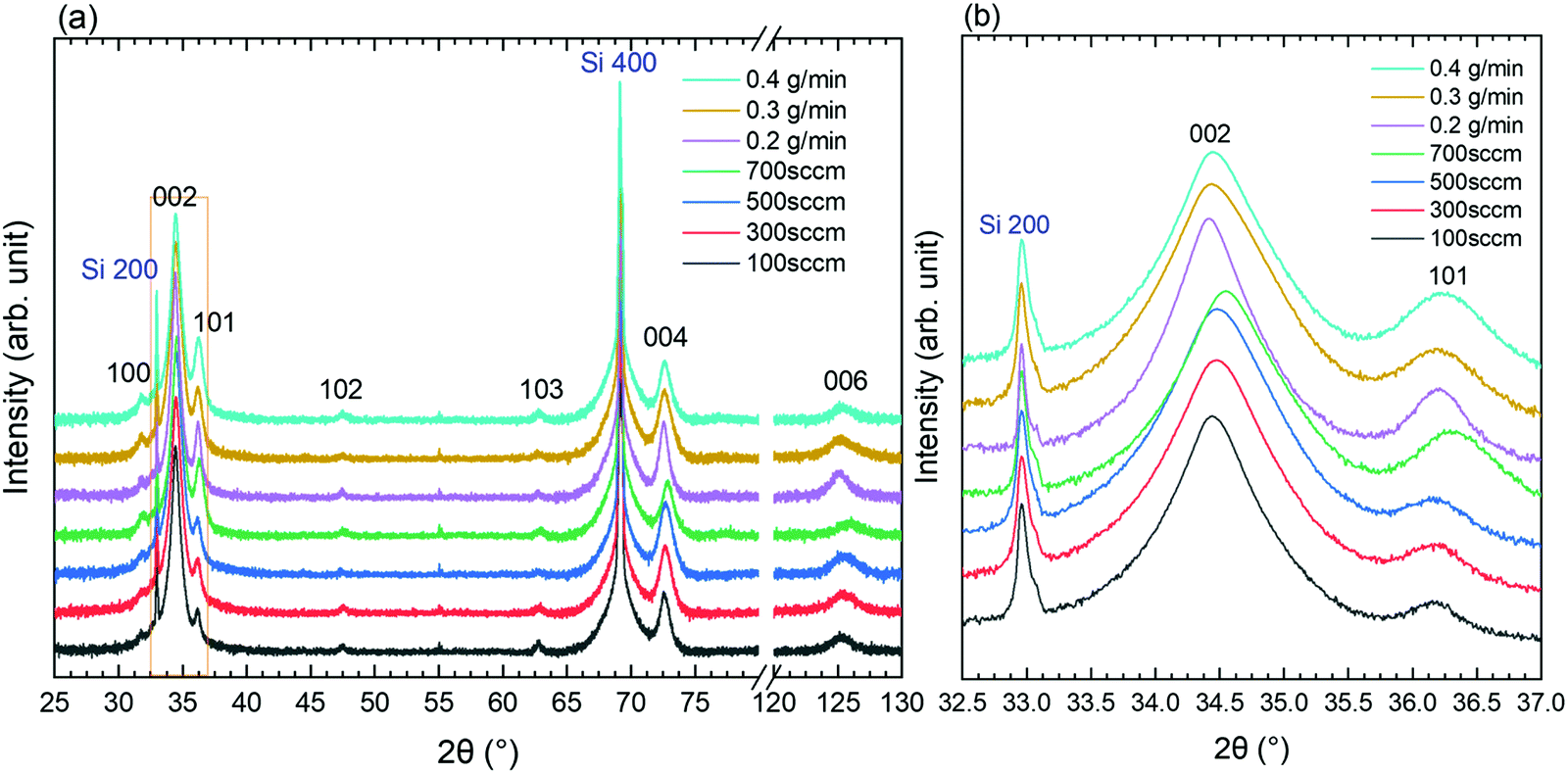 | ||
| Fig. 4 (a) XRD of ZnO thin films grown by PLI-MOCVD with various O2 gas and DEZn solution flow rates; (b) Zoom-in in the area of interest ranging from 32.5 to 37° in the XRD patterns. The intensity was plotted in logarithmic scale. | ||
 | ||
| Fig. 5 Evolution of the 002 texture coefficient as a function of the (a) O2 gas flow rate, (b) DEZn solution flow rate, and (c) O2/DEZn flow rate ratio. Evolution of the 100, 101, 102 and 103 texture coefficients as a function of the (d) O2 gas flow rate, (e) DEZn solution flow rate, and (f) O2/DEZn flow rate ratio. | ||
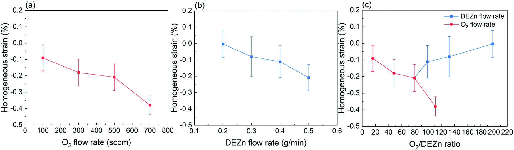 | ||
| Fig. 6 Evolution of the mean homogenous strain as a function of the (a) O2 gas flow rate, (b) DEZn solution flow rate, and (c) O2/DEZn flow rate ratio. | ||
 | ||
| Fig. 7 Evolution of the mean inhomogeneous strain as a function of the (a) O2 gas flow rate, (b) DEZn solution flow rate, and (c) O2/DEZn flow rate ratio. Evolution of the average crystallite size as a function of the (d) O2 gas flow rate, (e) DEZn solution flow rate, and (f) O2/DEZn flow rate ratio. | ||
As the O2 gas flow rate is increased from 100 to 500 sccm, the 002 texture coefficient of ZnO thin films slightly increases from 99.5 to 99.7%, indicating a small improvement of the orientation along the polar c-axis (Fig. 5a). This enhancement is correlated with the change of the grain morphology from the flat hexagonal shape to the smaller and sharper shape, as shown in Fig. 1a–c. The more significant decrease in the 002 texture coefficient of ZnO thin films grown with the O2 gas flow rate of 700 sccm to 98.8% can be related to the sudden formation of large-sized clusters, as seen in Fig. 1d. Simultaneously, the other texture coefficients increase in this thin film, especially in the direction normal to the (101) plane (Fig. 5d). This result shows that the growth rate along the polar c-axis relatively decreases compared to other growth directions in that condition. As the DEZn solution flow rate is decreased from 0.5 to 0.4 g min−1, the 002 texture coefficient also decreases to 98.6% as seen in Fig. 5b, while the texture coefficients of the other planes increase as indicated in Fig. 5e. It is noticeable that the thin film grown with a DEZn solution flow rate of 0.4 g min−1 and the other one grown with a O2 gas flow rate of 700 sccm exhibit a similar behaviour concerning the grain morphology and texture coefficient. As the DEZn flow rate continues to decrease from 0.4 to 0.2 g min−1, the 002 texture coefficient gradually increases again to 99.4% as seen in Fig. 5b, while the texture coefficients of the other planes decrease as indicated in Fig. 5e. This is concomitant with the decrease in the density of large-sized clusters as observed in the thin film grown with the DEZn solution flow rate of 0.2 and 0.3 g min−1, as seen in Fig. 1e and f. As compared to the other thin films which contain no large-sized cluster in their morphology, the 002 texture coefficient of the thin film grown with the DEZn solution flow rate of 0.2 g min−1 exhibiting the lowest density of large-sized cluster is still lower. These results show that the flat hexagonal or round grains in the thin films exhibit a preferential orientation along the polar c-axis in contrast to the large-sized clusters. Nevertheless, the texture coefficients of all ZnO thin films are larger than 98%, presenting the highly c-axis oriented structure regardless of the flow rate conditions. This is opposite to the result reported in ref. 20, in which the preferential orientation of the ZnO thin film was switched from the non-polar a-axis to the polar c-axis by varying the DEZn and H2O vapour flow rates. The discrepancy is possibly due to the different MOCVD system used and to the significantly distinct growth conditions through the use of H2O vapour instead of O2 molecules as well as other growth temperature and pressure as compared to our growth conditions.
The mean homogeneous strain of ZnO thin films as presented in Fig. 6 shows a negative value regardless of the flow rate conditions. This indicates that the residual strain along the polar c-axis in all ZnO thin films is compressive. In other words, the biaxial stress (i.e. in the plane) of all ZnO thin films is tensile and originates from the Volmer–Weber growth mode. The growth of polycrystalline ZnO thin films initiates through the formation of isolated islands further undergoing a coalescence process, during which a significant tensile biaxial stress is generated and can partially or entirely be relieved by the excess incorporated atoms at grain boundaries during the film thickening.40–42 Here, the total strain relaxation is not entirely reached, except in the thin film grown with the DEZn solution flow rate of 0.2 g min−1 exhibiting a better crystallinity as revealed from Raman scattering spectra. It is also efficient in the thin film grown with the 100 sccm O2 gas flow rate for the same reason. Fig. 6a and b reveal that the magnitude of the mean homogeneous strain increases when either the O2 gas or DEZn solution flow rates are increased. In the case of the evolution of the mean homogeneous strain with the O2 gas flow rate, the variation of the grain morphology should be taken into account. Apparently, the mean homogeneous strain is smaller in the thin film grown with the O2 gas flow rate of 100 sccm, where large grain size and grain gap are revealed in Fig. 1a. In contrast, it is larger in the thin films grown with the O2 gas flow rate of 300 and 500 sccm, where smaller grain size and grain gap are shown in Fig. 1b–c. On the basis of the origin of the tensile biaxial stress generated during the Volmer–Weber growth mode, the morphology with less compact and bigger grains as seen in the thin film grown with the O2 gas flow rate of 100 sccm should present the smallest tensile biaxial stress and thus the smallest residual strain. When small grains grow and coalesce to form bigger grains, the surface free energy at grain boundaries can also be removed such that more intrinsic stress inside the film is relieved.40 The mean homogeneous strain is the largest one in the thin film grown with the O2 gas flow rate of 700 sccm, where compact large-sized clusters of small grains are formed as seen in Fig. 1d. However, the results also show that the mean homogeneous strain is pretty low in the film grown with the 0.4 g min−1 DEZn exhibiting compact large-sized clusters of small grains as seen in Fig. 1g. Despite the similar morphologies, the mean homogeneous strain in the thin film grown with the 0.5 g min−1 DEZn solution and 700 sccm O2 gas flow rates and in the thin film grown with the 0.4 g min−1 DEZn solution and 500 sccm O2 gas flow rates is significantly different. This suggests that the mean homogeneous strain is more dependent upon the flow rates than upon the morphology or the O2/DEZn flow rate ratio, as presented in Fig. 6c. Both the flow rate related to the atom density and the morphology related to the surface roughness can affect the surface energy and the diffusion of atoms at the grain boundaries, which are the causes of the homogeneous residual strain in thin films during its thickening stage.42 The increase in the mean homogenous strain of ZnO thin films as the O2 gas and DEZn solution flow rates are increased could be due to the fact that the high flow rate environment prevents the surface diffusion of atoms out of or into the grain boundaries favouring the relaxation. For instance, the thin films grown with the 700 sccm O2 gas flow rate and with the 0.5 g min−1 DEZn solution flow rate exhibit the highest flow rates in both series and correlatively the largest shift of the 002 diffraction peak (Fig. 4b) corresponding to its largest compressive homogeneous strain (Fig. 6a and b).
The mean inhomogeneous strain and average crystallite size calculated by using the Williamson-Hall plot are presented in Fig. 7 as a function of the O2 gas and DEZn solution flow rates. The Williamson–Hall plots of ZnO thin films are reported in Fig. S4 (ESI†). The mean inhomogeneous strain in Fig. 7a and b increases as the O2 gas and DEZn solution flow rates are increased. It has its lowest magnitudes in the thin films grown with the 100 sccm O2 gas and 0.2 g min−1 DEZn solution flow rates exhibiting a better crystallinity as revealed from Raman scattering spectra. In the case of its evolution with the O2 gas flow rate, it increases when increasing the flow rate from 100 to 500 sccm, and then decreases at 700 sccm. In the case of its evolution with the DEZn solution flow rate, it also increases when increasing the flow rate from 0.2 to 0.3 g min−1, then decreases slightly at 0.4 g min−1, and eventually increases again at 0.5 g min−1. It turns out that the increase in the mean inhomogeneous strain with the O2 gas and DEZn solution flow rates as seen in Fig. 7c is disrupted for the two thin films exhibiting a similar high number density of large-sized clusters as presented in Fig. 1d and g. Notably, the mean inhomogeneous strains in the thin film grown with the 700 sccm O2 gas and 0.5 g min−1 DEZn solution flow rates and in the thin film grown with the 500 sccm O2 gas and 0.4 g min−1 DEZn solution flow rates are very similar and equal to 0.44 and 0.43%, respectively. This shows that the mean inhomogeneous strain is more dependent upon the morphology than upon the flow rates for some of the MOCVD conditions, which differs from the mean homogeneous strain. Since the mean inhomogeneous strain is caused by microstructural defects in the ZnO thin films, the type and density of incorporated defects depend on the O2 gas and DEZn solution flow rates. Among the thin films with the similar morphology, the mean inhomogeneous strain is usually smaller as the O2 gas flow rate or DEZn solution flow rate are lower. This could be due to the fact that the higher surface diffusion of atoms in the lower flow rate environment enhances the atom arrangement during the growth leading to the formation of thin films with a better crystallinity.20
Fig. 7d–f shows that the average crystallite size of thin films lies in the range of 20–50 nm, which is similar to ref. 22. It should be noted that since the XRD pattern was scanned within an out-of-plane configuration, the calculated average crystallite size represent the vertical dimension of domains that is normal to the substrate. It is shown that the thin film grown with the 500 sccm O2 gas and 0.5 g min−1 DEZn solution flow rates has the highest average crystallite size at around 52 nm. This is related to its higher mean growth rate along the polar c-axis, which is supported by its highest 002 texture coefficient. Conversely, the thin films grown with the 700 sccm O2 gas and 0.4 g min−1 DEZn solution flow rates have the smallest average crystallite size at around 24.5 and 21.5 nm owing to their lower mean growth rate along the polar c-axis, which is also suggested by their lower 002 texture coefficients. The average crystallite size of ZnO thin films is thus strongly dependent upon their mean growth rate along the polar c-axis.
Overall, the XRD analysis demonstrates that the orientation as well as the mean homogeneous and inhomogeneous strain along with the average crystallite size are affected by the O2 gas and DEZn solution flow rates and by the resulting O2/DEZn flow rate ratio. While the variation of the mean homogeneous strain is more related to the flow rates rather than the O2/DEZn flow rate ratio, the orientation and inhomogeneous strain together with the morphology seem to have a stronger relation with the O2/DEZn flow rate ratio. In particular, the sudden morphology change from flat hexagonal/round grains to large-sized clusters (Fig. 1), the disrupted variation in the orientation (Fig. 5c) and mean inhomogeneous strain (Fig. 7c) occur when the O2 gas flow rate increases from 500 to 700 sccm, or when the DEZn solution flow rate decreases from 0.5 to 0.4 g min−1, corresponding to the O2/DEZn flow rate ratio lying in the narrow range of 99-111.
3.2 Effects of the flow rates on the crystal polarity, piezoelectric response, and resistivity
The PFM results collected on the ZnO thin films reporting their topography together with their piezoelectric amplitude and phase are presented in Fig. 8. The root mean square (RMS) roughness was deduced from the topography of the ZnO thin films by using NanoScope Analysis v200r1 software. The RMS roughness of the ZnO thin film grown with the 0.5 g min−1 DEZn solution and 100 sccm O2 gas flow rates is of about 21 nm, reflecting its large grain size and grain gap. When the O2 gas flow rate is increased to 500 sccm, the RMS roughness of the ZnO thin film gradually decreases to about 8 nm, corresponding to its smaller grain size and grain gap. The RMS roughness is around 21 nm for the ZnO thin film grown with the 700 sccm O2 gas flow rate and for other ZnO thin films grown with the 500 sccm O2 gas flow rate but with a lower DEZn solution flow rate owing to the occurrence of large-sized clusters. By removing interferences due to electrostatic effects using the high stiffness tip during PFM scanning, the piezoelectric amplitude is proportional to the piezoelectric coefficient and applied voltage amplitude.43,44 The brighter domains in the piezoelectric amplitude images indicate the domains with the higher piezoelectric coefficients, and vice versa. The piezoelectric phase with respect to the applied voltage phase identifies the domain polarity. Within our PFM set-up, the domains with the piezoelectric phase at around 70° (bright area) represent the Zn-polarity domains, while the domains with the piezoelectric phase at around −90° (dark area) represent the O-polarity domains.29 The relation between the piezoelectric phase and crystal polarity of the domains was confirmed by performing PFM measurements on ZnO single crystals with an identified O- or Zn-polarity.29 The piezoelectric phase images reveal a significant variation of the polarity of domains among the thin films grown with various O2 gas and DEZn solution flow rates. The large change of the polarity distribution is attributed to the sudden morphology change from round-shaped grains to highly dense large-sized clusters when the O2 gas flow rate is increased from 500 to 700 sccm and when the DEZn flow rate is decreased from 0.5 to 0.4 g min−1. By comparing the topography with the piezoelectric phase images, it is shown that the hexagonal- and round-shaped grains in the thin films grown with the 100, 300, and 500 sccm O2 gas flow rates exhibit the Zn-polar signals (Fig. 8a–i), while the large-sized clusters in the thin film grown with the 700 sccm O2 gas flow rate have the O-polar signals along with the Zn-polar signals from surrounding smaller grains (Fig. 8j–l and v–x). In the thin film grown with the 500 sccm O2 gas flow rate, some domains with the mix of dark and bright piezoelectric phases occur (Fig. 8i), which can be due to the neutralization of two domains with an opposite polarity that are stacked together. In the thin films grown with the 0.2, 0.3, and 0.4 g min−1 DEZn solution flow rates, it is also revealed that the O-polar signals originates from the large-sized clusters while the Zn-polar signals comes from the smaller round-shaped grains (Fig. 8m–u). The difference in the grain sizes and shapes exhibiting the two opposite polarities shows their distinct growth mechanism. The reason for this polarity change with the O2 gas and DEZn solution flow rates could be due to their influence on the surface energy of crystalline planes, which in turn affects the growth direction. The surface energies of the Zn- and O-polar c-planes were computed by DFT calculations in ref. 45, in which it was shown that the O-polar c-plane is more stable than the Zn-polar one in the O-rich conditions, namely as the O2/DEZn grow rate ratio is increased. While the growth direction along the polar c-axis is governed by the evolutionary selection given by the van der Drift model,38 the minimization of the surface energy of the polar c-plane acts as a driving force to develop the O-polarity domains and thus to select the polarity in the thin films as the thickening stage proceeds. This accounts for the formation and preferential development of O-polarity domains in the thin films grown with the higher O2/DEZn flow rate ratios, as seen in Fig. 8l, o, r and u.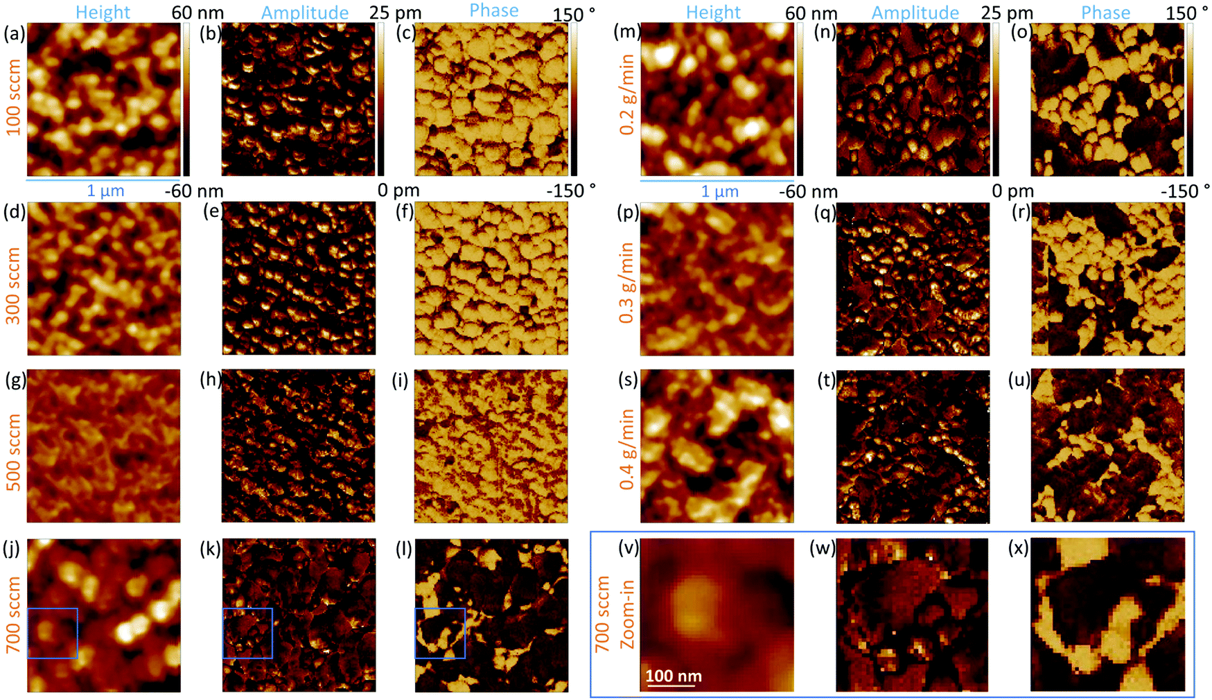 | ||
| Fig. 8 Topography, piezoelectric amplitude, and piezoelectric phase of ZnO thin films grown by PLI-MOCVD with the (a–c) 100, (d–f) 300, (g–i) 500, and (j–l) 700 sccm O2 gas flow rate for a given DEZn solution flow rate of 0.5 g min−1; or with the (m–o) 0.2, (p–r) 0.3, (s–u) 0.4 g min−1 DEZn solution flow rate for a given O2 gas flow rate of 500 sccm. (v–x) Zoom-in in the area of interest in the thin film grown with the O2 gas flow rate of 700 sccm. | ||
The PFM results are further investigated by analysing the piezoelectric amplitude and phase histograms, which were obtained from their amplitude and phase images by using NanoScope Analysis v200r1 software. To separate the piezoelectric amplitudes of the Zn-polarity, O-polarity, and non-polar domains, the data points from the PFM images were treated as follows: the data points with the piezoelectric phase higher than 50° had their piezoelectric amplitude unchanged and were assigned to the Zn-polarity domains, while the data points with the piezoelectric phase lower than −50° had their piezoelectric amplitude multiplied by −1 and were assigned to the O-polarity domains. Other data points were assigned to non-polar domains and were removed. The piezoelectric amplitude histogram of data points after treatment is shown in Fig. 9. The raw histograms of the piezoelectric amplitude and phase are reported in Fig. S5 (ESI†). The histograms of thin films grown with the 100, 300 and 500 sccm O2 gas flow rate show that most of the piezoelectric domains are Zn-polar, reflecting the piezoelectric signals from the hexagonal- and round- shaped grains (Fig. 9a–c). The piezoelectric amplitudes of the domains with a mix of the positive and negative piezoelectric phases in the thin films grown with the 500 sccm O2 gas flow rate were removed from the histogram in Fig. 9c following the data treatment. Conversely, almost all the piezoelectric domains in the thin film grown with the 700 sccm O2 gas flow rate are O-polar (Fig. 9d), reflecting the piezoelectric signals from the large-sized clusters. Among the thin films grown with the lower DEZn flow rate, the thin film grown at 0.4 g min−1 also shows that most of the piezoelectric domains are O-polar owing to the high number density of large-sized clusters (Fig. 9g). The thin films grown with the 0.2 and 0.3 g min−1 DEZn solution flow rates have a mix of domains with the O- and Zn-polarity, corresponding to the coexistence of Zn-polar small round-shaped grains and O-polar large-sized clusters on these thin films (Fig. 9e and f). The histograms also show that the piezoelectric amplitude distribution on the Zn-polarity domains stretches to a higher value as compared to the one on the O-polarity domains. This is illustrated by the brighter spots in the piezoelectric amplitude images, which corresponds to an amplitude that is higher than 20 pm. These bright spots only occur on the Zn-polarity domains, while the less bright O-polarity domains show a lower piezoelectric amplitude. This indicates that the piezoelectric efficiency is larger on the Zn-polarity domains than on the O-polarity domains. The reason could be due to the higher concentration of impurities incorporated into O-polar domains than into Zn-polar domains of ZnO thin film grown by MOCVD. It was shown in ref. 13 that there is much more impurity incorporation in ZnO films grown on O-polar ZnO substrate by chemical vapour deposition as compared to on the Zn-polar ZnO substrate. The larger amount of those impurities acting as shallow donors and incorporated in the O-polarity domains increases the screening effect that decreases the resulting piezoelectric efficiency as compared to the Zn-polarity domains.1–4
 | ||
| Fig. 9 Piezoelectric amplitude histogram after data treatment of ZnO thin films grown by PLI-MOCVD with the (a) 100, (b) 300, (c) 500, (d) 700 sccm O2 gas flow rate for a given DEZn solution flow rate of 0.5 g min−1; or with the (e) 0.2, (f) 0.3, (g) 0.4 g min−1 DEZn solution flow rate for a given O2 gas flow rate of 500 sccm. | ||
The mean piezoelectric amplitude on the Zn- and O-polarity domains along with the Zn-polarity domain percentage were calculated on the basis of the data after treatment. The Zn-polarity domain percentage was inferred from the ratio of the Zn-polarity domain data point amount to the total amount of Zn- and O-polarity domain data points excluding the non-polar domain data points. It is revealed in Fig. 10a–c that the piezoelectric amplitude of Zn-polarity domains are fairly similar at around 10 pm among the thin films, except the thin film grown with the 700 sccm O2 gas flow rate where it decreases to 8.7 pm. On the other hand, the piezoelectric amplitude of O-polarity domains increases from 5.2 to 7.7 pm when the O2 flow rate is increased from 100 to 700 sccm. The piezoelectric amplitude of O-polarity domains further increases from 6.6 to 8.4 when the DEZn flow rate is decreased from 0.5 to 0.2 g min−1. Importantly, Fig. 10c also shows that the piezoelectric amplitude of O-polarity domains continuously increases with the O2/DEZn flow rate ratio. This is certainly due to the less incorporation of residual impurities acting as shallow donors such as AlZn and GaZn at higher oxygen chemical potential when the O2/DEZn flow rate ratio increases,46 leading to the reduction of the screening effect.1–4 In Fig. 10d–f, the high Zn-polarity domain percentage at around 85% in the thin films grown with the 100, 300, and 500 sccm O2 gas flow rate indicates the predominant Zn-polarity. The high Zn-polarity domain percentage drastically decreases to 14.5 and 25% as the O2 gas flow rate is increased from 500 to 700 sccm and as the DEZn solution flow rate is decreased from 0.5 to 0.4 g min−1, indicating the predominant O-polarity in these films. The medium value of the Zn-polarity domain percentages at around 40-50% in the thin films grown with the 0.2 and 0.3 g min−1 DEZn solution flow rate reveals the coexistence of both polarities. The very low Zn-polarity domain percentage corresponding to the predominant O-polarity in the thin film grown with the 700 sccm O2 gas flow rate shows that the Zn-polarity domains could be so small that the measured amplitudes on these Zn-polar grains can be interfered and reduced by the 180°-out-of-phase amplitude of the O-polar grains underneath them, leading to the lower Zn-polar piezoelectric amplitude on this film compared to other thin films as shown in Fig. 10a–c. In comparison, the lowest O-polar piezoelectric amplitude of thin films grown with the 100 and 300 sccm O2 gas flow rate could be due to the fact that the measured piezoelectric amplitudes of O-polar grains are neutralized by the piezoelectric amplitudes of Zn-polar grains underneath them, which is suggested by the predominant Zn-polarity on these thin films. The similar Zn-polar piezoelectric amplitude and high O-polar piezoelectric amplitude in the thin films grown with the 0.2 and 0.3 g min−1 DEZn solution flow rate as compared to other thin films show that both polarity coexists on these thin films with large enough grain size without amplitude neutralization.
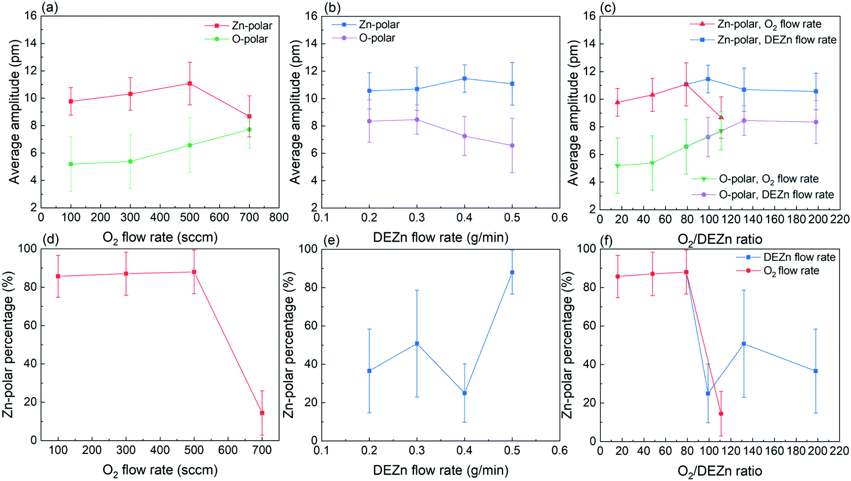 | ||
| Fig. 10 Evolution of the mean piezoelectric amplitude on the Zn- and O-polarity domains as a function of the (a) O2 gas flow rate, (b) DEZn solution flow rate, and (c) O2/DEZn flow rate ratio. Evolution of the Zn-polarity domain percentage as a function of the (d) O2 gas flow rate, (e) DEZn solution flow rate, and (f) O2/DEZn flow rate ratio. | ||
The resistivity of ZnO thin films was also measured by the TLM method. The detailed TLM results are presented in Fig. 11a along with the evolution of the resistivity as a function of the O2 gas and DEZn solution flow rates. Overall, the resistivity of ZnO thin films is varied in the range of 0.5–11.7 Ω cm as seen in Fig. 11b. Its value increases from 2.7 to 11.7 Ω cm as the O2 gas flow rate is increased from 100 to 500 sccm and then falls down to 0.5 Ω cm for a O2 gas flow rate of 700 sccm (Fig. 11c). In contrast, its value slightly decreases from 3.9 to 2.2 Ω cm as the DEZn solution flow rate is increased from 0.2 to 0.4 g min−1 and then jumps up to 11.7 Ω cm for a DEZn solution flow rate of 0.5 g min−1 (Fig. 11d). Interestingly, the thin films with the resistivity higher than 10 Ω cm systematically exhibit highly predominant Zn-polarity domains. Correlatively, the thin films with the resistivity lower than 1 Ω cm exhibit highly predominant O-polarity domains. This supports the fact that Zn-polarity domains likely have a smaller concentration of residual impurities in their centre in contrast to O-polarity domains and hence exhibit a higher piezoelectric amplitude.
 | ||
| Fig. 11 (a) Evolution of the total resistance of ZnO thin films grown by PLI-MOCVD as a function of the distance between electrode pairs using the TLM method. (b) Evolution of the resistivity of ZnO thin films as a function of the (b) O2/DEZn flow rate ratio, (c) O2 gas flow rate, and (d) DEZn solution flow rate. | ||
These PFM and TLM results demonstrate the strong correlation of the piezoelectric properties of ZnO thin films grown by PLI-MOCVD with their morphological, structural, and electrical properties. First, the crystal polarity of ZnO thin films changes while their morphology undergoes a significant transition when the O2 gas and DEZn solution flow rates are varied. The Raman spectrum analysis reveals that the increase in the O2/DEZn flow rate ratio leads to the increase in the O/Zn atomic ratio in ZnO thin films by inducing more oxidizing conditions corresponding to the higher oxygen chemical potential. This can affect the surface energy of ZnO crystalline planes that results in altering the growth direction as well as the crystal polarity. A different grain shape between the predominantly O- and Zn-polar ZnO thin films is shown in the topography and piezoelectric phase maps (Fig. 8), implying their different growth mechanisms. Second, the remarkable switch of the crystal polarity of ZnO thin films from predominant Zn-polarity to predominant O-polarity is correlated with the disrupted changes of the texture coefficient (Fig. 5c) and of the inhomogeneous strain (Fig. 7c) as observed in the XRD results when the O2/DEZn flow rate ratio lies in the narrow range of 99–111. It is revealed that the increase in the density of O-polar large-sized clusters is strongly correlated with the decrease in the 002 texture coefficient. This indicates that the ZnO thin films with the O-polar large-sized clusters have a lower c-axis crystal orientation as compared to the one with the Zn-polar hexagonal/round grains. The disrupted change of the inhomogeneous strain is further associated with the large change of Zn-polarity domain percentage when the O2/DEZn flow rate ratio ranges from 99 to 111. This suggests the different nature and density of microstructural defects between the O- and Zn-polarity domains. The difference of the incorporation of residual impurities between both O- and Zn- polarity domains as suggested by TLM results,46 which could cause screening effect by free charge carriers, can lead to different piezoelectric efficiency.47,48 This is typically observed in the PFM measurements, showing that the piezoelectric amplitude is lower on the O-polarity domains than on the Zn-polarity domains.
4. Discussion
In summary, the evolution of the morphological, structural, and piezoelectric properties of ZnO thin films grown by PLI-MOCVD with the DEZn solution and O2 gas flow rates as well as with the O2/DEZn flow rate ratio is illustrated in Fig. 12. Regardless of the DEZn solution and O2 gas flow rates, the growth rate of ZnO thin films is limited by the amount of available Zn reactants. The growth texture and tuneable crystal polarity of ZnO thin films are explained by the evolutionary selection model given by van der Drift that is further revisited to take into account the variation of oxygen chemical potential through the variation of the O2/DEZn flow rate ratio.38 In that model, the grains with the fastest growth direction predominantly develop and dominate the overall orientation. At low O2 gas flow rate or low O2/DEZn flow rate ratio ranging from 16 to 99, the growth of ZnO thin films is highly oriented along the polar c-axis, but the growth rate on the more reactive c+-plane with the Zn-polarity is larger due to its higher surface energy as compared to the c−-plane with the O-polarity in more reducing conditions (i.e. with a lower oxygen chemical potential).45 This results in the predominance of Zn-polarity domains with a flat, hexagonal shape in ZnO thin films grown in this range. When the O2 gas flow rate is increased and correlatively the O2/DEZn flow rate ratio lies in the range of 99–111, the growth rate gets larger on the c−-plane with the O-polarity than on the c+-plane with the Zn-polarity owing to its higher surface energy in more oxidizing conditions (i.e. with a higher oxygen chemical potential).45 Thus, the ZnO thin films grown in this range exhibit the occurrence of predominant O-polarity domains in the form of large-sized clusters. When the DEZn solution flow rate is decreased and hence at higher O2/DEZn flow rate ratio ranging from 111 to 198, the growth rate in both polar directions is fairly similar, leading to the coexistence of O- and Zn-polarity domains. In those extremely O-rich conditions, the development of polar domains is also highly dependent upon the ability of the available Zn reactant as the very limiting species to incorporate on the growing front.49 Since the Zn-polarity domains present three dangling bonds per O atom on their surface while the O-polarity domains exhibit one dangling bond per O atom on their surface, the incorporation rate of Zn atoms is much larger in the Zn-polarity domains.50 This explains why the Zn-polarity domains coexist with the O-polarity domains that are further more reactive. The flow rate conditions also have a major influence on the incorporation of residual impurities in the bulk of ZnO thin films, which can in turn affect the piezoelectric amplitude. The more oxidizing conditions corresponding to the increase in the O2/DEZn flow rate ratio are favourable for increasing the concentration of zinc vacancies.31 They further reduce the incorporation of shallow donors such as AlZn and GaZn, which present a higher formation energy on the O-polarity domains,46 leading to the increase in their piezoelectric amplitude by reducing the screening effect.47,48 However, this phenomenon has less effect on the piezoelectric amplitude of Zn-polarity domains because the incorporation of shallow donors is less pronounced here.13 Overall, the piezoelectric amplitude is systematically higher on the Zn-polarity domains than on the O-polarity domains, indicating that the uniform Zn-polar ZnO structure can lead to a high piezoelectric efficiency. Further improvement of ZnO piezoelectric efficiency can be achieved by introducing dopants to reduce the screening effect.3 The optimization of the electrodes and the design for the piezoelectric device can also be carried out to maximize the ZnO piezoelectric performance.51 | ||
| Fig. 12 Schematic representing the dependence of the morphological, structural, and piezoelectric properties of ZnO thin films grown by PLI-MOCVD on the DEZn solution and O2 gas flow rate conditions. | ||
5. Conclusions
By sequentially varying the O2 gas and DEZn solution flow rates during the PLI-MOCVD growth process of ZnO thin films, their morphological, structural, electrical, and piezoelectric properties have been found to be affected by the resulting O2/DEZn flow rate ratio. A comprehensive schematic diagram recapitulating the formation process of ZnO thin films through three different regimes depending on the O2/DEZn flow rate ratio has been established. Although all ZnO thin films exhibit a strong preferential orientation along the polar c-axis since the related grains develop faster, the O- and Zn-polarity domain distribution along with their related size and shape significantly vary. The direct influence of the O2/DEZn flow rate ratio on the oxygen chemical potential during the PLI-MOCVD growth process of ZnO thin films affects the reactivity of the O- and Zn-polarity domains and hence their development and prevalence, their size and shape, as well as the incorporation of microstructural defects and residual impurities acting as shallow donors in their centre. These findings particularly show that the growth direction and polarity of ZnO thin films grown by PLI-MOCVD is tuneable by varying the O2/DEZn flow rate ratio, resulting in the adjustment of its morphological, structural, electrical and piezoelectric properties. They also reveal that the Zn-polarity domains systematically exhibit a larger piezoelectric amplitude than the O-polarity domains. They further offer the promising, high ability to fabricate ZnO thin films by PLI-MOCVD with suitable, dedicated properties for many piezoelectric applications.Conflicts of interest
There are no conflicts to declare.Acknowledgements
This work was supported by the French National Research Agency in the framework of the “Investissements d’avenir” program (ANR-15-IDEX-02) through the project CDP NEED. Q. C. B. held a doctoral fellowship from the project CDP NEED. V. C. and G. A. acknowledge the financial support from the French National Research Agency through the project SCENIC (ANR-20-CE09-0005). The authors further acknowledge the support from the CNRS Renatech Network through the “Plateforme Technologique Amont” in a cleanroom environment. This research has also benefited from some of the characterization equipments of the Grenoble INP-CMTC platform and from the facilities and expertise of the OPE)N(RA characterization platform of FMNT (FR 2542, fmnt.fr) supported by CNRS, Grenoble INP and UGA.References
- Z. L. Wang, Adv. Funct. Mater., 2008, 18, 3553–3567 CrossRef CAS.
- H. Wei, H. Wang, Y. Xia, D. Cui, Y. Shi, M. Dong, C. Liu, T. Ding, J. Zhang, Y. Ma, N. Wang, Z. Wang, Y. Sun, R. Wei and Z. Guo, J. Mater. Chem. C, 2018, 6, 12446 RSC.
- S. Goel and B. Kumar, J. Alloys Compd., 2020, 816, 152491 CrossRef CAS.
- A. T. Le, M. Ahmadipour and S. Pung, J. Alloys Compd., 2020, 844, 156172 CrossRef CAS.
- Z. L. Wang, J. Phys.: Condens. Matter, 2004, 16, R829 CrossRef CAS.
-
Ü. Özgür, Y. I. Alivov, C. Liu, A. Teke, M. A. Reshchikov, S. Doǧan, V. Avrutin, S. J. Cho and H. Mork
![[o with combining cedilla]](https://www.rsc.org/images/entities/char_006f_0327.gif) , J. Appl. Phys., 2005, 98, 041301 Search PubMed.
, J. Appl. Phys., 2005, 98, 041301 Search PubMed. - A. Janotti and C. G. Van De Walle, Rep. Prog. Phys., 2009, 72, 126501 CrossRef.
- A. Kołodziejczak-radzimska and T. Jesionowski, Materials, 2014, 7, 2833–2881 CrossRef PubMed.
- J. G. E. Gardeniers, Z. M. Rittersma and G. J. Burger, J. Appl. Phys., 1998, 83, 7844–7854 CrossRef CAS.
- J. Zúñiga-Pérez, V. Consonni, L. Lymperakis, X. Kong, A. Trampert, S. Fernández-Garrido, O. Brandt, H. Renevier, S. Keller, K. Hestroffer, M. R. Wagner, J. S. Reparaz, F. Akyol, S. Rajan, S. Rennesson, T. Palacios and G. Feuillet, Appl. Phys. Rev., 2016, 3, 041303 Search PubMed.
- V. Consonni and A. M. Lord, Nano Energy, 2021, 83, 105789 CrossRef CAS.
- T. Cossuet, F. Donatini, A. M. Lord, E. Appert, J. Pernot and V. Consonni, J. Phys. Chem. C, 2018, 122, 22767–22775 CrossRef CAS.
- S. Lautenschlaeger, J. Sann, N. Volbers and B. K. Meyer, Phys. Rev. B: Condens. Matter Mater. Phys., 2008, 77, 1441085 CrossRef.
- B. P. Zhang, K. Wakatsuki, N. T. Binh, N. Usami and Y. Segawa, Thin Solid Films, 2004, 449, 12–19 CrossRef CAS.
- J. Y. Park, D. J. Lee, Y. S. Yun, J. H. Moon, B. Lee and S. S. Kim, J. Cryst. Growth, 2005, 276, 158–164 CrossRef CAS.
- G. Malandrino, M. Blandino, M. E. Fragala, M. Losurdo and G. Bruno, J. Phys. Chem. C, 2008, 112, 9595–9599 CrossRef CAS.
- O. Pagni and A. W. R. Leitch, Phys. Status Solidi, 2004, 201, 2213–2218 CrossRef CAS.
- B. H. Kong, D. C. Kim, S. K. Mohanta and H. K. Cho, Thin Solid Films, 2010, 518, 2975–2979 CrossRef CAS.
- D. N. Montenegro, A. Souissi, C. Martinez-Tomas, V. Munoz-Sanjose and V. Sallet, J. Cryst. Growth, 2012, 359, 122–128 CrossRef CAS.
- L. Fanni, A. B. Aebersold, M. Morales-masis, D. T. L. Alexander, A. Hessler-wyser and S. Nicolay, Cryst. Growth Des., 2015, 15, 5886–5891 CrossRef CAS.
- C. C. Wu, D. S. Wuu, P. R. Lin, T. N. Chen and R. H. Horng, Nanoscale Res. Lett., 2009, 4, 377–384 CrossRef CAS PubMed.
- Y. Ma, Y. C. Chang and J. Z. Yin, J. Optoelectron. Adv. Mater., 2019, 21, 702–709 CAS.
- X. Li, S. E. Asher, S. Limpijumnong, B. M. Keyes, C. L. Perkins, T. M. Barnes, H. R. Moutinho, J. M. Luther, S. B. Zhang, S. Wei and T. J. Coutts, J. Cryst. Growth, 2006, 287, 94–100 CrossRef CAS.
- T. Kryshtab, V. S. Khomchenko, V. B. Khachatryan, N. N. Roshchina, J. A. Andraca-Adame, O. S. Lytvyn and V. I. Kushnirenko, J. Mater. Sci.: Mater. Electron., 2007, 18, 1115–1118 CrossRef CAS.
- H.-M. Chiu, H.-J. Tsai, W.-K. Hsu and J.-M. Wu, CrystEngComm, 2013, 15, 5764–5775 RSC.
- X. Cai, H. Liang, X. Xia, R. Shen, Y. Liu, Y. Luo and G. Du, J. Mater. Sci.: Mater. Electron., 2015, 26, 1591–1596 CrossRef CAS.
- T. Gruber, C. Kirchner and A. Waag, Phys. Status Solidi B, 2002, 229, 841–844 CrossRef CAS.
- M. E. Fragala and G. Malandrino, Microelectron. J., 2009, 40, 381–384 CrossRef CAS.
- Q. C. Bui, G. Ardila, E. Sarigiannidou, H. Roussel, C. Jimenez, O. Chaix-pluchery, Y. Guerfi, F. Bassani, F. Donatini, X. Mescot, B. Salem and V. Consonni, ACS Appl. Mater. Interfaces, 2020, 12, 29583–29593 CrossRef CAS.
- Q. C. Bui, B. Salem, H. Roussel, X. Mescot, Y. Guerfi, C. Jimenez, V. Consonni and G. Ardila, J. Alloys Compd., 2021, 870, 159512 CrossRef CAS.
- A. Janotti and C. G. Van De Walle, Phys. Rev. B: Condens. Matter Mater. Phys., 2007, 76, 165202 CrossRef.
- T. Lim, P. S. Mirabedini, K. Jung and P. A. Greaney, Appl. Surf. Sci., 2021, 536, 147326 CrossRef CAS.
- H. Kato, K. Miyamoto, M. Sano and T. Yao, Appl. Phys. Lett., 2004, 84, 4562 CrossRef CAS.
- J. S. Park, T. Goto, S. K. Hong, S. H. Lee, J. W. Lee, T. Minegishi, S. H. Park, J. H. Chang, D. C. Oh, J. Y. Lee and T. Yao, Appl. Phys. Lett., 2009, 94, 141904 CrossRef.
- R. Cuscó, E. Alarcón-lladó, J. Ibáñez, L. Artús, J. Jiménez, B. Wang and M. J. Callahan, Phys. Rev. B: Condens. Matter Mater. Phys., 2007, 75, 165202 CrossRef.
- M. Scepanovic, M. Grujic-Brojcin, K. Vojisavljevic, S. Bernik and T. Sreckovi, J. Raman Spectrosc., 2010, 41, 914–921 CrossRef CAS.
- A. C. Ferrari and J. Robertson, Phys. Rev. B: Condens. Matter Mater. Phys., 2000, 61, 14095 CrossRef CAS.
- A. van der Drift, Philips Res. Rep., 1967, 22, 267–288 CAS.
- A. Wander, F. Schedin, P. Steadman, A. Norris, R. Mcgrath, T. S. Turner, G. Thornton and N. M. Harrison, Phys. Rev. Lett., 2001, 86, 3811 CrossRef CAS PubMed.
- W. D. Nix and B. M. Clemens, J. Mater. Res., 1999, 14, 3467–3473 CrossRef CAS.
- J. A. Floro, S. J. Hearne, J. A. Hunter, P. Kotula, E. Chason, S. C. Seel and C. V. Thompson, J. Appl. Phys., 2001, 89, 4886 CrossRef CAS.
- A. Saedi and M. J. Rost, Nat. Commun., 2016, 7, 10733 CrossRef CAS PubMed.
- T. Jungk, Á. Hoffmann and E. Soergel, Appl. Phys. Lett., 2006, 89, 163507 CrossRef.
- S. Kim, D. Seol, X. Lu, M. Alexe and Y. Kim, Sci. Rep., 2017, 7, 41657 CrossRef CAS PubMed.
- C. Tang, M. J. S. Spencer and A. S. Barnard, Phys. Chem. Chem. Phys., 2014, 16, 22139–22144 RSC.
- Y. K. Frodason, K. M. Johansen, T. S. Bjørheim and B. G. Svensson, Phys. Rev. B, 2018, 97, 104109 CrossRef CAS.
- R. Tao, M. Mouis and G. Ardila, Adv. Electron. Mater., 2017, 4, 1700299 CrossRef.
- O. Synhaivskyi, D. Albertini, P. Ga, J. Chauveau, V. Consonni, B. Gautier and G. Bremond, J. Phys. Chem. C, 2021, 125, 15373–15383 CrossRef CAS.
- W. Li, E. Shi, W. Zhong and Z. Yin, J. Cryst. Growth, 1999, 203, 186–196 CrossRef CAS.
- T. Cossuet, E. Appert, J. Thomassin and V. Consonni, Langmuir, 2017, 33, 6269–6279 CrossRef CAS PubMed.
- S. Du, Y. Jia, S. T. Chen, C. Zhao, B. Sun, E. Arroyo and A. A. Seshia, Sens. Actuators, A, 2017, 263, 693–701 CrossRef CAS.
Footnote |
| † Electronic supplementary information (ESI) available. See DOI: 10.1039/d1ma00921d |
| This journal is © The Royal Society of Chemistry 2022 |