
 Open Access Article
 This Open Access Article is licensed under a Creative Commons Attribution-Non Commercial 3.0 Unported Licence
Simple strategies deployed for developing efficient and stable solution processed quantum dot solar cells
Pendyala Naresh
Kumar
,
Aparajita
Das
,
Ankita
Kolay
and
Melepurath
Deepa
 *
*
Indian Institute of Technology Hyderabad, Kandi-502284, Sangareddy, Telangana, India. E-mail: mdeepa@chy.iith.ac.in; Tel: +91-40-23016252
First published on 14th January 2022
Abstract
Inorganic quantum dot (QD) semiconductors offer tailorable bandgaps thus rendering them attractive as photosensitizers for solar cells. The currently evolving strategies employed for developing low-cost quantum dot solar cells (QDSCs) is the focus of this review. Although cost-effective and simple approaches of synthesizing QDs and the subsequent semi-solid-state solar cell fabrication has caught the attention of many research groups, the power conversion efficiencies (PCEs) were initially not as high as expected with what was achieved with molecular dyes. During the period of 2005–2012, the PCEs were less than 5% under one sun illumination. But when the effective utilization of suitable passivation layers, alloyed QDs, and novel catalytic counter electrodes (CEs) came into the picture, the PCE values rapidly increased to greater than 15%. This review thus focuses on highlighting the role of passivation layers applied over QD/sensitized photoanodes, passivation mechanism/methods, and the use of novel CEs that have resulted in high-performance QDSCs.
 Pendyala Naresh Kumar | Dr Pendyala Naresh Kumar: In 2011, Naresh received his Master's degree in Chemistry from Kakatiya University, India. He qualified for a Junior research fellowship from CSIR-UGC, India, in 2012, and joined at IIT-Hyderabad as a PhD scholar, and worked on QDSCs with Prof. M. Deepa. He developed semi solid-state electrolyte-based solar cells. He also gained experience in fabricating thin-film transistors with Prof. Gang Xu at a State Key Laboratory (in 2018 and 2020), China. Later on, with Prof. Lioz Etgar and Prof. Shlomo Magdassi, Naresh gained experience working on semi-transparent perovskite solar cells using ink-jet printing technology. He contributed the concept as well as draft writing and organizing of the MS. |
 Aparajita Das | Dr Aparajita Das: In 2011, Das received her Master's degree in Chemistry from Sambalpur University, India. Das worked on QDSCs with a special emphasis on photosupercapacitors with Prof. M. Deepa during 2015–2019, and received her doctoral degree from IIT-Hyderabad, India. Her research focus was based on electrochemical impedance spectroscopy studies to unveil the charge recombination dynamics in photoelectrochemical cells, which includes QDSCs and photosupercapacitors. She contributed to the draft in particular of the section regarding the counter electrodes role in QDSCs, rewriting it and the reorganization of the MS. |
 Ankita Kolay | Dr Ankita Kolay: Ankita received both her Master's degree in 2016 and PhD degree in 2021 from IIT Hyderabad, India. She qualified for a CSIR-UGC research fellowship in 2015 and worked with Prof. Deepa, focusing on developing QDSCs with electrochromic layers. Her scientific interests include analyzing the fluorescence transient spectroscopy measurements and charge kinetics for QDSCs and photoelectrochromic devices. She contributed to preparing the tables and figures, collection of the literature, and discussions on preparing and re-organizing the MS. |
 Melepurath Deepa | Prof. Melepurath Deepa: Deepa received her Master's degree in Chemistry in 1997 from the University of Delhi and received her PhD from CSIR-National Physical Laboratory and Delhi University, India, in 2004. Currently, she is a Professor in the Department of Chemistry, IIT Hyderabad. Before coming to IIT Hyderabad, Deepa held a Scientist C position (Electronic Materials Division) in the CSIR-National Physical Laboratory, New Delhi, during 2004–2009. Her expertise lies in the field of applied electrochemistry. Her research group focuses on developing efficient solution-processed solar cells, mostly QDSCs, electrochromic devices, lithium-based batteries and high-performance supercapacitors. She also works towards designing dual-function devices by integrating QDSCs with electrochromic devices as well as supercapacitors. She supervised the team of people preparing this review, revising, and reorganizing the manuscript. |
1. Introduction
Fossil fuels are a limited energy resource, and their unrestricted, widespread usage year to year adversely affects the environment, promotes global warming, and decreases the lifespan of living organisms. According to Gratzel: “coating 0.1% of the Earth's surface with solar cells with an efficiency of 10% would satisfy our present needs”.1 Photovoltaic or solar cells convert renewable and clean solar energy into current, and there are three generations of solar cells. The first-generation solar cells are monocrystalline silicon solar cells. Relative to the other generations, they offer stable and higher PCEs (∼24%),2 but they are expensive, and cell processing is also cumbersome. The second-generation solar cells such as polycrystalline silicon solar cells (PCE ∼ 19%),3 CdTe (PCE ∼ 16%),4 and copper indium gallium diselenide (CIGS thin film, PCE ∼ 22%),5 deliver slightly lower efficiencies than that offered by the first-generation solar cells, but they are cheaper in comparison. The third-generation solar cells such as dye-sensitized solar cells (DSSCs), also known as Gratzel solar cells (PCE ∼ 14%),6 polymer solar cells (PCE ∼ 16%),7 quantum dot solar cells (QDSCs, PCE ∼ 15%)8 and perovskite solar cells (PCE ∼ 25%),9 offer a good trade-off between efficiency and cost.QDSCs are low-cost solution-processable photovoltaic devices based on quantum dots as photosensitizers; a QD is a semiconductor nanocrystal, typically 2–10 nm in dimension, where the exciton is confined in all three dimensions in space. Although QDs possess well-defined energy levels, the size distribution is relevant to solar cell performance. QDs are generally synthesized through hot injection, chemical bath deposition (CBD), and successive ionic layer adsorption and reaction (SILAR). The working principle is similar to that of DSSCs, where inorganic nanocrystals replace the organic dye molecules at the photoanode (PA). However, the PCEs of QDSCs are limited by fast charge recombination and poor loading of QDs on the wide-band gap semiconducting scaffold; these issues lower the efficiency of photogenerated charge collection. The following strategies have been used in the literature to improve the PCEs of QDSCs: (i) incorporating metal nanostructures (e.g., Au nanoparticles (NPs)), the surface plasmonic resonance (SPR) effect enhances solar absorption,10 (ii) inclusion of carbon nanomaterials in the PA for better charge transport,11 (iii) by co-sensitization (use of two or more QDs) for wider spectral utilization,12 (iv) Förster resonance energy transfer (FRET) broadens the spectral utilization via harvesting of photons by a donor in the presence of an acceptor,13 (v) application of passivation layers over the PA to minimize back electron transfer and electron–hole recombination,14 and (vi) electrocatalytic CE utilization that allows efficient reduction of the oxidized electrolyte species.15 Using a combination of two or more of these strategies, the certified PCE of a QDSC has reached PCE ∼ 15%,8 which is quite close to the highest efficiency reported for a DSSC (PCE = 14%).6 Among all six strategies, the usage of passivation layers onto the PA to prevent PA corrosion and back electron transfer and the use of effective CE for enhanced solar cell PCE and how they have influenced the development of QDSCs is briefed. Therefore, this review focuses on the passivation methods and the effect of CEs on the performance of liquid junction QDSCs. Although several reviews on QDSCs have been published in the past, detailed passivation methods, the effect of CEs and a description of device structures have not been discussed elaborately.
Though a couple of notable studies on sandwich-type QDSCs commenced in 1998, including first reports of an integral QDSC and a solid-state QDSC with PCEs below 0.5%, until 2006, QDSCs didn’t draw much attention since their obtained efficiency was much lower in comparison with their analog DSSCs. The first leap forward for QDSCs was achieved by Toyoda and coworkers in 2007, who boosted the PCE of QDSCs to 2.7%.16 In this work, they fabricated CdSe-sensitized TiO2 inverse opal solar cells combined with a polysulfide electrolyte and Pt CE. Then, Lee and coworkers put forward a classical CdS/CdSe co-sensitization structure through a SILAR deposition approach, boosting the PCE of QDSCs to 4.2% in 2009.17 During the period of 2009 to 2012, QDSCs garnered growing interest due to their progressively improved photovoltaic performance up to 5.4% due to strategic modifications to the PA and CE assemblies, as well as designing the best composition and structure of QD sensitizers based on the core–shell structure, alloying, and doping strategy to ensure charge-recombination control.18 Since 2012, we have been witnessing a rapid evolution of record PCEs for QDSCs (for cells based on a standard two-electrode configuration and tested under the irradiation of AM 1.5G, full one sun) arising from the development of both material and mechanisms following intense investigations. Through exploration of superior colloidal QD sensitizers and interface modification engineering, the highest PCE of QDSCs has improved from 5 to 15% over the past 10 years, leading to a huge step forward and making them more competitive with other kinds of emerging solar cells.8
2. Fundamental aspects of quantum dots
Quantum dots (QDs) are colloidal semiconductor nanocrystals, wherein the exciton is confined in all three dimensions in space. For most QDs, the size lies in the range of 2 to 10 nanometers, corresponding to 100 to 100![[thin space (1/6-em)]](https://www.rsc.org/images/entities/char_2009.gif) 000 atoms within the QD volume. Due to their small size, QDs offer unique advantages like discrete energy levels, multiple exciton generation, band gap tunability, hot electron generation, and high absorption coefficients, etc. Discrete energy levels19 are achieved when the size shrinks from bulk to a nano-level, and as a consequence, the energy levels separate and become increasingly discrete (Fig. 1a). For instance, there will be only one highest energy occupied molecular orbital (HOMO) in a molecule and one lowest unoccupied molecular orbital (LUMO). Multiple exciton generation (MEG)20 is the process of generating more than one electron–hole pair (exciton) per QD upon single-photon consumption. As shown in Fig. 1b, in the MEG process, upon illumination, electrons are excited to a HOMO by absorbing a high-energy photon. Then the high-energy electron relaxes to the minimum vibrational level. The emitted energy is sufficient to excite an electron from the HOMO maximum to the LUMO minimum and additional exciton results. Band gap tuning21 is the process of altering the band gap of a semiconductor by controlling the crystal size or the composition of the alloy. When a material has a diameter of the same magnitude as the de Broglie wavelength of the electron wave function, the electronic and optical properties digress considerably from those of the bulk material. In the case of the bulk material, the band gap remains at its original energy due to continuous energy states. But, as the confining dimension decreases and reaches a specific limit, typically in the nanoscale, the energy spectrum becomes discrete. As a result, the band gap becomes size-dependent and this ultimately results in a blue-shift in light emission as the size of the particles decreases (Fig. 1c). Brus formula is used for calculating size dependent properties of QDs.
000 atoms within the QD volume. Due to their small size, QDs offer unique advantages like discrete energy levels, multiple exciton generation, band gap tunability, hot electron generation, and high absorption coefficients, etc. Discrete energy levels19 are achieved when the size shrinks from bulk to a nano-level, and as a consequence, the energy levels separate and become increasingly discrete (Fig. 1a). For instance, there will be only one highest energy occupied molecular orbital (HOMO) in a molecule and one lowest unoccupied molecular orbital (LUMO). Multiple exciton generation (MEG)20 is the process of generating more than one electron–hole pair (exciton) per QD upon single-photon consumption. As shown in Fig. 1b, in the MEG process, upon illumination, electrons are excited to a HOMO by absorbing a high-energy photon. Then the high-energy electron relaxes to the minimum vibrational level. The emitted energy is sufficient to excite an electron from the HOMO maximum to the LUMO minimum and additional exciton results. Band gap tuning21 is the process of altering the band gap of a semiconductor by controlling the crystal size or the composition of the alloy. When a material has a diameter of the same magnitude as the de Broglie wavelength of the electron wave function, the electronic and optical properties digress considerably from those of the bulk material. In the case of the bulk material, the band gap remains at its original energy due to continuous energy states. But, as the confining dimension decreases and reaches a specific limit, typically in the nanoscale, the energy spectrum becomes discrete. As a result, the band gap becomes size-dependent and this ultimately results in a blue-shift in light emission as the size of the particles decreases (Fig. 1c). Brus formula is used for calculating size dependent properties of QDs.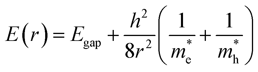 | (1) |
 | ||
| Fig. 1 (a) Splitting of energy levels in QDs due to the quantum confinement effect.22 Reproduced from ref. 22 with permission from Springer Nature. (b) MEG or impact ionization, (c) size-dependent energy levels for QDs; the semiconductor band gap increases with the decrease in the size of the nanocrystal, and (d) design of a QDSC, the magnified view represents charge generation, separation at PA and electrolyte interface upon illumination. | ||
In the above eqn (1), Egap is the bandgap of the semiconductor nanocrystal, ‘h’ is the Planck's constant, ‘r’ is the radius of the QD, and 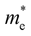 and
and 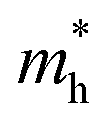 are the effective masses of the excited electron and hole respectively.
3. Fabrication of QDSCs
In a QDSC, a compact layer (blocking layer) of titanium oxide (TiO2) is applied on an FTO surface. In most cases, the compact layer is grown from an aqueous TiCl4 solution. This layer usually prevents direct contact between the electrolyte and the FTO surface. Over the compact TiO2 layer, a porous wide-band gap material such as titanium oxide (TiO2, most common) or zinc oxide (ZnO, rare) or tin oxide (SnO2, rare) is deposited which collects the photogenerated electrons from the photosensitizer QD after charge separation. In their bulk, the charge mobility for ZnO, TiO2, and SnO2 are 200, 1, and 250 cm2 V−1 s−1, respectively. Although the charge mobility is relatively low for TiO2 due to the LUMO position, it is the most commonly used wide bandgap semiconductor in QDSCs and photoelectrochemical cells.23 QDs are mostly metal chalcogenides with narrow band gaps, like CdS,24 CdSe,25 CdTe,26 CdSeTe,27 CdSeS,28 PbS,29 PbTe,30 Bi2S3,31 Bi2Se3,32 InS,33 InSe,34 InP,35 CuInS2,36 CuInSeS, etc.37 Besides QDs, Au nanoclusters38 and graphene39 have also been employed as light harvesters. Among hole scavengers, aqueous polysulfide is a widely used redox electrolyte in QDSCs.40 The iodine/tri-iodide redox couple is another hole scavenger, but it is predominantly used in DSSCs and not in QDSCs. This is because metal chalcogenide QDs dissolve in I2/I− solutions or gels and therefore, this redox couple is generally not used in QDSCs. Instead, either Na2S or polysulfide (S and Na2S) are used as electrolytes in QDSCs.41 The counter electrode (CE) in a QDSC reduces the polysulfide to sulfide (Sn2− to nS2−), and the CE also controls the QDSC performance. CE materials with a high electrocatalytic activity for the reduction of polysulfide or the oxidized electrolyte species are used. While Pt is the widely used CE in DSSCs, in QDSCs the polysulfide gets irreversibly deposited onto Pt, and it also corrodes Pt. As a consequence, other materials are used. Carbon materials such as functionalized multi-walled, single-walled carbon nanotubes (MWCNTs, SWCNTs),42 reduced graphene oxide (RGO),43 soot particles,44 and doped carbon materials,45 metal sulfides like PbS,46 NiS,47 Cu2S,48 Cu2S/RGO, and their composites,43 Cu2ZnSnS4,49 conducting polymers like polythiophene (PT), polypyrrole (PPy), and poly(3,4-ethylenedioxythiophene) (PEDOT)50 and metals like Pt,51 Au,17etc., are employed as CEs in QDSCs. However, several heterojunction QD based solar cells have been reported.52–544. Working principle of a QDSC
The working principle of a QDSC upon illuminating the cell involves three stages. In the first stage, exciton generation occurs. The second and third stages involve charge separation and regeneration of the QD by the electrolyte, preceded by electrolyte reduction at CE; in detail: when light impinges on the cell, electrons are excited from the HOMO to the LUMO of the QD, leaving holes in the HOMO (Fig. 1d). These photogenerated electrons are injected into the wide band gap semiconductor and are transmitted to the current collector (SnO2:F glass or FTO). These electrons pass through the load and finally reach the CE. In order to regenerate the oxidized QDs, the holes are scavenged by the reduced species redox couple, and the oxidized redox species in the electrolyte is reduced back at the CE. This is a continuous and cyclic process. The voltage, or the theoretical open-circuit voltage (Voc) generated by the cell under illumination, is determined from the difference between the oxide's Fermi level and the electrolyte's redox potential.55 The working principle for the QDSCs, QD synthesis and tethering methods, the several electrochemical phenomena, efficiency enhancement factors, and measurement principles are discussed in previous review articles.56–68Upon illumination
The inorganic QD typically has high absorptivity (106 cm−1).69| QD + hν → QD* [exciton: e− (LUMO), h+(HOMO)] (the electron will be excited to LUMO from the HOMO and leaves a hole behind in the HOMO). |
Change separation:
QD*[e−(LUMO), h+(HOMO)] + TiO2 → QD*[h+(HOMO)] (the electron from the LUMO of the QD, will be injected to the LUMO of TiO2).
QD regeneration:
QD*[h+ (HOMO)] + S2− → QD + S−˙ (the reduced electrolyte species will scavenge the hole from the HOMO of the QD).
Electrolyte reduction at CE
The more electrocatalytic the CE material is, the more efficient it will be in improving the PCE of a solar cell.70S−˙ + e− → S2− (the oxidized species in the electrolyte is reduced at the CE).
5. Synthesis of QDs
QD synthesis via solution processing is attractive because of the low cost and ease of synthesis. Some chemical methods such as hot injection, SILAR, and CBD are well known. In a one-pot or hot injection method,71 the metal powder or metal oxide is taken in a nonvolatile solvent with a high boiling point and heated to ∼200–350 °C. Once the metal precursor dissolves in the solvent, the solution turns clear. Without any delay, the chalcogenide precursor, which is taken along with a suitable long-chain organic capping agent, is rapidly injected under an inert atmosphere into the metal precursor solution. The nucleation of QDs begins. The QD size is controlled by the duration for which the reaction mixture is held at a high constant temperature. The QDs are collected by centrifugation and washed with methanol to remove excess ligands. The other popular method for QD fabrication is SILAR,72 an in situ method, where QDs such as CdS, PbS, ZnS, etc., can be deposited easily onto the wide bandgap semiconductor scaffold under ambient conditions. In this method, organic linker molecules or long-chain capping agents are not used. In the SILAR method, metal and chalcogenide precursor solutions are taken in two individual beakers. The substrate is initially placed in the metal precursor solution for a certain time, followed by rinsing in a solvent to remove the excess ions, which are not strongly adsorbed onto the wide band gap semiconductor. This substrate is then dried before it is placed in a second beaker of the chalcogenide precursor solution. The substrate is kept in the chalcogenide precursor solution simultaneously, and then it is rinsed in solvent and dried. This is known as one SILAR cycle for the deposition of QDs. The thickness of the QD deposit depends on the duration for which the substrate is immersed in the precursor baths and the number of SILAR layers employed. A very similar and another preferred method of QD synthesis is CBD.73 In this method, both the metal precursor and the chalcogenide precursor are taken in a single beaker and maintained at 70–80 °C, and the substrate is immersed in the solution for an appropriate time, and the metal chalcogenide deposit is obtained on the substrate. More information about QD synthesis and deposition techniques of QDs in QDSCs can be found in a previous review article cited here.74 The HOMO and LUMO positions and the bandgaps for individual semiconductor colloidal QDs are provided in Table 1.| Semi-conductor/insulator | Particle/QD size (nm) | Bandgap (eV) | HOMO (eV) | LUMO (eV) | Ref. |
|---|---|---|---|---|---|
| CdS | 5 | 2.3 | −6.2 | −3.9 | 75 |
| CdSe | 3 | 1.7 | −5.9 | −4.2 | 76 |
| CdSeS | 3–5 | 2.1 | −5.96 | −3.86 | 77 |
| CdTe | 3 | 1.54 | −5.04 | −3.5 | 78 |
| CdSeTe | 5 | 1.55 | −5.17 | −3.62 | 79 |
| PbS | 3–5 | 1.5 | −5.1 | −3.6 | 80 |
| PbTe | 2 to 7 | 1.07 | −4.9 | −3.83 | 81 |
| Bi2S3 | 4 | 1.54 | −5.7 | −4.16 | 82 |
| Sb2S3 | 5 | 1.65 | −5.4 | −3.75 | 83 |
| Sb2Se3 | 5 | 1.7 | −3.7 | −5.4 | 76 |
| In2S3 | 35 | 2.33 | −6.38 | −4.05 | 84 |
| In2Se3 | 5 | 1.35 | −5.79 | −4.44 | 85 |
| InP | − | 1.35 | −5.8 | −4.45 | 86 |
| Ag2S | 7 | 1.82 | −5.87 | −4.05 | 87 |
| Ag2Se | — | 1.71 | −3.15 | −4.86 | 88 |
| WS2 | 2 | 3.55 | −6.28 | −2.73 | 89 |
| WSe2 | 2.26 | −5.46 | −3.20 | 90 | |
| GaAs | — | 1.4 | −5.56 | 4.16 | 86 |
| GaP | — | 2.3 | −5.0 | −2.7 | 91 |
| CuInS2 (CIS) | 3 | 1.98 | −5.91 | −3.93 | 84 |
| CuInSe2 (CISe) | 4 | 1.49 | −5.04 | −3.55 | 92 |
| Cu–In–Ga–Se (CIGSe) | 3.5 | 3.63 | 4.86 | 1.23 | 82 |
| Zn–Cu–In–Se (ZCISe) | 4.1 | 1.58 | −4.58 | −3.27 | 93 |
| Cu2S | — | 1.8 | −5.9 | −4.1 | 94 |
| ZnS | — | 3.54 | −6.82 | −3.28 | 95 |
| ZnSe | 5 | 2.7 | −6.1 | −3.4 | 96 |
| ZnTe | — | 2.27 | −6.08 | −3.81 | 97 |
| C-dots | 5 | 3.61 | −7.13 | −3.52 | 98 |
| TiO2 | 20 | 3.2 | −7.25 | −4.05 | 99 |
| ZnO | 20–40 | 3.2 | −7.4 | −4.2 | 100 |
| SnO2 | 4 | 3.79 | −8.1 | −4.31 | 101 |
| MoO3 | 6 | 3.0 | −5.3 | −2.3 | 102 |
| WO3 | 90–100 | 3.15 | −7.3 | −4.15 | 103 |
| Al2O3 | 10–25 | 8.53 | −9.85 | −1.32 | 99 |
| SiO2 | — | 9 | −9.9 | −0.9 | 104 |
6. Defects at the photoanode/electrolyte interface and the importance of passivating layers
The PCE of liquid junction solar cells depends on charge-generation (retarded by the poor loading of QDs), charge-injection (retarded by the poor quality of interfaces), and charge-transfer (retarded by the charge trapping/non-radiative charge recombination (NCR)/back electron transfer to the electrolyte) processes. The poor charge collection efficiency was one of the major reasons for the low PCEs achieved for the earlier QDSCs. The intrinsic charge separation in the QD depends on the optoelectronic properties of the QD materials, whereas the charge transfer properties depend on QD crystal quality. The excessive recombination lowers the photocurrents and thus the PCEs for QDSCs. The reason for the poor charge collection efficiency is the serious charge recombination. The defect states in QDs cause recombination at the QD/TiO2/electrolyte interfaces. The initial low PCEs of the QDSCs were due to the poor charge-transfer properties, i.e., the charge trapping, NCR and back transfer of photogenerated electrons to the electrolyte. In QDSCs, the predominant charge trapping centers lie at grain boundaries and cracks in the form of surface/bulk defects over the PA where the photoelectrons get trapped, followed by NCR or back transfer. The latter possibly takes place at the trapping centers present over interfaces of (1) QDs/redox electrolyte, (2) electron transport layer (ETL)/QDs, and (3) ETL/electrolyte.105 In the PA, the thickness of the mesoporous ETL (e.g., TiO2) scaffold is in tens of micrometers, which works better than the thin-layered TiO2 (200 to 400 nm thick, which usually works for perovskite or solid-state solar cells) electrodes. Notably, the porous quality of titania plays a vital role and controls how efficient the QDSC is. Although the thick layer of ETL with a large surface area (50–100 m2 g−1) favors the high loading of QDs, the thick oxide will tentatively have a large number of cracks and grain boundaries, and eventually a greater number of defect sites.106 In the case of the low-temperature process of in-situ QD synthesis (CBD/SILAR) methods, the quality of the obtained QDs in terms of size and distribution will depend on protocols such as electrode dipping time inside the ion solutions, precursor concentrations, and the number of dipping cycles, etc.107 However, it results in the random size distribution of QDs, and adds charge transport resistance.108 Although such QDs suffer from poor crystallinity, since there are no insulating organic ligands coated over the QDs, charge injection to the TiO2 is relatively unhindered compared with bulk organic molecule capped QDs obtained from the pre-synthesis techniques. Considering the concepts like alloy/core–shell QDs, high-temperature QD pre-synthesis is the dominant QD synthesis approach according to the recent high PCE reports. QDs synthesized using high temperature or hot injection methods can possibly result in QDs with incomplete surfactants, causing dangling bonds to appear. Surface capping of QDs with bulky organic chains can also lead to charge isolation between the dots. At the same time, the greater number of terminated metal/chalcogenides without the capping creates electronic level misalignment at the interfaces of neighboring QDs and/or introduces additional electronic states near the HOMO/LUMO. Of course, at these defect sites, the low-lying energy levels can potentially serve as charge trapping centers. The photogenerated electrons will undergo NCR at these centers or allow the shunt paths inside the device.22,109 However, the other issue of overloading/poor-adsorption of QDs over PA results in PA instability, and bleaching of the PA. Thus, the resulting non-continuous film, non-uniform thickness, poor interface quality, in addition to the defects, grain boundaries, insulating barriers, lack of phase-purity, low crystallinity, pin-holes, and cracks are several factors responsible to poor charge transfer (Scheme 1). Therefore, ultimate solutions are (1) alloys of QDs, (2) QDs with overlayers (core–shell) of other semiconductors, (3) molecular treatments to the ETL/QDs, (4) a thin-layer coating of insulating/semiconducting materials on top of the PA, and (5) additives into the electrolyte; such passivation techniques can assist curing the above said charge trap centers present over the PA, and improve the solar cell conversion efficiency. | ||
| Scheme 1 Schematic illustration of the possible obstacles for the charge transfer process over a photoanode. | ||
Thus, the charge trapping centers on semiconductors at the QD/TiO2 and QD/electrolyte interfaces are severely responsible for back electron transfer (undesired shunt paths inside the device). From the above-said passivation methods, few effective ways have been developed to overcome these particular issues: (1) surface modification of the TiO2 electrode using Al2O3, SiO2, MgO, etc., namely, wide-band gap metal oxides. These act as energy barriers and lower the physical contact between the TiO2 and oxidized species in the electrolyte and retard their recombination. (2) ZnS, ZnSe, SiO2, or amorphous TiO2 (am-TiO2) passivation layers introduced onto the QD surfaces using SILAR to reduce the TiO2/QDs/electrolyte interfacial recombination processes. (3) Synthesis of alloy QDs, and (4) by the creation of aligned energy levels in PA for QDSCs, facilitating the separation of photogenerated electrons and holes, and thus leading to faster electron extraction and collection through the use of type-I or type-II QD core–shell structures (e.g., CuInS2/CdS, ZnTe/CdSe, CdTe/CdSe and CdS/CdSe QDs).
In most cases, it is found that the usage of alloy QDs (passivation of QDs) and coating a thin layer of insulating or wide bandgap material on PA (SILAR, PA passivation) together was found to be an effective approach to improve device performance. These layers are expected to buffer the QD/titania surface defects and prevent the QDs from peeling off from the PA/PA-bleaching. However, several other concepts upgrading the PA/QDs passivation methods reported will be discussed in detail.110–113
6.1 Passivation methods
The passivation methods are classified for ease of understanding, as represented in Fig. 2. | ||
| Fig. 2 Schematic illustrating the different passivation methods used for QDSCs: (a) the passivation of QDs by overlayer/alloying, (b) possible charge recombination/back transfer pathways with and without the passivation layers, and (c) passivation of PA by additive incorporation into the electrolyte and device performance. | ||
i. QD passivation methods such as overlayer (core–shell) and alloying (QD passivation)
ii. PA passivation methods such as a molecular layer or single/multiple layers (PA passivation)
iii. Passivation of PA through the additive incorporation in the electrolyte (electrolyte passivation).
As classified above, the information of multi-way passivation methods required to prevent PA corrosion (i.e., bleaching of PA, NCR, and back electron transfer to the electrolyte) are collected from the recently evolved literature and discussed below with suitable references.
 | ||
| Fig. 3 PL spectra evolved for CIS NCs when growing the (a) ZnS shell and (b) CdS shell. (c) The lowered decay for CIS NCs after overcoating with the CdS layer and (d) overcoating with the ZnS layer reduces the contribution from the fast decay channel. Reprinted with permission from ref. 114. Copyright {2011} American Chemical Society. | ||
The thin passivating layer can be reactive with the QDs during the synthesis, reported as “shelling and alloying effects”. In this case of passivation, it is not only the physically adsorbed top layer but involves tuning of the semiconductor composition notably and thus the optoelectronic properties. The shelling/alloying of the QDs is expected to passivate surface defects, enhance their emission properties and result in improved device PCE. To date, the highest reported efficiency of 15.3% comes under the category of an alloying effect. However, the author has demonstrated a duel layered QD loading onto TiO2. Before the second layer, an Mg(OH)x treatment is done to the PA, which acts as a passivation layer responsible for the increased QD loading.8 Bose et al. discussed the effect of alloying behavior during the ternary NCs passivation by ZnS/Se. The roles of passivation by the ZnS layer and alloying effects over NCs were understood from the PL-lifetime measurements. Ternary alloy NCs such as CIS, CuInSSe (CISSe, where the S:Se ratio is 0.7:0.3), and CuInSe2 (CISe, where the S:Se ratio is 0.15:0.85 and the S originates from dodecanethiol) were synthesized and coated with a ZnS overlayer. With Se, the authors observed red-shifts in absorption and emission spectra. ZnS's further coating resulted in a blue shift caused by the large bandgap of ZnS and the reduced defect states on the NCs. When the emission of the NCs without and with the ZnS overlayer was studied, the QY for CIS, CISSe, and CISe were found to increase from 12.04, 11.72, and 8.51% to 70.67%, 63.54, and 51.73%, respectively. Using inductively coupled plasma optical emission spectroscopy (ICP-OES), the authors observed that the ZnS's mole percentage in the NCs after shelling with ZnS was ∼20% of the total prevailing cations. Transient absorption measurements were used to study the carrier lifetimes (from the ground-state bleach recovery) before and after shelling with ZnS. Two time components in the ranges of 5–8 ns and 73–125 ns were observed for all three NCs. But, after shelling with ZnS, the relative amplitude of the fast component was found to be reduced. Shallow electron trap states were ascribed to S/Se vacancies present on/near the NC surfaces, and the ZnS shell eliminated these. Deep electron trap states originated from the In–Cu substitution defects, which also vanished after the diffusion/alloying of Zn–ions into the NC structure.115
In another report, Peng et al. constructed a QDSC based on a “simultaneous nucleation and growth” approach. Herein, a Ga-element was introduced into the CISe host to form the Cu–In–Ga–Se (CIGSe) QDs, which allowed tailoring of the electronic structure based on the higher bandgap Cu–Ga–Se (1.65 eV) system. The CIGSe quaternary material exhibited an ideal bandgap for solar conversion, and a Jsc > 25 mA cm−2 was achieved (Fig. 4). The CIGSe//titanium mesh supported mesoporous carbon (MC/Ti) CE based QDSC exhibited a high PCE of ∼11.5% (Jsc = 25.01 mA cm−2, Voc = 0.740 V, FF = 0.621) under one sun irradiation, contrasting with 9.46% for CISe//MC/Ti QDSC. PCEs of 9.34% and 7.65% were achieved for the best CIGSe and CISe QDSCs with Cu2S/brass CE. Average electron lifetimes (τav) for CISe and CIGSe QDs deposited over SiO2 varied in the order of CIGSe (47.48 ps) > CISe (18.40 ps). These results indicated that charge recombination was better suppressed in process CIGSe alloy QDs than in CISe QDs. Open circuit voltage decay (OCVD) and electrochemical impedance spectroscopy (EIS) analysis also revealed that intrinsic recombination in CIGSe QDSCs was well suppressed relative to CISe QDSCs.82
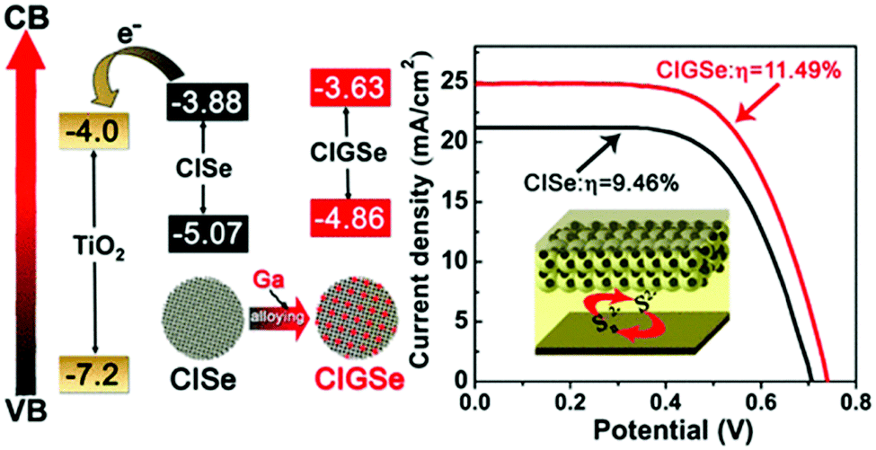 | ||
| Fig. 4 Energetics favorable for charge collection and the J–V curves obtained for the QDSC constructed using Ti-mesh supported mesoporous carbon CE. Reprinted with permission from ref. 82. Copyright {2017} American Chemical Society. | ||
6.1.1.1 Core–shell type passivation for QDs. CdSeTe/CdS is a type-I core–shell structure, wherein the CdSe0.65Te0.35 (simplified as CdSeTe) serves as an ideal core QD, and the CdS shell was coated around it to decrease and increase the surface defect density and the stability of the core QD respectively. By adjusting the thickness of the CdS shell, the PCE of the CdSeTe/CdS–QDSC was 8.02%, and it was increased by 13% in comparison to that of CdSeTe–QDSC, which showed a PCE of 7.1%. Transient absorption (TA), incident photon to current efficiency (IPCE), OVCD, and EIS measurements verified the suppressed charge recombination process in the QDs and QD/TiO2/electrolyte interfaces after coating the CdS shell around the CdSeTe core QDs. Further coating of overlayers of amorphous(a)–TiO2 and SiO2 barrier films over the QD@PA led to a PCE of 9.48% for the champion cell.116Fig. 5a also illustrates the physical barrier: the CdS shell on top of the alloyed QD core with an appropriately positioned LUMO level that prevents: (i) charge recombination and (ii) back electron transfer to the hole transporting electrolyte.
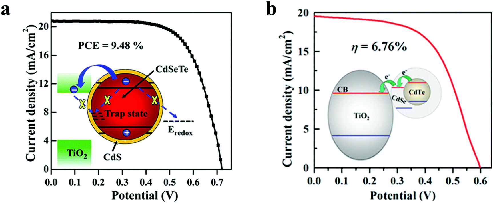 | ||
| Fig. 5 (a) CdSeTe/CdS Type-I core–shell, and (b) CdTe/CdSe type-II core–shell QD sensitizer. Reprinted with permission from ref. 116 and 117. Copyright {2015} {2013} American Chemical Society. | ||
In another report, Zhong's group employed CdTe/CdSe type-II core–shell QDs and showed the possibility of converting a broad portion of the absorption spectrum to electricity. Besides this, the system allowed rapid charge separation and offered low charge-recombination rates.117 The authors achieved higher absorption of solar radiation due to the PA design, i.e., the high QD loading and the inherently better optoelectronic characteristics of type-II core–shell QDs (wide absorption range, fast charge separation, and slow charge recombination). The CdTe/CdSe QD based sandwich solar cell showed a PCE of 6.76%. In the type-II core–shell, the CdTe/CdSe QD extended light-absorption range to the infrared (IR) region was achieved owing to an exciplex state formed between the HOMO of CdTe and the LUMO of CdSe. Type-II CdTe/CdSe core–shell QDs are superior to sole CdSe QDs for the former offered the following benefits: (1) wider light-harvesting region with the absorption onset in the IR domain, an accelerated electron injection rate, and a retarded recombination rate induced by the spatial separation of the exciton in the type-II QD. In Fig. 5b, the inset schematic shows how the aligned LUMOs, favor electron injection to TiO2via relay.117
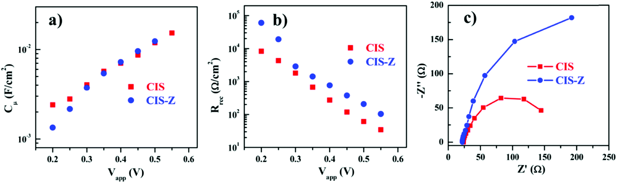
In 2014, Pan et al. fabricated a solar cell containing type-I core–shell CuInS2/ZnS QDs. Solar cells based on “green” QDs totally free of Cd or Pb to develop green QD solar cells were constructed. The LUMO edge position or the density of the states of TiO2 were said to be unaffected for both QDSCs with and without ZnS passivation on PAs. Using the wide absorption range QDs, CuInS2/ZnS (CIS-Z) based QDSC achieved a PCE of 7.04%. This was only 5.05% when the ZnS shell was not applied over the CuInS2 (CIS) QDs. The reason behind the enhanced PV performance was predicted by the comparison of EIS results obtained for CIS-Z and CIS QDSCs. The chemical capacitance (Cμ) and recombination resistance (Rrec) values as a function of applied bias are provided in Fig. 6. A higher Rrec value (3-fold enhancement) was obtained for the CIS-Z based QDSC compared to the CIS QDSC at a forward bias of −0.55 V. Since both the QDSCs were fabricated under identical conditions, the enhanced recombination resistance for CIS-Z was ascribed to the ZnS effect as an electron blocking layer at the TiO2/QD and PA/electrolyte interfaces. The electron lifetime (τn = Rrec × Cμ) for the CIS-Z cell under open-circuit condition was found to be ∼3-fold times longer than that obtained for the CIS based QDSC, which was ascribed to the improved charge collection.118
 | ||
| Fig. 6 EIS characterization plots obtained for CIS-Z and CIS based QDSCs: (a) chemical capacitance Cμ values, (b) recombination resistance Rrec, and (c) the Nyquist plots. Reprinted with permission from ref. 118. Copyright 2014 American Chemical Society. | ||
6.1.2.1 Molecular-/single-layer passivation. The photogenerated electrons trapped at defects will tend to recombine largely with the holes present at low-lying energy states (of QDs) or transfer back into the electrolyte before the charge collector collects them. The defects will be cured when molecular solutions can treat the surface of defected TiO2 nanoparticles instead of forming a compact layer. In the QDSC fabrication process, generally, the mesoporous and thick TiO2/FTO film is usually subjected to TiCl4 aqueous solution treatment. Incomplete surface oxidation leaves the surface oxygen-deficient, which serves as the trap state. Thus, our group has focused on preventing TiO2 surface/sub-surface defects by carbonate (CBN) treatment for effective charge collection from the QDs. After treating with the CBN, the TiO2 electrodes were used for the construction of large-area QDSCs as well (Fig. 7). Notably, a wider optical bandgap, a lowered fluorescence intensity (compared to the strong emission due to the defects present in untreated TiO2), and XPS data delineated a lowered proportion of Ti–OH in treated TiO2 that the simple treatment works very well. Emission decay studies further revealed that the average electron lifetime improved from 2.2 ns (without CBN treatment) to 8.8 ns for TiO2–CBN when the emission decay was monitored at 430 nm. This confirmed the reduced defect densities in the CBN treated TiO2 based PA. In order to further evaluate the surface passivation behavior of CBN: both, with and without CBN treated TiO2 film based PAs were employed for QDSC fabrication following identical conditions. This report studied different active-area PAs, and the best PCE achieved with the CdS QDs based QDSC with an active area of 0.3 cm2 is 6.3% with the CBN treated PA. In contrast, the QDSC PCE increased from 3.03% (TiO2 film without CBN treatment) to 4.32% (TiO2 film with CBN treatment) for QDSCs, whose PA active-area was 1 cm2. Thus, in this work, the effectiveness of the CBN treatment that resulted in a distinctively superior QDSC performance was demonstrated through detailed analysis.122
 | ||
| Fig. 7 Schematic showing the changes in TiO2 induced by CBN treatment: the photographs of QDSC with larger-area, lightened LED with three QDSCs connected in series under illumination. Reprinted with permission from ref. 122. Copyright 2017 American Chemical Society. | ||
Though wide bandgap materials are mostly used for the passivation layers, narrow bandgap for passivation could play a vital role in directing the photoelectrons. However, narrow bandgap passivation with the conduction band alignment against the light sensitive QDs will concentrate the electron density besides acting as a buffering layer for surface traps. In a report by Chang et al., a CuInS2 based QDSC was fabricated with a multilayered architecture by the SILAR method. Different metal chalcogenides as interfacial buffer layers were employed to improve the unmatched band alignments between the TiO2 and CuInS2 QDs, which resulted in improved Jsc and Voc for the CuInS2 based QDSC.123 Proper band alignment at the hetero-interface and the negative band edge shift of TiO2 were responsible for the improved solar conversion response (Fig. 8). The hybrid-containing cells were characterized by PCEs that were 1.3 times larger than the cells with identically pre-treated In2Se3 interfacial buffer layers. In addition, they established that ZnSe functioned as a good passivation layer over the CuInS2/CdSe hybrid-sensitized QDs, inhibited current leakage from the QDs to the electrolyte, and decreased the interfacial charge recombination. Finally, the QDSCs delivered a maximum external quantum efficiency (EQE) of 80% at 500 nm and the highest PCE of 4.55%, roughly nine times greater than that of the QDSC containing sole CuInS2.
 | ||
| Fig. 8 Schematics representing (a) a layer-by-layer deposited TiO2, QDs, and passivation layers in the PA in a QDSC and (b) energy-level diagrams of CuInS2/CdS, CuInS2/CdSe, and CdSe/CuInS2. Reprinted with permission from ref. 123. Copyright {2013} American Chemical Society. | ||
In most of the articles, the high PCE values that are reported are largely for cells with PAs passivated by a ZnS layer (can be seen in the year-wise best PCE reports, Table 2). However, layer by layer passivation of ZnS, SiO2, and a-TiO2 or all-together has improved the QDSC efficiencies more effectively.
| PA | Passivation layer/type | Counter electrodes (CEs) | V oc (mV) | J sc (mA cm−2) | FF (%) | η (%) | Year [ref.] |
|---|---|---|---|---|---|---|---|
| TiO2/CdSe | ZnS/(SILAR) | Cu2S/Brass | 561 | 16.96 | 56.6 | 5.42 | 2012139 |
| TiO2/CdSe | ZnS/(SILAR) | Cu2S | 579 | 15.77 | 56.95 | 5.21 | 2012140 |
| TiO2/CdSe/CdS/ZnS | ZnS/(SILAR) | Cu2S/Brass | 527 | 18.02 | 56.0 | 5.32 | 2012141 |
| TiO2/Mn-d-CdS/CdSe | ZnS/(SILAR) | Cu2S–graphene oxide | 558 | 20.7 | 47.0 | 5.42 | 201218 |
| ZnO/ZnSe/CdSe | ZnSe/(SILAR) | Cu2S–graphene oxide | 761 | 17.3 | 47.1 | 6.20 | 2013142 |
| TiO2/CdTe/CdSe | ZnS/(SILAR) | Cu2S/brass | 606 | 19.59 | 56.9 | 6.76 | 2013117 |
| CuInS2 | ZnS/(SILAR) | Cu2S/brass | 586 | 20.65 | 58.1 | 7.04 | 2014118 |
| TiO2/CdSexTe1–x | ZnS/SiO2/(SILAR) | Cu2−xS/FTO | 656 | 20.71 | 61.6 | 8.37 | 2015124 |
| TiO2/Mn:QD/Mn:ZnS/SiO2 | Mn:ZnS/(SILAR) | Cu2S/brass | 688 | 20.87 | 65.5 | 9.40 | 2016143 |
| TiO2/CdSeTe | ZnS/SiO2/(SILAR) | Cu1.8S-C/FTO | 655 | 21.27 | 60.0 | 8.4 | 2016137 |
| TiO2/CdSeTe | ZnS/SiO2/(SILAR) | Cu2S/brass | 710 | 22.21 | 71.2 | 11.23 | 2016130 |
| TiO2/CdSeTe | a-TiO2/ZnS/SiO2/(SILAR) | Ti-mesh/mesoporous carbon (Ti-MC) | 803 | 20.67 | 68.6 | 11.39 | 2016144 |
| TiO2/ZnCuInSe (ZCISe) | ZnS/SiO2/(SILAR) | Ti-MC | 745 | 25.49 | 62.7 | 11.91 | 2016145 |
| TiO2/CdSeTe | a-TiO2/ZnS/SiO2/(SILAR) | Ti-mesh/graphene hydrogels (GHs) | 786 | 20.69 | 66.02 | 10.74 | 2017146 |
| TiO2/Cu–In–Se and Cu–In–Ga–Se | ZnS/SiO2/(SILAR) | Ti-MC | 740 | 25.01 | 62.1 | 11.49 | 201782 |
| TiO2/ZnCuInSe (ZCISe) | ZnS/(SILAR) | N-Doped mesoporous carbon (N-MC) | 758 | 25.53 | 63.2 | 12.23 | 2017147 |
| TiO2/ZCISe | ZnS/(SILAR) | Cu2S/brass | 752 | 25.97 | 64.4 | 12.57 | 2017148 |
| TiO2/CdSeTe | ZnS/SiO2/(SILAR) | CNT@rGO@MoCuSe | 633 | 20.54 | 63.6 | 8.28 | 2018149 |
| TiO2/ZCISe | ZnS/SiO2/(SILAR) | Cu2S/brass | 629 | 26.58 | 61.0 | 10.2 | 201893 |
| TiO2/ZCISe/CdSe | ZnS/(SILAR) | MC/Ti | 752 | 27.39 | 61.9 | 12.75 | 2018150 |
| TiO2/ZCISe/ZCIS | Overlayer on QDs | MC/Ti | 763 | 26.09 | 66.2 | 13.18 | 2019151 |
| TiO2/ZCISe | ZnSSe/(SILAR) | Ti-MC | 733 | 26.49 | 68.52 | 13.3 | 2019152 |
| TiO2/ZCISe | ZnS/(SILAR) | N-MC/Ti | 764 | 27.38 | 64.2 | 13.43 | 2019153 |
| TiO2/ZCISe | ZnS/(SILAR) | Co, N–C/Ti-mesh | 787 | 25.75 | 67.8 | 13.74 | 2019138 |
| TiO2/ZCISe | ZnS/(SILAR) | Graphene hydrogel (GH-Cu2S/Ti | 770 | 26.49 | 67.9 | 13.85 | 2019154 |
| TiO2/Al0.5Zn0.5–CuInSe | ZnS/(SILAR) | Cu2S/brass | 620 | 27.15 | 61.0 | 10.27 | 2020155 |
| TiO2/ZCISe/ZnSe | Overlayer on QDs | N-MC/Ti | 780 | 26.7 | 66.4 | 13.84 | 2020156 |
| TiO2/ZCISe | ZnS/(SILAR) | N-MC/Ti | 777 | 26.97 | 66.47 | 13.93 | 2020129 |
| TiO2/Zn0.4Cu0.7In1.0SxSe2−x (ZCISSe) | Alloyed QDs | N-MC | 781 | 25.76 | 72.0 | 14.48 | 2020157 |
| TiO2/ZCISSe/Mg/ZCISSe | ZnS/(SILAR) | NMC/Ti | 789 | 24.23 | 70.8 | 15.2 | 20218 |
6.1.2.2 Double layer passivation. Zhao et al. employed a sequential inorganic ZnS/SiO2 double layer treatment onto the PA to inhibit the interfacial recombination processes in QDSCs.124 According to the authors, interfacial recombination for QDSCs can be restricted by using a barrier layer before or after sensitization. Suppose the passivation is carried out before or after the adsorption of QDs onto TiO2. In that case, it will affect the electron-transfer (ET) rate to the oxide or hole transfer rate to the electrolyte, respectively. It also provides stability to the QDSC (e.g., by protecting QDs from potential corrosion by the electrolyte). To unravel aspects related to PA passivation, a ZnS/SiO2 double-barrier coating was sequentially deposited after QD sensitization on the PA in QDSCs (for both CdSe- and CdSexTe1−x based cells, Fig. 9). The influence of this treatment was also analyzed through theoretical simulations, and its effect on charge transport and transfer at the QD/oxide interface were discerned from impedance and THz spectroscopy. Using theoretical modeling and EIS, they studied the reduced interfacial recombination and increased charge collection efficiency for combined ZnS/SiO2 treatment and compared it with conventional ZnS treatment alone. Finally, the CdSexTe1−x QDSC exhibited a PCE of 8.21% and improved cell stability with this double layer passivation effect. The mechanism of inorganic double oxide layer passivation was understood from density functional theory (DFT) calculations. The ZnS/SiO2 layer deposited onto TiO2 (101) was studied in detail. The TiO2 surface gets passivated via the formation of ordered Zn–O and S–Ti bonds that saturate all the dangling bonds. Moreover, the double barrier coating with SiO2 over ZnS resulted in Si–S and O–Zn bonds at the SiO2/ZnS interface that eliminated all the exposed S and Zn surface atoms. As anticipated, the cells showed better stability since the thick ZnS layer coupled with the SiO2 barrier layer inhibited photo-corrosion of chalcogenides under exposure to polysulfide and illumination.
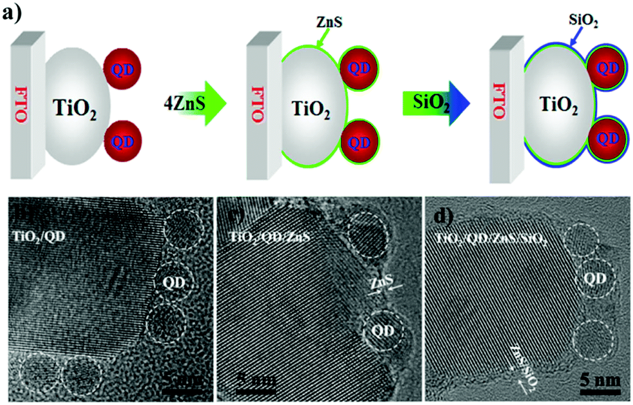 | ||
| Fig. 9 (a) Schematic representing the step-wise depiction of PA passivation, (b) HRTEM images of CdSeTe QDs deposited over TiO2, (c) ZnS layer over-coated, and (d) ZnS/SiO2 over-coated CdSeTe QD-TiO2 films. Reprinted with permission from ref. 124. Copyright {2015} American Chemical Society. | ||
In a previous study, CdSeTe QD-based PA was used in a QDSC, and the open-circuit voltage (Voc) obtained was 0.64 V. The Voc value was low compared to the QD's optical band gap of ∼1.5 eV. Passivating the PA surface states to reduce charge recombination is the most straightforward strategy for improving the photovoltage. Based on this concept, the authors modified the surface of TiO2 particles and QDs with an amorphous (am)-TiO2 layer and observed the enhanced effectiveness of a recombination blocking ZnS/SiO2 barrier layer.125
In a classical approach, the am-TiO2 is grown from an aqueous TiCl4 solution (TiCl4 hydrolysis followed by sintering at high temperature (typically at 400–500 °C)) during or onto the preparation of the TiO2 electrode. This is followed by the QD adsorption. The am-TiO2 layer can significantly improve the photocurrent of the QDSC due to the suppression of charge recombination owing to the decreased surface traps in the ET TiO2 layer. It also increases the interconnectivity of TiO2 particles on the electrode and allows increased loading of QDs. The authors, however, presented the additional application of am-TiO2 as a passivation/buffer layer that can be sandwiched between the QD sensitized PA and the ZnS/SiO2 barrier layer to decrease the trap state defects induced by the large lattice mismatch between the interfaces. This resulted in suppressed charge recombination and thereby enhanced QDSC performance. To attain a clear picture of this am-TiO2 passivation behavior on PAs, the authors have studied the same by applying it between different interfaces. It was found that am-TiO2 has a large effect on performance when it is situated between the sensitized PA and the ZnS/SiO2 barrier layer interfaces. It enhanced the photovoltage of the QDSC compared to the am-TiO2 layer located at other positions (i.e., in-between the ZnS and SiO2 layers or above the ZnS/SiO2 layer).
When the am-TiO2 passivation layer was incorporated between the sensitized PA and ZnS/SiO2, the photovoltage was 0.702 V. Without this layer, it was 0.638 V. Experimental data also affirmed that by just using the am-TiO2 layer, a large PCE improvement could not be affected. It was concluded that the synergy between the am-TiO2 and ZnS/SiO2 barrier layers leads to a high PCE. EIS and OCVD measurements demonstrated that the am-TiO2 passivation layer reduced the electron recombination at the PA/electrolyte interface to a great extent, whereas the other energetic features of the PA, such as the LUMO level, remained unaffected. Electron lifetime was found to be prolonged by several times. The ensuing QDSC with the QD/am-TiO2/ZnS/SiO2 PA benefited from all of the above features and exhibited a PCE of 9.28% (Fig. 10).
 | ||
| Fig. 10 (a) Schematics for the sequentially deposited passivation of ZnS, SiO2, and am-TiO2/ZnS/SiO2 on PAs. (b) Certified J–V curves were obtained for QDSCs. Reprinted with permission from ref. 125. Copyright {2015} American Chemical Society. | ||
6.1.3.1 Polyethylene glycol (PEG) additives. In 2015, Zhong et al. fabricated a CdSe QDSC with Cu2−xS/FTO as CE and a polysulfide electrolyte modified with the PEG as an additive.128 Many QDSCs with different PEG concentrations in the electrolyte were fabricated to discern the PEG effect under identical cell fabrication conditions. A gradual increase in PCE was registered when the PEG concentration was increased from 0 to 15 wt%, as shown in Fig. 11. Increased FF and Voc caused the PCE increase, but the Jsc was found to be largely invariant over the said PEG concentration range. EIS and OCVD data analysis delineated that the Rrec values improved with PEG addition. The Voc decay rate in the dark was also found to be slower for the PEG-polysulfide-based solar cell compared to the cell without PEG. PEG decreased the recombination rate for the photogenerated electrons with the oxidized moiety in the electrolyte. Stability tests under continuous irradiance for QDSCs with and without PEG showed that for both the QDSCs, the PCE values increased in the first two hours, and this phenomenon was attributed to the electrolyte penetration into the PA. But for prolonged illumination times, the QDSC without PEG was reduced by 80% of its initial PCE, whereas for the QDSC with PEG, the PCE remained the same until after 35 hours of continuous irradiation.
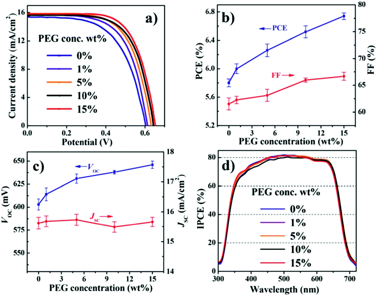 | ||
| Fig. 11 PV characterizations done for QDSCs with different concentrations of PEG in the electrolyte: (a) J–V measurements, (b) PCE and FF comparison, (c) Voc and Jsc comparison, and (d) IPCE. Reproduced from ref. 128 with permission from the Royal Society of Chemistry. | ||
In 2018, the influence of the molecular weight (Mw from 300 to 20000) of PEG in the electrolyte was investigated by Zhong's group. It is found that with low Mw PEG-300 polymer addition, the QDSC works efficiently (PCE, 10.2%) when compared to the other PEGs-1k,4k, and 20k Mws.93 Zhong et al. also studied the other hole transport layers (HTL) on top of PAs in 2020. To enhance the hole scavenging property, before assembling the cell, the PAs were immersed into HTL solutions of graphene oxide (GO), diphenyl sulfide (DPS), and 2,20,7,7-tetrakis[N,N-di(4-methoxyphenyl)-amino]-9,90-spiro-bifluorene (Spiro)), respectively. However, the PCE was found to be superior for GO immersion (13.84%).129
6.1.3.2 Fumed SiO2 modified electrolytes. Fumed silica (SiO2) nanoparticles (NPs) are stable for electrochemical and photochemical reactions. Meng et al. introduced SiO2 NPs as an additive into a polysulfide electrolyte and used them in the CdSexTe1−x based QDSC.130 With the modified electrolyte containing the optimized SiO2, improved PCE and QDSC stability was achieved. The authors predicted the effect of SiO2 as a passivation layer over the PA and elucidated its influence from EIS measurements. The fumed SiO2 NPs formed an insulating barrier between TiO2/CdSexTe1−x PA and electrolyte and prevented the back electron transfer. CdSexTe1−x QDs decorated TiO2 PA, polysulfide electrolytes with and without SiO2, and a Cu2S CE were assembled into sandwich-type QDSCs. For the cell without SiO2, a PCE of 8.73%, and a Voc of 643 mV, were obtained. But, when SiO2 (3 wt%) was introduced into the polysulfide electrolyte, the PCE and Voc improved to 11.23% and 710 mV. However, upon further increasing the amount of SiO2, the PCE dropped to 8.97%, indicating that too much of the SiO2 additive is unfavorable to cell performance. The improved cell performance and stability with the addition of SiO2 are shown in Fig. 12. To evaluate the influence of electrolyte additives on the electrochemical behavior, three devices were constructed following identical conditions with conventional polysulfide as a reference cell and with PEG and SiO2 additives for the QDSC. From the fitting parameters, the electron lifetimes were calculated for the three sets of QDSCs: a longer lifetime of 180 ms was achieved with SiO2 additive with suppressed charge recombination at the PA and electrolyte interface, compared to the conventional electrolyte (101 ms) and PEG-based electrolyte (118 ms).
 | ||
| Fig. 12 (a) Schematic representation of the role of the SiO2 electrolyte additive, which also serves as a physical barrier for the prevention of charge recombination between PA and electrolyte. (b) Stability test done for both QDSCs with and without the SiO2 electrolyte additive. Reproduced from ref. 130 with permission from the Royal Society of Chemistry. | ||
From our group, Das et al. studied the influence of modified SiO2 gel electrolyte after the addition of a polyanionic sodium poly(4-styrenesulfonate) (NaPSS), which acted as a passivation layer, enabled by the Coulombic interactions between negatively charged sulfonate groups on the polymer chain and the positively charged metal atoms such as Ti4+/Cd2+ over PA. The enhanced penetration also improved the hole scavenging ability of the electrolyte into the PA.131 In detail, for the fabrication of the QDSC, a combination of nitrogen-doped graphene particles (NGPs) and CdS QDs tethered to TiO2 was used as the PA. On the other side, carbon-cloth coated with poly(3,4-ethylenedioxypyrrole) (PEDOP) was employed as an effective CE. EIS studies showed that PSS formed a barrier layer on the PA and provided additional back electron transfer resistance at the PA/electrolyte interface when compared to the sole SiO2 additive. A PCE of 7.7% was achieved for the champion device with the best FF value of 78%.
7. Importance of counter electrodes for high-efficiency QDSCs
CE is one of the key components, and its catalytic activity and charge transfer resistance are the efficiency deciding factors for QDSCs. The best CEs for high-efficiency QDSCs should have high catalytic activity to reduce the oxidized electrolyte species and a low charge transfer resistance for electron transfer at the CE/electrolyte interface. In QDSCs, the most commonly used redox couple is sulfide or polysulfide (S2−/Sn2−), which scavenges holes from the QDs more efficiently than other redox couples like Fe2+/Fe3+ or I−/I2−. CE should also have a high effective surface area, good chemical and photochemical stability, and optical transparency for building integrated, tandem, smart solar cells. Several materials have been employed as CEs in DSSCs to attain maximum PCE,132 and platinum metal (Pt) is the most popular. Despite its efficient charge transfer kinetics during the reduction process, its poor affinity towards S2− and its tendency to dissolve in the alkali render it less effective for QDSCs. Alternatively, metal sulfides, carbon nanostructures, hetero-atom doped metal oxides, and conducting polymers came into the picture.133,134 Several review articles have reported different CE materials synthesis, usage and characterization for DSSCs, and QDSCs.132,135 From our group, Naresh et al. studied the influence of CEs on the performance of CdS QD-based solar cells. With the ideal fabrication conditions, the charge transfer resistance for a set of CEs was found to be different and reflected the same on their PCEs.136 To fabricate the Cu–carbon composite@FTO CE, a paste of commercial copper powder, activated carbon (AC), and carbon black (LUMO) was screen printed on FTO (Fig. 13). Furthermore, Cu1.8S–C hybrid CEs were constructed by sulfidation of the Cu–carbon composite@FTO in a polysulfide solution. The assembled CdSeTe-sensitized QDSC achieved a PCE of up to 8.40%, higher than pure carbon CE (5.25%) and comparable to that obtained with traditional Cu2S/brass-based CE (8.44%).137 The strong and uniform anchoring of Cu1.8S particles improved the catalytic activity for polysulfide reduction and induced the improved PCE. | ||
| Fig. 13 Synthesis process of Cu1.8S-C CEs, and the best PCE curve obtained for the QDSC. Reprinted with permission from ref. 137. Copyright {2016} American Chemical Society. | ||
To enhance the performance of QDSCs with a carbonaceous material-based CE, doping with nitrogen hetero-atoms, which get incorporated into the carbon lattice, is an efficient way to enhance the catalytic activity towards electrolyte reduction. Zhong's group doped mesoporous carbon with nitrogen (N-MCs) and used it as a CE in Zn–Cu–In–Se QDSCs. Doping N into the graphitic structure alters the lattice's local symmetry and increases edge-plane defect sites, which reduce the polysulfide more actively. During the synthesis, the ratio of melamine to phenol was varied, and N-MCs with different contents of N were achieved (2.89, 4.76, and 8.58%). The N-MC samples were screen printed on Ti-mesh from a paste and used as CEs in QDSCs. At an N content of 8.58 wt%, the cell with an N-MC/Ti-CE exhibited the highest PCE of 12.23% and a certified PCE of 12.07%. Contrasting with the undoped MC/Ti CE-based cell, the one with N-MC/Ti CE showed a substantially increased FF. The average PCE increased from 11.44 to 12.23% from MC/Ti to the N-MC/Ti CE.45 EIS data for four different CEs, including different and no N content-based ones, were examined. Nyquist plots are shown in Fig. 14. The two semi-circles were attributed to the (doped or undoped) carbon/Ti and CE/electrolyte interfaces. On raising the N content from 0% to 8.58%, the RCT decreased from 2.2 to 0.94 Ω cm2, thus favoring the cell response. Tafel plot analysis showed that the increased current density with increasing N-content reflected the improved catalytic behavior for the doped carbon. Cyclic voltammetry data also reaffirmed this trend, where the reductive current densities were high with N in the MC lattice.
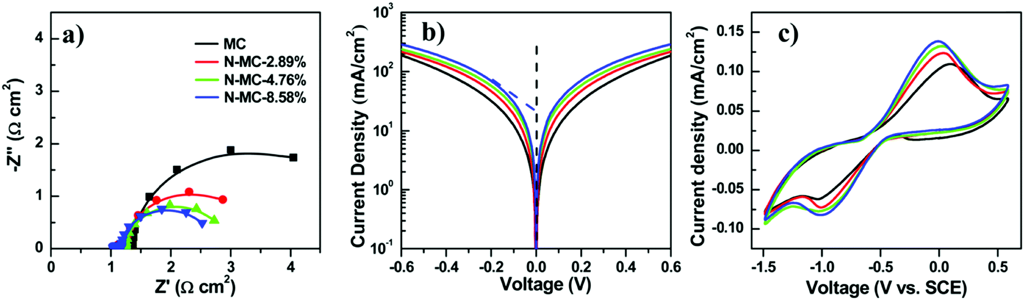 | ||
| Fig. 14 Electrochemical properties of CEs with different amounts of nitrogen in N-MCs. (a) Nyquist plots, (b) Tafel polarization curves, and (c) cyclic voltammograms. Reprinted with permission from ref. 45. Copyright {2017} American Chemical Society. | ||
Most of the reported high-efficiency liquid junction solar cells have CEs based on either Cu2S or MC-Ti-mesh electrodes, as referred to above. Table 2 summarizes PV parameters of different liquid junction QDSC architectures having different CEs. But with the idea of increased surface area and catalytic centers, Co, N–C coated Ti-mesh CE was also developed for high-efficiency QDSCs. The hetero atom doped carbon paste was prepared from a metal–organic framework (MOF) as shown in the schematic (Fig. 15). Layered double hydroxide (LDH) nanosheets were first synthesized using a hydrolysis method and applied as a sacrificial scaffold template. Cobalt–zeolite-imidazole framework (ZIF-67) crystals were grown on both sides. After high-temperature carbonization at 800 °C in an Ar atmosphere and acid treatment, Co–N-co-doped porous carbon composite (Co, N–C) with a honeycomb structure was obtained with a surface area of 489 m2 g−1. The obtained Co, N–C was applied onto the Ti-mesh and utilized as the CE in a Zn–Cu–In–Se (ZCISe) QDSC. The average PCE was 13.55%, a ∼10% enhancement over its analogue with an N-MC CE-based QDSC. The lowered Rct values for the Co, N–C/Ti mesh CE indicates increased active catalytic sites in Co, N–C, which facilitated the regeneration of QD from its oxidized state. The unique structure of Co, N–C facilitated the reduction ability of Sn2− to S2−, by lowering the reaction barrier for this process. The honeycomb-like structure and sheet-like shapes were characterized by large-sized pores that promoted deep electrolyte permeation, thereby establishing good contact between the electrolyte and the active catalytic centers. The larger current densities achieved for polysulfide reduction in the Tafel and CV data analysis for Co, N–C/Ti-mesh also confirmed its higher catalytic activity than N–C/Ti-mesh.138
 | ||
| Fig. 15 (a) Schematic illustrating the step-wise synthesis of a Co, N–C composite. SEM images of (b) CoAl-LDH, (c) CoAl-LDH@ZIF-67, and (d) Co, N–C. Reprinted with permission from {138}. Copyright {2019} American Chemical Society. | ||
8. Perspective
Attainment of a good trade-off between stability (shelf and operational life) and PCE is a key issue in solution processed QDSCs that needs to be further addressed not just by the implementation of passivation methods for restricting photocorrosion but also exploring non-aqueous yet inexpensive redox electrolytes (used as the hole transport materials (HTMs)) to overcome the limitations of evaporation of solvent, turbidity, leakage and showing no compositional change under the effect of UV light and high temperature. Superior QDs that offer low toxicity and are environmentally friendly, with a wider absorption range and higher light-harvesting capacity, must also be investigated in the future to extend the shelf-life of QDSCs without compromising their photovoltaic performance. The robustness of the CE against any type of corrosion, in addition to the other cell components, is also essential to achieve the same long-term stability as silicon solar cells and this issue may be addressed in detail in the coming years. To this end, the development of hermetically sealed quasi-solid state QDSC architecture with passivated non-toxic QD layers, quasi-solid state HTMs and chemically stable CE layers is expected to overcome many of the aforesaid issues.9. Summary
The approaches employed for the fabrication of QDSCs and working mechanisms are explained in brief. This review focused on the recent methods used in liquid junction QDSCs to improve solar cell efficiencies. Surface defects on QDs, grain boundaries, and the cracks on PA are responsible for the nonradiative charge recombination, thus lowering the PCEs and solar cell stability. The most worked-out methods are PA passivations and the usage of the effective catalytic CE to increase their PCEs to a double-digit figure within a short time. Therefore, in this review, how passivation layers are applied to the PA, and the mechanism preventing the shunt paths are discussed, collecting the information from relevant and recent articles. This review describes the importance of passivation layers. It highlights the importance of standardizing the passivation protocols and the innovations needed to develop efficient CEs for low-cost solution-processed solar cells and subsequent commercialization.Conflicts of interest
There are no conflicts to declare.References
- M. Grätzel, Nature, 2001, 414, 338–344 CrossRef PubMed.
- J. Chen, High-Efficiency Crystalline Silicon Wafer Solar Cells, PhD thesis, Natl. Univ. Singapore, 2014, pp. 1–128.
- P. Sana, J. Salami and A. Rohatgi, IEEE Trans. Electron Devices, 1993, 40, 1461–1468 CrossRef CAS.
- X. Wu, Sol. Energy, 2004, 77, 803–814 CrossRef CAS.
- R. Kamada, T. Yagioka, S. Adachi, A. Handa, K. F. Tai, T. Kato and H. Sugimoto, Proc. IEEE 43rd Photovoltaic Specialists Conference, Portland, OR, 2016, pp. 1287–1291.
- K. Kakiage, Y. Aoyama, T. Yano, K. Oya, J. Fujisawa and M. Hanaya, Chem. Commun., 2015, 51, 15894–15897 RSC.
- C. Sun, S. Qin, R. Wang, S. Chen, F. Pan, B. Qiu, Z. Shang, L. Meng, C. Zhang, M. Xiao, C. Yang and Y. Li, J. Am. Chem. Soc., 2020, 142, 1465–1474 CrossRef CAS PubMed.
- H. Song, Y. Lin, Z. Zhang, H. Rao, W. Wang, Y. Fang, Z. Pan and X. Zhong, J. Am. Chem. Soc., 2021, 143, 4790–4800 CrossRef CAS PubMed.
- S. S. Shin, E. J. Yeom, W. S. Yang, S. Hur, M. G. Kim, J. Im, J. Seo, J. H. Noh and S. Il Seok, Science, 2017, 356, 167–171 CrossRef CAS PubMed.
- M. Eskandari, V. Ahmadi, M. Y. Rad and S. Kohnehpoushi, Phys. E, 2015, 68, 202–209 CrossRef CAS.
- Z. Yin, S. Wu, X. Zhou, X. Huang, Q. Zhang, F. Boey and H. Zhang, Small, 2010, 6, 307–312 CrossRef CAS PubMed.
- Y.-L. Lee, C.-F. Chi and S.-Y. Liau, Chem. Mater., 2010, 22, 922–927 CrossRef CAS.
- K. Shankar, X. Feng and C. A. Grimes, ACS Nano, 2009, 3, 788–794 CrossRef CAS PubMed.
- A. N. Jumabekov, N. Cordes, T. D. Siegler, P. Docampo, A. Ivanova, K. Fominykh, D. D. Medina, L. M. Peter and T. Bein, ACS Appl. Mater. Interfaces, 2016, 8, 4600–4607 CrossRef CAS PubMed.
- J. G. Radich, R. Dwyer and P. V. Kamat, J. Phys. Chem. Lett., 2011, 2, 2453–2460 CrossRef PubMed.
- L. J. Diguna, Q. Shen, J. Kobayashi and T. Toyoda, Appl. Phys. Lett., 2007, 91, 023116 CrossRef.
- Y.-L. Lee and Y.-S. Lo, Adv. Funct. Mater., 2009, 19, 604–609 CrossRef.
- P. K. Santra and P. V. Kamat, J. Am. Chem. Soc., 2012, 134, 2508–2511 CrossRef CAS PubMed.
- A. P. Alivisatos, Science, 1996, 271, 933–937 CrossRef CAS.
- M. C. Beard, J. M. Luther, O. E. Semonin and A. J. Nozik, Acc. Chem. Res., 2013, 46, 1252–1260 CrossRef CAS PubMed.
- A. Kongkanand, K. Tvrdy, K. Takechi, M. Kuno and P. V. Kamat, J. Am. Chem. Soc., 2008, 130, 4007–4015 CrossRef CAS PubMed.
- F. T. Rabouw and C. de Mello Donega, Top. Curr. Chem., 2016, 374, 58 CrossRef PubMed.
- P. Tiwana, P. Docampo, M. B. Johnston, H. J. Snaith and L. M. Herz, ACS Nano, 2011, 5, 5158–5166 CrossRef CAS PubMed.
- W.-T. Sun, Y. Yu, H.-Y. Pan, X.-F. Gao, Q. Chen and L.-M. Peng, J. Am. Chem. Soc., 2008, 130, 1124–1125 CrossRef CAS PubMed.
- R. Loef, A. J. Houtepen, E. Talgorn, J. Schoonman and A. Goossens, Nano Lett., 2009, 9, 856–859 CrossRef CAS PubMed.
- G. Lan, Z. Yang, Y. Lin, Z. Lin, H. Liao and H. Chang, J. Mater. Chem., 2009, 19, 2349–2355 RSC.
- B. I. Macdonald, A. Martucci, S. Rubanov, S. E. Watkins, P. Mulvaney and J. J. Jasieniak, ACS Nano, 2012, 6, 5995–6004 CrossRef CAS PubMed.
- D. D. Sarma, A. Nag, P. K. Santra, A. Kumar, S. Sapra and P. Mahadevan, J. Phys. Chem. Lett., 2010, 1, 2149–2153 CrossRef CAS.
- S. Do Sung, I. Lim, P. Kang, C. Lee and W. I. Lee, Chem. Commun., 2013, 49, 6054–6056 RSC.
- M. L. Bohm, T. C. Jellicoe, M. Tabachnyk, N. J. L. K. Davis, F. Wisnivesky-Rocca-Rivarola, C. Ducati, B. Ehrler, A. A. Bakulin and N. C. Greenham, Nano Lett., 2015, 15, 7987–7993 CrossRef CAS PubMed.
- D. Esparza, I. Zarazúa, T. López-Luke, R. Carriles, A. Torres-Castro and E. D. La Rosa, Electrochim. Acta, 2015, 180, 486–492 CrossRef CAS.
- M. I. Comor, M. D. Dramicanin, Z. Rakocevic, S. Zec and J. M. Nedeljkovic, J. Mater. Sci. Lett., 1998, 17, 1401–1402 CrossRef CAS.
- N. Revaprasadu, M. Azad Malik, J. Carstens and P. O’Brien, J. Mater. Chem., 1999, 9, 2885–2888 RSC.
- S. R. Tamalampudi, Y. Y. Lu, R. U. Kumar, R. Sankar, C. Da Liao, K. B. Moorthy, C. H. Cheng, F. C. Chou and Y. T. Chen, Nano Lett., 2014, 14, 2800–2806 CrossRef CAS PubMed.
- A. Zaban, O. I. Mic, B. A. Gregg and A. J. Nozik, Langmuir, 1998, 14, 3153–3156 CrossRef CAS.
- T.-L. Li, Y.-L. Lee and H. Teng, Energy Environ. Sci., 2012, 5, 5315–5324 RSC.
- H. McDaniel, N. Fuke, J. M. Pietryga and V. I. Klimov, J. Phys. Chem. Lett., 2013, 4, 355–361 CrossRef CAS PubMed.
- Y. Chen, H. Choi and P. V. Kamat, J. Am. Chem. Soc., 2013, 135, 8822–8825 CrossRef CAS PubMed.
- M.-L. Tsai, W.-C. Tu, L. Tang, T.-C. Wei, W.-R. Wei, S. P. Lau, L.-J. Chen and J.-H. He, Nano Lett., 2016, 16, 309–313 CrossRef CAS PubMed.
- H. K. Jun, M. A. Careem and A. K. Arof, Int. J. Photoenergy, 2013, 942139 Search PubMed.
- P. N. Kumar, A. Das and M. Deepa, J. Alloys Compd., 2020, 832, 154880 CrossRef CAS.
- G. R. Li, F. Wang, Q. W. Jiang, X. P. Gao and P. W. Shen, Angew. Chem., 2010, 49, 3653–3656 CrossRef CAS PubMed.
- J. G. Radich, R. Dwyer and P. V. Kamat, J. Phys. Chem. Lett., 2011, 2, 2453–2460 CrossRef PubMed.
- L. Han, D. Ghosh, W. Chen, S. Pradhan, X. Chang and S. Chen, Chem. Mater., 2009, 21, 2803–2809 CrossRef.
- S. Jiao, J. Du, Z. Du, D. Long, W. Jiang, Z. Pan, Y. Li and X. Zhong, J. Phys. Chem. Lett., 2017, 8, 559–564 CrossRef CAS PubMed.
- Z. Tachan, M. Shalom, I. Hod, S. Rühle, S. Tirosh and A. Zaban, J. Phys. Chem. C, 2011, 115, 6162–6166 CrossRef CAS.
- Z. Yang, C.-Y. Chen, C.-W. Liu and H.-T. Chang, Chem. Commun., 2010, 46, 5485–5487 RSC.
- Y. Jiang, X. Zhang, Q. Ge, B. Yu, Y. Zou, W. Jiang, W. Song, L. Wan and J. Hu, Nano Lett., 2014, 14, 365–372 CrossRef CAS PubMed.
- J. Xu, X. Yang, Q.-D. Yang, T.-L. Wong and C.-S. Lee, J. Phys. Chem. C, 2012, 116, 19718–19723 CrossRef CAS.
- M. H. Yeh, C. P. Lee, C. Y. Chou, L. Y. Lin, H. Y. Wei, C. W. Chu, R. Vittal and K. C. Ho, Electrochim. Acta, 2011, 57, 277–284 CrossRef CAS.
- S. Q. Fan, B. Fang, J. H. Kim, J. J. Kim, J. S. Yu and J. Ko, Appl. Phys. Lett., 2010, 96, 063501–063503 CrossRef.
- X. Zhao, K. Zhao, J. Su and L. Sun, Electrochem. Commun., 2020, 111, 106648 CrossRef CAS.
- X. Zhao, Y. Jin, C. Xiang, J. Jin, M. Ding, S. Wu, C. Jia and L. Sun, ChemElectroChem, 2019, 6, 1177–1182 CrossRef CAS.
- X. Zhao, J. Huang, Y. Wang, C. Xiang, D. Sun, L. Wu, X. Tang, K. Sun, Z. Zang and L. Sun, Electrochim. Acta, 2016, 199, 180–186 CrossRef CAS.
- H. Liu, V. Avrutin, N. Izyumskaya, Ü. Özgr and H. Morkoç, Superlattices Microstruct., 2010, 48, 458–484 CrossRef CAS.
- G. H. Carey, A. L. Abdelhady, Z. Ning, S. M. Thon, O. M. Bakr and E. H. Sargent, Chem. Rev., 2015, 115, 12732–12763 CrossRef CAS PubMed.
- I. J. Kramer and E. H. Sargent, Chem. Rev., 2014, 114, 863–882 CrossRef CAS PubMed.
- F. Hetsch, X. Xu, H. Wang, S. V. Kershaw and A. L. Rogach, J. Phys. Chem. Lett., 2011, 2, 1879–1887 CrossRef CAS.
- V. T. Chebrolu and H. J. Kim, J. Mater. Chem. C, 2019, 7, 4911–4933 RSC.
- H. Song, H. Rao and X. Zhong, J. Mater. Chem. A, 2018, 6, 4895–4911 RSC.
- J. Nozik, M. C. Beard, J. M. Luther, M. Law, R. J. Ellingson and J. C. Johnson, Chem. Rev., 2010, 110, 6873–6890 CrossRef PubMed.
- P. V. Kamat, K. Tvrdy, D. R. Baker and J. G. Radich, Chem. Rev., 2010, 110, 6664–6688 CrossRef CAS PubMed.
- P. V. Kamat, J. Phys. Chem. Lett., 2013, 4, 908–918 CrossRef CAS PubMed.
- M. R. Kim and D. Ma, J. Phys. Chem. Lett., 2015, 6, 85–99 CrossRef CAS PubMed.
- K. Zhao, Z. Pan and X. Zhong, J. Phys. Chem. Lett., 2016, 7, 406–417 CrossRef CAS PubMed.
- W. Li and X. Zhong, J. Phys. Chem. Lett., 2015, 6, 796–806 CrossRef CAS PubMed.
- S. Buhbut, S. Itzhakov, D. Oron and A. Zaban, J. Phys. Chem. Lett., 2011, 2, 1917–1924 CrossRef CAS.
- M. C. Beard, J. Phys. Chem. Lett., 2011, 2, 1282–1288 CrossRef CAS PubMed.
- H. Lee, H. J. Song, M. Shim and C. Lee, Energy Environ. Sci., 2020, 13, 404–431 RSC.
- G. S. Paul, J. H. Kim, M. S. Kim, K. Do, J. Ko and J. S. Yu, ACS Appl. Mater. Interfaces, 2012, 4, 375–381 CrossRef CAS PubMed.
- X. Peng, L. Manna, W. Yang, J. Wickham, E. Scher, A. Kadavanich and A. P. Alivisatos, Nature, 2000, 404, 59–61 CrossRef CAS PubMed.
- H. Lee, M. Wang, P. Chen, D. R. Gamelin, S. M. Zakeeruddin, M. Grätzel and M. K. Nazeeruddin, Nano Lett., 2009, 9, 4221–4227 CrossRef CAS PubMed.
- W. Lee, S. K. Min, V. Dhas, S. B. Ogale and S. H. Han, Electrochem. Commun., 2009, 11, 103–106 CrossRef CAS.
- W. Li and X. Zhong, J. Phys. Chem. Lett., 2015, 6, 796–806 CrossRef CAS PubMed.
- P. P. Boix, G. Larramona, A. Jacob, B. Delatouche, I. Mora-Seró and J. Bisquert, J. Phys. Chem. C, 2012, 116, 1579–1587 CrossRef CAS.
- J. H. Rhee, C.-C. Chung and E. W.-G. Diau, NPG Asia Mater., 2013, 5, e68–e68 CrossRef CAS.
- P. N. Kumar, R. Narayanan, M. Deepa and A. K. Srivastava, J. Mater. Chem. A, 2014, 2, 9771–9783 RSC.
- J. H. Bang and P. V. Kamat, ACS Nano, 2009, 3, 1467–1476 CrossRef CAS PubMed.
- Z. Pan, K. Zhao, J. Wang, H. Zhang, Y. Feng and X. Zhong, ACS Nano, 2013, 7, 5215–5222 CrossRef CAS PubMed.
- L. Y. Chang, R. R. Lunt, P. R. Brown, V. Bulović and M. G. Bawendi, Nano Lett., 2013, 13, 994–999 CrossRef CAS PubMed.
- X. Zhu, Z. Liu, G. Shi, J. Gu, W. Wang and W. Ma, J. Mater. Sci. Technol., 2017, 33, 418–423 CrossRef CAS.
- W. Peng, J. Du, Z. Pan, N. Nakazawa, J. Sun, Z. Du, G. Shen, J. Yu, J. S. Hu, Q. Shen and X. Zhong, ACS Appl. Mater. Interfaces, 2017, 9, 5328–5336 CrossRef CAS PubMed.
- C. E. Patrick and F. Giustino, Adv. Funct. Mater., 2011, 21, 4663–4667 CrossRef CAS.
- B. Chen, S. Chang, D. Li, L. Chen, Y. Wang, T. Chen, B. Zou, H. Zhong and A. L. Rogach, Chem. Mater., 2015, 27, 5949–5956 CrossRef CAS.
- A. S. Fuhr, H. J. Yun, N. S. Makarov, H. Li, H. McDaniel and V. I. Klimov, ACS Photonics, 2017, 4, 2425–2435 CrossRef CAS.
- T. Chassé, C. I. Wu, I. G. Hill and A. Kahn, J. Appl. Phys., 1999, 85, 6589–6592 CrossRef.
- Q. Wu, M. Zhou, Q. Li, M. Yang, Q. Yang and Z. Zhang, Catal. Sci. Technol., 2018, 8, 5225–5235 RSC.
- X. Zhang, M. Liu, H. Liu and S. Zhang, Biosens. Bioelectron., 2014, 56, 307–312 CrossRef CAS PubMed.
- W. Yin, X. Bai, P. Chen, X. Zhang, L. Su, C. Ji, H. Gao, H. Song and W. W. Yu, ACS Appl. Mater. Interfaces, 2018, 10, 43824–43830 CrossRef CAS PubMed.
- H. L. Zhuang and R. G. Hennig, J. Phys. Chem. C, 2013, 117, 20440–20445 CrossRef CAS.
- M. Tahir and N. S. Amin, Energy Convers. Manage., 2013, 76, 194–214 CrossRef CAS.
- J. Du, Z. Du, J.-S. Hu, Z. Pan, Q. Shen, J. Sun, D. Long, H. Dong, L. Sun, X. Zhong and L.-J. Wan, J. Am. Chem. Soc., 2016, 138, 4201–4209 CrossRef CAS PubMed.
- Y. Sun, G. Jiang, M. Zhou, Z. Pan and X. Zhong, RSC Adv., 2018, 8, 29958–29966 RSC.
- I. R. Jo, J. A. Rajesh, Y. H. Lee, J. H. Park and K. S. Ahn, Appl. Surf. Sci., 2020, 525, 146643 CrossRef CAS.
- A. Cerdán-Pasarán, T. López-Luke, D. Esparza, I. Zarazúa, E. De La Rosa, R. Fuentes-Ramírez, A. Alatorre-Ordaz, A. Sánchez-Solís, A. Torres-Castro and J. Z. Zhang, Phys. Chem. Chem. Phys., 2015, 17, 18590–18599 RSC.
- N. J. Simi, A. E. Tom, R. Vinayakan and V. V. Ison, J. Nanopart. Res., 2020, 22, 1–9 CrossRef.
- S. Luo, H. Shen, X. He, Y. Zhang, J. Li, D. Oron and H. Lin, J. Mater. Chem. C, 2016, 4, 4740–4747 RSC.
- M. K. Barman, P. Mitra, R. Bera, S. Das, A. Pramanik and A. Parta, Nanoscale, 2017, 9, 6791–6799 RSC.
- J. Fujisawa, T. Eda and M. Hanaya, Chem. Phys. Lett., 2017, 685, 23–26 CrossRef CAS.
- A. M. S. Salem, S. M. El-Sheikh, F. A. Harraz, S. Ebrahim, M. Soliman, H. S. Hafez, I. A. Ibrahim and M. S. A. Abdel-Mottaleb, Appl. Surf. Sci., 2017, 425, 156–163 CrossRef CAS.
- Q. Jiang, L. Zhang, H. Wang, X. Yang, J. Meng, H. Liu, Z. Yin, J. Wu, X. Zhang and J. You, Nat. Energy, 2017, 2, 1–7 CrossRef.
- M. Yoosuf Ameen, S. Pradhan, M. Remyth Suresh and V. S. Reddy, Opt. Mater., 2015, 39, 134–139 CrossRef CAS.
- K. Mahmooda, B. S. Swainb, A. R. Kirmania and A. Amassiana, J. Mater. Chem. A, 2015, 3, 9051–9057 RSC.
- E. K. Chua, L. P. Shi, M. H. Li, R. Zhao, T. C. Chong, T. E. Schlesinger and J. A. Bain, Appl. Phys. Lett., 2011, 98, 232104 CrossRef.
- L. Zhu, K. H. Lee, M. Yamaguchi, H. Akiyama, Y. Kanemitsu, K. Araki and N. Kojima, Prog. Photovoltaics, 2019, 27, 971–977 CAS.
- M. C. Kao, H. Z. Chen, S. L. Young, C. Y. Kung and C. C. Lin, Thin Solid Films, 2009, 517, 5096–5099 CrossRef CAS.
- E. Güneri, F. Göde and S. Çevik, Thin Solid Films, 2015, 589, 578–583 CrossRef.
- S. M. H. Al-Jawad, Mater. Sci. Semicond. Process., 2017, 67, 75–83 CrossRef CAS.
- A. C. Berends, F. T. Rabouw, F. C. M. Spoor, E. Bladt, F. C. Grozema, A. J. Houtepen, L. D. A. Siebbeles and C. De Mello Donegá, J. Phys. Chem. Lett., 2016, 7, 3503–3509 CrossRef CAS PubMed.
- J. Luo, Y. X. Wang, J. Sun, Z. S. Yang and Q. F. Zhang, Sol. Energy Mater. Sol. Cells, 2018, 187, 199–206 CrossRef CAS.
- M. Alavi, R. Rahimi, Z. Maleki and M. Hosseini-Kharat, ACS Omega, 2020, 5, 11024–11034 CrossRef CAS PubMed.
- F. Huang, Q. Zhang, B. Xu, J. Hou, Y. Wang, R. C. Massé, S. Peng, J. Liu and G. Cao, J. Mater. Chem. A, 2016, 4, 14773–14780 RSC.
- F. Huang, J. Hou, Q. Zhang, Y. Wang, R. C. Massé, S. Peng, H. Wang, J. Liu and G. Cao, Nano Energy, 2016, 26, 114–122 CrossRef CAS.
- L. Li, A. Pandey, D. J. Werder, B. P. Khanal, J. M. Pietryga and V. I. Klimov, J. Am. Chem. Soc., 2011, 133, 1176–1179 CrossRef CAS PubMed.
- R. Bose, G. H. Ahmed, E. Alarousu, M. R. Parida, A. L. Abdelhady, O. M. Bakr and O. F. Mohammed, J. Phys. Chem. C, 2015, 119, 3439–3446 CrossRef CAS.
- J. Yang, J. Wang, K. Zhao, T. Izuishi, Y. Li, Q. Shen and X. Zhong, J. Phys. Chem. C, 2015, 119, 28800–28808 CrossRef CAS.
- J. Wang, I. Mora-Seró, Z. Pan, K. Zhao, H. Zhang, Y. Feng, G. Yang, X. Zhong and J. Bisquert, J. Am. Chem. Soc., 2013, 135, 15913–15922 CrossRef CAS PubMed.
- Z. Pan, I. Mora-Seró, Q. Shen, H. Zhang, Y. Li, K. Zhao, J. Wang, X. Zhong and J. Bisquert, J. Am. Chem. Soc., 2014, 136, 9203–9210 CrossRef CAS PubMed.
- L. Sun, Z. Y. Koh and Q. Wang, Adv. Mater., 2013, 25, 4598–4604 CrossRef CAS PubMed.
- L. Sun and Q. Wang, ACS Appl. Mater. Interfaces, 2014, 6, 14239–14246 CrossRef CAS PubMed.
- L. Sun, Sci. China Mater., 2016, 59, 817–824 CrossRef CAS.
- P. N. Kumar, A. Kolay, M. Deepa, S. M. Shivaprasad and A. K. Srivastava, ACS Appl. Mater. Interfaces, 2017, 9, 25278–25290 CrossRef CAS PubMed.
- J. Y. Chang, J. M. Lin, L. F. Su and C. F. Chang, ACS Appl. Mater. Interfaces, 2013, 5, 8740–8752 CrossRef CAS PubMed.
- K. Zhao, Z. Pan, I. Mora-Seró, E. Cánovas, H. Wang, Y. Song, X. Gong, J. Wang, M. Bonn, J. Bisquert and X. Zhong, J. Am. Chem. Soc., 2015, 137, 5602–5609 CrossRef CAS PubMed.
- Z. Ren, J. Wang, Z. Pan, K. Zhao, H. Zhang, Y. Li, Y. Zhao, I. Mora-Sero, J. Bisquert and X. Zhong, Chem. Mater., 2015, 27, 8398–8405 CrossRef CAS.
- W. Lee, H. J. Son, D. K. Lee, B. Kim, H. Kim, K. Kim and M. J. Ko, Synth. Met., 2013, 165, 60–63 CrossRef CAS.
- P. N. Kumar, M. Deepa and A. K. Srivastava, Phys. Chem. Chem. Phys., 2015, 17, 10040–10052 RSC.
- J. Du, X. Meng, K. Zhao, Y. Li and X. Zhong, J. Mater. Chem. A, 2015, 3, 17091–17097 RSC.
- Y. Lin, H. Song, J. Zhang, H. Rao, Z. Pan and X. Zhong, J. Mater. Chem. A, 2021, 9, 997–1005 RSC.
- H. Wei, G. Wang, J. Shi, H. Wu, Y. Luo, D. Li and Q. Meng, J. Mater. Chem. A, 2016, 4, 14194–14203 RSC.
- A. Das, A. Kolay, S. M. Shivaprasad and M. Deepa, Chem. Eng. J., 2019, 374, 292–303 CrossRef.
- J. Wu, Z. Lan, J. Lin, M. Huang, Y. Huang, L. Fan, G. Luo, Y. Lin, Y. Xie and Y. Wei, Chem. Soc. Rev., 2017, 46, 5975–6023 RSC.
- C. Shen, L. Sun, Z. Y. Koh and Q. Wang, J. Mater. Chem. A, 2014, 2, 2807–2813 RSC.
- T. Y. Kim, T. K. Lee, B. S. Kim, S. C. Park, S. Lee, S. S. Im, J. Bisquert and Y. S. Kang, ACS Appl. Mater. Interfaces, 2017, 9, 1877–1884 CrossRef CAS PubMed.
- I. Hwang and K. Yong, ChemElectroChem, 2015, 2, 634–653 CrossRef CAS.
- P. N. Kumar, A. Kolay, S. K. Kumar, P. Patra, A. Aphale, A. K. Srivastava and M. Deepa, ACS Appl. Mater. Interfaces, 2016, 8, 27688–27700 CrossRef CAS PubMed.
- W. Guo, Z. Du, Q. Zhao, H. Zhang and X. Zhong, J. Phys. Chem. C, 2016, 120, 16500–16506 CrossRef CAS.
- Y. Lin, H. Song, H. Rao, Z. Du, Z. Pan and X. Zhong, J. Phys. Chem. Lett., 2019, 10, 4974–4979 CrossRef CAS PubMed.
- H. Zhang, K. Cheng, Y. M. Hou, Z. Fang, Z. X. Pan, W. J. Wu, J. L. Hua and X. H. Zhong, Chem. Commun., 2012, 48, 11235–11237 RSC.
- M. A. Hossain, J. R. Jennings, C. Shen, J. H. Pan, Z. Y. Koh, N. Mathews and Q. Wang, J. Mater. Chem., 2012, 22, 16235–16242 RSC.
- Z. Pan, H. Zhang, K. Cheng, Y. Hou, J. Hua and X. Zhong, ACS Nano, 2012, 6, 3982–3991 CrossRef CAS PubMed.
- K. Yan, L. Zhang, J. Qiu, Y. Qiu, Z. Zhu, J. Wang and S. Yang, J. Am. Chem. Soc., 2013, 135, 9531–9539 CrossRef CAS PubMed.
- J. Wang, Y. Li, Q. Shen, T. Izuishi, Z. Pan, K. Zhao and X. Zhong, J. Mater. Chem. A, 2016, 4, 877–886 RSC.
- Z. Du, Z. Pan, F. Fabregat-Santiago, K. Zhao, D. Long, H. Zhang, Y. Zhao, X. Zhong, J. S. Yu and J. Bisquert, J. Phys. Chem. Lett., 2016, 7, 3103–3111 CrossRef CAS PubMed.
- J. Du, Z. Du, J. S. Hu, Z. Pan, Q. Shen, J. Sun, D. Long, H. Dong, L. Sun, X. Zhong and L. J. Wan, J. Am. Chem. Soc., 2016, 138, 4201–4209 CrossRef CAS PubMed.
- H. Zhang, C. Yang, Z. Du, D. Pan and X. Zhong, J. Mater. Chem. A, 2017, 5, 1614–1622 RSC.
- S. Jiao, J. Du, Z. Du, D. Long, W. Jiang, Z. Pan, Y. Li and X. Zhong, J. Phys. Chem. Lett., 2017, 8, 559–564 CrossRef CAS PubMed.
- L. Zhang, Z. Pan, W. Wang, J. Du, Z. Ren, Q. Shen and X. Zhong, J. Mater. Chem. A, 2017, 5, 21442–21451 RSC.
- C. V. V. M. Gopi, S. Singh, A. Eswar Reddy and H. J. Kim, ACS Appl. Mater. Interfaces, 2018, 10, 10036–10042 CrossRef CAS PubMed.
- W. Wang, W. Feng, J. Du, W. Xue, L. Zhang, L. Zhao and Y. Li, Adv. Mater., 2018, 30, 1705746 CrossRef PubMed.
- Z. Pan, L. Yue, H. Rao, J. Zhang, X. Zhong, Z. Zhu and A. K. Y. Jen, Adv. Mater., 2019, 31, 1903696 CrossRef CAS PubMed.
- L. Zhang, H. Rao, Z. Pan and X. Zhong, ACS Appl. Mater. Interfaces, 2019, 11, 41415–41423 CrossRef CAS PubMed.
- H. Song, Z. Pan, H. Rao and X. Zhong, Sol. Energy, 2019, 191, 459–467 CrossRef CAS.
- H. Zhang, W. Fang, W. Wang, N. Qian and X. Ji, ACS Appl. Mater. Interfaces, 2019, 11, 6927–6936 CrossRef CAS PubMed.
- F. He, W. Wang, W. Xue, Y. Xie, Q. Zhou, J. Zhang and Y. Li, New J. Chem., 2020, 44, 4304–4310 RSC.
- H. Rao, M. Zhou, Z. Pan and X. Zhong, J. Mater. Chem. A, 2020, 8, 10233–10241 RSC.
- H. Song, Y. Lin, M. Zhou, H. Rao, Z. Pan and X. Zhong, Angew. Chem., Int. Ed., 2021, 60, 6137–6144 CrossRef CAS PubMed.
| This journal is © The Royal Society of Chemistry 2022 |