
 Open Access Article
 This Open Access Article is licensed under a
 Creative Commons Attribution 3.0 Unported Licence
Atomic layer deposition of vanadium oxide films for crystalline silicon solar cells†
Eloi Ros
Costals
 *a,
Gerard
Masmitjà
a,
Estefania
Almache
a,
Benjamin
Pusay
a,
Kunal
Tiwari
b,
Edgardo
Saucedo
a,
C. Justin
Raj
c,
Byung Chul
Kim
d,
Joaquim
Puigdollers
a,
Isidro
Martin
a,
Cristobal
Voz
a and
Pablo
Ortega
a
*a,
Gerard
Masmitjà
a,
Estefania
Almache
a,
Benjamin
Pusay
a,
Kunal
Tiwari
b,
Edgardo
Saucedo
a,
C. Justin
Raj
c,
Byung Chul
Kim
d,
Joaquim
Puigdollers
a,
Isidro
Martin
a,
Cristobal
Voz
a and
Pablo
Ortega
a
aElectronic Engineering Department, Universitat Politècnica de Catalunya (UPC), 08034 Barcelona, Spain. E-mail: eloi.ros@upc.edu
bDepartment of Advanced Materials for Energy, Catalonia Institute for Energy Research (IREC), 08930, Barcelona, Spain
cDepartment of Chemistry, Dongguk University-Seoul, Jung-gu, Seoul-04620, Republic of Korea
dDepartment of Advanced Components and Materials Engineering, Sunchon National University, 255, Jungang-ro, Sunchen-si, Jellanamdo, 57922, Republic of Korea
First published on 12th October 2021
Abstract
Transition metal oxides (TMOs) are promising materials to develop selective contacts on high-efficiency crystalline silicon solar cells. Nevertheless, the standard deposition technique used for TMOs is thermal evaporation, which could add potential scalability problems to industrial photovoltaic fabrication processes. As an alternative, atomic layer deposition (ALD) is a thin film deposition technique already used for dielectric deposition in the semiconductor device industry that has a straightforward up scalable design. This work reports the results of vanadium oxide (V2O5) films deposited by ALD acting as a hole-selective contact for n-type crystalline silicon (c-Si) solar cell frontal transparent contact without the additional PECVD passivating layer. A reasonable specific contact resistance of 100 mΩ cm2 was measured by the transfer length method. In addition, measurements suggest the presence of an inversion layer at the c-Si/V2O5 interface with a sheet resistance of 15 kΩ sq−1. The strong band bending induced at the c-Si surface was confirmed through capacitance–voltage measurements with a built-in voltage value of 683 mV. Besides low contact resistance, vanadium oxide films provide excellent surface passivation with effective lifetime values of up to 800 μs. Finally, proof-of-concept both-side contacted solar cells exhibit efficiencies beyond 18%, shedding light on the possibilities of TMOs deposited by the atomic layer deposition technique.
Introduction
Since the launch of silicon photovoltaics (PV), an outstanding and continued improvement of all aspects of the value chain, such as materials, devices and manufacturing process have dramatically reduced fabrication costs and pumped silicon technology (crystalline and multicrystalline silicon) to up to 90.9% in the real market share of photovoltaic devices.1 As a consequence, solar PV have rapidly become one of the cheapest electricity sources all over the electrical market with a current levelized cost of electricity (LCOE) of around 2¢ kW h−1,2 indicating that solar energy harvesting is already a competitive alternative source of electricity to conventional combustion electric power plants.3,4Current commercial silicon PV are generally based on homojunctions that involve high thermal stages, i.e., diffusion processes to dope n+ and p+ regions beneath contacts. This approach provides tuning of the Fermi level in the material bulk that enhances selective charge collection and avoids unpleasant effects, such as Fermi-level pinning at the surfaces. For instance, structures based on the well-known Back Surface Field (BSF) and PERC technologies achieve relatively high efficiencies (e.g., 19–20% and 20–22%, respectively),5 and their mass production manufacturing process is the main reason for this dominant position.
Apart from this more industrial scenario, it must be mentioned that the most efficient silicon solar cells under 1 Sun-illumination consist of doped amorphous silicon heterojunction (SHJ) technology that provides both surface passivation, and carrier collection with very low recombination losses in the so-called passivating contacts. In particular, a crystalline silicon (c-Si) solar cell based on SHJ contacts showing an outstanding world record of 26.7% efficiency has been reported using an Interdigitated Back Contact (IBC) structure.6,7 Such high efficiencies are reached in part thanks to the material quality improvement achieved in silicon substrates in the past years, i.e., high bulk lifetimes, conferring a crucial role to surface passivation (front and rear) to boost even more solar cell performance. In this regard, these passivating structures are finding their way into a mass production due to their clear superior performance as in the case of HIT8 and TOPCON.9,10
In recent years, novel materials inherited from organic, Perovskites and other emerging PV technologies, have been proved as alternative carrier collectors on silicon solar cells.11–19 These materials generally do not require intentional doping, and most of them provide good performance using thin-film deposition directly on top of the silicon surface at low temperatures, or onto a previously deposited passivating layer. This alternative way to generate/induce junctions or provide a good ohmic contact on silicon is generally known as selective contacts. In fact, a functional solar cell requires, apart from an absorber, where photogeneration of electron–hole pair occurs, a contact, which may only extract holes (i.e., hole transport layer – HTL) and blocks the collection of electrons, whereas, an additional contact is required to extract electrons (i.e., electron transport layer – ETL) blocking the collection of holes.20–22
In this context, HTLs typically use Transition Metal Oxides (TMOs), such as molybdenum, vanadium and tungsten oxides (i.e., MoO3, V2O5 and WO3).23–26 Alternatively, contacts based on either alkaline salts (LiFx or MgF2)11,12 or TMOs, such as titanium oxide (TiO2)15,17,27 are good ETL candidates.
One of the most interesting properties of these materials is their wide bandgap (i.e., >3 eV). This specific feature of TMOs can reduce the amount of current loss due to light absorption at the front transparent electrode with respect to a typical amorphous silicon heterostructure. Moreover, the thin film deposition of TMOs does not require the use of either high-temperature processes or hazardous gas precursors, both drawbacks of the aforementioned technologies (i.e., BSF, PERC, PERT, PERL and SHJ). Furthermore, high-efficiency solar cells are possible with this type of selective contact, since an impressive 23.5% efficiency has been reported.28
Nevertheless, the standard deposition technique used for transition metal oxides on silicon requires a thermal evaporation step. Even though thermal evaporation is used in some roll-to-roll metallization processes, it's poor scalability in large scale production is one of the limitations that is preventing TMOs to have a relevant impact at the industrial level. Thus, new and more industrially scalable deposition techniques must be implemented for TMO-based c-Si solar cells to step into the PV market. In this sense, the Atomic Layer Deposition (ALD) process provides soft and low-temperature deposition techniques compatible with solar cell fabrication, as well as, it allows conformal deposition of films with a higher degree of scalability to industrial production than the thermal evaporation process.
Previous group research activity demonstrated that thin evaporated vanadium pentoxide (V2O5) films can efficiently work as a hole-selective layer.24,29,30 Moreover, the superior surface passivation on silicon substrates provided by vanadium oxide films has the advantage to potentially overcome the need to use an amorphous silicon film as a passivating interlayer31 eliminating a fabrication step and reducing the overall cost. ALD-based vanadium oxide films, in all different phases, have already been studied in other fields (e.g., catalysis32 and dielectric use33), and fairly recently in photovoltaics.34 In this novel work, Yang et al. investigated possibilities of this technique for vanadium oxide using it in combination with an amorphous silicon-passivating buffer, obtaining outstanding devices with up to 21.6% efficiencies. Other attempts to fabricate operative photovoltaic devices with ALD deposited TMOs have not been as successful35,36 indicating how ALD deposition of transition metal oxides is not an easy task.
The explored solar cell architecture by Yang et al. does not take advantage of the reported TMO enhancement in optical properties with respect to the conventional heterojunction structure using amorphous silicon.26 Therefore, in this work, we report the properties of ALD vanadium oxide films as hole-selective contacts for silicon substrates in combination with transparent ITO electrodes. Finally, the optimized films are applied in finished solar cells with relevant efficiencies.
Results and discussion
The specific contact resistance (ρc) and sheet resistance (Rsh) of the V2O5/indium-tin-oxide (ITO) stacks on the c-Si(n) substrate were determined just after the deposition, using the transfer length method (TLM), resulting in average values of 340 mΩ cm2 and 17 kΩ sq−1, respectively (see Fig. 1b). It is important to note that very low ρc values below 40 mΩ cm2 have been measured in some samples. The relatively low extracted Rsh value corroborates the presence of an inverted p+ region at the silicon surface beneath the V2O5 layer as already reported in the literature using a V2O5/Au thermal-evaporated scheme.37 In general, within experimental error, the specific contact resistance and sheet resistance values are correlated; the lower the measured Rsh the lower is the ρc. This result suggests that the specific contact resistance is improved when the hole concentration increases at the V2O5/c-Si interface, which could be expected.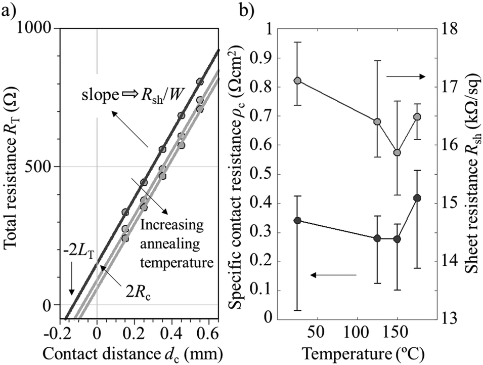 | ||
| Fig. 1 (a) Total resistance (RT) as a function of contact distance (dc) obtained from corresponding I–V curves for the ALD V2O5 film contacted with ITO/Ag. (b) Specific contact resistivity (ρc) and Sheet resistance (Rsh) dependence on annealing temperature extracted from TLM measurements. | ||
Furthermore, the specific contact resistance exhibits a temperature dependence as can be seen in Fig. 1b, where cumulative 10 min annealing steps were made from 100 to 175 °C. The lowest average specific contact resistance value reached in the study corresponds to a 150 °C annealing treatment, reaching a value of 277 mΩ cm2 and a sheet resistance of 15.8 kΩ sq−1. In this case, a minimum and maximum ρc values of 100 and 430 mΩ cm2 were achieved, respectively, with Rsh ranging from 15 to 17 kΩ sq−1.
From a passivation point of view, quasi-steady-state photoconductance (QSS-PC) measurements exhibit effective lifetimes (τeff) of up to 600 μs for as-deposited samples, as can be seen in Fig. 2. After ITO deposition an important drop in surface passivation is observed decreasing lifetime to 140 μs. Damage after sputtering is a well-known phenomenon, damages, fortunately, can sometimes be recovered after a relatively low temperature annealing.38
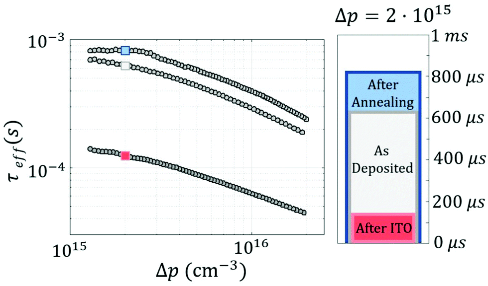 | ||
| Fig. 2 Effective carrier lifetime (τeff) as a function of the excess carrier density (Δp) of c-Si(n) substrate, with asymmetrically passivated front and back surfaces using ALD V2O5 and ALD Al2O3 films, respectively. Bar plot shows the τeff values at Δp = 2 × 1015 cm−3. | ||
It can be seen in Fig. 2, that annealing for 10 min at 150 °C totally recovered the sputtering damage and even enhanced a little more of the surface passivation, reaching τeff values of up to 820 μs. Such high lifetime results in implied open-circuit voltages as high as 690 mV for the finished device structure, and a recombination current density (J0) of 57.7 fA cm−2. This result indicates that evaporated and ALD vanadium films behave differently when exposed to thermal steps. Particularly, ALD deposited V2O5 films exhibited a positive response and a total recovery of sputtering damage.
High-resolution scanning transmission electron microscope (STEM) images evidence the formation of a SiOx interlayer between V2O5 and the crystalline silicon (see Fig. 3a). This spontaneous SiOx growth layer at the silicon surface might explain in part the excellent surface passivation achieved in our films by reducing surface recombination states at the Si interface. Furthermore, X-ray photoelectron spectroscopy (XPS) data (see Fig. 3c) confirm the existence of a silicon oxide by analysing the 2p Si orbital spectrum.
 | ||
| Fig. 3 (a) A high-resolution STEM image of ALD V2O5 film deposited onto bare silicon, and its XPS spectra for the (b) vanadium 2p3/2 orbital and (c) silicon 2p orbital. | ||
This phenomenon also occurs using thermal evaporation as it has been already reported in the literature.13 In addition, in the 2p3/2 vanadium orbital a small presence of a sub-oxidized vanadium state (i.e., V4+) is observed, which could be attributed to deeper gap states. These gap states are correlated to hole extraction through trap-assisted tunnelling.39 Furthermore, traps also contribute to the n-doping of the transition metal oxide layer. This feature is necessary to allow the band to band tunnelling of electrons from the conduction band of the vanadium oxide into the valence band of the crystalline silicon,40,41i.e., the main hole extraction mechanism, which explains the relatively low contact resistance achieved in our samples.
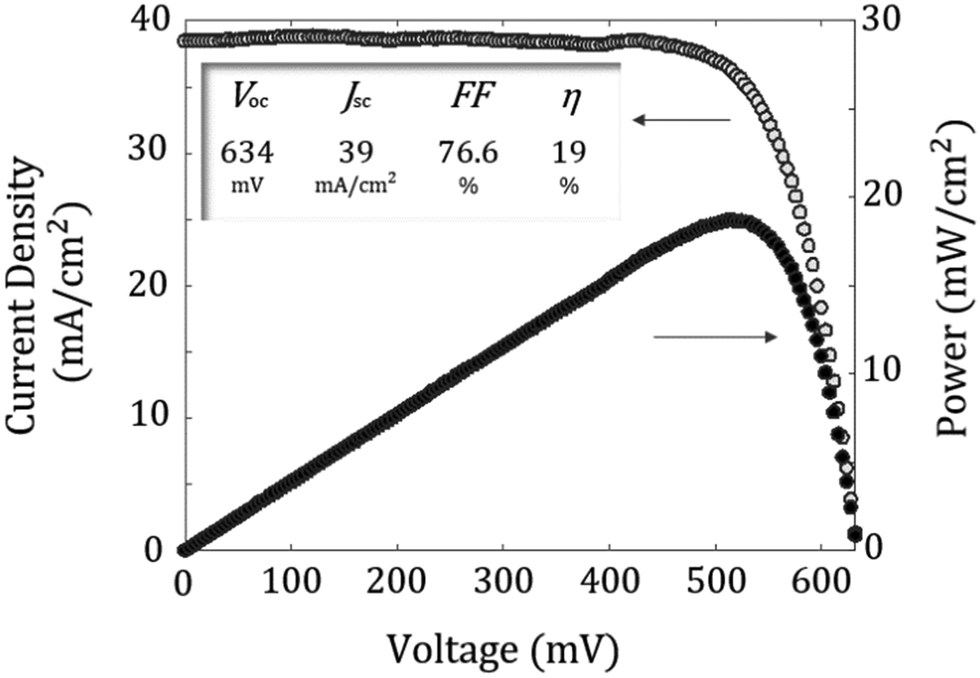
Finally, we fabricated proof-of-concept c-Si solar cells to demonstrate the viability of ALD V2O5 films as a hole-selective contact. The inset of Fig. 4 shows a photograph of finished devices. IV curves under AM 1.5G solar spectrum can be seen in Fig. 7 (1 kW m−2 at 25 °C) with a relatively high mean efficiency of 18.6 ± 0.24%, and an average open-circuit voltage (Voc), short circuit current density (Jsc) and fill factor (FF) of 631 mV, 38.36 mA cm−2 and 75.8%, respectively. The external quantum efficiency (EQE) measurements (Fig. 4) confirmed that excellent front surface passivation is achieved in our cells with Jsc values higher than 38 mA cm−2 in all cases. On the other hand, Voc values of up to 635 mV also confirm that vanadium oxide films provide enough front surface passivation and enhance the obtained Voc in the order of 580/600 mV when compared to similar structures without an amorphous silicon buffer using evaporated TMOs.18,41 This could be due to the high degree of coverage of ALD.
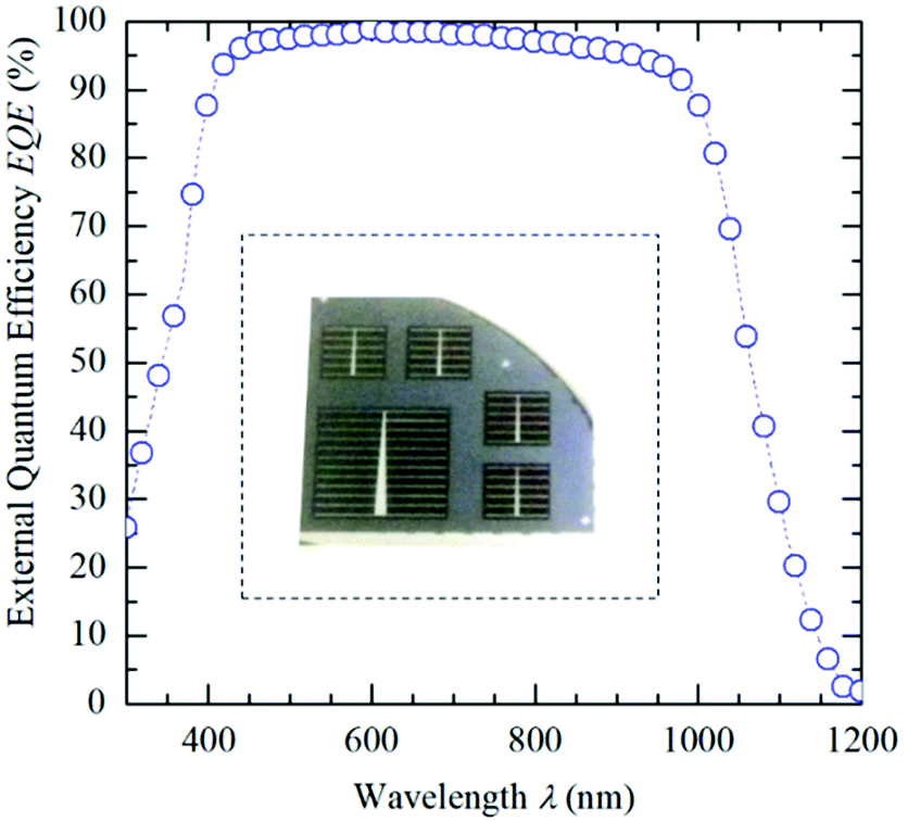 | ||
| Fig. 4 External quantum efficiency (EQE) curve of the best solar cell, in which the EQE beam spot was centered within the metallic fingers (i.e., active device area). Inset: Photography showing solar cells of 1 × 1 and 2 × 2 cm2 configurations. IV curve and power output characteristics of the champion solar cell. | ||
The difference compared to the implied Voc could be attributed to perimeter recombination (notice that in our solar cells there is no surface passivation outside active area), random pyramid surface, which increases the contact area and the non-negligible surface recombination at the rear contact.
From photovoltaic results summarized in Table 1, one can see that the vanadium oxide deposited by ALD can reach significantly high-efficiency solar cells even without the use of an additional interlayer in contrast to other reported works, where a thin interlayer of a-Si:H(i) is required to passivate the surface of c-Si.30
| Area (cm2) | Dark J–V | AM 1.5G J–V | Pseudo J–V | |||||||||
|---|---|---|---|---|---|---|---|---|---|---|---|---|
| J 01 (pA cm−2) | n 1 | J 02 (nA cm−2) | n 2 | R s (Ω cm2) | R shunt (MΩ cm2) | V oc (mV) | J sc (mA cm−2) | FF (%) | η (%) | pFF (%) | pη (%) | |
| 1 | 5.3 | 1.11 | 9.7 | 1.95 | 0.77 | 0.50 | 634 | 39.08 | 76.63 | 19.0 | 81.62 | 20.22 |
| 1 | 7.6 | 1.13 | 22 | 2.25 | 0.75 | 280 | 628 | 38.78 | 77.24 | 18.8 | 82.60 | 20.45 |
| 1 | 8.9 | 1.13 | 28.5 | 2.39 | 0.84 | 30 | 629 | 38.88 | 74.73 | 18.3 | 83.30 | 20.65 |
| 1 | 0.9 | 1.02 | 300 | 2.86 | 0.94 | 5 | 630 | 38.80 | 75.99 | 18.6 | 81.80 | 20.27 |
| 4 | 0.6 | 1.02 | 75 | 2.37 | 1.16 | 80 | 635 | 39.09 | 75.30 | 18.8 | 82.50 | 20.51 |
| Mean ± std | 5.0 ± 3.5 | 1.08 ± 0.06 | 150 ± 100 | 2.36 ± 0.32 | 0.89 ± 0.08 | 79 ± 50 | 631 ± 2.98 | 38.92 ± 0.11 | 75.82 ± 0.98 | 18.6 ± 0.24 | 82.36 ± 0.67 | 20.42 ± 0.17 |
In order to get a deeper insight into the V2O5/c-Si interface configuration, we measured capacitance–voltage curves of the solar cells in reverse bias. With this technique, we can determine the built-in voltage (Vbi) of the junction, which corresponds to the induced band bending at the c-Si in thermal equilibrium.
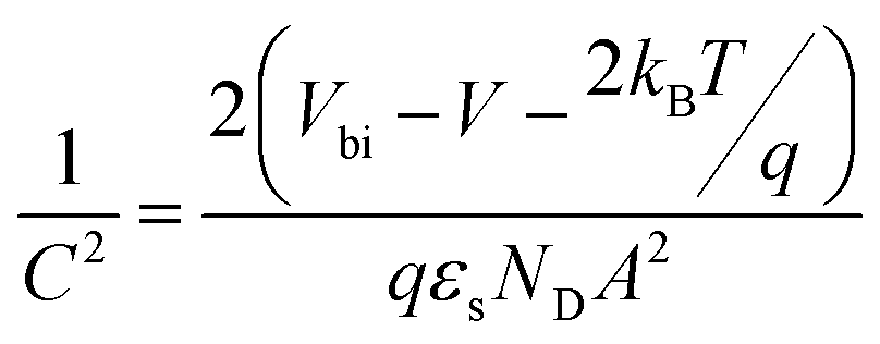
This parameter is extracted from the x-axis crossing point of the C−2vs. voltage curve, known as the Mott–Schottky plot, plotted using the following eqn (1):41
 | (1) |
In Fig. 5, we show the C−2vs. voltage curve measured at 10 kHz for the 4 cm2 solar cell together with the best linear fit with R2 = 0.999925. From the slope of the linear fit, we can obtain the doping density of the substrate (ND = 6.8 × 1015 cm−3, ρ = 0.75 Ω cm), which agrees well with the lower values of the resistivity range provided by the substrate manufacturer. In addition, a Vbi of 683 mV is extracted from the crossing point of the x-axis (V = 632 mV).
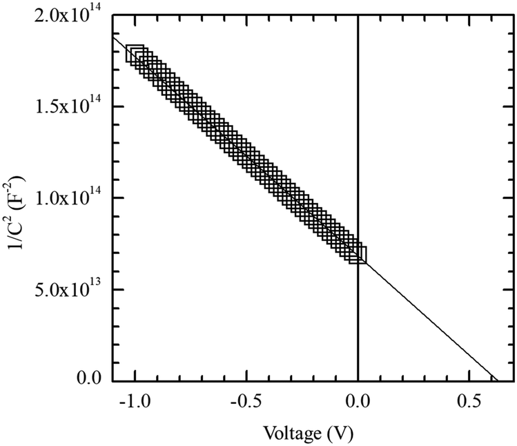 | ||
| Fig. 5 C −2 vs. voltage plot (Mott–Schottky plot) of the 2 × 2 cm2 solar cell. From the x-axis crossing point, a Vbi of 683 mV is deduced indicating an inverted surface. | ||
This band bending induced in c-Si corresponds to a surface with a very strong field-effect passivation. In other words, the surface shows a much higher hole density than electron density (inverted surface) significantly reducing interface recombination. Furthermore, this result confirms the presence of an inverted surface already suggested above by the TLM measurements.
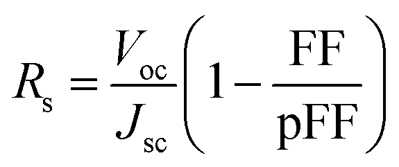
In order to determine the influence of the specific series resistance (Rs) in the solar cell performance, Suns-Voc measurements42 were made to extract the pseudo fill factor (pFF). The Rs parameter can be calculated using eqn (2) provided Voc, Jsc and pFF of the cell.43
 | (2) |
 | (3) |
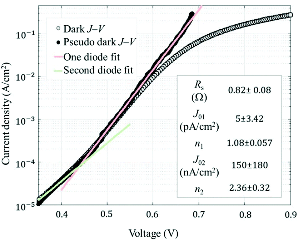 | ||
| Fig. 6 Dark J–V and pseudo dark J–V curves for the best solar cell. The pseudo J–V characteristic, free of series resistance effects, is determined from Suns-Voc measurements. The fitting parameters are shown in the inset. | ||
 | ||
| Fig. 7 Light J–V and power output curves for the best solar cell. Photovoltaic parameters are shown in the inset. | ||
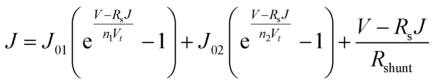
By comparing pFF and FF values, we can conclude that the main mechanism that limits fill factor and efficiency is the series resistance, which is in the 0.75–1.16 Ω cm2 range. In order to elucidate the contribution of contact resistance of the V2O5-based HTL in our finished solar cells, we can apply eqn (4).45
 | (4) |
Using eqn (4), we can extract ρc considering the average Rs value of 0.89 Ω cm2, reaching 0.33 Ω cm2 in our V2O5/ITO selective contacts deposited on the random pyramid textured surface. Curiously, this value is similar to that achieved in the TLM test samples on the polished surface despite of the increase in the contacted area due to the texturized surface. Notice that the contribution of ρc in the total resistance is below 37%, suggesting that there is still room to improve the fill factor, i.e., using a metallization with higher thickness of Ag and/or reducing the sheet resistance of the ITO layer.
Experimental
The test sample and solar cell devices were fabricated using high-quality 〈100〉 float zone n-type c-Si (c-Si) wafers of 4” with resistivity and thickness of 1.5 ± 1 Ω cm and 280 ± 20 μm, respectively. The specific contact resistance (ρc) of ALD V2O5 selective contact was determined using transfer length measurements (TLM) summarized for contact resistivity as follows in eqn (5):46,47 | (5) |
TLM samples (see Fig. 8a) were prepared on polished c-Si(n) wafers, which had been previously cleaned following standard RCA cleaning procedure,48 plus a diluted HF (1%) dip for 1 minute obtaining, as a result, hydrophobic silicon surfaces. Next, samples were introduced into the ALD system (Savannah S200, Cambridge Nanotech) and they were covered with a 4 nm thick V2O5 layer. Tetrakis(ethylmethylamino)-vanadium(IV) (i.e., C12H32N4V) and deionized water (DI-H2O) were used as the vanadium precursor and oxidant species, respectively. The deposition process was performed at 125 °C and the vanadium precursor was heated at 58 °C, resulting in an estimated growth rate of 0.4 Å per cycle. Then, a 70 nm thick indium-tin-oxide (ITO) film was deposited using RF magnetron sputtering at 50 W, using a shadow-mask technique to pattern TLM contacts. Finally, without removing the shadow mask, a 200 nm thick silver layer was thermally evaporated over the ITO film. The dependence of contact resistance on thermal treatments was studied using 10 min hot plate annealing under nitrogen (N2) rich ambient.
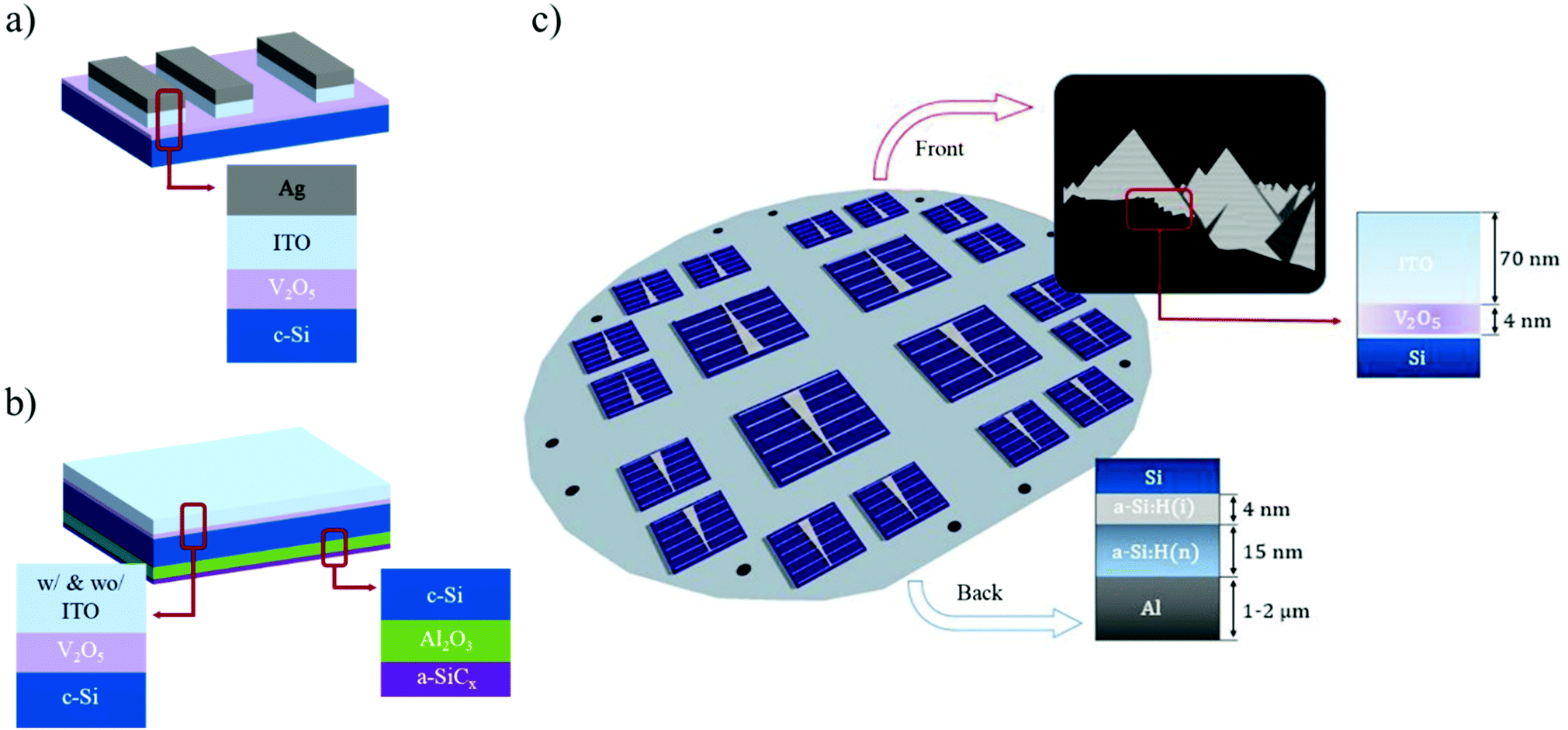 | ||
| Fig. 8 Schematic diagram of: (a) TLM film structure. (b) QSSPC film structure (c) solar cell film structure. | ||
Surface passivation properties of ALD V2O5 films were obtained by the effective lifetime (τeff) measurements, using the quasi-steady-state photoconductance (QSS-PC) technique49 with a WCT-120 instrument (Sinton Consulting). Asymmetrical test samples were prepared for this purpose (see Fig. 8b), with a back-surface excellently passivated with an alumina film (i.e., surface recombination velocity close to zero) and a front surface covered with the corresponding film under study, following the next steps: first, after RCA cleaning, a 50 nm thick ALD alumina film was deposited on both sides at a temperature of 200 °C. Trimethylaluminum (TMA) and DI-H2O were used as the aluminum precursor and oxidant species, respectively. A subsequent annealing treatment, 10 min in forming gas (FG) ambient at 400 °C, was made to activate surface passivation provided by alumina films.50 In order to protect the alumina film in the subsequent process etching stages, a 35 nm thick silicon carbide layer (a-SiCx) film was deposited over alumina on the backside using the plasma-enhanced chemical vapor deposition (PECVD) process (13.56 MHz, from Elettrorava S.p.A). This stage was made at 300 °C using methane (CH4) and silane (SiH4) as precursor gases in the PECVD reactor. Finally, after an HF (1%) dip to remove the front-side alumina film (i.e., obtaining a bare hydrophobic c-Si surface) a 4 nm thick V2O5 film was deposited at 125 °C, using the same conditions described before for the TLM test samples. The passivation properties after ITO deposition were also studied, in which a 70 nm thick ITO layer was deposited over V2O5 using the same sputtering conditions for TLM test samples. Healing of any eventual damage by the sputtering process was performed with a final annealing treatment at 150 °C for 10 min on a hot plate in N2 ambient.
The surface composition of V2O5 films was determined using X-ray photoelectron spectroscopy (XPS) (SPECS, hemispherical energy analyzer PHOIBOS 150). The scan was performed using a non-monochromatic Al-Kα X-ray excitation source at 1486.6 eV and 3 × 10⁻⁹ mbar.
Current density vs. voltage (J–V) electrical characteristics of the complete devices were measured under a four-probe configuration using a Keithley 2601B Source Meter.
Solar cells of 1 × 1 and 2 × 2 cm2 active area were fabricated to demonstrate the viability of V2O5 films as a hole-selective contact. The device structure is depicted in Fig. 8c. The fabrication process started with the texturization of the front side c-Si(n) wafer with random pyramids by alkaline etching using tetramethylammonium hydroxide (TMAH) alkaline-based solution. Then, the substrate was cleaned by a standard RCA procedure and HF (1%) dip for 1 min, followed by the deposition of an intrinsic and a phosphorus-doped amorphous silicon stack [a-Si:H(i)/a-Si:H(n)] with thicknesses of 4 and 15 nm, respectively. The stack was deposited by the same foregoing PECVD equipment used for the test samples at a temperature of 300 °C. Next, just after another RCA cleaning process, the ALD V2O5 film (4 nm) was deposited on the front surface and immediately introduced into the sputtering chamber to deposit a 70 nm thick ITO layer at 50 W. Next, front active solar cell areas were defined using standard photolithography and wet etching (HF (2%) dip, 2 min). After that, a fully back-contact metallization was performed using a thermally evaporated Al film (1 μm) over the a-Si:H(i)/a-Si:H(n) stack. Finally, the front-contact silver grid (50 μm wide fingers) was thermally evaporated using a shadow-mask, resulting in a metal fraction area of around 4%. Final annealing in forming gas ambient at 150 °C was made to recover sputtering damage. Photovoltaic parameters and current–voltage curves were measured under standard test conditions AM 1.5G solar spectrum (1 kW m−2 at 25 °C) using an ORIEL 94021A (Newport) solar simulator, the light irradiance of which was properly calibrated using a pyranometer. External quantum efficiencies (EQE) curves were obtained using a commercial instrument (QEX10, PV measurements) with a white light bias of 0.2 Suns and a beam spot placed directly onto the ITO and out of the metallic fingers patterned on the front surface (i.e., the active device area).
Conclusions
In this work, we studied the vanadium oxide thin films deposited by ALD and studied their application as a hole transport layer in crystalline silicon solar cells as a transparent electrode without a PECVD buffer passivation layer.TLM measurements of V2O5 (ALD)/ITO/Ag stacks on c-Si(n) confirm low contact resistances, reaching values as low as 40 mΩ cm2 with an average value of 0.4 Ω cm2. Furthermore, the observed sheet resistance of TMO is in the order of 15–20 kΩ sq−1 correlating to the presence of a p+ inversion layer beneath the film. Capacitance measurements on the stack also evidenced the presence of an inversion layer with a built-in voltage value of 683 mV. This inverted layer also provides both low contact resistance and good surface passivation with effective minority carrier lifetimes up to 800 μs after thermal treatment.
Finally, we tested ALD-deposited vanadium oxide as the HTL in c-Si solar cells. The fabricated cells measured under standard AM 1.5G solar spectrum (1 kW m−2, T = 25 °C) exhibited efficiencies of 18.6% on average, with mean values of Voc, Jsc and FF of 631 mV, 38.9 mA cm−2 and 75.8%, respectively. The low scattering between photovoltaic parameter values points out a remarkable reproducibility between devices, indicating a high layer conformal deposition over a four-inch wafer. The top solar cell achieved significant performance parameters with an efficiency of up to ∼19% without passivation from amorphous silicon. The main limiting factor in the final photovoltaic efficiency is the series resistance achieved by our finished device design corresponding to 0.89 Ω cm2 on average. However, the contribution of the V2O5-based front contact is estimated to be only 37% of the total series resistance. Therefore, technological improvements in cell fabrication, such as better electrical quality of the ITO layer (Rsh < 120 Ω sq−1) and/or a thicker silver grid could improve current efficiencies closer to the calculated pseudoefficiencies (>20%) and closer to those reported by Yang et al.,34 21.6%, with an enhanced current provided by the use of wide bandgap materials in the front contact.
With the current range of efficiencies obtained in this study, we conclude that ALD is a suitable deposition technique for transition metal oxides as it is useful, particularly, for vanadium oxide on crystalline silicon for photovoltaic applications.
Conflicts of interest
The authors declare that there are no conflicts of interest in regard of this manuscript.Acknowledgements
This work was supported by the Spanish Government through Projects ENE2016-78933-C4-1-R, ENE2017-87671-C3-2-R, PID2020-116719RB-C41 and TEC2017-82305-R. The H2020 European Research Council Grant (SENSATE, H2020-ERC-CoG-2019-866018) is gratefully acknowledged. Authors from IREC acknowledge the European Regional Development Funds (ERDF, FEDER Programa Competitivitat de Catalunya 2007–2013) and CERCA Programme/Generalitat de Catalunya that belongs to the SEMS (Solar Energy Materials and Systems) Consolidated Research Group of the “Generalitat de Catalunya” (Ref. 2017 SGR 862). Additionally, this was also supported by Basic Science Research Program (NRF-2014R1A6A1030419) through the National Research Foundation of Korea (NRF) funded by the Ministry of Education.Notes and references
- F. Ise, Photovoltaics Report. http://www.ise.fraunhofer.de.
- A. Bhambhani, “World's Lowest Solar Bid Disqualified | TaiyangNews,” Taiyang News, 2018. [Online]. Available: http://taiyangnews.info/markets/worlds-lowest-solar-bid-disqualified/. [Accessed: 16-Jan-2020].
- V. Shah and J. Booream-Phelps, Crossing the Chasm. ( 2015) Search PubMed.
- U.S. Energy Information Administration. Levelized Cost and Levelized Avoided Cost of New Generation Resources in the Annual Energy Outlook 2019. (2019).
- C. Battaglia, et al., Silicon heterojunction solar cell with passivated hole selective MoO x contact, Appl. Phys. Lett., 2014, 104(11), 113902 CrossRef.
- K. Yoshikawa, et al., Silicon heterojunction solar cell with interdigitated back contacts for a photoconversion efficiency over 26%, Nat. Energy, 2017, 2, 17032 CrossRef CAS.
- K. Yoshikawa, et al., Exceeding conversion efficiency of 26% by heterojunction interdigitated back contact solar cell with thin film Si technology, Solar Energy Mater. Solar Cells, 2017, 173, 37–42 CrossRef CAS.
- SunPower (USA) November, 2015. Judged from the “Solar cell efficiency tables(version 47)” [Prog. Photovolt: Res. Appl. 2016; 24:3-11].
- Y. Chen, et al., Mass production of industrial tunnel oxide passivated contacts (i-TOPCon) silicon solar cells with average efficiency over 23% and modules over 345 W, Prog. Photovoltaics, 2019, 27, 827–834 CAS.
- F. Feldmann, M. Bivour, C. Reichel, M. Hermle and S. W. Glunz, Passivated rear contacts for high-efficiency n-type Si solar cells providing high interface passivation quality and excellent transport characteristics, Solar Energy Mater. Solar Cells, 2014, 120, 270–274 CrossRef CAS.
- J. Bullock, et al., Lithium Fluoride Based Electron Contacts for High Efficiency n-Type Crystalline Silicon Solar Cells, Adv. Energy Mater., 2016, 6, 1600241 CrossRef.
- Y. Wan, et al., Magnesium Fluoride Electron-Selective Contacts for Crystalline Silicon Solar Cells, ACS Appl. Mater. Interfaces, 2016, 8, 14671–14677 CrossRef CAS PubMed.
- L. G. Gerling, et al., Transition metal oxides as hole-selective contacts in silicon heterojunctions solar cells, Solar Energy Mater. Solar Cells, 2016, 145, 109–115 CrossRef CAS.
- G. Masmitjà, et al., Interdigitated back-contacted crystalline silicon solar cells with low-temperature dopant-free selective contacts, J. Mater. Chem. A, 2018, 6, 3977–3985 RSC.
- X. Yang, P. Zheng, Q. Bi and K. Weber, Silicon heterojunction solar cells with electron selective TiOx contact, Solar Energy Mater. Solar Cells, 2016, 150, 32–38 CrossRef CAS.
- X. Yang, P. Zheng, Q. Bi and K. Weber, Silicon heterojunction solar cells with electron selective TiOx contact, Solar Energy Mater. Solar Cells, 2016, 150, 32–38 CrossRef CAS.
- X. Yang, et al., High-Performance TiO2-Based Electron-Selective Contacts for Crystalline Silicon Solar Cells, Adv. Mater., 2016, 28, 5891–5897 CrossRef CAS PubMed.
- C. Battaglia, et al., Hole selective MoOx contact for silicon solar cells, Nano Lett., 2014, 14, 967–971 CrossRef CAS.
- C. Battaglia, et al., Hole selective MoOx contact for silicon solar cells, Nano Lett., 2014, 14, 967–971 CrossRef CAS PubMed.
- P. Würfel and U. Würfel, Physics of Solar Cells: From Principles to New Concepts, Wiley-VCH Verlag GmbH & Co., 2009 Search PubMed.
- F. Feldmann, et al., High and Low Work Function Materials for Passivated Contacts. Energy Proc., Elsevier Ltd, 2015, vol. 77, pp. 263–270 Search PubMed.
- M. Bivour, et al., Principles of Carrier-Selective Contacts Based on Induced Junctions.
- C. Battaglia, et al., Hole Selective MoOx Contact for Silicon Solar Cells, Nano Lett., 2014, 14, 967–971 CrossRef CAS.
- G. Masmitjà, et al., V2Ox-based hole-selective contacts for c-Si interdigitated back-contacted solar cells, J. Mater. Chem. A, 2017, 5, 9182–9189 RSC.
- M. Bivour, J. Temmler, H. Steinkemper and M. Hermle, Molybdenum and tungsten oxide: High work function wide band gap contact materials for hole selective contacts of silicon solar cells, Solar Energy Mater. Solar Cells, 2015, 142, 34–41 CrossRef CAS.
- L. G. Gerling, et al., Transition metal oxides as hole-selective contacts in silicon heterojunctions solar cells, Solar Energy Mater. Solar Cells, 2016, 145, 109–115 CrossRef CAS.
- G. Masmitjà, et al., Interdigitated back-contacted crystalline silicon solar cells with lowerature dopant-free selective contacts, J. Mater. Chem. A, 2018, 6, 3977–3985 RSC.
- J. Dréon, et al., 23.5%-efficient silicon heterojunction silicon solar cell using molybdenum oxide as hole-selective contact, Nano Energy, 2020, 70, 104495 CrossRef.
- L. G. Gerling, C. Voz, R. Alcubilla and J. Puigdollers, Origin of passivation in hole-selective transition metal oxides for crystalline silicon heterojunction solar cells, J. Mater. Res., 2017, 32, 260–268 CrossRef CAS.
- O. Almora, et al., Superior performance of V2O5 as hole selective contact over other transition metal oxides in silicon heterojunction solar cells, Solar Energy Mater. Solar Cells, 2017, 168, 221–226 CrossRef CAS.
- L. G. Gerling, C. Voz, R. Alcubilla and J. Puigdollers, Origin of passivation in hole-selective transition metal oxides for crystalline silicon heterojunction solar cells, J. Mater. Res., 2017, 32, 260–268 CrossRef CAS.
- P. C. Stair, et al., Performance and characterization of ALD vanadium oxide catalytic nanoliths, ECS Trans., 2009, 25, 49–55 CrossRef CAS.
- J. C. Badot, A. Mantoux, N. Baffier, O. Dubrunfaut and D. Lincot, Electrical properties of V2O5 thin films obtained by atomic layer deposition (ALD), J. Mater. Chem., 2004, 14, 3411–3415 RSC.
- X. Yang, et al., Atomic Layer Deposition of Vanadium Oxide as Hole-Selective Contact for Crystalline Silicon Solar Cells, Adv. Electron. Mater., 2020, 6, 2000467 CrossRef CAS.
- B. Macco, M. F. J. Vos, N. F. W. Thissen, A. A. Bol and W. M. M. Kessels, Low-temperature atomic layer deposition of MoOx for silicon heterojunction solar cells, Phys. Status Solidi RRL, 2015, 9, 393–396 CrossRef CAS.
- G. Gregory, et al., Spatial Atomic Layer Deposition of Molybdenum Oxide for Industrial Solar Cells, Adv. Mater. Interfaces, 2020, 7(22), 2000895 CrossRef CAS.
- L. Gerling, S. Mahato, C. Voz, R. Alcubilla and J. Puigdollers, Characterization of Transition Metal Oxide/Silicon Heterojunctions for Solar Cell Applications, Appl. Sci., 2015, 5, 695–705 CrossRef CAS.
- S. Grover, Effect of Transmission Line Measurement (TLM) Geometry on Effect of Transmission Line Measurement (TLM) Geometry on Specific Contact Resistivity Determination Specific Contact Resistivity Determination. https://scholarworks.rit.edu/theses (2016).
- C. Messmer, M. Bivour, J. Schön and M. Hermle, Efficient hole extraction for metal oxide based silicon heterojunction solar cells: A simulation study. AIP Conference Proceedings, vol. 1999, p. 040013, American Institute of Physics Inc., 2018 Search PubMed.
- C. Messmer, M. Bivour, J. Schon, S. W. Glunz and M. Hermle, Numerical Simulation of Silicon Heterojunction Solar Cells Featuring Metal Oxides as Carrier-Selective Contacts, IEEE J. Photovoltaics, 2018, 8, 456–464 Search PubMed.
- L. G. Gerling, S. Mahato, C. Voz, R. Alcubilla and J. Puigdollers, Characterization of transition metal oxide/silicon heterojunctions for solar cell applications, Appl. Sci., 2015, 5, 695–705 CrossRef CAS.
- R. A. Sinton and A. Cuevas A quasi-stead-state open-circuit voltage method for solar cell characterization. in 16th European Photovoltaic Solar Energy Conference 1–5 (2000).
- D. Pysch, A. Mette and S. W. Glunz, A review and comparison of different methods to determine the series resistance of solar cells, Solar Energy Mater. Solar Cells, 2007, 91, 1698–1706 CrossRef CAS.
- A. Hovinen, Fitting of the solar cell IV-curve to the two diode model, Phys. Scripta, 1994, 175, 2007 Search PubMed.
- A. B. Morales Vilches, Desarrollo de tecnologías de baja temperatura para la fabricación de células solares de heterounión de silicio, TDX (Tesis Doctorals en Xarxa), Universitat Politàcnica de Catalunya, 2015.
- H. H. Berger, Contact Resistance and Contact Resistivity, J. Electrochem. Soc., 1972, 119, 507–514 CrossRef CAS.
- S. Grover, Effect of Transmission Line Measurement (TLM) Geometry on Specific Contact Resistivity Determination. Theses, 2016 Search PubMed.
- W. Kern, The Evolution of Silicon Wafer Cleaning Technology, J. Electrochem. Soc., 1990, 137, 1887 CrossRef CAS.
- R. A. Sinton, A. Cuevas and M. Stuckings, Quasi-steady-state photoconductance, a new method for solar cell material and device characterization. in Conference Record of the Twenty Fifth IEEE Photovoltaic Specialists Conference – 1996, pp. 457–460 (IEEE, 1996), DOI: 10.1109/PVSC.1996.564042.
- B. Hoex, J. Schmidt, P. Pohl, M. C. M. van de Sanden and W. M. M. Kessels, Silicon surface passivation by atomic layer deposited Al2O3, J. Appl. Phys., 2008, 104, 044903 CrossRef.
Footnote |
| † Electronic supplementary information (ESI) available. See DOI: 10.1039/d1ma00812a |
| This journal is © The Royal Society of Chemistry 2022 |