DOI:
10.1039/D1MA00806D
(Paper)
Mater. Adv., 2022,
3, 624-631
van der Waals graphene/MoS2 heterostructures: tuning the electronic properties and Schottky barrier by applying a biaxial strain
Received
4th September 2021
, Accepted 10th November 2021
First published on 13th November 2021
Abstract
First principles calculations are performed to study the effects of the interlayer distance and biaxial strain on the electronic properties and contact properties of graphene/MoS2 heterostructures. The interlayer interaction is weakened and the charge transfer from the graphene layer to the MoS2 layer is reduced with increasing interlayer distance in graphene/MoS2 heterostructures, resulting in a shift of the Fermi level to a high energy state. The n-type Schottky barrier is formed with ΦSB,N values of 0.647 eV, 0.568 eV, 0.509 eV, and 0.418 eV when the interlayer distances are 3.209 Å, 3.346 Å, 3.482 Å, and 3.755 Å, respectively. The interlayer distance and charge density difference change slightly, but the electronic structure of the graphene/MoS2 heterostructure changes obviously by applying the biaxial strain. For the biaxial strain from −4% to +6%, the ΦSB,P gradually increases for the graphene/MoS2 heterostructure, while the ΦSB,N increases initially and then decreases. Moreover, the ΦSB,N is only 0.080 eV under a biaxial strain of +6%, indicating that the Ohmic contact is nearly formed. The results demonstrate the significant effects of a biaxial strain on the physical properties of 2D heterostructures.
1. Introduction
Since the discovery of graphene in 2004, its unique physics and novel applications have triggered extensive research.1–3 Although the extremely high electrical conductivity makes graphene a potential candidate material to replace silicon-based electronic devices, Klein tunneling causes the electrical transport of Dirac fermions insensitive to the electrostatic potentials, which leads to a low current on/off ratio of graphene-based field effect transistors.4–6 In order to realize graphene electronics, it is very important to manipulate the electronic properties without impairing its high mobility.
An important milestone is the creation of heterostructures based on graphene and other two dimensional (2D) materials, which can be assembled into three dimensional stacks with atomic layer precision.7–9 Such layered structures have already demonstrated a range of fascinating physical phenomena. Wang et al. found that for the MoS2/ZnO heterostructure the strong optical absorption in the visible region indicates that it has potential for application in photovoltaic and photocatalytic devices.10 The type-II band alignment occurs at MX2/graphene-like zinc oxide interfaces, together with the large built-in electric field across the interface.11,12 Due to the inherent weak absorption characteristics and small built-in potential of 2D material photodetectors, their external quantum efficiency is severely limited to the range of ∼0.1–1%.13,14 Duan et al.15 modulated the amplitude and polarity of photocurrent in the gated vertical garphene/MoS2 heterostructures via the electric field of an external gate. The maximum external quantum efficiency and internal quantum efficiency are estimated to be 55% and 85%, respectively. Moreover, graphene/MoS2 heterostructures display highly sensitive photodetection and gate tunable persistent photoconductivity.16 The responsivity of the heterostructures is nearly 1 × 10¹⁰ A W−1 at 130 K and 5 × 10⁸ A W−1 at room temperature. The heterostructures could also function as a rewritable optoelectronic switch or a memory device when irradiated by the time-dependent photoillumination, where the persistent state shows almost no relaxation or decay within experimental timescales, indicating near-perfect charge retention.
Compared with metal/2D material heterostructures, the use of 2D materials to construct van der Waals vertically stacked heterostructures is one of the effective and feasible ways to reduce the effect of Fermi level pinning. Graphene has potential applications in 2D transistors due to its excellent electrical conductivity, for example, in high-performance devices and circuits based on graphene/MoS2 heterostructures, where MoS2 is used as the transistor channel and graphene as contact electrodes.17 As we all know, there are two mechanisms by which charge can be injected into a semiconductor: thermionic emission over the semiconductor and field emission across the semiconductor. The thermionic emission–diffusion theory describes the current–voltage characteristics of a metal/semiconductor heterostructure as a function of the Schottky barrier height. Carrier recombination can also be a current-limiting process if an inversion layer is present near the contact. Contrary to the bulk case, where the diffusion region extends both laterally and vertically into the semiconductor, in a metal/2D semiconductor heterostructure with no hybridization, the position of the bands vary only laterally, so that charge carriers injected far from the contact edge first encounter the flat-band region before the diffusion region. In this case, the relative contributions from thermionic emission and tunnelling become difficult to predict. On the basis of a thermionic field emission model, the barrier height at the graphene/MoS2 heterostructure was determined to be 0.23 eV and the tunability of graphene work function with electrostatic doping significantly improves the Ohmic contact.18 Wei-Qing Huang et al.19 found that the transformation from an n-type Schottky barrier to a p-type Schottky barrier can be realized in MoSxSe(2−x)/graphene heterostructures when the Se concentration is greater than 25%. Interestingly, the Schottky type, Schottky barrier height, and contact types at the interface can be tuned by an external electric field.19,20 On the other hand, because of their excellent Young's modulus, graphene and MoS2 hold promise for applications in flexible electronic devices. A highly flexible transistor was developed based on an exfoliated MoS2 channel and CVD-grown graphene source/drain electrodes, and a low Schottky barrier (∼22 meV) forms.21–24 The graphene/MoS2 heterostructures exhibit a Young's modulus that is about three times that of monolayer MoS2, while correspondingly exhibiting a yield strain that is about 30–40% smaller than that of monolayer MoS2 due to lateral buckling of the outer graphene layers.25 Zhou et al.26–28 found that the tensile strain can enhance the optical absorption in the visible range and increase the solar energy conversion efficiency for 2D heterostructures.26–28 Moreover, with an appropriate compressive strain of 2% and 3%, the WTe2-As heterostructures show transition from the type-I to type-II band alignment, which could slow down electron–hole pair recombination.29 However, to date the effects of the strain on the structural and electronic properties of the graphene/MoS2 heterostructures have not yet been studied systematically.
Herein, first principles calculations are done to systematically study the effects of the interlayer distance and biaxial strain on the electronic structure and contract properties of the graphene/MoS2 heterostructures. Although the charge transfers from the graphene layer to MoS2 layer, the electronic band structure seems to be a simple sum of those of each constituent when graphene stacks on top of the MoS2 layer. And the contact properties are insensitive to the interlayer distance. While the biaxial strain engineering is a valuable method to modulate the electronic structure and contact properties of the graphene/MoS2 heterostructures.
2. Computational method
All calculations are performed using VASP based on density functional theory.30,31 The electron–ion core interaction and the exchange–correlation interaction are described by the projector augmented wave potentials32 and the Perdew–Burke–Ernzerhof formulation of the generalized gradient approximation,33 respectively. The DFT–D2 approach in the Grimme scheme is adopted to include the contribution from the vdW interaction between layers.34 The cutoff energy for the plane-waves is chosen to be 400 eV. According to the Monkhorst–Pack scheme, Brillouin zone integration is performed by using an 11 × 11 × 1 k-mesh and Gaussian smearing broadening of 0.2 eV is adopted. In order to relax the ions to the ground states with an energy convergence of 1.0 × 10⁻⁵ eV and a force convergence of 0.02 eV Å−1 on each ion, a conjugate-gradient algorithm is employed. Visualizations of supercells and structures are done with the software VESTA.35
The thermodynamic stability of graphene/MoS2 heterostructures is evaluated by calculating the binding energy (Eb) as shown in the following equation:
| | | Eb = [Egraphene/MoS2 − (Egraphene + EMoS2)]/NC, | (1) |
where
Eb, and
Egraphene/MoS2,
Egraphene, and
EMoS2 are the binding energy, and the total energy of the graphene/MoS
2 heterostructure, graphene and MoS
2 monolayers, respectively.
NC is the number of carbon atoms in the supercell. When
Eb is negative, the system is stable. And the larger the absolute value of the
Eb value, the stronger the heterostructure binding. To gain further insight into the bonding nature and interlayer interaction, the plane-averaged charge density difference (Δ
ρ) was calculated as shown in the following equation:
| | | Δρ = ρgraphene/MoS2−ρgraphene−ρMoS2, | (2) |
in which
ρgraphene/MoS2,
ρgraphene, and
ρMoS2 are the plane-averaged charge densities of the graphene/MoS
2 heterostructure, graphene and MoS
2 monolayers, respectively.
3. Results and discussion
3.1 Graphene/MoS2 heterostructure
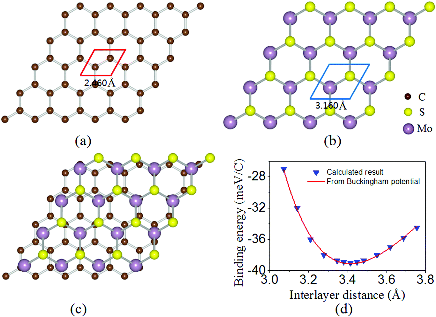
The optimized lattice constants of monolayer graphene and MoS2 are 2.460 Å and 3.160 Å [as shown in Fig. 1(a and b)]. To limit the lattice mismatch between graphene and MoS2 in our calculations, the simulation cell is built from a 5 × 5 graphene supercell and a 4 × 4 MoS2 supercell [Fig. 1(c)]. The lattice constant of the graphene/MoS2 heterostructure is fixed as that of MoS2 and changes the lattice constant of graphene to adjust to those of MoS2, where graphene is under a biaxial tensile strain of 2.69% and no significant changes in the electronic properties in the heterostructure. Additionally, previous work has indicated that the structural and electronic properties of the graphene/MoS2 heterostructure are independent of the atomic configuration.36 Thus, the other atomic configuration of graphene adsorbed on MoS2 is not taken into account.
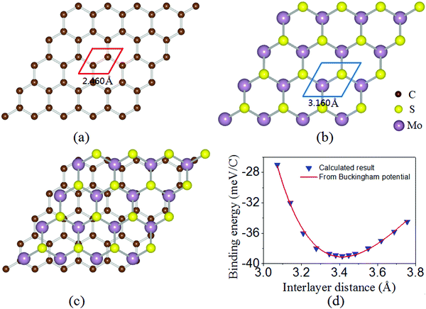 |
| | Fig. 1 Optimized geometries for the top view of (a) graphene and (b) MoS2 monolayers, and (c) graphene/MoS2 heterostructure. (d) Binding energy of graphene per C as a function of the interlayer distance between graphene and the topmost S atom of MoS2 for the graphene/MoS2 heterostructure. | |
The equilibrium structure is yielded by applying the two-step optimization on the designed lattice. For step one, the interlayer distance is changed and the binding energy was calculated, and also the results were fitted into the well-known Buckingham potential equation:
| |  | (3) |
in which
A,
B, and
C are fitting parameters of −7.492 eV, 1.158 Å, and −136.063 eV Å, respectively.
6d and
Eb are the interlayer distance and the binding energy, respectively. The binding energy as a function of the interlayer distance and fitting curve is shown in
Fig. 1(d). The predicted equilibrium interlayer distance read from the fitting curve is about 3.410 Å. For step two, a structure with an interlayer distance of 3.410 Å is constructed and placed into a full relaxation to yield the final equilibrium structure. After optimization, the interlayer distance between the monolayer MoS
2 and graphene is 3.414 Å, with a binding energy of −39 meV per C atom, which is of the same order of magnitude as that of other heterostructures such as MoS
2/graphene,
37 black phosphorene/graphene,
38–41 and arsenene/graphene.
42,43
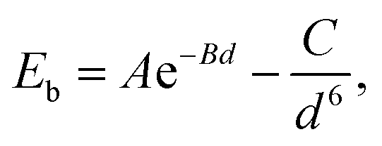
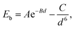
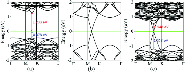
Next, the calculated electronic band structure of the graphene/MoS2 heterostructure is displayed in Fig. 2(c). For comparison, the electronic band structures of pristine graphene and isolated MoS2 monolayers are also shown in Fig. 2(a and b). For the graphene/MoS2 heterostructure, the electronic band structure seems to be a simple sum of those of each constituent. The linear dispersion bands of graphene appear in the large energy gap of MoS2, and the character of the electronic band structure of pristine graphene seems to be preserved, indicating the weak interaction between graphene and MoS2. In Fig. 3(a), the band alignment is schematically demonstrated to show the formation of interlayer excitons. In particular, excited electrons from graphene migrate to MoS2, while holes go oppositely owing to the difference between their Fermi levels, and the electrons and holes can be held together by strong Coulomb interactions. The charge difference of graphene/MoS2 heterostructure is calculated. As expected, the charge redistribution mainly occurs at the interface between the layers, with an accumulation of electrons on the MoS2 layer and a depletion of charges on the graphene layer [Fig. 3(b and c)]. Furthermore, it can be found that the potential of graphene (8.881 eV) in the graphene/MoS2 heterostructure is deepened as shown in Fig. 3(d). The large potential drop of the grapene/MoS2 heterostructure indicates a strong electronic field across the interface, which may affect the kinetics of photo-generated carriers.44
 |
| | Fig. 2 Band structures of (a) graphene and (b) MoS2 monolayers, as well as (c) graphene/MoS2 heterostructure. The Fermi level is indicated by the green line. | |
 |
| | Fig. 3 (a) Schematic representation of the band alignment for graphene and MoS2 monolayers, as well as the graphene/MoS2 heterostructure. (b) Plane averaged charge density differences, (c) three dimensional isosurface of the charge density difference, and (d) plane averaged effective potential of the graphene/MoS2 heterostructure. The red and green areas represent electron accumulation and depletion, respectively, and the isosurface value is 2 × 10⁻⁴ e Å−3. | |
3.2 Effects of interlayer distance on the graphene/MoS2 heterostructure
Charging the interlayer distance is an effective approach to tune the electronic properties of the van der Waals heterostructure. Moreover, the interlayer distance in the van der Waals heterostructure can be easily controlled in experiments by vacuum thermal annealing, nanomechanical pressure, or a diamond anvil cell.45–47 Thus, it is necessary to consider the influence of the interlayer distance on the electronic properties of the graphene/MoS2 heterostructure.
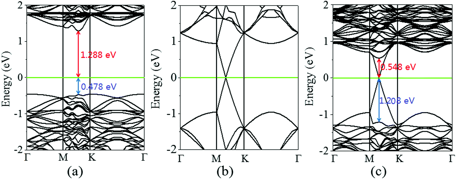
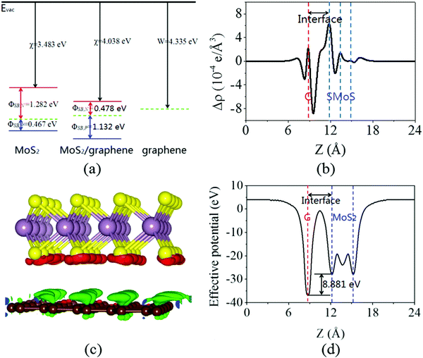
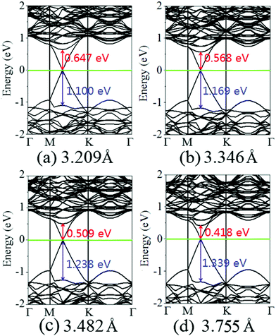
Fig. 4 displays the charge density difference of the graphene/MoS2 heterostructure as the interlayer distance changes. From Fig. 4(a), one can observe that the fluctuation of the differential charge density curve increases when the interlayer distance is reduced from 3.755 Å to 3.209 Å, indicating the more charge transfers from the graphene layer to the MoS2 layer. Moreover, according to Mulliken charge analysis, 0.120 e, 0.107 e, 0.088 e, and 0.062 e transfer from the graphene layer to MoS2 layer when the interlayer distances are 3.209 Å, 3.346 Å, 3.482 Å, and 3.755 Å, respectively. The Fermi level of the graphene shifts downwards due to its charge transfers to the MoS2 layer, while the electronic band structures of pristine graphene and MoS2 monolayers are preserved. The band gaps of the MoS2 layer in heterostructures are 1.747 eV, 1.737 eV, 1.747 eV, and 1.757 eV when the interlayer distances are 3.209 Å, 3.346 Å, 3.482 Å, and 3.755 Å, respectively (Fig. 5). All these results indicate that the interlayer distance is effective to control the charge transfer, while limited to regulate the electronic structure (Table 1).
 |
| | Fig. 4 (a) Plane averaged charge density difference and (b) three dimensional isosurface of the charge density difference of the graphene/MoS2 heterostructure at various interlayer distances. | |
 |
| | Fig. 5 Band structures of the graphene/MoS2 heterostructure at various interlayer distances: (a) 3.209 Å, (b) 3.346 Å, (c) 3.482 Å, and (d) 3.755. | |
Table 1 Interlayer distance d (Å), bond lengths of C–C LC–C (Å) and Mo–S LMo–S (Å), and binding energy Eb (Å) of the graphene/MoS2 heterostructure under a biaxial strain
| Strain (%) |
d (Å) |
L
C–C (Å) |
L
Mo–S (Å) |
E
b (meV C−1) |
| −4 |
3.246 |
1.402 |
2.381 |
−10 |
| −2 |
3.386 |
1.430 |
2.393 |
−55 |
| 0 |
3.414 |
1.460 |
2.406 |
−39 |
| +2 |
3.423 |
1.489 |
2.421 |
47 |
| +4 |
3.437 |
1.518 |
2.436 |
195 |
| +6 |
3.453 |
1.547 |
2.453 |
397 |
3.3 Effects of biaxial strain on the graphene/MoS2 heterostructure
It is worth noting that the electronic properties of the MoS2 monolayer are very sensitive to the strain.48,49 The electronic properties of the strained transition metal dichalcogenides have been invested both experimentally and theoretically in which the monolayer MoS2 can deform up to 11%. The flexible property gives an engineering so-called “straintronics”. The direct to indirect gap transition in MoS2 occurs at 2.7% biaxial strain.50 Wang et al.51 found that the band gap monotonically decreases with increasing strain. Moreover, the conduction band minimum shifts toward the Fermi level, leading to a semiconductor to metal transformation at 10% biaxial strain.52 To investigate the effect of strain on the properties of the heterostructure, the graphene/MoS2 heterostructure under xy-plane biaxial compressive and tensile strain is studied. The biaxial strain is applied along the xy-plane by varying the lattice constant of the heterostructure and can be defined as follows:where a and a0 are the equilibrium and strained lattice constant, respectively. One can observe that under the varying biaxial strain from −4% to +6%, the interlayer distance and bond lengths of C–C in the graphene layer and Mo–S in the MoS2 layer increase. Particularly, the interlayer distances of the graphene/MoS2 heterostructure are 3.246 Å, 3.386 Å, 3.423 Å, and 3.453 Å under a biaxial strain of −4%, −2%, +2%, and +6%, respectively. Moreover, when biaxial compressive strain is applied the binding energy maintains a negative value. In contrast, when the biaxial tensile strain is applied the binding energy changes to a positive value, indicating the weakened interaction between graphene and MoS2.
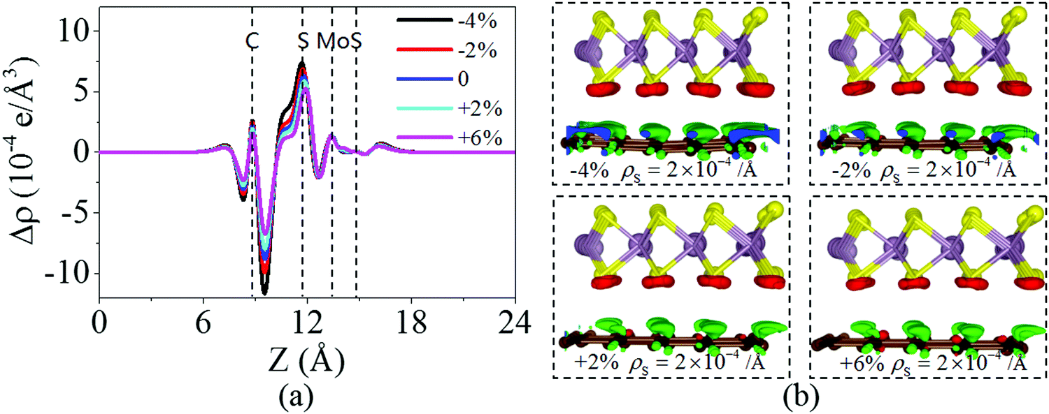
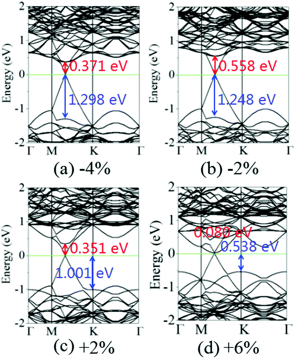
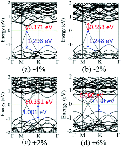
Fig. 6 shows the charge density difference of the graphene/MoS2 heterostructure under the biaxial strain. It is found that the fluctuation of the differential charge density curve decreases when the biaxial strain changes from −4% to +6%, indicating the less charge transfers from the graphene layer to MoS2 layer [Fig. 6(a)]. The same phenomenon can observe through the three dimensional isosurface of the charge density difference of the graphene/MoS2 heterostructure as shown in Fig. 6(b). According to Mulliken charge analysis, 0.062 e, 0.059 e, 0.055 e, and 0.051 e are transferred from the graphene layer to the MoS2 layer under a biaxial strain of −4%, −2%, +2%, and +6%, respectively. Thus, by applying biaxial strain, the interlayer distance and charge density difference change slightly. However, there is an obvious change in the electronic structure of the graphene/MoS2 heterostructure by applying the biaxial strain. Although the electronic band structures of pristine graphene is still preserved, the band structure of MoS2 substantial changes under the biaxial strain. In particular, the band gaps of the MoS2 layer in the heterostructure are 1.669 eV, 1.806 eV, 1.352 eV, and 0.618 eV under a biaxial strain of −4%, −2%, +2%, and +6%, respectively (Fig. 7).
 |
| | Fig. 6 (a) Plane averaged charge density differences and (b) three dimensional isosurface of the charge density difference of the graphene/MoS2 heterostructure under a biaxial strain. | |
 |
| | Fig. 7 Band structures of the graphene/MoS2 heterostructure under a biaxial strain: (a) −4%, (b) −2%, (c) +2%, and (d) +6%. | |
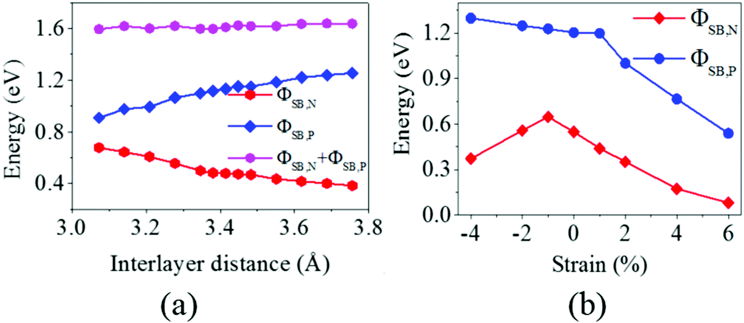
It is obvious that the graphene/MoS2 heterostructure is characterized by the metal/semiconductor heterostructure. In the graphene/MoS2 heterostructure, the n-type Schottky barrier height (ΦSB,N) is ΦSB,N = ECBM − EF, whereas the p-type Schottky barrier height (ΦSB,P) is ΦSB,P = EF − EVBM. ECBM, EVBM, and EF represent the conduction band minimum, valence band maximum, and Fermi level, respectively. Fig. 8 displays the evolution of the n- and p-type Schottky barrier height (ΦSB,N and ΦSB,P) of the graphene/MoS2 heterostructure at the various interlayer distance and under the biaxial strain. When the interlayer distance is reduced, the ΦSB,N gradually increases, but ΦSB,P gradually decreases. Moreover, the value of ΦSB,P is always larger than that of ΦSB,N, indicating a n-type Schottky contact. The ΦSB,N values are 0.647 eV, 0.568 eV, 0.509 eV, and 0.418 eV when the interlayer distances are 3.209 Å, 3.346 Å, 3.482 Å, and 3.755 Å, respectively [Fig. 8(a)]. For applying the biaxial strain from −4% to +6%, the ΦSB,P gradually increases for the graphene/MoS2 heterostructure, while the ΦSB,N increases initially and then decreases [Fig. 8(b)]. Furthermore, the ΦSB,N is only 0.080 eV under a biaxial strain of +6%, indicating that the Ohmic contact is nearly formed.
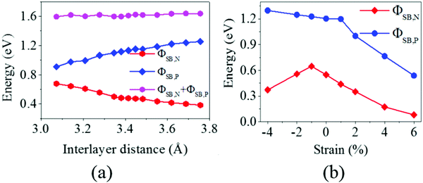 |
| | Fig. 8 The evolution of the n- and p-type Schottky barrier height (ΦSB,N and ΦSB,P) of the graphene/MoS2 heterostructure: (a) at various interlayer distances and (b) under a biaxial strain. | |
4. Conclusions
First principles calculations are performed to study the effects of the biaxial strain on the electronic properties and Schottky barrier of graphene/MoS2 heterostructures. It is found that the interlayer interaction is weakened and the charge transfer from the graphene layer to MoS2 layer is reduced with increasing interlayer distance, resulting in a shift of the Fermi level to a high energy state. The n-type Schottky barrier is formed with ΦSB,N values are 0.647 eV, 0.568 eV, 0.509 eV, and 0.418 eV when the interlayer distances are 3.209 Å, 3.346 Å, 3.482 Å, and 3.755 Å, respectively. The interlayer distance and charge density difference change slightly, while there is an obvious change in the electronic structure of the graphene/MoS2 heterostructure by applying the biaxial strain. For a biaxial strain of −4% to +6%, the ΦSB,P gradually increases for the graphene/MoS2 heterostructure, while the ΦSB,N increases initially and then decreases. Furthermore, the ΦSB,N is only 0.080 eV under a biaxial strain of +6%, indicating that the Ohmic contact is nearly formed. Our results provide a detailed understanding of the interfacial properties of graphene/MoS2 heterostructures and help to predict the performance of 2D material-based devices.
Conflicts of interest
There are no conflicts to declare.
Acknowledgements
This work was jointly supported by the Doctoral Program of Xi'an Polytechnic University (Grant No. 107020519 and 107020534), the National Natural Science Foundation of China (Grant No. 11674264 and 51771144), and the Natural Science Foundation of Shaanxi Province (Grant No. 2019TD-020, 2017JZ015, 2019JM-083, 2020JQ-823 and 2019JLM-30). This work was carried out using the HPCC platform at Xian Jiaotong University.
References
- K. S. Novoselov, A. K. Geim, S. V. Morozov, D. Jiang, Y. Zhang, S. V. Dubonos, I. V. Grigorieva and A. A. Firsov, Science, 2004, 306, 666–669 CrossRef CAS.
- A. K. Geim and K. S. Novoselov, Nat. Mater., 2007, 6, 183–191 CrossRef CAS.
- Y. D. Ma, Y. Dai, M. Guo, C. N. Niu, L. Yu and B. B. Huang, Nanoscale, 2011, 3, 2301–2306 RSC.
- Y. Wu, Y. Lin, A. A. Bol, K. A. Jenkins, F. Xia, D. B. Farmer, Y. Zhu and P. Avouris, Nature, 2011, 472, 74–78 CrossRef CAS.
- L. Liao, Y. C. Lin, M. Bao, C. Rui, J. Bai, Y. Liu, Y. Qu, K. L. Wang, Y. Huang and X. Duan, Nature, 2010, 467, 305–308 CrossRef CAS.
- Y. Xie, S. Cao, X. Wu, B. Y. Yu, L. Y. Chen and J. M. Zhang, Physica E, 2020, 124, 114252 CrossRef CAS.
- S. J. Haigh, A. Gholinia, R. Jalil, S. Romani, L. Britnell, D. C. Elias, K. S. Novoselov, L. A. Ponomarenko, A. K. Geim and R. Gorbachev, Nat. Mater., 2012, 11, 1–4 CrossRef.
- C. R. Dean, A. F. Young, I. Meric, C. Lee, L. Wang, S. Sorgenfrei, K. Watanabe, T. Taniguchi, P. Kim, K. L. Shepard and J. Hone, Nat. Nanotechnol., 2010, 5, 722–726 CrossRef CAS.
- K. S. Novoselov, Rev. Mod. Phys., 2011, 83, 837–849 CrossRef CAS.
- S. Wang, C. Ren, H. Tian, J. Yu and M. Sun, Phys. Chem. Chem. Phys., 2018, 20, 13394–13399 RSC.
- S. Wang, H. Tian, C. Ren, J. Yu and M. Sun, Sci. Rep., 2018, 8, 12009 CrossRef.
- S. Wang, N. T. Hung, H. Tian, M. S. Isiam and R. Saito, Phys. Rev. Appl., 2021, 16, 024030 CrossRef CAS.
- Y. Liu, R. Cheng, L. Liao, H. L. Zhou, J. W. Bai, G. Liu, L. X. Liu, Y. Huang and X. F. Duan, Nat. Commun., 2011, 2, 579 CrossRef.
- T. J. Echtermeyer, L. Britnell, P. K. Jasnos, A. Lombardo, R. V. Gorbachev, A. N. Grigorenko, A. K. Geim, A. C. Ferrari and K. S. Novoselov, Nat. Commun., 2011, 2, 458 CrossRef CAS.
- W. J. Yu, Y. Liu, H. L. Zhou, A. X. Yin, Z. Li, Y. Huang and X. F. Duan, Nat. Nanotechnol., 2013, 8, 952 CrossRef CAS.
- K. Roy, M. Padmanabhan, S. Goswami, T. P. Sai, G. Ramalingam, S. Raghavan and A. Ghosh, Nat. Nanotechnol., 2013, 8, 826 CrossRef CAS PubMed.
- J. Y. Kwak, J. Hwang, B. Calderon, H. Alsalman, N. Munoz, B. Schutter and M. G. Spencer, Nano Lett., 2014, 14, 4511–4516 CrossRef CAS PubMed.
- L. L. Yu, Y. H. Lee, X. Ling, E. J. G. Santos, Y. C. Shin, Y. X. Lin, M. Dubey, E. Kaxiras, J. Kong, H. Wang and T. Palaxios, Nano Lett., 2014, 14, 3055–3063 CrossRef CAS.
- C. Lee, X. Wei, J. W. Kysar and J. Hone, Science, 2008, 321, 385 CrossRef CAS PubMed.
- K. Yin, T. Huang, H. Y. Wu, Y. Si, J. C. Lian, Y. W. Xiao, Z. Zhang, W. Q. Huang, W. Hu and G. F. Huang, J. Phys. D: Appl. Phys., 2021, 54, 265302 CrossRef CAS.
- T. Huang, Q. Chen, M. Q. Cheng, W. Q. Huang, W. Hu and G. F. Huang, J. Phys. D: Appl. Phys., 2019, 52, 305104 CrossRef CAS.
- S. Bertolazzi, J. Brivio and A. Kis, ACS Nano, 2011, 5, 9703–9709 CrossRef CAS.
- A. Castellanos−Gomez, M. Poot, G. A. Steele, H. S. J. van der Zant, N. Agraït and G. Rubio−Bollinger, Adv. Mater., 2012, 24, 772 CrossRef.
- J. Pu, Y. Yomogida, K. K. Liu, L. J. Li, Y. Iwasa and T. Takenobu, Nano Lett., 2012, 12, 4013–4017 CrossRef CAS PubMed.
- J. W. Jiang and H. S. Park, Appl. Phys. Lett., 2014, 105, 033108 CrossRef.
- H. Zhang, D. Wu, Q. Tang, L. Liu and Z. Zhou, J. Mater. Chem. A, 2013, 1, 2231–2237 RSC.
- H. Zhang, Y. Li, Q. Tang, L. Liu and Z. Zhou, Nanoscale, 2012, 4, 1078–1084 RSC.
- I. Shahid, S. Ahmad, N. Shehzad, S. Yao, C. V. Nguyen, L. Zhang and Z. Zhou, Appl. Surf. Sci., 2020, 523, 146483 CrossRef CAS.
- N. Shehzad, I. Shahid, S. Yao, S. Ahmad, A. Ali, L. Zhang and Z. Zhou, Int. J. Hydrogen Energy, 2020, 45, 27089–27097 CrossRef CAS.
- G. Kresse and J. Hafner, Phys. Rev. B: Condens. Matter Mater. Phys., 1993, 47, 558–561 CrossRef CAS.
- G. Kresse and J. Hafner, Phys. Rev. B: Condens. Matter Mater. Phys., 1994, 49, 14251–14269 CrossRef CAS.
- P. E. Blöchl, Phys. Rev. B: Condens. Matter Mater. Phys., 1994, 50, 17953–17979 CrossRef PubMed.
- J. P. Perdew, K. Burke and M. Ernzerhof, Phys. Rev. Lett., 1996, 77, 3865–3868 CrossRef CAS.
- S. Grimme, J. Comput. Chem., 2006, 27, 1787–1799 CrossRef CAS.
- K. Momma and F. Izumi, J. Appl. Crystallogr., 2008, 41, 653–658 CrossRef CAS.
- Y. D. Ma, Y. Dai, M. Guo, C. W. Niu and B. B. Huang, Nanoscale, 2011, 3, 3883–3887 RSC.
- W. Hu, T. Wang, R. Zhang and J. Yang, J. Mater. Chem. C, 2016, 4, 1776–1781 RSC.
- J. E. Padilha, A. Fazzio and A. J. R. da Silva, Phys. Rev. Lett., 2015, 114, 066803 CrossRef CAS PubMed.
- W. Hu, T. Wang and J. Yang, J. Mater. Chem. C, 2015, 3, 4756–4761 RSC.
- B. Liu, L. J. Wu, Y. Q. Zhao, L. Z. Wang and M. Q. Cai, Phys. Chem. Chem. Phys., 2016, 18, 19918–19925 RSC.
- Y. Cai, G. Zhang and Y. W. Zhang, J. Phys. Chem. C, 2015, 119, 13929–13936 CrossRef CAS.
- C. Xia, B. Xue, T. Wang, Y. Peng and Y. Jia, Appl. Phys. Lett., 2015, 107, 193107 CrossRef.
- Y. Wang and Y. Ding, Phys. Chem. Chem. Phys., 2015, 17, 27769–27776 RSC.
- W. J. Zhang, C. P. Chu, J. K. Huang, C. H. Chen, M. L. Tsai, Y. H. Chang, C. T. Liang, Y. Z. Chen, Y. L. Chueh, J. H. He, M. Y. Chou and L. J. Li, Sci. Rep., 2014, 4, 3826 CrossRef.
- S. Tongay, W. Fan, J. Kang, J. Park, U. Koldemir, J. Suh, D. S. Narang, K. Liu, J. Ji, J. Li, R. Sinclair and J. Wu, Nano Lett., 2014, 14, 3185–3190 CrossRef CAS.
- M. Dienwiebel, G. S. Verhoeven, N. Pradeep, J. W. M. Frenken, J. A. Heimberg and H. W. Zandbergen, Phys. Rev. Lett., 2004, 92, 126101 CrossRef PubMed.
- S. Clark, K. J. Jeon, J. Y. Chen and C. S. Yoo, Solid State Commun., 2013, 154, 15–18 CrossRef CAS.
- H. J. Conley, B. Wang, J. I. Ziegler, R. F. J. Haglund, S. T. Pantelides and K. I. Bolotin, Nano Lett., 2013, 13, 3626–3630 CrossRef CAS.
- P. Johari and V. B. Shenoy, ACS Nano, 2012, 6, 5449–5456 CrossRef CAS.
- L. Wang, A. Kutana and B. I. Yakobson, Ann. Phys., 2014, 526, L7–L12 CrossRef CAS.
- S. Wang, M. S. Ukhtary and R. Saito, Phys. Rev. Res., 2020, 2, 033340 CrossRef CAS.
- P. Johari and V. B. Shenoy, ACS Nano, 2012, 6, 5449–5456 CrossRef CAS.
|
| This journal is © The Royal Society of Chemistry 2022 |
Click here to see how this site uses Cookies. View our privacy policy here. 
 Open Access Article
 This Open Access Article is licensed under a Creative Commons Attribution-Non Commercial 3.0 Unported Licence
 ab,
Min
Li
a,
Xumei
Zhao
a,
Lin
Yuan
a,
Boyu
Wang
a,
Caijuan
Xia
*a and
Fei
Ma
ab,
Min
Li
a,
Xumei
Zhao
a,
Lin
Yuan
a,
Boyu
Wang
a,
Caijuan
Xia
*a and
Fei
Ma