
 Open Access Article
 This Open Access Article is licensed under a
 Creative Commons Attribution 3.0 Unported Licence
Effect of PEDOT:PSS on the performance of solution-processed blue phosphorescent organic light-emitting diodes with an exciplex host†
Jaber
Saghaei
a,
Manikandan
Koodalingam
 a,
Paul L.
Burn
*a,
Ian R.
Gentle
a,
Almantas
Pivrikas
b and
Paul E.
Shaw
a
a,
Paul L.
Burn
*a,
Ian R.
Gentle
a,
Almantas
Pivrikas
b and
Paul E.
Shaw
a
aCentre for Organic Photonics & Electronics (COPE), School of Chemistry and Molecular Biosciences, The University of Queensland, Brisbane, Queensland 4072, Australia. E-mail: p.burn2@uq.edu.au
bSchool of Engineering and Information Technology, Murdoch University, Perth, Western Australia 6150, Australia
First published on 3rd December 2021
Abstract
In this study, efficient solution-processed organic light-emitting diodes (OLEDs) based on a light-emitting layer composed of a blue emissive phosphorescent dendrimer and exciplex host were investigated. Employing poly(styrene sulfonic acid) doped poly(ethylenedioxythiophene):poly(styrenesulfonate) (m-PEDOT:PSS) as the hole injection layer resulted in devices with external quantum efficiencies (EQEs) over 20% for luminances of up to 100 cd m−2. A feature of these devices was a relatively slow electroluminescence turn-on for the initial voltage scan, which was absent when m-PEDOT:PSS was replaced with molybdenum oxide as the hole injection layer. The initial turn-on rate was found to decrease with increasing PSSH content, with the results suggesting that proton migration from (m-)PEDOT:PSS is the cause of the change in the device performance. The overall device performance was found to be scan dependent, with sequential voltage scans leading to a decrease in EQE, which is ascribed at least in part to electromer formation. We also demonstrate solution-processed OLEDs with the same exciplex host and bis[2-(4,6-difluorophenyl)pyridinato-C2,N](picolinato)iridium(III) (FIrpic) as the emitter, that have maximum EQE and power efficiencies of 17.0% and 25.3 lm W−1, respectively.
Introduction
Films of exciplex-forming materials have given rise to organic light-emitting diodes (OLEDs) with good efficiencies either as emissive layers or as hosts for phosphorescent, thermally activated delayed fluorescence (TADF), or fluorescent emitters.1–9 A reported feature of bulk exciplex films when used as a host for guest emitters is their ambipolarity,10 which arises from the fact that they are composed of a blend of low ionisation potential (donor) and high electron affinity (acceptor) materials. The blend of the two materials has been observed to reduce both the operating voltage and efficiency roll-off, which in the case of the latter has been attributed to the placement and broadening of the recombination zone in the emissive layer. A potential advantage of bulk exciplex films, and their covalently linked analogues (TADF materials), is that they can be designed to have sufficiently high singlet and triplet energies with small singlet and triplet energy gaps (ΔEST) to prevent energy back transfer from the emissive guest. An advantage of exciplex blends over TADF materials as hosts is that they can be formed by simply blending two materials, thus enabling many different materials combinations and ratios to be investigated.11 The majority of exciplex blend host studies have focussed on films that are deposited by vacuum evaporation with there being few reports of solution processed exciplex host-based OLEDs.12,13While the creation of exciplex host blends for green and red guest emitters is relatively straightforward, it is more difficult to create donor–acceptor combinations that form suitable hosts for blue emissive materials,14 and in particular, solution-processed blue phosphorescent emitters. The emission energy of the exciplex host is governed by the ionisation potential of the donor and the electron affinity of the acceptor and hence there needs to be a sufficiently large energy offset such that neither component of the exciplex host nor the formed exciplex quench the triplet state of the blue emitter. In the context of solution processed blue-phosphorescent emitters, there have been a number of reports of exciplex hosts composed of 4,4′,4′′-tris(carbazol-9-yl)triphenylamine (TCTA) (donor) (and derivatives) and phosphine oxide-based acceptors with bis[2-(4,6-difluorophenyl)pyridinato-C2,N](picolinato)iridium (III) (FIrpic) as the emitter.15–19 In fact, most reports describing solution-processed bulk exciplex hosts for blue emissive guests include the use of phosphine oxide derivatives as the acceptor in the blend, which is due to their relatively small electron affinities and high triplet energies.15 The best performing of these thus far had a device architecture of ITO/PEDOT:PSS/Ph–O–TCTA:PhPO:FIrpic/TPBI/Cs2CO3/Al [PEDOT:PSS = poly(ethylenedioxythiophene):poly(styrenesulfonate), Ph–O–TCTA = a tris–TCTA based macromolecule, PhPO = tris[4-(diphenylphosphoryl)phenyl]benzene, TPBI = 2,2′,2′′-[1,3,5-benzinetriyl]-tris[1-phenyl-1-H-benzimidazole], Cs2CO3 = caesium carbonate, Al = aluminium] giving an external quantum efficiency of 16.5%, and power (PE) and current (CE) efficiencies of 20.6 lm W−1 and 33.6 cd A−1, respectively.19 However, one of the issues of developing solution-processed blue phosphorescent-exciplex host films is that many of the available materials have been developed for evaporative processing and do not always form good quality films from solution. For example, solution processed films of FIrpic generally contain aggregates.20–23 In early work on solution processed phosphorescent OLEDs it was shown that light-emitting dendrimers could form good quality films when blended with host materials that had poor solubility and propensity to aggregate when deposited from solution.24 In this paper we show that a blue phosphorescent light-emitting dendrimer, Ir(DTri)3, blended with a TCTA:POPH exciplex host (see Fig. 1 for structures) can be solution processed to form films of good quality. The choice of a TCTA:POPH blend as the exciplex host was based on the fact that it had been successfully used for FIrpic and that Ir(DTri)3 was also a sky blue emitter. Furthermore, we report and discuss the photophysical, electronic and device properties of the blend emissive films and compare the device performance with films using FIrpic as the emissive material.
 | ||
| Fig. 1 Structures of TCTA, POPH, Ir(DTri)3, FIrpic, and the electron transport/hole blocking BP4mPy used in the bilayer devices. | ||
Results and discussion
Photophysical and electrical properties
We first investigated the photophysical properties of the neat exciplex films and those blended with 5-fac-tris[4′′-(t-butyl)-5′-{4-[t-butyl]phenyl}-4′-methyl-(1,1′:3′,1′′-terphenyl)-3-yl]-1-methyl-3-propyl-1H-1,2,4-triazolyl]iridium(III) [Ir(DTri)3]. A 1:1 molar ratio of the TCTA and [5-terphenyl-1,3-phenylene]bis[diphenylphosphine oxide] (POPH) was chosen so that in principle every donor had its own acceptor. Films were prepared from dichloromethane solutions to ensure that both the TCTA and POPH were dissolved. The film absorption spectrum of the 1:1 molar ratio of TCTA and POPH was found to be a linear combination of the individual TCTA and POPH absorption spectra (Fig. S1, ESI†). Therefore, to a first approximation no ground state interactions (aggregation or charge transfer state formation) were observed between the TCTA and POPH in blend.25,26 The PL spectra of TCTA, POPH, the 1:1 TCTA:POPH blend and the blend containing Ir(DTri)3 are shown in Fig. 2. POPH has a featureless PL emission that is at a shorter wavelength than TCTA, which is consistent with the higher energy absorption onset. The 1:1 TCTA:POPH blend film had a broad PL feature associated with the exciplex emission, with a shoulder clearly visible on the high energy side. The broad and featureless PL emission of an exciplex is due to the existence of various emissive species in the blend.10 The shoulder at shorter wavelengths of around 385 nm indicates there was emission from TCTA as well as the exciplex, which was confirmed by exciting the film at 330 nm where the TCTA absorbs but POPH does not (see Fig. S1, ESI†). However, exciting the film at 270 nm excites both the POPH and TCTA (which are in a 1:1 molar ratio) and it can be seen in Fig. 2 that in addition to the exciplex and TCTA emission there was small component of the emission at 355 nm, which is consistent with POPH emission. Thus, in spite of the donor and acceptor materials being in a 1:1 molar ratio, not all the emission is exciplex-based, which is suggestive of a degree of phase separation in the spin-coated film.27 | ||
| Fig. 2 Absorption spectrum of Ir(DTri)3 and PL spectra of the individual components and blends (1:1 molar ratio TCTA:POPH and 20 wt% Ir(DTri)3 in TCTA:POPH at a 1:1 molar ratio – λexc = 330 nm and λexc(POPH) = 270 nm). In terms of calculating the weight percent (wt%) of Ir(DTri)3 in the film, the TCTA and POPH are taken as a combined weight. That is, the film with 20 wt% Ir(DTri)3 has 80 wt% of the 1:1 molar ratio of TCTA and POPH. Note the neat TCTA PL spectrum has a broad emission out to around 600 nm, which arises from aggregate/excimer emission. | ||
The PL emission of the 20 wt% Ir(DTri)3 in a 1:1 molar ratio TCTA:POPH film is also shown in Fig. 2. At first glance it appears that at an excitation wavelength of 330 nm only emission from Ir(DTri)3 is observed. Indeed, Fig. S2a (ESI†) shows that the PL spectrum is independent of the excitation wavelength (250–350 nm). However, plotting the PL spectra on a logarithmic scale, Fig. S2b (ESI†), it can be seen that even up to a concentration of 30 wt% Ir(DTri)3 there is still a small component of host emission.
The PL quantum yields (PLQYs) of films with different dendrimer concentrations are summarised in Fig. 3. The exciplex host films (with no guest) had a low PLQY of 3 ± 1%. The PLQY was found to reach a maximum of 67 ± 6% for a dendrimer concentration of 20 wt% with the neat dendrimer film having a PLQY of 16 ± 2%. The solution PLQY of the dendrimer is 73 ± 8%, which was close to that of the 20 wt% dendrimer blend film, indicating that the dendrimers are not strongly interacting with each other in the exciplex host at that concentration.28–30
 | ||
| Fig. 3 (a) PLQYs of films with different dendrimer concentrations. (b) TRPL decays of Ir(DTri)3 in solution, films of the exciplex host or dendrimer, and exciplex films containing different concentrations of the dendrimer. | ||
In the final part of the study on the PL properties we measured the PL decays of the exciplex TCTA:POPH blend and Ir(DTri)3 films, and films containing different concentrations of Ir(DTri)3 (Fig. 3b, with the lifetime fitting parameters for the exciplex host, neat dendrimer and 20 wt% dendrimer blend summarised in Table S1, ESI†). The PL decay of Ir(DTri)3 in solution is also shown for comparison. In solution, Ir(DTri)3 had a mono-exponential decay with a lifetime of 4.1 μs, which is consistent with an absence of interchromophore interactions. The 1:1 molar ratio TCTA:POPH blend film was found to have a multi-exponential decay with a lifetime longer than that of individual films of TCTA and POPH, which again confirms exciplex emission from the host film. The neat Ir(DTri)3 also had a multi-exponential decay, with the largest component having a lifetime shorter than that measured in solution. These characteristics are consistent with there being intermolecular interchromophore interactions that lead to the quenching of the luminescence in the neat Ir(DTri)3 film. The film PL lifetimes were found to decrease with increasing Ir(DTri)3 concentration, with the neat film of Ir(DTri)3 having the shortest. These results are consistent with the PLQY measurements and an increase in intermolecular interchromophore interactions between the emissive Ir(DTri)3 macromolecules with increasing guest concentration in the mixed exciplex host.
Prior to fabricating and testing OLEDs containing the emissive layer materials, we measured their hole and electron mobilities using metal–insulator–semiconductor charge extraction by linearly increasing voltage (MIS-CELIV) and photo-MIS-CELIV, respectively (Fig. S3 shows the transients, ESI†). The neat film of Ir(DTri)3 had a hole mobility of (9.6 ± 0.7) × 10−5 cm2 V−1 s−1 and the exciplex blend film had hole and electron mobilities of (1.1 ± 0.3) × 10−6 and (8.5 ± 1.3) × 10−7 cm2 V−1 s−1, respectively. The similarity of the electron and hole mobilities of the TCTA:POPH blend film demonstrates the ambipolar charge transport characteristics and its suitability as a host. The electron [(8.0 ± 1.2) × 10−8 cm2 V−1 s−1] and hole [(4.9 ± 0.8) × 10−7 cm2 V−1 s−1] mobilities of the emissive layer containing 20 wt% of Ir(DTri)3 were lower than those of the TCTA:POPH blend, which is consistent with the Ir(DTri)3 trapping the charges.31,32
Exciplex organic light-emitting diodes
We fabricated OLEDs with the structure ITO/PEDOT:PSS/(1:1)TCTA:POPH:Ir(DTri)3/BP4mPy/LiF/Al [BP4mPy = 3,3′,5,5′-tetra[(m-pyridyl)-phen-3-yl]biphenyl, LiF = lithium fluoride] with different wt% of Ir(DTri)3 in the TCTA:POPH (1:1 molar ratio) host with the results shown in Fig. 4 and Table S2 (ESI†) summarising the key device performance parameters. The highest external quantum efficiency (EQE) was observed for the devices containing emissive layers with 20 wt% of the Ir(DTri)3, which corresponded to the blend ratio with the highest PLQY (Fig. 3a). For each blend ratio the EQE was found to generally increase with luminance (L) indicating unbalanced charge injection and transport at low luminance.33,34 That being said, at a luminance of 130 cd m−2 the EQE of 12.1% for the device with 20 wt% Ir(DTri)3, was close to the theoretical maximum of 13.5% based on a film PLQY of 67 ± 6% and the standard outcoupling of around 20% for a bottom emitting device.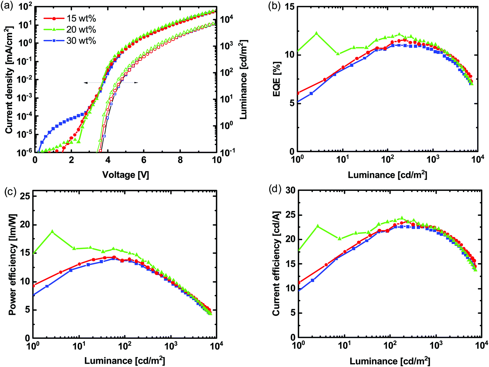 | ||
| Fig. 4 (a) J–V–L, (b) EQE–L, (c) PE–L and (d) CE–L of OLEDs with the structure of ITO/PEDOT:PSS/TCTA:POPH:Ir(DTri)3/BP4mPy/LiF/Al with different Ir(DTri)3 wt% and a TCTA:POPH molar ratio of 1:1. | ||
It has been reported that adding poly(4-styrenesulfonic acid) (PSSH) to PEDOT:PSS (m-PEDOT:PSS) can increase the work function from 5.04 eV to 5.59 eV and improve hole injection.35 We therefore used m-PEDOT:PSS in place of PEDOT:PSS in the devices with 20 wt% of Ir(DTri)3 in the emissive layer with the results shown in Fig. 5 and the OLED performance characteristics summarised in Table S2 (ESI†). Addition of the PSSH to PEDOT:PSS led to a dramatic difference in the EQE at low luminance for the first voltage scan, with the EQE reaching more than 20% at a luminance of up to around 20 cd m−2. This performance was repeatable on multiple pixels (see Table S2, ESI†). However, at luminances of ≥100 cd m−2 the EQE for the m-PEDOT:PSS containing OLED was similar to that of devices that used pristine PEDOT:PSS (cf. Fig. S4 and S5, ESI†). To determine whether the high initial EQE was dependent on the trap density arising from the emitter concentration we also prepared a device with a smaller Ir(DTri)3 component. However, a high initial EQE was still observed when the Ir(DTri)3 concentration in the emissive layer was reduced to 2 wt% (Fig. S4, ESI†). It should be noted that even though a high EQE was observed on the first scan, the PLQY values for all the emissive layers were less than 70%. To determine whether this phenomenon was due to the Ir(DTri)3 emitter being dendrimeric we also prepared devices with the same configuration but with 10 wt% of FIrpic as the emissive material (the known optimum guest ratio). We found a similar effect with the maximum EQE and PE reaching to 17.0% and 25.3 lm W−1, respectively, for the first scan, which is the highest reported thus far for solution processed exciplex OLEDs containing FIrpic (Fig. S5, ESI†). As with the Ir(DTri)3 containing devices, at higher luminance the performance of the OLEDs containing either PEDOT:PSS or m-PEDOT:PSS were similar (Fig. S5, ESI†).
 | ||
| Fig. 5 (a) J–V–L, (b) EQE–L, (c) PE–L and (d) CE–L of OLEDs with PEDOT:PSS or m-PEDOT:PSS as the hole injection layer and (1:1) TCTA:POPH:(20 wt%)Ir(DTri)3 as the emissive layer. | ||
At first sight the results of our OLEDs with the m-PEDOT:PSS seem to confirm the general improvement in performance previously reported. However, when we undertook several voltage scans, we found that the subsequent EQEs were lower (decreasing after the first scan before becoming relatively stable) than that measured on the first scan (note this effect was not highlighted in the published work).35 It is clear from the data in Fig. 6 that the first and subsequent voltage scans have different electrical and optical characteristics. A further observation we noted is that when the pixel was turned on and held at 4 V there was a delay in reaching uniform emission for devices composed of hole injection layers of either PEDOT:PSS or m-PEDOT:PSS (see Fig. 7), with the latter having a significantly slower turn-on. However, when the same pixel was turned off and then back on at 4.0 V there was no delay in illumination and the pixel had instant uniform emission.
 | ||
| Fig. 6 (a) J–V–L, (b) EQE–L (c) PE–L and (d) CE–L of an OLED with the structure ITO/m-PEDOT:PSS/(1:1)TCTA:POPH:(20 wt%)Ir(DTri)3/BP4mPy/LiF/Al for sequential voltage scans (S1–S6). | ||
 | ||
| Fig. 7 Photos of an OLED composed of m-PEDOT:PSS and Ir(DTri)3 blended into the exciplex host held at 4.0 V. | ||
The question therefore arises as to what are the origins of both the slow turn on and high EQEs for the first voltage scan. A high EQE in the first voltage scan could arise from one of the charge carriers filling traps in the emissive layer leading to a higher internal electric field that enhances the injection of the second carrier at low voltage. In subsequent scans, the charge traps would remain filled and thus the internal electric field would be reduced. Such a situation could be affected by the distribution of the components in the emissive layer. For example, vertical phase separation of the components could lead to a different trap and electric field profile compared to the case where the materials are evenly distributed throughout the film. To check whether the components in the emissive layer were uniformly distributed we undertook depth profiling X-ray Photoelectron Spectroscopy measurements on a glass/m-PEDOT:PSS/TCTA:POPH:(20 wt%)Ir(DTri)3 film stack (Fig. S6, ESI†). We found that based on the atomic percentages the ratio of the TCTA, POPH and Ir(DTri)3 was as expected from the ratio of the materials in the processing solution (Fig. S7a, ESI†). In addition, there was no evidence of vertical separation of any of the components (Fig. S7b, ESI†). This is in contrast to the reported accumulation of FIrpic at the PEDOT:PSS/EML interface36 and is evidence of the ability of the dendrimeric Ir(DTri)3 to provide the processability needed to form good quality uniform thin films.
To test whether the slow turn-on (see Fig. 7) arises from trapped charges we held a device after a positive voltage scan at a negative bias of −5 V for 10 minutes to attempt to depopulate the trap states and potentially restore the device to its original state. However, we found that there was no difference in the performance during the second positive voltage scan (Fig. S8, ESI†). In addition, the fact that the time required for a pixel to reach uniform emission on the first scan is on the order of seconds suggests that an alternative mechanism to charge trapping is giving rise to the effect, e.g., proton migration from the (m-)PEDOT:PSS into the emissive layer. To confirm that the PEDOT:PSS is primarily responsible for the effect we prepared equivalent (1:1) TCTA:POPH:(20 wt%)Ir(DTri)3 devices with molybdenum oxide (MoOx) as the hole injection layer. While the devices had lower overall performance (see Fig. S9, ESI†) there was no significant difference in the device characteristics between the first and subsequent voltage scans. Furthermore, the devices turned on instantaneously. Thus, differences in performance of the (m-)PEDOT:PSS devices between voltage scans arise from the conducting polymer layer itself.
To determine whether the amount of PSSH added to the PEDOT:PSS had an effect on the performance of the devices we varied the PSSH concentration. We found that independent of the amount of PSSH added the first voltage scan always gave a high EQE at low luminance, which was higher than that of the devices with pristine PEDOT:PSS (Fig. S10, ESI†). We also note that the delay in reaching uniform emission at an initial voltage of 4.0 V was dependent on the concentration of the PSSH in the m-PEDOT:PSS, with a greater amount of PSSH leading to a slower response. These results suggest that proton migration from (m-)PEDOT:PSS into the emissive layer is primarily responsible for the first scan performance. To see whether we could block proton transfer we followed a previous report where a poly(9-vinylcarbazole) (PVK) layer was deposited onto the PEDOT:PSS layer before depositing the emissive film from solution.37 The driving voltage was found to increase for the device containing the PVK layer, which indicated that it was present despite it being thin (< 15 nm). However, in our devices the PVK layer did not have a significant effect and a higher EQE was still observed for the first scan (Fig. S11, ESI†).
In addition to the electrical characteristics, we measured the electroluminescence (EL) spectra of the devices (Fig. 8). For the devices containing 20 wt% Ir(DTri)3 there was a small peak at 640 nm (note the log scale) in addition to the blue emission from the dendrimer. The peak at 640 nm was found to increase in intensity with multiple voltage scans. Previous reports of exciplex EL from TCTA:POPH blends have assigned the long wavelength peak to an electromer,16 and interestingly, in our work we did not observe the peak for the devices that had FIrpic as the emitter nor those with a MoOx hole injection layer (Fig. S5d and S9d, ESI†). We also observed the peak at 640 nm when the emissive layer only contained TCTA and Ir(DTri)3 (Fig. S12, ESI†), i.e., with no POPH, indicating the feature is not exciplex in origin and is consistent with a TCTA electromer.16 The formation of an electromer can provide an additional weakly radiative decay pathway, which can in part explain the observed reduction in device efficiency with increasing number of scans. The fact that the electromer emission was not observed for the devices that had MoOx as the hole injection layer suggests that the (m-)PEDOT:PSS plays a role in its formation.
 | ||
| Fig. 8 EL spectra of OLEDs on (a) PEDOT:PSS and (b) m-PEDOT:PSS for different voltage scans. S represents “scan” and the scan number is shown. | ||
Although it is difficult to elucidate the reason for the electromer formation, previous reports have shown that protons38,39 and even fragments of PSS36 can diffuse into the emissive layer. It is therefore not unreasonable to assume that these components could lead to the chemical changes of materials in the emissive layer that could lead to electromer formation or degradation of the materials. It is important to note that electromer formation has been previously reported to be irreversible and will in part impact device stability.16,40
Conclusion
In summary, high efficiency blue dendrimer OLEDs based on an exciplex host were demonstrated, with maximum EQEs exceeding 20% at light intensities up to around 20 cd m−2. The maximum external quantum efficiency was notably more than the theoretical estimate based on the film PLQY (which was 67 ± 6%) and standard outcoupling of 20% for a bottom emitting device. However, the very high efficiency was only observed for the first voltage scan with subsequent voltage ramps giving a lower efficiency than the first. A feature of the devices was that there was a delay in the pixels achieving uniform emission when first measured. For subsequent measurements uniform emission was promptly observed above the turn-on voltage. Furthermore, it was found that a weakly emissive electromer formed during multiple voltage scans, which might in part explain the efficiency loss relative to the first scan. The changes in performance were not found when MoOx was used as the hole injection layer and hence we conclude that the PEDOT:PSS, particularly when doped with additional PSS, was the cause of the unusual device characteristics. Hence, we believe it is important that reports concerning OLEDs include data for higher scan numbers in addition to the first scan, particularly when (m-)PEDOT:PSS is used as the hole injection layer.Experimental section
Material information
Poly(ethylenedioxythiophene):poly(styrenesulfonate) (PEDOT:PSS aqueous solution – Clevios Al 4083 Ltd) was purchased from Ossila Ltd, 4,4′,4′′-tris[carbazol-9-yl]triphenylamine (TCTA), [5-terphenyl-1,3-phenylene]bis[diphenylphosphine oxide] (POPH), 3,3′,5,5′-tetra[(m-pyridyl)-phen-3-yl]biphenyl (BP4mPy) were purchased from Luminescence Technology Corp and poly(4-styrenesulfonic acid) (PSSH) solution (18 wt% in H2O, Mw ≈ 75![[thin space (1/6-em)]](https://www.rsc.org/images/entities/char_2009.gif) 000 g mol−1) was purchased from Sigma Aldrich. The synthesis of Ir(DTri)3 has been previously reported.41
000 g mol−1) was purchased from Sigma Aldrich. The synthesis of Ir(DTri)3 has been previously reported.41
Photophysical properties
UV-vis and photoluminescence (PL) spectra of films on fused silica substrates were measured using Cary 5000 UV-Vis-NIR and Jobin-Yvon Horiba Fluoromax 4 spectrometers, respectively. Films were prepared by spin-coating the mixtures at a concentration of 20 mg mL−1 in distilled and degassed dichloromethane at 2000 rpm before annealing at 100 °C for 30 min. Time-correlated single photon counting (TCSPC) measurements were undertaken using a Jobin-Yvon Florolog 3 spectrometer, with a pulsed LED (Horiba NanoLED). Photoluminescence quantum yields (PLQYs) were measured using an integrating sphere, coupled with an He–Cd laser with 325 nm excitation and beam power of around 0.2 mW. The measurements were undertaken with the sample held under a nitrogen atmosphere.Charge mobility
Hole and electron mobilities were obtained using metal–insulator–semiconductor charge extraction by linearly increasing voltage (MIS-CELIV)42 and photo-MIS-CELIV methods,43 respectively. The device structure for hole mobility was ITO/cyclotene 3022-35 (BCB, Dow Chemical Company) (30 nm)/MgF2 (50 nm)/emissive layer/MoOx (8 nm)/Ag (100 nm) with the ITO connected to the function generator (Agilent 33250A from Aglient technologies Inc.). The device structure for the electron mobility measurements was ITO/BCB (30 nm)/MgF2 (50 nm)/emissive layer/Al (100 nm) with the ITO connected to the oscilloscope (Waverunner 6200A from LeCroy corporation).The BCB solution in mesitylene (Sigma-Aldrich 98%) was diluted 1:10 by volume with mesitylene, and the solution was spin-coated at 5000 rpm in a glove box (O2 and H2O < 0.1 ppm) before annealing at 300 °C for 10 min. The substrates were then transfer to a vacuum evaporation chamber (MBRAUN and 10−6 mbar) for deposition of 50 nm MgF2. The emissive layers were spin-coated from 20 mg mL−1 solutions in distilled degassed dichloromethane at 2000 rpm and then annealed at 100 °C for 30 min to give films with a thickness of ≈150 nm. Finally, the samples were transferred to the vacuum evaporation chamber for deposition of 100 nm Al for the photo-MIS-CELIV experiment or 8 nm MoOx and 100 nm Ag for the MIS-CELIV measurement. A High Efficiency VIOLET LED emitter (LZ1-10UB00-01U7 purchased from OSRAM SYLVANIA Inc.) with 385–410 nm emission and 80 mW power was used for photo-MIS-CELIV experiments. The mobility was calculated from the time for maximum current extraction using:
 | (1) |
XPS analysis
XPS experiments were performed using a Kratos Axis Supra instrument (Kratos Analytical Ltd). Monochromatic Al K-alpha (1486.6 eV) radiation was used as the excitation source. Spectra were collected in the hybrid lens mode, with an excitation power of 225 W and a pass energy of 160 eV. Depth profiling was performed using Ar1000+ clusters accelerated to a kinetic energy of 10 keV rastered in a 3 mm × 3 mm region. To minimize the effect of atmosphere and subsequent contamination, the sample was kept under a nitrogen atmosphere, except during transfer to the ultrahigh vacuum chamber of the spectrometer (less than 15 minutes). The Casa XPS software was used for spectral peak fitting.OLEDs fabrication
20 Ω □−1 patterned ITO (1.5 cm × 1.5 cm) was purchased from Xinyan Technology Ltd and cleaned using ultrasonication for 15 min in each of Alconox, de-ionised water, acetone and 2-propanol. After drying under a nitrogen flow and treatment with UV-ozone for 20 min, filtered PEDOT:PSS was spin-coated onto the ITO at 5000 rpm before being annealed at 150 °C for 15 min. The PEDOT:PSS layer was around 35 nm thick. The PSSH-modified PEDOT:PSS (m-PEDOT:PSS) was prepared following the literature method.35 Briefly the aqueous poly(4-styrenesulfonic acid) (PSSH) was diluted with de-ionised water in a 10% volume ratio and then mixed with the PEDOT:PSS solution in a 50% volume ratio. For deposition of the emissive layer or PVK, the (m-)PEDOT:PSS coated substrates were transferred to a glove box with O2 < 0.3 ppm and H2O < 0.1 ppm. PVK (7.5 mg mL−1) in distilled chloroform was spin-coated at 5000 rpm onto the (m-)PEDOT:PSS layer and annealed at 120 °C for 20 min. The layer was then washed with chlorobenzene while being spun at 2500 rpm to remove any loose particles from the surface before annealing for 10 min at 120 °C. Emissive layers with a thickness of ≈55 nm were prepared by spin-coating the mixtures of the materials at a concentration of 10 mg mL−1 in distilled degassed dichloromethane at 3000 rpm before annealing at 100 °C for 30 min. The dichloromethane was dried over calcium hydride (CaH2) under an argon atmosphere before distillation and it was deoxygenated with three cycles of freeze–pump–thaw, backfilling with argon. Finally, a 45 nm BP4mPy electron transport layer and 1 nm LiF and 100 nm Al were deposited at rates of 1.0, 0.1 and 1.0 Å s−1, respectively in a thermal vacuum evaporation system (Kurt. J. Lesker SPECTROS evaporation system) with the initial pressure of 5 × 10⁻⁷ mbar. The current density–voltage–luminance (J–V–L) characteristics were measured in a nitrogen filled glovebox using a Keithley 2400 source meter coupled with an absolute EQE measurement system with a calibrated integrating sphere (Hamamatsu Photonics C9920-12).Conflicts of interest
There are no conflicts to declare.Acknowledgements
The work was carried at the Centre for Organic Photonics & Electronics at The University of Queensland. P. L. B. is an Australian Research Council Laureate Fellow (FL160100067) and the work was supported by the Fellowship. We would like to thank Associate Professor Lipton-Duffin of Central Analytical Research Facility, Queensland University of Technology, for the XPS measurements and assistance with their analysis.References
- P.-L. Zhong, C.-J. Zheng, M. Zhang, J.-W. Zhao, H.-Y. Yang, Z.-Y. He, H. Lin, S.-L. Tao and X.-H. Zhang, Org. Electron., 2020, 76, 105449 CrossRef CAS.
- J.-H. Lee, H. Shin, J.-M. Kim, K.-H. Kim and J.-J. Kim, ACS Appl. Mater. Interfaces, 2017, 9, 3277–3281 CrossRef CAS PubMed.
- S. Lee, K.-H. Kim, D. Limbach, Y.-S. Park and J.-J. Kim, Adv. Funct. Mater., 2013, 23, 4105–4110 CrossRef CAS.
- H. Lim, H. Shin, K.-H. Kim, S.-J. Yoo, J.-S. Huh and J.-J. Kim, ACS Appl. Mater. Interfaces, 2017, 9, 37883–37887 CrossRef CAS PubMed.
- Y. Seino, H. Sasabe, Y.-J. Pu and J. Kido, Adv. Mater., 2014, 26, 1612–1616 CrossRef CAS PubMed.
- M. Zhang, K. Wang, C.-J. Zheng, W. Liu, H. Lin, S.-L. Tao and X.-H. Zhang, Org. Electron., 2017, 50, 466–472 CrossRef CAS.
- Y.-T. Hung, Z.-Y. Chen, W.-Y. Hung, D.-G. Chen and K.-T. Wong, ACS Appl. Mater. Interfaces, 2018, 10, 34435–34442 CrossRef CAS PubMed.
- B. Zhao, T. Zhang, B. Chu, W. Li, Z. Su, H. Wu, X. Yan, F. Jin, Y. Gao and C. Liu, Sci. Rep., 2015, 5, 10697 CrossRef PubMed.
- C.-Y. Huang, S.-Y. Ho, C.-H. Lai, C.-L. Ko, Y.-C. Wei, J.-A. Lin, D.-G. Chen, T.-Y. Ko, K.-T. Wong and Z. Zhang, J. Mater. Chem. C, 2020, 8, 5704–5714 RSC.
- Y.-S. Park, S. Lee, K.-H. Kim, S.-Y. Kim, J.-H. Lee and J.-J. Kim, Adv. Funct. Mater., 2013, 23, 4914–4920 CrossRef CAS.
- P. L. dos Santos, F. B. Dias and A. P. Monkman, J. Phys. Chem. C, 2016, 120, 18259–18267 CrossRef CAS.
- B. Yao, X. Lin, B. Zhang, H. Wang, X. Liu and Z. Xie, J. Mater. Chem. C, 2018, 6, 4409–4417 RSC.
- K. Sun, Y. Sun, W. Tian, D. Liu, Y. Feng, Y. Sun and W. Jiang, J. Mater. Chem. C, 2018, 6, 43–49 RSC.
- M. Jung, K. H. Lee, J. Y. Lee and T. Kim, Mater. Horiz., 2020, 7, 559–565 RSC.
- Y.-X. Zhang, B. Wang, Y. Yuan, Y. Hu, Z.-Q. Jiang and L.-S. Liao, Adv. Opt. Mater., 2017, 5, 1700012 CrossRef.
- X. Ban, K. Sun, Y. Sun, B. Huang, S. Ye, M. Yang and W. Jiang, ACS Appl. Mater. Interfaces, 2015, 7, 25129–25138 CrossRef CAS PubMed.
- X. Ban, K. Sun, Y. Sun, B. Huang and W. Jiang, Org. Electron., 2016, 33, 9–14 CrossRef CAS.
- X. Ban, K. Sun, Y. Sun, B. Huang and W. Jiang, ACS Appl. Mater. Interfaces, 2016, 8, 2010–2016 CrossRef CAS PubMed.
- Y. Feng, T. Lu, D. Liu, W. Jiang and Y. Sun, Org. Electron., 2019, 67, 136–140 CrossRef CAS.
- Q. Wang and H. Aziz, Adv. Opt. Mater., 2015, 3, 967–975 CrossRef CAS.
- L. Liu, B. Zhang, Z. Xie, J. Ding and L. Wang, Org. Electron., 2013, 14, 55–61 CrossRef CAS.
- L. Liu, X. Liu, K. Wu, J. Ding, B. Zhang, Z. Xie and L. Wang, Org. Electron., 2014, 15, 1401–1406 CrossRef CAS.
- Y. You, S. H. Kim, H. K. Jung and S. Y. Park, Macromolecules, 2006, 39, 349–356 CrossRef CAS.
- S. C. Lo, N. A. H. Male, J. P. J. Markham, S. W. Magennis, P. L. Burn, O. V. Salata and I. D. W. Samuel, Adv. Mater., 2002, 14, 975–979 CrossRef CAS.
- C.-K. Moon, Molecular Orientation and Emission Characteristics of Ir Complexes and Exciplex in Organic Thin Films, Springer, 2019 Search PubMed.
- K.-H. Kim, C.-K. Moon, J. W. Sun, B. Sim and J.-J. Kim, Adv. Opt. Mater., 2015, 3, 895–899 CrossRef CAS.
- S. Wang, X. Wang, B. Yao, B. Zhang, J. Ding, Z. Xie and L. Wang, Sci. Rep., 2015, 5, 1–9 Search PubMed.
- X. Gong, J. C. Ostrowski, G. C. Bazan, D. Moses and A. J. Heeger, Appl. Phys. Lett., 2002, 81, 3711–3713 CrossRef CAS.
- F.-C. Chen, Y. Yang, M. E. Thompson and J. Kido, Appl. Phys. Lett., 2002, 80, 2308–2310 CrossRef CAS.
- B. Tong, Q. Mei, S. Wang, Y. Fang, Y. Meng and B. Wang, J. Mater. Chem., 2008, 18, 1636–1639 RSC.
- S. Sanderson, B. Philippa, G. Vamvounis, P. L. Burn and R. D. White, J. Chem. Phys., 2019, 150, 094110 CrossRef PubMed.
- M. Gao, T. Lee, P. L. Burn, A. E. Mark, A. Pivrikas and P. E. Shaw, Adv. Funct. Mater., 2020, 30, 1907942 CrossRef CAS.
- J. Saghaei, A. M. Brewer, W. Jiang, S. M. Russell, P. L. Burn and A. Pivrikas, Thin Solid Films, 2021, 718, 138475 CrossRef CAS.
- C. Murawski, K. Leo and M. C. Gather, Adv. Mater., 2013, 25, 6801–6827 CrossRef CAS PubMed.
- Y. Xiang, G. Xie, Q. Li, L. Xue, Q. Xu, J. Zhu, Y. Tang, S. Gong, X. Yin and C. Yang, ACS Appl. Mater. Interfaces, 2019, 11, 29105–29112 CrossRef CAS PubMed.
- K. F. Jeltsch, G. Lupa and R. T. Weitz, Org. Electron., 2015, 26, 365–370 CrossRef CAS.
- Y. Liu, X. Wei, Z. Li, J. Liu, R. Wang, X. Hu, P. Wang, Y. Yamada-Takamura, T. Qi and Y. Wang, ACS Appl. Energy Mater., 2018, 1, 543–551 CrossRef CAS.
- A. van Dijken, A. Perro, E. A. Meulenkamp and K. Brunner, Org. Electron., 2003, 4, 131–141 CrossRef CAS.
- J. Cameron and P. J. Skabara, Mater. Horiz., 2020, 7, 1759–1772 RSC.
- S. Kwon, K.-R. Wee, C. Pac and S. O. Kang, Org. Electron., 2012, 13, 645–651 CrossRef CAS.
- L. G. von Reventlow, W. Jiang, D. M. Stoltzfus, S. M. Russell, P. L. Burn and A. Colsmann, Adv. Opt. Mater., 2020, 8, 2001289 CrossRef CAS.
- M. Gao, P. L. Burn and A. Pivrikas, J. Appl. Phys., 2019, 126, 035501 CrossRef.
- M. Gao, P. L. Burn and A. Pivrikas, ACS Photonics, 2021, 8, 2425–2430 CrossRef CAS.
Footnote |
| † Electronic supplementary information (ESI) available. See DOI: 10.1039/d1ma00729g |
| This journal is © The Royal Society of Chemistry 2022 |