
 Open Access Article
 This Open Access Article is licensed under a Creative Commons Attribution-Non Commercial 3.0 Unported Licence
Oxygen vacancies in oxidized and reduced vertically aligned α-MoO3 nanoblades†
Sohaila Z.
Noby
*ab,
Azhar
Fakharuddin
a,
Stefan
Schupp
a,
Muhammad
Sultan
c,
Marina
Krumova
d,
Malte
Drescher
 d,
Mykhailo
Azarkh
d,
Klaus
Boldt
e and
Lukas
Schmidt-Mende
*a
d,
Mykhailo
Azarkh
d,
Klaus
Boldt
e and
Lukas
Schmidt-Mende
*a
aDepartment of Physics, University of Konstanz, 78467 Konstanz, Germany. E-mail: lukas.schmidt-mende@uni-konstanz.de
bDepartment of Solid-State Physics, National Research Centre (NRC), 12622 Cairo, Egypt
cNanoscience and Technology Department, National Centre for Physics, 440000 Islamabad, Pakistan
dDepartment of Chemistry, University of Konstanz, 78467 Konstanz, Germany
eDepartment of Chemistry & Zukunftskolleg, University of Konstanz, 78467 Konstanz, Germany
First published on 4th March 2022
Abstract
Functionalized materials are highly desired for technological advancements spanning physics, chemistry, materials science, and biology due to their unique electronic properties. One such example is molybdenum trioxide (MoO3), a metal oxide with multiple oxidation states. Manipulating these oxidation states can alter the electronic properties, for instance, defects and electrical conductivity, by several orders of magnitude. In this work, oxygen vacancy-mediated intrinsic defects in vertically aligned α-MoO3 crystals are systematically tuned via thermal treatment under different reducing and oxidizing atmospheres. The positions and the concentration of the oxygen vacancies and restitution of the oxygen ions have been experimentally demonstrated via a range of techniques including electron paramagnetic resonance, X-ray diffraction, and high-resolution electron microscopy. The calculated concentration of the oxygen vacancies in the α-MoO3−xvia EPR measurements is in the range of x = 0.004–0.049. The mechanism of the formation of oxygen vacancies in the α-MoO3−x crystal is understood via color center formation and polaron migration models. These oxygen vacancies show no influence on the optical band gap. However, they significantly impact the electrical conductivity on the order of 102 Sm−1 by altering the MoO3 properties from semi-insulating to conducting.
Introduction
Transition-metal oxides are widely employed in organic photovoltaics and organic light emitting diodes because of their exceptional charge transport/extraction and injection properties between the metal oxide and absorber/emitter layer, respectively.1 This is because the electronic properties of metal oxides e.g., conductivity and energetic alignment with the absorber/emitter layer, can be easily tuned. As an example, MoO3 can simultaneously overcome two key issues of polyethylene dioxythiophene:polystyrene sulfonate (PEDOT:PSS), one of the most applied organic hole transport materials in solution processed solar cells: low chemical stability and low work function (5.0–5.1 eV).2 MoO3 offers a higher and tunable work function (6.8–6.9 eV),3 which can reduce the energy barrier at the MoO3/absorber interface.MoO3 is well known to possess a high density of oxygen vacancies, which are compensated by partially reduced Mo5+ and Mo4+ centres.4,5 Stoichiometric α-MoO3 has a d0 configuration and is an electric insulator. These kinds of defects, which act as donor levels, are characteristic for all d0 oxides and play a considerable role in tuning the work function, following the linear Gordy-Thomas relation between the electronegativity and the work function.6 The electronic structure of MoO3 can be easily tuned by manipulating its stoichiometry via controlling the oxygen vacancies.7 This changes the defect density and thus the electronic properties such as energetics and conductivity. Herein, the atmospheric conditions play a key role. For example, MoO3 films when exposed to a hydrogen rich atmosphere at room temperature form molybdenum bronze.8 This introduces gap states in MoO3 and results in a decrease in the optical absorption above the bandgap. Similarly, a change in the work function was reported when MoO3 was exposed to reducing as well as oxidizing atmospheres.9 A seminal work by Deb suggested that the existence of oxygen vacancies is associated with different oxidation states such as Mo4+ or/and Mo5+.10 Oxygen deficiency leads to the formation of color centers when electrons are trapped in the vacancy. Formation of these color centers is responsible for the chromogenic nature of MoO3, which describes the changes in the optical density and electronic properties caused by the oxygen deficiency. Color centers (F-centers) can form via UV illumination,11 thermal treatment and applying an electric field.12
Several theoretical13,14 and experimental15–17 studies have investigated the driving force behind the vacancy formation and their effects on the electronic properties of MoO3. A key challenge in modelling the vacancy mechanism is attributed to the layered structure of α-MoO3 and the weak interaction between the layers.14 Experimentally, oxygen vacancy positions can be mapped via scanning transmission electron microscopy (STEM),15,16 X-ray photoelectron spectroscopy and other techniques.17
In the present study, we combine both effects, the thermochromic effect and the sensitivity to oxidizing/reducing atmospheres in nanoblade structures, to tune the electronic properties. As far as we know, no previous accurate report on the lattice distortion mechanism on MoO3 had been established until the study by Ding et al. in 2014.18 Various van der Waals (vdW) corrected density function theories (DFT) have been applied to result in a decisive valuable study on lattice parameters, bond lengths and formation energies and deformation in MoO3.19 Moreover, it was believed that α-MoO3 is a p-type material until the last mentioned theoretical studies suggested it to be an n-type material. This study presents oxidized and reduced vertically aligned α-MoO3 nanoblades on FTO substrates, which have been fabricated by annealing the films under different atmospheres (O2, H2, vacuum and N2) at 450 °C for 3 h. Subsequently, the positions of the oxygen vacancies and restitution of the oxygen ions in the MoO3 crystal have been experimentally determined primarily via electron paramagnetic resonance, high-resolution electron microscopy and other techniques. Our study reveals that the oxygen vacancies form within the bilayer in the x- and z-planes. Furthermore, the impact of such intrinsic defects on the electrical–optical properties has been demonstrated.
Results and discussion
Structural and morphological analysis of reduced and oxidized vertically aligned α-MoO3
Vertically aligned α-MoO3 nanoblades of 5 μm length grown on fluorine-doped tin oxide (FTO) substrates are treated under different oxidizing and reducing atmospheres (such as O2, H2, vacuum, and N2) at 400 °C for 3 h. We note that a further increase in the annealing temperature beyond 450 °C leads to deformation of the nanoblades (see the ESI† Fig. S1). X-Ray diffraction (XRD) patterns of α-MoO3 nanoblades after treatment under different oxidizing and reducing atmospheres are shown in Fig. 1a. The XRD patterns are consistent with orthorhombic α-MoO3 (JCPDS: 00-005-508, space group Pbnm and unit cell parameters a = 13.86 Å, b = 3.70 Å and c = 3.96 Å).20,21 The asymmetric oxygen lattice sites in the crystal are denoted as O1, O2, O3, where O1 is at the apex of the octahedra, O2 is at a corner-sharing position, and O3 is edge-sharing. The (vdW) interaction between adjacent layers is mediated via the apical oxygen atoms in the y-plane.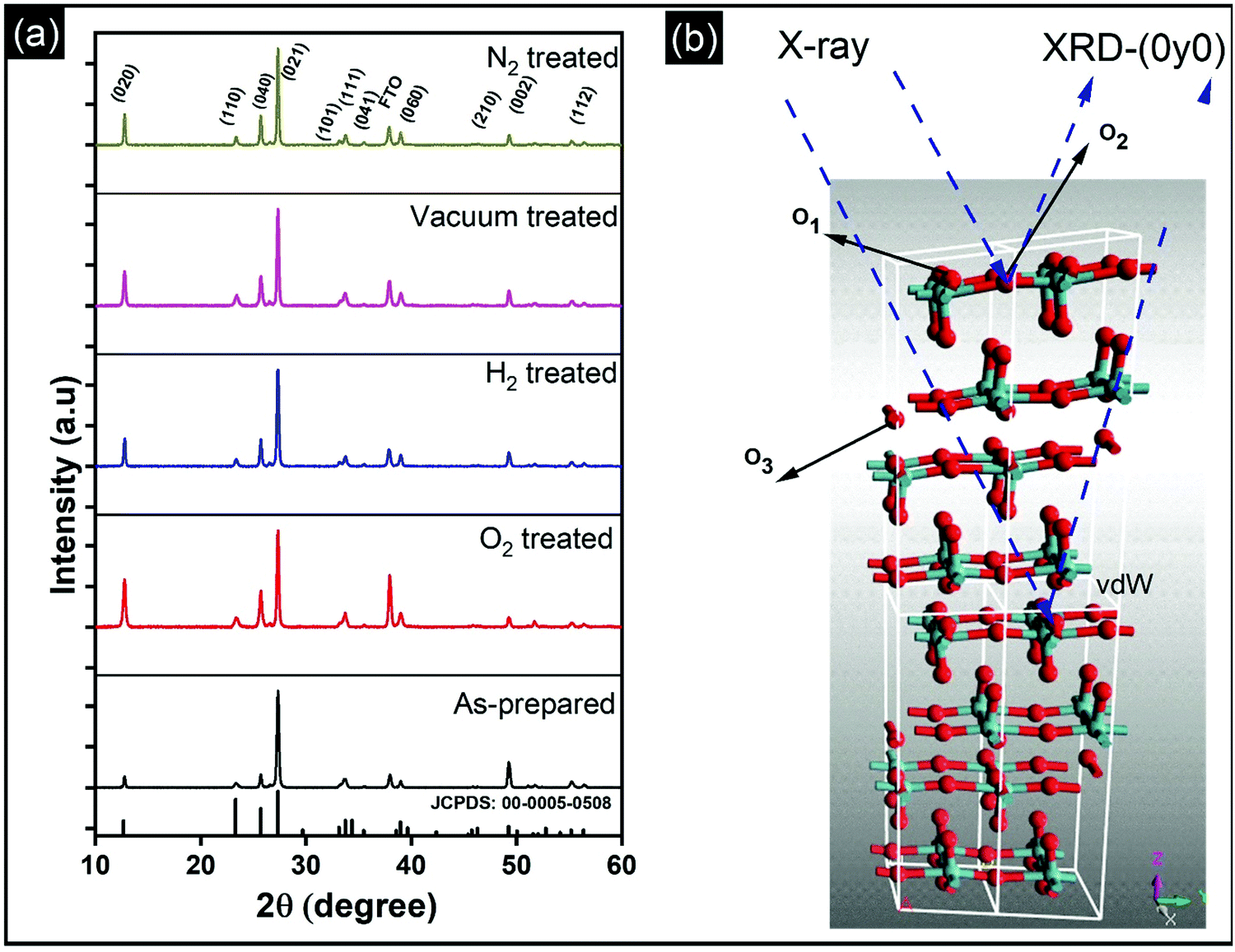 | ||
| Fig. 1 (a) X-Ray diffraction patterns of vertically aligned α-MoO3 on FTO substrates prepared by hydrothermal technique and post-treated at 400 °C for 3 h under different atmospheres such as oxidizing (O2) or reducing (H2, vacuum, N2). (b) Illustration of the crystal structure of the vertically aligned α-MoO3 nanoblades grown in z-direction with indication of the stacked layers via van der Waals (vdW) bonds in the y-plane and its oxygen atom positions in the crystal as O1, O2, O3 in apical, corner sharing and edge sharing in the octahedra, respectively. The dashed blue lines illustrate the incident X-ray beam on the substrates on the direction of the vdW bonds. | ||
The diffraction patterns of the α-MoO3 nanoblades treated at 400 °C under oxidizing and reducing atmospheres show the material to be highly crystalline; there were no peak shifts observed relative to the patterns of as-prepared films. However, we note that the peak intensities were significantly dependent on the treatment conditions. The origin of such a variation in the XRD peak intensity has been attributed in the literature to the change in the preferred crystal orientation, stoichiometry, and defects. A change of crystal orientation normally occurs due to the change in the synthesis process which is not applicable in our case.22,23Table 1 summarizes the change in the relative intensity of the XRD diffraction peaks, which is calculated with respect to the (021) diffraction peak. Interestingly, the relative intensities increase in (0k0) reciprocal planes with k = 2,4,6. This reflects an increase in the number of scattering centers, which causes a more pronounced amplitude of the scattered intensity in that plane and suggests that none of the vacancies are introduced in the y-plane (van-der-Waals gap) (O1 lattice site; see Fig. 1b). In contrast, the relative intensities in the (002) plane decrease, which suggests a decrease in the scattering centers (atoms, O3 lattice site) in that plane. The increase in the number of scattering centers in the y-direction is consistent with the work of Duo et al., which suggests that rearrangement and refilling of the vacancies spontaneously happens in the y-direction,24 affirming our understanding of the existence of the vacancies in the (x, z) plane.
| Plane | Relative intensity with respect to (021) peak (%) | ||||
|---|---|---|---|---|---|
| As-prepared | O2 | H2 | Vacuum | N2 | |
| (021) | 100 | 100 | 100 | 100 | 100 |
| (020) | 11 | 49 | 29 | 35 | 31 |
| (110) | 4 | 9 | 7 | 11 | 8 |
| (040) | 14 | 38 | 28 | 29 | 30 |
| (111) | 9 | 14 | 10 | 13 | 10 |
| (060) | 7 | 14 | 11 | 13 | 13 |
| (002) | 26 | 10 | 14 | 14 | 10 |
The increase in the peak intensity suggests an improved crystallinity under all conditions. According to vdW-DFT calculations by Inzani et al., the oxygen vacancies in the O1 and O3 lattice sites cause less lattice distortion in comparison to the O2 site where the highest lattice distortion can occur.17 The DFT + revised Perdew–Burke–Ernzerhof (RPBE) calculations by R. Tokarz further indicate that the O1 site (y-plane) has the largest formation energy in comparison to oxygen defects in the O2 and O3 sites.25 This implies that the oxygen vacancies in the O2 and O3 sites allow polaron migration (T > 20 K) and replenishment of vacancies in the O1 sites. The polaron migration can occur by charges hopping between nonequivalent Mo6+ sites (i, j), which assess the existence of Mo5+ and related oxygen vacancy, as given by the relation26
 | (1) |
To gain further insights into vacancy formation and to validate the XRD data, we performed high resolution transmission electron microscopy (HR-TEM) and recorded selected area electron diffraction (SAED) patterns of the α-MoO3 nanoblades. SAED has been used to define dislocations and deformations in the diffracted lattice points (corresponding to the lattice spacing d) in the x- and z-planes (Fig. 2). The surfaces of all post-treated α-MoO3 nanoblades show random spots of lower contrast after the heat treatment for all conditions. The SAED patterns show no deviation from the initial degree of crystallinity after various treatments, as also confirmed by XRD data. Additionally, the SAED patterns reflect the diffraction patterns corresponding to the zone axis of [x0z]. This allows us to calculate the inter-planar spacing (d-spacing) in those planes (d = 2/reciprocal lattice). The d-spacing values (Table 2) remain nearly unchanged in one direction and are in good agreement with the standard lattice constant a = 0.396 nm (x-direction). In the z-direction, the d-spacing values, however, vary significantly from the standard (lattice constant c = 0.369 nm). The d-spacing value for the O2-treated sample shows the best match with the standard value, suggesting that oxygen treatment tends to produce highly defect-free nanoblades. The d-spacing values for the reduced α-MoO3 samples show a higher deviation from the standard value. The vacuum treated samples show a smaller deviation, while the H2 and N2 treated samples show the highest deviations.
 | ||
| Fig. 2 (a–e) HR-TEM micrographs and SAED patterns of as-prepared α-MoO3 nanoblade and treated nanoblades under O2, H2, vacuum and N2 conditions, respectively with the measured d-spacings. | ||
| Samples | Lattice-spacing (nm) | |
|---|---|---|
| dc | da | |
| As-prepared | 0.38 | 0.40 |
| O2 | 0.37 | 0.39 |
| H2 | 0.34 | 0.38 |
| Vacuum | 0.37 | 0.38 |
| N2 | 0.34 | 0.39 |
These results suggest that the oxygen vacancies are introduced into the crystal upon thermal post-treatment. According to vdW-DFT calculations, the formation of oxygen vacancies in the z, x-plane leads to less perturbation (not exceeding ≈0.02 nm) in the positions of Mo ions toward the closest O ions in comparison to y-plane oxygen vacancies.18 This closely matches the d-spacing values of O2 and vacuum-treated samples. In the case of H2 and N2 treated samples, however, we note a deviation >0.02 nm. We attribute this to substitution of the oxygen atom for the adsorbed H and N, which can be assumed as an external doping (defect), respectively. The substitution of an oxygen atom (atomic radius 0.48 Å27i) with the larger atomic H and N atoms (atomic radii 0.53 and 0.56 Å, respectively) can be the cause of the additional shrinking of the d-spacing, as a relatively small increase of the cell volume and slight distortion of the lattice,8 see Table 2.
We further employed electron paramagnetic resonance (EPR), which is a sensitive tool for detecting a minor concentration of shear structures, point defects, reduced ions, oxygen radical species, and colour centers.28Fig. 3a shows the continuous wave (CW) EPR spectra recorded at 80 K of as-prepared α-MoO3 nanoblades and of α-MoO3 nanoblades treated under oxidizing and reducing atmospheres. The signal intensity is plotted as a function of the g values. This allows for a direct comparison of the EPR spectra irrespective of slight variations of the microwave frequency from one measurement to the other. The g-values have been calculated according to the following equation:29
 | (2) |
 | ||
| Fig. 3 (a and b) EPR spectra of as-prepared α-MoO3 nanoblades and treated nanoblades under O2, H2, vacuum and N2 atmospheres. (c) The integrated intensity versus α-MoO3 nanoblades treatment condition. | ||
In oxidized α-MoO3 nanoblades a low intensity signal has been recorded, which is at the same position of the original signal of α-MoO3. This signal can be attributed to a very low concentration of Mo5+ ions and the existence of weakly bound F-centers. The F-centers have been assumed to exist as metal cations in two different oxidation states (6+ and 5+), where the free electron (stemming from oxygen vacancies) can be trapped into other cation sites. Pick et al. have shown the existence of two types of F-centers, which differ in how strongly the electron is bound to the defect site. The weakly bound centers can be ionized and bleached at low temperatures with a broad absorption band.36,37 The more strongly bound F-center requires a higher temperature to be ionized and provides electrons to the weakly bounded F-center as a bound excited state.38 The spectrum of vacuum treated nanoblades exhibits an asymmetric line shape, which is attributed to the local crystal field with nonaxial symmetry and a pronounced hyperfine structure, in agreement with previous studies.28,30–32 However, in the N2 treated nanoblades the hyperfine structure cannot be observed. The H2 treated nanoblades show the same broadening as the ones treated with N2, with a hyperfine structure related to g-tensors that fits well with previous reports on the effect of H+ on the MoO6 octahedral structure. Untreated and reduces α-MoO3 nanoblades g-tensors are found to be 1.956 and 1.946, respectively, and reflect Mo5+ species which can be explained by structural changes.39 Various previous EPR studies of Mo5+ species assigned that signal to hexacoordinated Mo(V) centers in shear defects caused by an off-center shift of the Mo atom towards a surrounding oxygen.30,40 Those results suggest a rearrangement of the vacancies from corner to edge sharing (x- to z-) planes, in agreement with the finding of a decrease in the relative intensity of the z-plane in XRD patterns. Additionally, the spin Hamiltonian function which has been given by K. Dyrek et al., indicates a weakening of the octahedral crystal field around Mo5+, which confirms a strong lattice distortion in that plane.30 A hydrogen rich atmosphere is found to reduce Mo6+ and result in full occupancy of the anionic sites addressed to the (MoO6)7− cluster of octahedral Mo5+. A N2 rich atmosphere can accept one electron from the oxygen in the crystal and result in N2− (not paramagnetic active impurities), which allows detection of stabilized radical O˙− in shear structures along the x, z-plane.28,32 The lower intensity of the vacuum treated sample spectrum confirms the lower concentration of free radical ions, which can lead to a difference in the electrical conductivities between N2, H2 and vacuum treated samples. It is essential to indicate that Mo4+ (MoO2) can be formed in both cases of rich H+ and high-temperature vacuum treated conditions (have not been detected by XRD) or even Mo3+ (not sensitive to EPR). For oxidized MoO3 nanoblades, the EPR signal for the radical O2− stabilized in Mo6+ was not detected in our case, which suggests the higher stability of our structure (ex situ nanoblades).
Using XRD, SAED, and EPR we have verified that oxygen vacancies have been eliminated from corner to edge-sharing α-MoO3 nanoblades (x-, z-planes). A quantity of Mo5+ ions in each sample was determined from the comparison with the EPR intensity of a standard CuSO4 sample as an indication of substoichiometric effects. Under the assumption that only Mo5+ species contribute to the EPR intensity and that there is an oxygen vacancy corresponding to each Mo5+ ion, the stoichiometry of the α-MoO3-based materials was evaluated in Table 3. To identify the paramagnetic species/defects in the oxidized and reduced α-MoO3 nanoblades, we undertook spectral simulations (ESI† Fig. S2). Due to the broad EPR spectra that lack any resolved fine structure, the characteristic g-values of individual Mo5+ species cannot be extracted from the spectrum. Instead, a set of known g-values was used, which corresponds to various individual Mo5+ species as they have been determined in reduced α-MoO3 nanoblades.
| Sample | Stoichiometry |
|---|---|
| As-prepared | MoO2.994 |
| O2 treated | MoO3.000 |
| H2 treated | MoO2.951 |
| Vacuum treated | MoO2.996 |
| N2 treated | MoO2.957 |
Electrical characterization of α-MoO3 nanoblades
To measure the electronic properties, vertical α-MoO3 nanoblade films have been connected between two metal electrodes as a bottom-top electrode configuration. Fig. 4a shows the FE-SEM top micrograph of evaporated Au on the vertically aligned α-MoO3 nanoblades on FTO substrates. Room temperature current–voltage (I–V) characteristic curves of as-prepared and thermally treated Au/MoO3 nanoblades on FTO substrates are shown in Fig. 4b.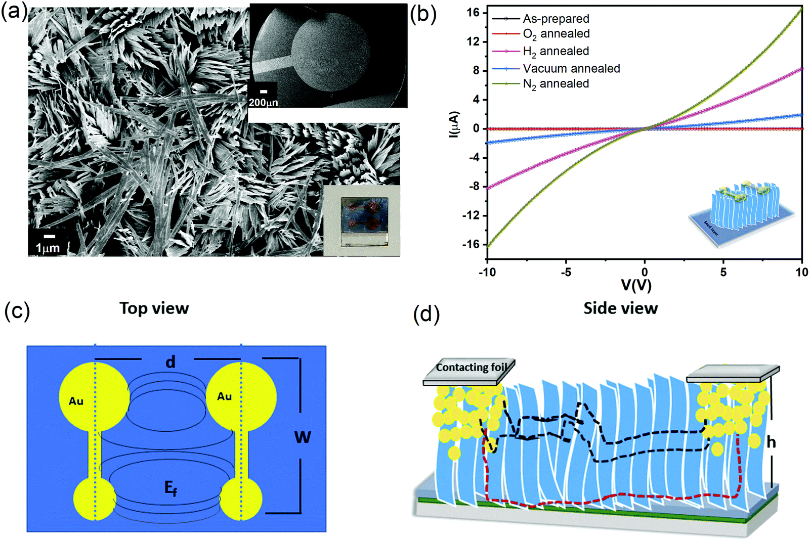 | ||
| Fig. 4 (a) FE-SEM micrograph of evaporated Au on the vertically aligned α-MoO3 nanoblades; the inset is a schematic resembling a final electrical device. (b) Room temperature I–V curves of as-prepared post-treated α-MoO3 nanoblade based devices. (c) Top view of the evaporated co-planar Au electrodes (d is the distance between the two central points of the electrodes terminals, W is the length of the electrode, Ef is a schematic of the supposed electrical field). (d) Side view of the electrical device (h is the nanoblade length) with illustration of possible electrical pathways through the devices. The red dashed line represents charge flow through the nanoblades and the seed layer, and the black dashed line represents the path through interconnected nanoblades. | ||
The electric field through such an electrode structure is not uniform (see Fig. 4c). These electrodes, however, offer a higher current sensitivity in comparison to conventional rectangular electrodes.41 In addition, it has been demonstrated that the narrow gap between the electrode terminals leads to a lateral current flow. This is different from the conventional co-planar electrodes (with a larger inter-electrode gap), where a lateral and horizontal current flow is likely (perpendicular to the substrates) (Fig. 4d).42 In our electrode setup, the current can flow along two possible pathways, directly to the second terminal electrode via interconnected nanoblades or via the seed layer (see Fig. 4d). The seed layer shows a nearly insulating behaviour at room temperature (Fig. S3a, ESI†), consistent with previous reports on the air treated α-MoO3 as the insulator layer.43,44
We recorded temperature dependent I–V characteristics of α-MoO3 devices (Fig. S4a–e, ESI†). The semi-logarithmic temperature dependent I–V curves show nonlinearity and symmetric trends at both forward and reverse biasing conditions. This behavior suggests the formation of a negligible Schottky barrier at the interfaces between the metal electrode and the nanoblades (Au/α-MoO3/Au diode).45,46 The non-linearity in the I–V characteristics suggests the formation of the barrier at the interfaces between the electrodes and the metal oxide.45 The conduction mechanism shows Ohmic conduction (0–3 V), which is categorized as a bulk limited conduction mechanism. Such a conduction mechanism shows dependence on the intrinsic semiconductor properties resulting from the movements of mobile electrons in the conduction bands and holes in the valence band.47 The electrical conductivity (σ) has been calculated in the Ohmic region using the following relation:47
 | (3) |
The activation energy EA can be deduced from the Arrhenius law as follows:
 | (4) |
| Sample | Conductivity (Sm−1) | E A1 (eV) | E hopping (eV) |
|---|---|---|---|
| As-prepared | (6.04 ± 2.85) × 10−6 | 0.34 ± 0.02 | 0.38 ± 0.05 |
| O2 treated | (3.67 ± 0.90) × 10−4 | 0.38 ± 0.02 | 0.41 ± 0.02 |
| H2 treated | (9![[thin space (1/6-em)]](https://www.rsc.org/images/entities/char_2009.gif) .95 ± 2.57) × 10−2 .95 ± 2.57) × 10−2 |
0.23 ± 0.01 | 0.24 ± 0.02 |
| Vacuum treated | (2.60 ± 0.33) × 10−2 | 0.26 ± 0.01 | 0.29 ± 0.00 |
| N2 treated | (12.80 ± 1.79) × 10−2 | 0.28 ± 0.01 | 0.30 ± 0.01 |
Our vertically aligned α-MoO3 films show significantly higher electrical conductivity in comparison to previous studies on similar nanostructured films based on α-MoO3.17,50 The N2, H2 and vacuum treated samples show a higher conductivity than their as-prepared counterparts. As expected, O2 treated nanoblades show a reduced conductivity, which confirms a re-adsorption and restitution of oxygen into the crystal. It is important to note that due to their highest conductivity, the N2 treated samples show a sudden decrease in the current at high temperature (Fig. S4e, ESI†), which can be attributed to damage or deformation in the structures. The high conductivities can be attributed to different factors: the higher density of the interconnected nanoblades grown on the substrate facilitate the carrier transport,17 a high surface to volume ratio of the very thin sheet-like structures, and the crystalline nature of the nanoblades.17
The calculated values of EA (Table 4) for the reduced and oxidized vertically aligned α-MoO3 nanoblades imply the existence of shallow levels close to the conduction band minimum. These values match the previously reported theoretical and experimental values in the literature.14 The vdW-DFT calculations17 showed the transition energies of the three different oxygen vacancy positions to the valence band maximum to follow the order O1 < O3 < O2 (see Fig. 1b for O positions in the crystal). The O1 vacancy constitutes the deepest intra-band level, whereas the O2 vacancy marks the shallowest defect state, as indicated in a recent study by Inzani et al.14 A further study by Ding et al.18 on the localized electron small polarons (refers to Mo5+) in α-MoO3, revealed polaron migration and hopping to neighboring Mo sites in the same plane. Ding et al. highlighted anisotropy in the activation energy and hopping paths and distances within the same plane of the bilayer, zigzag in comparison to transition across the van der Waals gap. The lowest activation energy and fast polaron migration was found to be in the same plane of the bilayer sheet (corresponding to O2, O3 in the (x, z) plane).18 As previously demonstrated studies about the color center formation in MoO3, it can be explained via small polaron theory.18,51 The first investigation by Mott in 196852 affirms that small polaron hopping occurs when thermal energies are coinciding with the closer energy level of nearby atoms, which contribute at the transition between different metal oxidation states.53 The conductivity is attributed to the movement of the electron between various cation sites, which suggests a hopping mechanism.52
The hopping activation energy Ehopping can be determined through the following eqn (3):52
 | (5) |
 | ||
| Fig. 5 Arrhenius plot on the Ohmic region of the applied voltage (0–3 V) with schematic illustrating the corresponding activation energy in the band diagram. The inset figure shows the Arrhenius plot corresponding to the hopping mechanism in the same region of the applied voltage. | ||
Optical characterization of α-MoO3 nanoblades
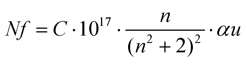
In order to investigate the role of oxygen vacancies in the color center formation, we performed diffuse reflectance spectroscopy (DRS). DRS can provide information about the dispersion and optical constants. DRS is considered as a reliable measurement for such film surfaces where multiple reflections and diffusion of the incident waves are likely to occur (porous-like surface of the vertical nanoblades). Recently, Kumar et al.54 measured various thick films using the diffuse reflectance to estimate the optical band gap using the relation55,56 | (6) |
| α(hν)ph = k(hν − Eg ± Ep)1/n | (7) |
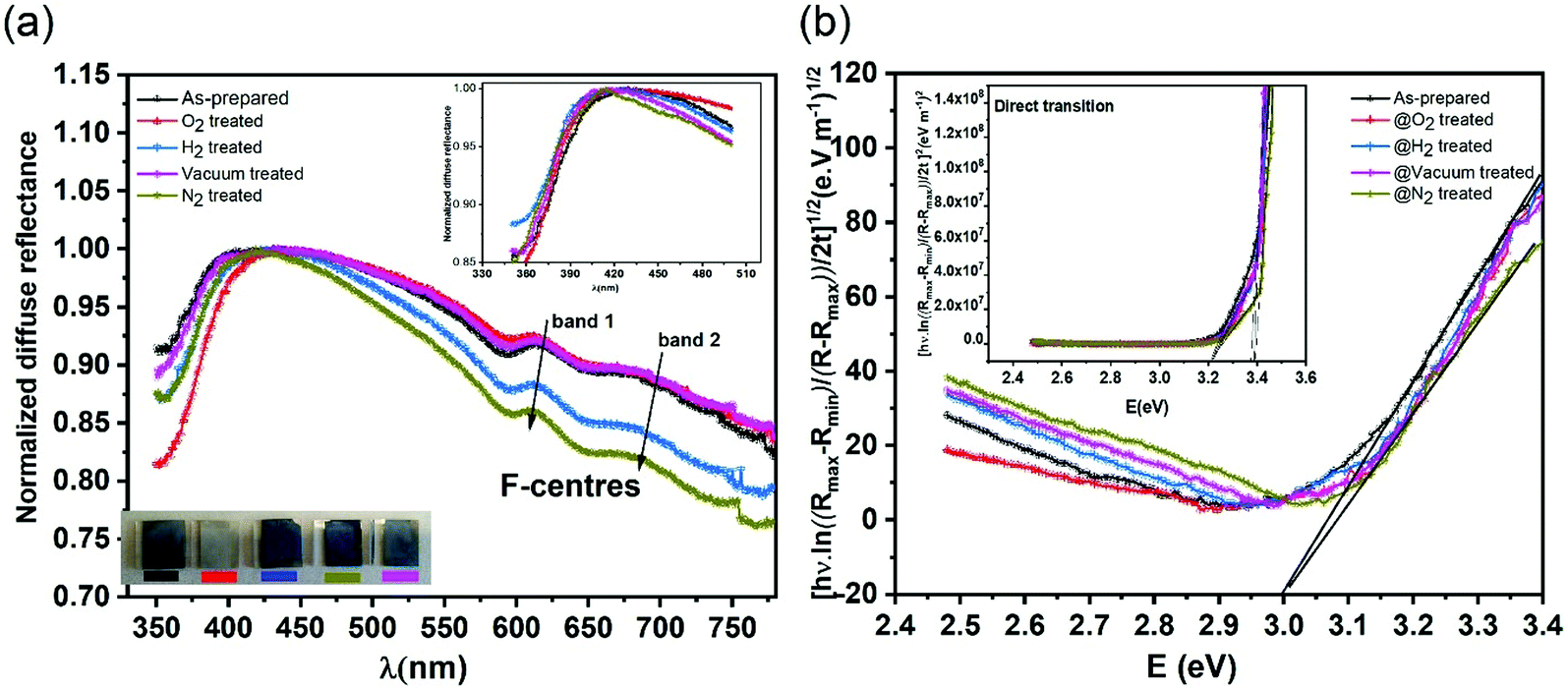 | ||
| Fig. 6 (a) Diffuse reflectance spectra of vertically aligned α-MoO3 on FTO substrates as-prepared and treated under O2, H2, vacuum and N2 atmosphere, the inset figure shows the optical bandgap position. (b) Direct and indirect transitions subtracted from diffuse reflectance spectra. | ||
Fig. 6b shows the allowed direct and indirect transitions. The lowest energy transition occurs as an indirect transition with an energy of 3.00 ± 0.05 eV, and the direct transition happens at a slightly higher energy of 3.20 ± 0.05 eV. This shows exciton absorption at an energy of ≈0.20 eV. We do not observe any significant change in the optical band gap; however, there is a minor change in the position of the color center bands and small variations between the concentrations of the color center under different reducing atmospheres in comparison to treatment under a rich O2 atmosphere which shows the lowest density. The color center density N (cm−3) can be estimated through Smakula's equation:60
 | (8) |
Conclusions
Vertically aligned α-MoO3 nanoblades have been introduced into oxidizing and reducing atmospheres at a temperature of 400 °C to tune their oxygen vacancy concentrations. Our results demonstrate a fundamental experimental approach for the formation of oxygen vacancies within the bilayer of the crystal structure, which is consistent with previously reported theoretical and computational studies. The amount of the oxygen deficiencies in α-MoO3 nanoblades as a result of the post-treatment under oxidizing and reducing atmospheres has been evaluated using EPR. The electronic properties have been studied using top co-planar electrodes. The material shows n-type behavior under reducing atmospheres and degenerated n-type behavior under an oxidizing atmosphere. This has been explained using color-center formation models and polaron migration. The electrical conductivity is found to be altered in the change from 7 × 10⁻⁶ to 1 × 10⁻² Sm−1 for oxidized to reduced α-MoO3 nanoblades, respectively, which showed higher conductivity compared to previously reported values for similar morphologies. The obtained highly conductive MoO3 nanoblade film is favorable for high charge mobility in the next generation of electronics and in new generation batteries.Methods
Synthesis procedure and post-treatments
Laterally grown α-MoO3 nano-blades have been synthesized directly on seeded fluorine doped tin oxide substrates (FTO) (15 Ω cm−2), via the hydrothermal technique.20 Briefly, 14 × 14 mm FTO substrates were subjected to a standard cleaning procedure by sonication for 5 min in acetone and isopropanol each, followed by sonication in ethanol for 15 min and drying in a nitrogen flow. The cleaned substrates were treated with UV/ozone (Ossila) for 20 min. The seed layer was deposited on the substrates consecutively from two evaporation sources: chrome plated tungsten rods (99.9%) (Testbourne) and molybdenum(VI) oxide (99.98%) powder (Sigma Aldrich) using thermal evaporation (Tectra mini-coater) at a base pressure of <2 × 10⁻⁶ mbar with an applied current and power of 15 A and 1 kW, respectively. The thickness of the seed layer was 5 nm/100 nm for Cr/MoO3 and was monitored by a quartz micro-balance with a resolution of ± 0.1 nm. Finally, the seed layer coated substrates were annealed at 450 °C for 1 h in an ambient atmosphere. An aqueous solution of Na2MoO4·2H2O (99.5%) (Sigma Aldrich) has been prepared in a PTFE autoclave liner to yield a total volume of 21.5 ml and a concentration of 0.1 M. 0.29 mol L−1 hydrochloric acid (HCl) (37% VWR chemicals) was added dropwise to the solution under continuous stirring for 10 min. Then, the seed layer coated substrates were inserted upright into a PTFE holder in the precursor solution. Finally, the PTFE autoclave liner was sealed and put into a pre-heated oven at 180 °C for 210 min. After the reaction, the autoclave was rapidly cooled down to ambient temperature in a water bath. The substrates of the vertically aligned α-MoO3 nanoblades were washed with ethanol and allowed to dry under ambient conditions. The substrates are annealed separately for 3 h at 400 °C with a heating rate of 10 °C min−1 in a digital controlled oven under different atmospheres, O2, N2 and H2 (500 sccm) and under vacuum conditions.Characterization techniques
Surface imaging was done using a Zeiss Cross Beam 1540XB field emission SEM using an acceleration voltage of 5 kV. X-Ray diffraction analysis XRD was performed using a Bruker AXS D8 Advance diffractometer employing a Bragg–Brentano geometry and Cu-Kα radiation. High resolution transmission electron microscopy (HR-TEM) images were obtained on a JEOL-2010 microscope operated at 200 kV. The TEM samples were prepared on holey carbon films Multi A TEM grids supplied by Quantifoil GmbH. Zero-loss filtered bright-field images and selected area electron diffraction (SAED) patterns were recorded. Using electron paramagnetic spectroscopy (EPR), spectra were recorded as follows: powder α-MoO3 nanoblades were prepared using sonication of the vertically aligned grown α-MoO3 nanoblades on the substrates in DI water for 3 min. The powder was purified using centrifugation under 9000 rmp for 20 min. The obtained powder was divided to be annealed under different atmospheric conditions separately, as mentioned before for the substrates. Continuous-wave (cw) EPR spectra were recorded at the X-band (∼9.3 GHz) on an Elexsys E580 EPR spectrometer (Bruker Biospin) equipped with a split-ring resonator ER 4118X-MS3 (Bruker Biospin). The measurements were performed at 80 K, which was realized in a gas-flow cryostat CF935O combined with a temperature controller ITC503 (both from Oxford Instruments) and using helium as a cooling agent. Experimental settings were adjusted to avoid any saturation and over modulation of the spectral lines. Typical experimental settings were: modulation amplitude of 1 G, modulation frequency of 100 kHz, microwave power of 0.64 mW, magnetic field range of 1000 G, time constant of 40.96 ms, conversion time of 40.96 ms, number of points per scan 4096, and number of scans 4. All samples were measured in 3 mm/2 mm (o.d./i.d.) quartz tubes (Technical Glass Products, Inc.). As prepared and treated α-MoO3 nanoblades were placed as a powder and pressed slightly with a plastic piston from the top to avoid any occasional movement of the powder particles in the magnetic field. The weight of the powder sample was determined as a difference in masses of the empty quartz tube and the filled ones. The height of all samples in the quartz tubes was approx. 1 cm, which corresponds to the length of the sensitive part of the resonator. The standard CuSO4 sample was prepared from CuSO4·5H2O as a 10 mM solution in a H2O/glycerol (8:2 v/v) mixture; 30 μL of this solution was transferred into a quartz tube and shock frozen in liquid nitrogen prior to the measurement. Spectral simulations were performed with the EasySpin software package for Matlab.61 The X-ray photoelectron spectroscopy XPS measurements were performed in ultrahigh vacuum (UHV) using standard Omicron XPS system with a Mg X-ray source. The samples were exposed to air before inserting into the UHV system. CASA XPS software was used for the fitting of the data. C 1s was used as a reference for the calibration of the data. Photoelectron spectroscopy in air (PESA) measurements has been carried out on an AC-2 instrument (Riken Instruments). The analysis has been performed at an excitation light power of 2400 nW and scanned from 4.6 eV to 6.2 eV with a step size of 0.05 eV. The measurements have been recorded for three different positions on the substrate and repeated three times for each position. Temperature-dependent current–voltage characteristics have been measured using a home-made DC chamber, with an embedded ceramic heat element (SiNi type CLV) connected to a digital temperature controller TR400 with a CX-Thermo OMRON E58-CIFQ2. The temperature is adjusted digitally through a Pt-100 thermocouple that is fastened to the top of the substrates and connected to the temperature controller. The samples are measured in the temperature range of 30–130 °C with steps of 10 °C in 30 s and stabilization time of 5 min. Purpose-built current–voltage contacting probes were made of Ni foil covered with an evaporated thin layer of Cr as adhesion layer followed by a 150 nm thick Au layer (to reduce the resistance between the probes and our top electrodes on the vertically aligned α-MoO3 nanoblades). As an extreme precaution, a Ni foil was used to make sure that the vertically aligned nanoblades are not destroyed by the weight of the contacting probes. A Keithley 2400 source meter was connected to the contacting probes and the data acquisition was controlled by a Matlab program. Two Au top electrodes of 120 nm thickness were directly evaporated through a mask onto grown and treated vertically aligned α-MoO3 nanoblades. Diffuse reflectance spectra were recorded by a Cary5000 (Agilent technologies) from 400 to 800 nm in a 150 mm integrating sphere. The samples were housed in the back of integrated sphere where the incident light illuminates the samples perpendicularly.
Conflicts of interest
There are no conflicts to declare.Acknowledgements
The authors sincerely acknowledge the German Academic Exchange Service (DAAD) and the Egyptian Ministry of Higher Education (General Administration of Mission) for funding the reported work. The work was supported by the Deutsche Forschungsgemeinschaft (DFG) through the Collaborative Research Center SFB 1214 project Z1 (Particle Analysis Center). The authors are grateful to Mr Tobias Seewald (Physics department, University of Konstanz) for his professional and precise revision of the article.References
- S. Tokito, K. Noda and Y. Taga, J. Phys. D: Appl. Phys., 1996, 29, 2750–2753 CrossRef CAS.
- J. Meyer, K. Zilberberg, T. Riedl and A. Kahn, J. Appl. Phys., 2011, 110, 033710 CrossRef.
- K. Kanai, K. Koizumi, S. Ouchi, Y. Tsukamoto, K. Sakanoue, Y. Ouchi and K. Seki, Org. Electron., 2010, 11, 188–194 CrossRef CAS.
- P. A. Spevack and N. S. Mcintyre, J. Phys. Chem., 1992, 96, 9029–9035 CrossRef CAS.
- M. T. Greiner, L. Chai, M. G. Helander, W.-M. Tang and Z.-H. Lu, Adv. Funct. Mater., 2013, 23, 215–226 CrossRef CAS.
- W. Gordy and W. J. O. Thomas, J. Chem. Phys., 1956, 24, 439–444 CrossRef CAS.
- E. D. Hanson, L. Lajaunie, S. Hao, B. D. Myers, F. Shi, A. A. Murthy, C. Wolverton, R. Arenal and V. P. Dravid, Adv. Funct. Mater., 2017, 27, 1605380 CrossRef.
- A. Borgschulte, O. Sambalova, R. Delmelle, S. Jenatsch, R. Hany and F. Nuesch, Sci. Rep., 2017, 7, 40761 CrossRef CAS PubMed.
- M. T. Greiner, L. Chai, M. G. Helander, W. M. Tang and Z. H. Lu, Adv. Funct. Mater., 2012, 22, 4557–4568 CrossRef CAS.
- T. He and J. Yao, J. Photochem. Photobiol., C, 2003, 4, 125–143 CrossRef CAS.
- N. Li, Y. Li, W. Li, S. Ji and P. Jin, J. Phys. Chem. C, 2016, 120, 3341–3349 CrossRef CAS.
- S. Subbarayudu, V. Madhavi and S. Uthanna, ISRN Condens. Matter Phys., 2013, 2013, 1–9 CrossRef.
- P. R. Huang, Y. He, C. Cao and Z. H. Lu, Sci. Rep., 2014, 4, 7131 CrossRef CAS PubMed.
- K. Inzani, T. Grande, F. Vullum-Bruer and S. M. Selbach, J. Phys. Chem. C, 2016, 120, 8959–8968 CrossRef CAS.
- Y. Li, X. Chen, M. Zhang, Y. Zhu, W. Ren, Z. Mei, M. Gu and F. Pan, Catal. Sci. Technol., 2019, 9, 803–810 RSC.
- R. Kashfi-Sadabad, S. Yazdani, T. D. Huan, Z. Cai and M. T. Pettes, J. Phys. Chem. C, 2018, 122, 18212–18222 CrossRef CAS.
- K. Inzani, M. Nematollahi, F. Vullum-Bruer, T. Grande, T. W. Reenaas and S. M. Selbach, Phys. Chem. Chem. Phys., 2017, 19, 9232–9245 RSC.
- H. Ding, H. Lin, B. Sadigh, F. Zhou, V. Ozoliņš and M. Asta, J. Phys. Chem. C, 2014, 118, 15565–15572 CrossRef CAS.
- Y. Gong, Y. Dong, B. Zhao, R. Yu, S. Hu and Z. A. Tan, J. Mater. Chem. A, 2020, 8, 978–1009 RSC.
- S. Z. Noby, K. K. Wong, A. Ramadoss, S. Siroky, M. Hagner, K. Boldt and L. Schmidt-Mende, RSC Adv., 2020, 10, 24119–24126 RSC.
- International Centre for Diffraction Dat (ICDD).
- A. A. Ramadan, A. A. Abd El-Mongy, A. M. El-Shabiny, A. T. Mater, S. H. Mostafa, E. A. El-Sheheedy and H. M. Hashem, Cryst. Res. Technol., 2009, 44, 111–116 CrossRef CAS.
- D. J. Goyal, C. Agashe, M. G. Takwale and V. G. Bhide, J. Cryst. Grow., 1993, 130, 567–570 CrossRef CAS.
- Y. Guo and J. Robertson, Appl. Phys. Lett., 2014, 105 Search PubMed.
- K. H. R. Tokarz-Sobieraj, M. Witko, A. Blume, G. Mestl and R. Schlögl, Surf. Sci., 2001, 489, 107–125 CrossRef.
- C. G. Granqvist, in Handbook of Inorganic Electrochromic Materials, ed. C. G. Granqvist, Elsevier Science B. V., Amsterdam, 1995 DOI:10.1016/B978-044489930-9/50010-6, pp. 175–192.
- Journal, 2007.
- M. Labanowska, Phys. Chem. Chem. Phys., 1999, 1, 5385–5392 RSC.
- Comments Inorg. Chem., 1984, 35, 230–238 DOI:10.1080/02603598408080073.
- K. Dyrek and M. Labanowska, J. Chem. Soc., Faraday Trans., 1991, 87, 1003–1009 RSC.
- A. Varlec, D. Arčon, S. D. Škapin and M. Remškar, Mater. Chem. Phys., 2016, 170, 154–161 CrossRef CAS.
- E. Serwicka, J. Solid State Chem., 1984, 51, 300–306 CrossRef CAS.
- K. C. Radha, R. V. Anavekar, J. L. Rao and R. P. S. Chakradhar, Appl. Magn. Reson., 2008, 35, 1–13 CrossRef CAS.
- X.-S. Jia, C.-C. Tang, X. Yan, G.-F. Yu, J.-T. Li, H.-D. Zhang, J.-J. Li, C.-Z. Gu and Y.-Z. Long, J. Nanomater., 2016, 2016, 9102828 Search PubMed.
- N. S. Kopachevska, A. K. Melnyk, I. V. Bacherikova, V. A. Zazhigalov and K. Wieczorek-Ciurowa, Himia, Fizika ta Tehnologia Poverhni, 2015, 6, 474–480 CrossRef.
- H. Pick, Ann. Phys., 1938, 423, 365–376 CrossRef.
- H. Pick, Ann. Phys., 1940, 37, 421–428 CrossRef CAS.
- D. A. R. D. W. Lynch, Phys. Rev., 1968, 174, 1050–1059 CrossRef CAS.
- S. S. Sunu, E. Prabhu, V. Jayaraman, K. I. Gnanasekar, T. K. Seshagiri and T. Gnanasekaran, Sens. Actuators, B, 2004, 101, 161–174 CrossRef CAS.
- E. S. E. Haber, Polyhedrton, 1986, 2, 107–109 CrossRef.
- C. Clausen, G. Skands, C. Bertelsen and W. Svendsen, Micromachines, 2014, 6, 110–120 CrossRef.
- M. J. Toohey, Sens. Actuators, B, 2005, 105, 232–250 CrossRef CAS.
- C. Julien, A. Khelfa, O. M. Hussain and G. A. Nazri, J. Cryst. Growth, 1995, 156, 235–244 CrossRef CAS.
- V. Nirupama, K. R. Gunasekhar, B. Sreedhar and S. Uthanna, Curr. Appl. Phys., 2010, 10, 272–278 CrossRef.
- R. K. Gupta, K. Ghosh and P. K. Kahol, Phys. E, 2010, 42, 1509–1512 CrossRef CAS.
- H. M. Chenari, H. Sedghi, M. Talebian, M. M. Golzan and A. Hassanzadeh, J. Nanomater., 2011, 2011, 1–4 CrossRef.
- F.-C. Chiu, Adv. Mater. Sci. Eng., 2014, 2014, 1–18 Search PubMed.
- R. Aigner, A. Pointner, T. Preindl, P. Parzer and M. Haller, Presented in part at the Proceedings of the 2020 CHI Conference on Human Factors in Computing Systems, 2020 Search PubMed.
- R. Nigon, T. M. Raeder and P. Muralt, J. Appl. Phys., 2017, 121, 204101 CrossRef.
- J. Yang, X. Xiao, P. Chen, K. Zhu, K. Cheng, K. Ye, G. Wang, D. Cao and J. Yan, Nano Energy, 2019, 58, 455–465 CrossRef CAS.
- H. A. Tahini, X. Tan, S. N. Lou, J. Scott, R. Amal, Y. H. Ng and S. C. Smith, ACS Appl. Mater. Interfaces, 2016, 8, 10911–10917 CrossRef CAS PubMed.
- I. G. Austin and N. F. Mott, Adv. Phys., 1969, 18, 41–102 CrossRef CAS.
- R. A. S. Y. P. Yadava, Mater. Chem. Phys., 1987, 17, 259–272 CrossRef.
- S. K. S. Vipin Kumar, T. P. Sharma and V. Singh, Opt. Mater., 1999, 12, 115–119 CrossRef.
- N. Illyaskutty, S. Sreedhar, G. Sanal Kumar, H. Kohler, M. Schwotzer, C. Natzeck and V. P. M. Pillai, Nanoscale, 2014, 6, 13882–13894 RSC.
- M. Nowak, B. Kauch and P. Szperlich, Rev. Sci. Instrum., 2009, 80, 046107 CrossRef CAS PubMed.
- S. K. Deb and J. A. Chopoorian, J. Appl. Phys., 1966, 37, 4818–4825 CrossRef CAS.
- M. R. Tubbs, Phys. Status Solidi A, 1974, 21, 253–260 CrossRef CAS.
- H. Pick, Ann. Phys., 1940, 429, 421–428 CrossRef.
- S. Deb, Philos. Mag., 1973, 27, 801–822 CrossRef CAS.
- S. Stoll and A. Schweiger, J. Magn. Reson., 2006, 178, 42–55 CrossRef CAS PubMed.
Footnote |
| † Electronic supplementary information (ESI) available. See DOI: 10.1039/d1ma00678a |
| This journal is © The Royal Society of Chemistry 2022 |