
 Open Access Article
 This Open Access Article is licensed under a
 Creative Commons Attribution 3.0 Unported Licence
High-k dielectric screen-printed inks for mechanical energy harvesting devices†
Hannah S.
Leese
 *ab,
Miroslav
Tejkl
c,
Laia
Vilar
d,
Leopold
Georgi
e,
Hin Chun
Yau
af,
Noelia
Rubio
a,
Elisenda
Reixach
d,
Jan
Buk
c,
Qixiang
Jiang
g,
Alexander
Bismarck
g,
Robert
Hahn
*h and
Milo S. P.
Shaffer
*a
*ab,
Miroslav
Tejkl
c,
Laia
Vilar
d,
Leopold
Georgi
e,
Hin Chun
Yau
af,
Noelia
Rubio
a,
Elisenda
Reixach
d,
Jan
Buk
c,
Qixiang
Jiang
g,
Alexander
Bismarck
g,
Robert
Hahn
*h and
Milo S. P.
Shaffer
*a
aDepartment of Chemistry, Imperial College London, London, SW7 2AZ, UK. E-mail: h.s.leese@bath.ac.uk; m.shaffer@imperial.ac.uk
bMaterials for Health Lab, Department of Chemical Engineering, University of Bath, Bath, BA2 7AY, UK
cPardam, Roudnice nad Labem, Czech Republic
dEurecat, Centre Tecnològic de Catalunya, Parc Científic TecnoCampus, Mataró, Barcelona, Spain
eTechnische Universität Berlin, TiB4/2-1, Gustav-Meyer-Allee 25, 13355, Berlin, Germany
fBridgeBlack Limited, Hong Kong Science and Technology Park, Hong Kong
gInstitute of Materials Chemistry and Research, University of Vienna, Währinger Strasse 42, A-1090 Vienna, Austria
hFraunhofer IZM, Gustav-Meyer-Allee 25, 13355 Berlin, Germany. E-mail: Robert.Hahn@izm.fraunhofer.de
First published on 8th January 2022
Abstract
There are a range of promising applications for devices that can convert mechanical energy from their local environment into useful electrical energy. Here, mechanical energy harvesting devices have been developed to scavenge low-frequency energy from regular biomotion such as joint movement and heel strike. Specifically, these harvesters exploit novel printed nanocomposite dielectric inks in combination with commercially available conductive elastomers to develop a low cost, high performance embodiment of a variable capacitance mechanism device. The filler of the nanocomposite dielectric ink, consists of high-k dielectric nanoparticles (barium titanate and strontium doped barium titanate) functionalised with poly(methyl methacrylate) to improve the interface with the epoxy matrix. Characterisation by thermogravimetric analysis coupled to mass spectrometry and X-ray photoelectron spectroscopy confirmed the successful covalent grafting of up to ca. 16 wt% poly(methyl methacrylate) onto the dielectric nanoparticle surfaces, with a thickness of approximately 14 nm, measured by transmission electron microscopy. The dielectric inks were screen printed onto copper-polyimide foils, resulting in large area and flexible five to twenty-micron thick films with dielectric constants up to 45. Nanoparticle polymer functionalisation improved the homogeneity and stability of the inks. Using these screen-printed dielectrics with the commercial conductive elastomer, the mechanical energy harvester prototype demonstrated high mechanical cycling stability and low leakage current. It provided a promising power density of 160 μW cm−3, at low frequency (0.5 Hz), over a 1000 cycles, making the device suitable for wearable applications. This type of harvester has two advantages over the state of the art: it is mechanically flexible for integration into wearables and can be produced at low cost with printing methods.
Introduction
Variable capacity or electrostatic energy harvesting is one of several methods to convert mechanical energy directly into electricity. Such devices are intended to power energy autarkic sensors for internet of things applications or wearable electronics.1–4 Electrical energy can be generated if the capacitance is varied as a function of the mechanical load and if the capacitance is charged and discharged at the right moment of the harvesting cycle. There are three main categories of capacitive energy harvesters:1. MEMS harvesters which use silicon plates as capacitor electrodes and change the capacity by varying the plate distance or the degree of overlap.
2. Elastomer harvesters which use a dielectric elastomer membrane covered with flexible electrodes. Deformation of the uniform membrane alters the capacitance. These devices are closely related to dielectric actuators.5
3. Liquid metal harvesters, in which liquid electrodes are forced to wet and de-wet a dielectric layer, changing the effective area of the electrode.
MEMS and elastomer harvesters are restricted to relative permittivity values of 1 and ∼3 respectively, whereas the liquid metal approach can exploit high dielectric constant (k) materials to improve the capacitance and hence the efficiency of the device. Liquid metal electrode harvesters were first demonstrated using mercury,6 and subsequently developed with room temperature liquid metal alloys (Galinstan).7 However, since mercury is toxic and the liquid alloys suffer from oxidation, there is interest in replacing the droplet electrode, with an electrically-conducting elastomer. Coupled with advances in printed electronics, it is now possible to print complex nanocomposite formulations to manufacture reproducible devices for a variety of applications.8–11
Capacitive harvesters have been successfully demonstrated using carbon-particle filled elastomer electrodes and commercial polymer foil dielectric layers.12 Primarily, the process of pressing and releasing the elastomer electrode onto the dielectric surface, changes the capacitance; however, there can also be a triboelectric contribution, which was recently optimized using core–shell liquid metal inclusions within an elastomeric polymer.13 The energy conversion mechanism of an electrostatic transducer is based on physical coupling of the electrical and mechanical domain by an electrostatic force. In order to convert mechanical energy to electrical energy by means of electrostatic transduction, a variation in capacitance is necessary over time.
It is possible, at practical voltages, to increase the energy density of the harvesting devices by increasing k-values, even at a reduced breakdown strength. Consequently, robust, yet cheap, high-k dielectric films need to be developed for flexible mechanical energy harvesting devices. Improved power density and efficiency will be a crucial enabler for many applications including wearable and portable electronics including pacemakers14,15 and wearable functional smart textiles (clothing, shoe soles),16–19 wireless sensor networks and others. For these reasons, printable, scalable, high-k dielectrics are sought, with the potential for low cost, high-throughput and straightforward fabrication. Ferroelectric ceramics (such as barium and strontium titanate) are often utilised as they offer very high dielectric constants,20,21 but they are not easily translated into formulations for flexible electronics as they are generally mechanically brittle and unprintable. On the other hand, polymers can provide mechanical and synthetic flexibility, however, polymers normally have much lower dielectric constants than their ferroelectric ceramic particle counterparts. A popular approach to convert relatively bulky dielectric materials into printable inks necessary for high-throughput and industrial translation, has been to prepare (nano)composites. Ferroelectric ceramics (as the filler) have been combined with polymers (as the matrix) using various loadings and mixing methods to improve the dielectric constant, dielectric loss and electrical breakdown strength of composite films. However, simple blending has proven insufficient to capture the best qualities of both the filler and matrix. In composites, especially in nanocomposites, it is important to optimise the interface between the two materials to improve both processing and properties; eliminating defects associated with agglomeration can improve both mechanical stability and dielectric properties. One approach has been to functionalise the surface of ferroelectric ceramics with a polymer that has a low interfacial energy with the matrix to encourage and increase dispersibility.22–28 Typical polymer matrices have included, poly(methyl methacrylate) (PMMA),29 epoxy resins, poly(3,4-ethylene dioxythiophene) (PEDOT),23 poly (glycidyl methacrylate) (PGMA)30 and polystyrene (PS).24,31 Poly(vinylidene fluoride) (PVDF and its co-polymers) are also popular as, intrinsically, they have a relatively high dielectric constant.26,32–34 Several high dielectric constant polymer composites have been prepared using ceramic nanoparticles, mainly BaTiO3,25,27,28 ZrO222,35 and TiO236 particles. Most studies have used spherical nanoparticles but there has been some interest in nanofiber ferroelectric ceramics as the high-k fillers.35,37 In addition to nanofiller geometric effects,38 the elemental compositions of the ferroelectric ceramics (e.g. ABX3) can be adjusted to control the dielectric response with temperature.21,39–41 In this work, we have developed a nanocomposite system by combining polymer functionalised nanoparticle and nanofiber perovskite particles, to produce epoxy-based inks for screen printing polymer nanocomposite dielectric films. These films were incorporated into stable mechanical energy harvesting devices by utilising an insulating elastomeric spring element and conductive elastomer (in place of the liquid metal electrode) to enable maximum wetting and de-wetting of the dielectric surface for maximum electrostatic transduction.
Results and discussion
Polymer functionalised nanoparticles
Raw materials of commercial barium titanate (BTO-s) nanoparticles and custom-made strontium doped barium titanate (BSTO-f) nanofibers (provided by Pardam®) were characterised by scanning electron microscopy (SEM) and X-ray diffraction (XRD). The average BTO-s particle diameter was 100 nm (Fig. S1a and b, ESI†) and the BSTO-f particles had an average fibre diameter and length of 200 nm and 10 μm, respectively (Fig. S1c and d, ESI†). The X-ray diffractograms show a definite shift between the BTO and BSTO (Fig. S2, ESI†). Based on Vegard's law, the XRD peak position indicates a composition of Ba0.6Sr0.4TiO3, consistent with XPS analysis (Fig. 2d).BTO-s and BSTO-f materials were treated using a siloxane coupling method25,42,43 (summarised in Fig. 1); first, the particles were treated with hydrogen peroxide to increase the surface hydroxyl groups, followed by a silanisation step using aminopropyltrimethoxy silane (γ-APS) with the addition of 2-bromo-2-methylpropionyl bromide, which, once grafted, initiated the polymerisation of MMA by atom transfer radical polymerisation (ATRP) (full experimental details are provided in the Experimental section). Following polymerisation, excess polymer and unreacted monomer was removed with a series of acetone solvent washes.
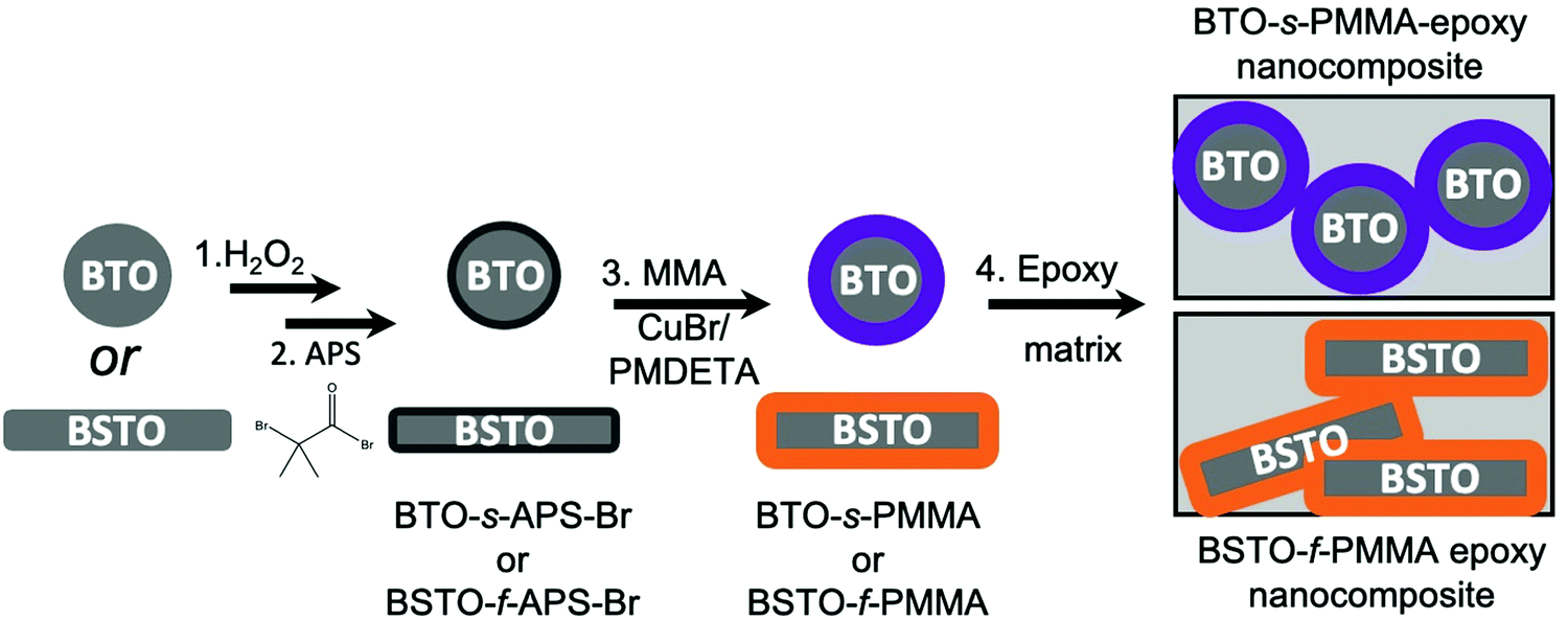 | ||
| Fig. 1 Schematic of the poly(methyl methacrylate) functionalisation strategy of BTO-s and BSTO-f to produce printable dielectric inks. | ||
To confirm successful covalent grafting of PMMA onto the nanoparticle/fibre surface and determine the thickness of the polymer layer, thermogravimetric analysis coupled to a mass spectrometer (TGA-MS), X-ray photoelectron spectroscopy (XPS), and transmission electron microscopy (TEM) were performed. A significant weight loss was observed during TGA of BTO-s-PMMA and BSTO-f-PMMA in the temperature range of 300–500 °C; the features were assigned to the pyrolysis of the organic polymer, using the mass fragments ((m/z 41 (–CH2C(CH3)–+), 59 (–COOCH3+), 69 (–CH2C(CH3)(CO)–+)) detected in both samples (Fig. 2a and d), and fall in the expected temperature range.44 The mass loss of the products (BTO-s-PMMA and BSTO-f-PMMA) compared to the as-received (BTO-s and BSTO-f) and pre-polymerisation material (BTO-s-APS-Br and BSTO-f-APS-Br) increased, corresponding to polymer grafting ratios of 13 wt% and 16 wt%, respectively (grafting ratio = weight of polymer/weight of inorganic framework).
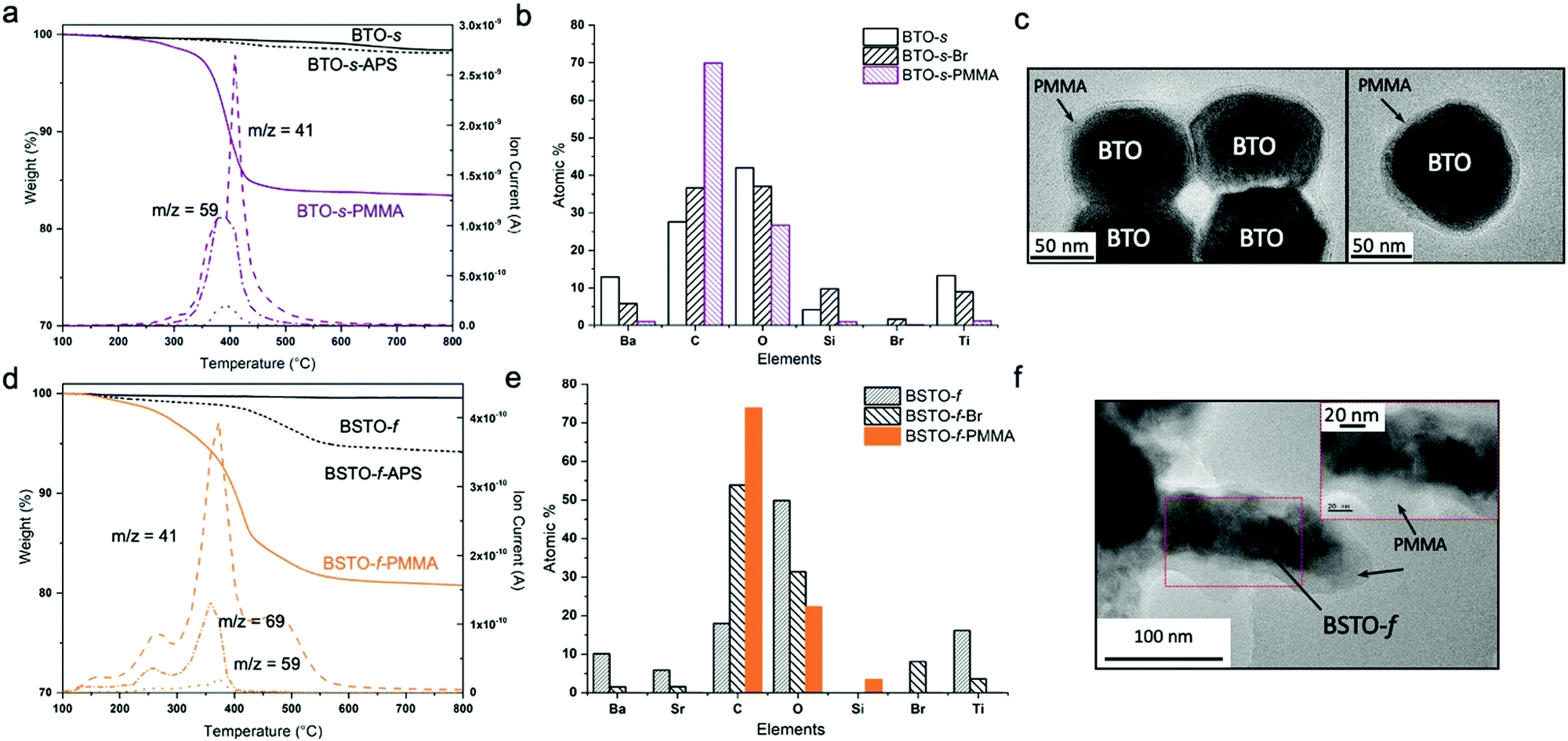 | ||
| Fig. 2 (a) TGA-MS profile of BTO-s-PMMA m/z 41 (–CH2C(CH3)–+), 59 (–COOCH3+), 69 (–CH2C(CH3)(CO)–+), (b) XPS atomic % from core level atomic spectrums of BTO-s-PMMA, (c) TEM images of the PMMA shell coating BTO-s, (d) TGA-MS profile of BSTO-f-PMMA, m/z 41 (–CH2C(CH3)–+), 59 (–COOCH3+), 69 (–CH2C(CH3)(CO)–+) (e) XPS atomic % from core level atomic spectrums of BSTO-f-PMMA and (f) TEM images of the PMMA shell coating BSTO-f. | ||
XPS data for BTO-s-PMMA and BSTO-f-PMMA also supports the successful surface particle modification at each stage of the synthesis process. There is a strong carbon signal in the raw materials (i.e. before performing any surface treatments) which can be attributed to the background support, contamination, and residual carbon from the polymer precursors used for the particle synthesis. Following initial surface treatments (–OH, –γ-APS and –Br) the atomic percentages (at%) from XPS of C, O and Br increase significantly compared to the unfunctionalised material (Fig. 2b and e). Conversely, once functionalised and coated with a surface layer of P(MMA), the at% of Ba and Ti in BTO-s and Ba, Sr and Ti in BSTO-f decreased significantly. This decrease in metal at% but increase in carbon further supports the successful polymer functionalisation, as XPS is a surface sensitive technique. In addition, the bromine signal was not detectable after the successful polymerisation of MMA by ATRP (BTO-s-PMMA and BSTO-f-PMMA; Fig. 2b and e). Finally, the polymer coating was clearly observed by TEM, which further supports the XPS results; in BTO-s-PMMA and BSTO-f-PMMA the polymer layers were approximately 9 nm and ca. 14 nm thick, respectively (Fig. 2c and f). Furthermore, the crystal structure of BSTO-f was only resolved by high resolution TEM before functionalisation and surface coating (Fig. S3a, ESI†); it was not possible to resolve the structure post-polymerisation due to the amorphous polymer coating (Fig. S3b, ESI†). FTIR was also utilised to further confirm successful grafting of PMMA onto the nanofibre surface (Fig. S4a, ESI†). Clear signals from the BSTO is detected pre- and post- PMMA functionalisation, but distinct peaks associated with PMMA are observed post-functionalisation, including a distinct band at 1150 cm−1 which can be attributed to the C–O–C stretching vibration. The sharp band at 1725 cm−1 shows the presence of the acrylate carboxyl group and the band at 1444 cm−1 can be attributed to the bending vibration of the C–H bonds of the methyl group. As the volume fraction is quite low, the FTIR signal of the polymer functionalised particles incorporated in epoxy is weak as the epoxy IR signature is strongest and masks the signal from the nanoparticles (Fig. S4b, ESI†).
Printed dielectric inks
Dispersions of functionalised BTO-s-PMMA and BSTO-f-PMMA in acetone were considerably more stable than for the raw material; after several days there was a thin sediment layer for the BSTO-f-PMMA whereas the unfunctionalised BSTO-f sedimented in a matter of hours (Fig. 3a). BTO-s-PMMA and BSTO-f-PMMA were dispersed in acetone in separate vials and incorporated into ultra low viscosity (ULV) epoxy (ca. 1 Pa s at 20 °C) at a loading volume fraction, φ = 0.05 by shear mixing. The acetone was driven off and the epoxy degassed in a vacuum oven which produced a stable ink suitable for screen printing. The functionalisation process was scaled up from ca. 2 g to 20 g so the ink could be used for printing larger area dielectrics and were stable for several months (Fig. 3b). Ink viscosities viable for screen printing are generally in the range of 0.1–10 Pa s, which given the low loading volume fraction of the nanoparticle fillers in the ULV epoxy, is in the rheological range for printing. The screen mesh and number of layers also controlled the quality of the print.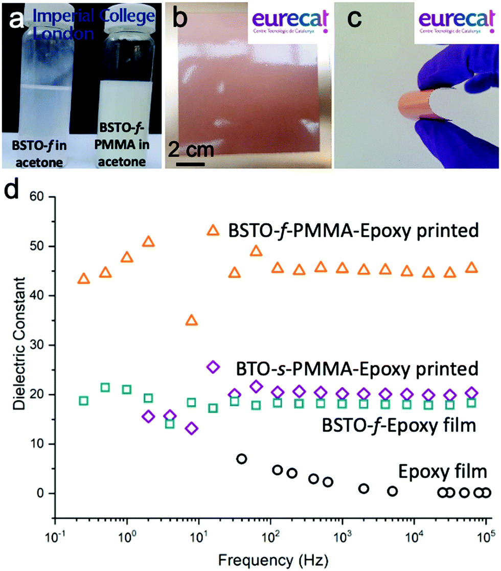 | ||
| Fig. 3 (a) Digital image of as-received BSTO-f and functionalised BSTO-f-PMMA in acetone after 48 h sedimentation, (b and c) printed dielectric films (10 × 10 cm) on flexible Cu-polyimide substrates and (d) the measured dielectric constants of printed films loading fraction, φ = 0.05. | ||
As well as utilising a low viscosity epoxy, it was also a slow cure epoxy which helped to control the printing process further, allowing for a longer working window for printing. Hardener was added to the epoxy-ceramic (BTO-s-PMMA-epoxy or BSTO-f-PMMA-epoxy) inks and printed onto Cu-polyimide films using a screen printer, optimised for mesh size and number of layers (further details below and in the experimental section). The loading of the BTO-s-PMMA and BSTO-f-PMMA in the epoxy composite dielectric films was fixed at φ = 0.05 as higher loadings resulted in increased viscosity and inks unsuitable for printing. After curing, the films were smooth, shiny and flexible and between 5–20 μm thick, with an even distribution of particles throughout the matrix (photograph in Fig. 3b and surface roughness images via AFM in Fig. S5, ESI†). It was also possible to bend and flex the dielectric films between 90–180° without cracks appearing on the surface (Fig. 3c and Fig. S5b, ESI†). Across a range of frequencies (100–105 Hz) there was a significant increase in the dielectric constant of both printed BTO-s-PMMA (ca. 21) and BSTO-f-PMMA (ca. 45) when compared to the pure epoxy film (ca. 2) (Fig. 3d). The films have a good dielectric performance, given the low content of ceramic, compared to other systems in the literature (Fig. 4); the low ceramic loading reduces cost and improves flexibility. The functionalisation with PMMA plays a significant role – more than doubling the dielectric constant of the BSTO-f-PMMA-epoxy compared to the BSTO-f-epoxy control (Fig. 3d). As expected, the increased dielectric constant was associated with a lower electrical breakdown strength (Eb). In general, there is an empirical guideline that the maximum dielectric power density (∼kEb2) does not exceed 400 MV cm−2.45 There are some remaining defects in the film surface from the printing process that can limit the breakdown strength, but the dielectric breakdown strength film tests exceed the testing range of the harvester (Table S1, ESI†), furthermore the current leakage is very low as discussed in detail below.
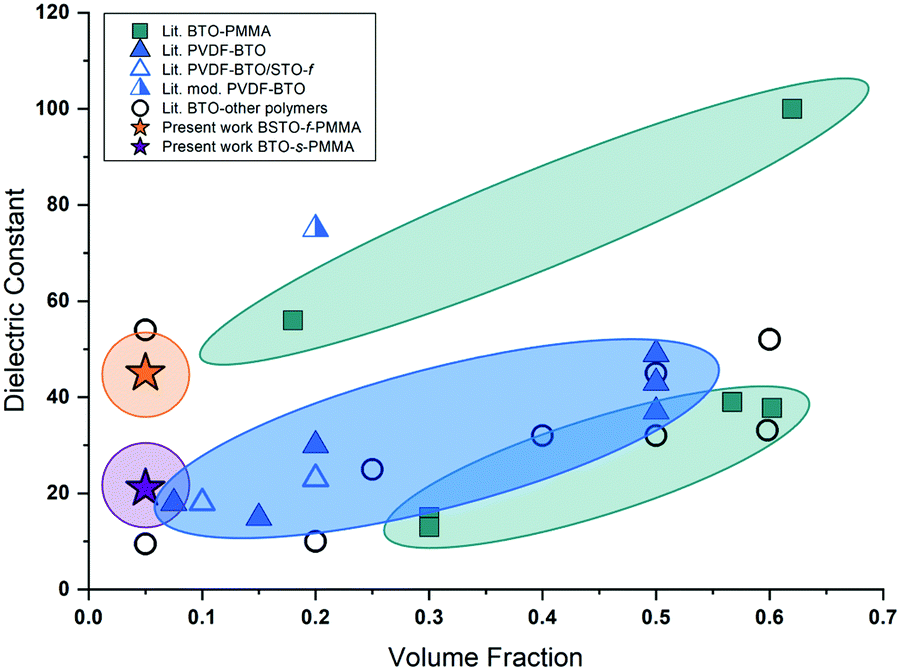 | ||
| Fig. 4 Summary of literature values of dielectric constant and volume fraction based on BTO nanocomposites. (Table S2 in ESI† contains details of the data present in the plot). | ||
Existing literature in the functionalisation of intrinsically high-k nanoparticles composites for thin film dielectric harvesters is summarised in Fig. 4 and Table S2 (ESI†), focussing on BTO and strontium titanate (STO) spherical nanoparticles. The reported dielectric constant varies widely, due to a range of contributing factors including volume fraction, degree of functionalisation of the ferroelectric ceramic particles, the type of polymer, mixing methodology, matrix type, frequency at which the dielectric properties were recorded and the composite formation process (e.g. hot press, draw-down etc.). However, a general linear trend for BTO-PVDF nanocomposites is observed for volume fractions between 0.1–0.5 with dielectric constants reported between ca. 18–42, which broadly follows the Bruggeman mixing rule46 (although it should be noted that due to variability in the way and which data is reported in literature it was not always possible to compare fairly). There appear to be two trends for PMMA functionalised BTO spherical nanoparticles. The dielectric constant of the low volume fraction BSTO-f-PMMA from this work is within the upper band of other PMMA-BTO high-k nanocomposites, suggesting an excellent microstructure.
Mechanical energy harvesting device
Following the successful printing of the dielectric nanocomposite films, the mechanical capacitive harvesting concept was investigated by combining a composite elastomer electrode and the insulating spring element,47 with the printed high-k dielectric films. In the harvester, the maximum capacitance (in the compressed state) not only depends on the thickness and permittivity of the dielectric but also on the quality of the electrode and the electrode-dielectric interface. The dielectric of the variable capacitor must not only be characterized by a high permittivity, breakdown field and low leakage currents12 but also by a high mechanical strength and wear resistance to sustain thousands to millions of pressure cycles.The influence of the dielectric printing parameters and elastomer electrode behaviour were tested first. Stencil printed 1 × 1 cm2 large 120–200 μm thick layers of the commercial conducting elastomer ELASTOSIL® LR 3162 were fabricated as elastomer contacts. A maximum applied pressure of 40 N cm−2 was selected to represent the approximate range accessible with a thumb press or heel strike. Using the conductive elastomer electrode rather than a directly deposited metal (Ag) contact produced a slightly lower capacitance (reduced by 18–21%); however, the values are very encouraging given the particulate filler in the elastomer (Fig. 5a). The use of a higher mesh count (110T is the mesh count per centimetre) during the dielectric screen printing resulted in thinner dielectric layers and therefore higher capacitance (Fig. 5b). In all cases, the use of BSTO-f-PMMA resulted in higher capacitance compared to BTO-s-PMMA (Fig. 5c). Using a double layer print, only marginally increased the dielectric thickness from 10–12 μm to 13–15 μm, but increased the capacitance, presumably by creating a more uniform film (Fig. 5c). The observed capacitance scaled nearly linearly with the applied mechanical pressure from 5 N cm−2 up to 30 N cm−2 (Fig. 5d).
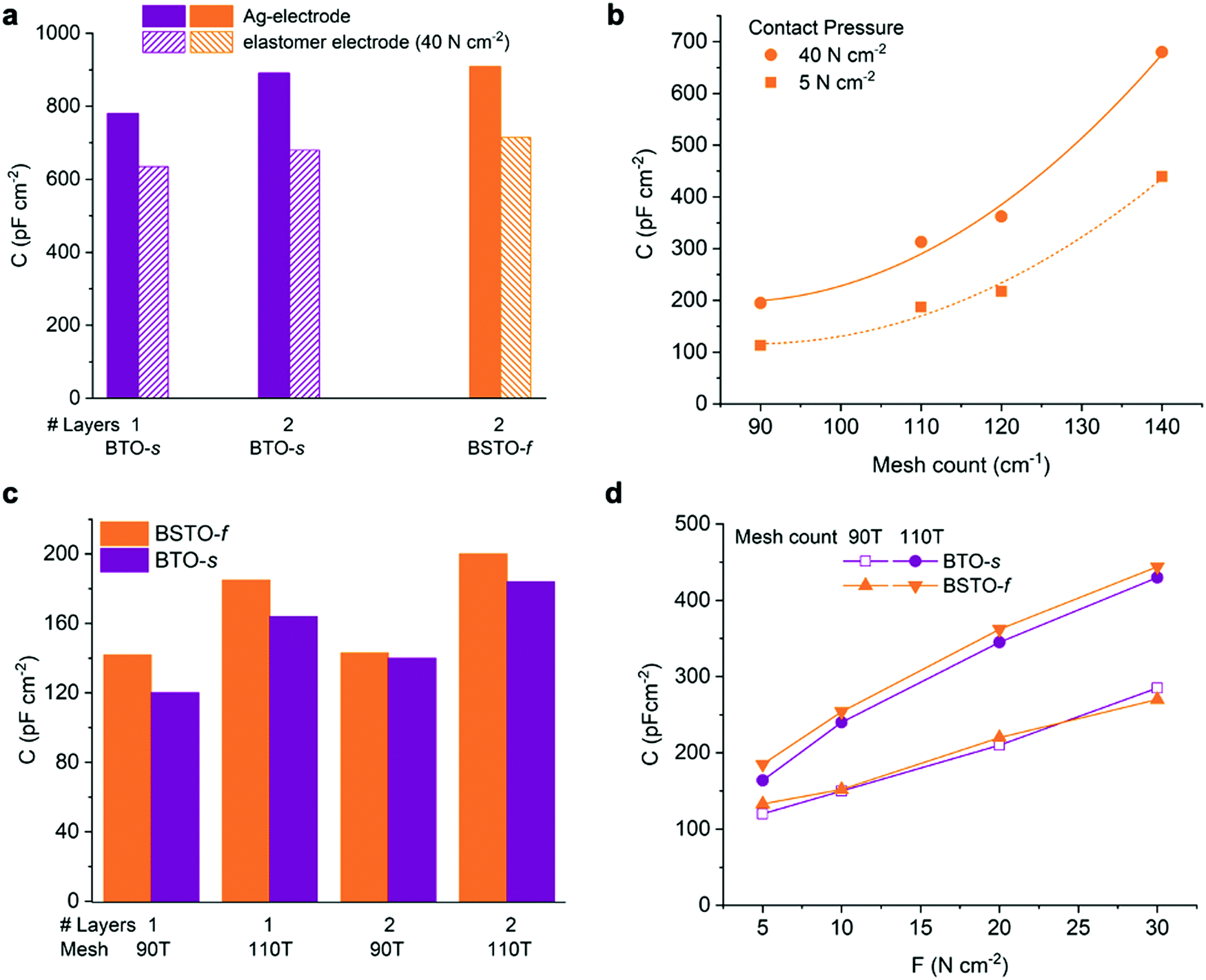 | ||
| Fig. 5 (a) A real capacity (at 1 kHz) as function of the top electrode (deposited Ag versus elastomer at 40 N cm−2) layers indicare the number of printed layers, (b) as function of screen print mesh count for the dielectric print, (c) as function of material, layer number and mesh count at 5 N cm−2 contact pressure, (d) as function of contact pressure. | ||
The final harvester design is shown in Fig. 6. An elastic silicone spring element was printed inside the conductive elastomer electrode area to promote rapid detachment between electrode and dielectric after pressure release.47 Electrodes and dielectric patches of 1 cm2 were printed on flexible substrate strips that were folded in a stack of three parallel connected capacitors (Fig. 6b and Fig. S5b, c, ESI†). All devices were encapsulated in a polymer pouch to avoid contamination of the interface (Fig. 6c, d and Fig. S5d, ESI†). A maximum capacity of ca. 1.5 nF was achieved at a pressure of 50 N with the three-capacitor stack device.
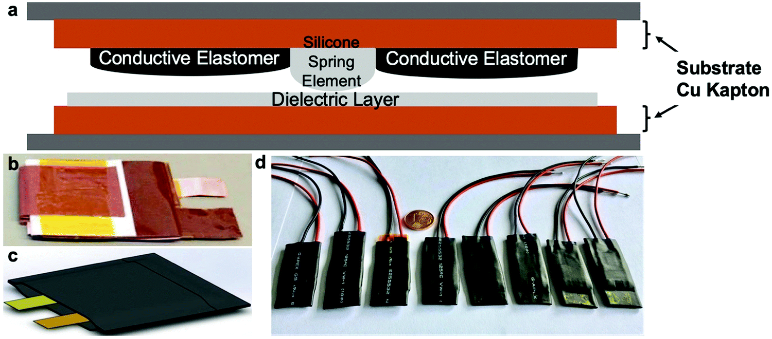 | ||
| Fig. 6 Energy harvesting demonstrator, (a) cross section, (b) capacitor stacking by folding of dielectric and electrode foils; the active area is 1 cm2 for each layer in the stack, (c and d) encapsulated devices. | ||
A large number of devices were fabricated with material variations to study the long-term cycling behaviour. The diode circuit (Fig. 7c) was used to study the energy harvesting behaviour. Electricity is generated by simply lifting the voltage of the charges from V1 to a higher voltage V2
| Q = V1·Cvar–max | (1) |
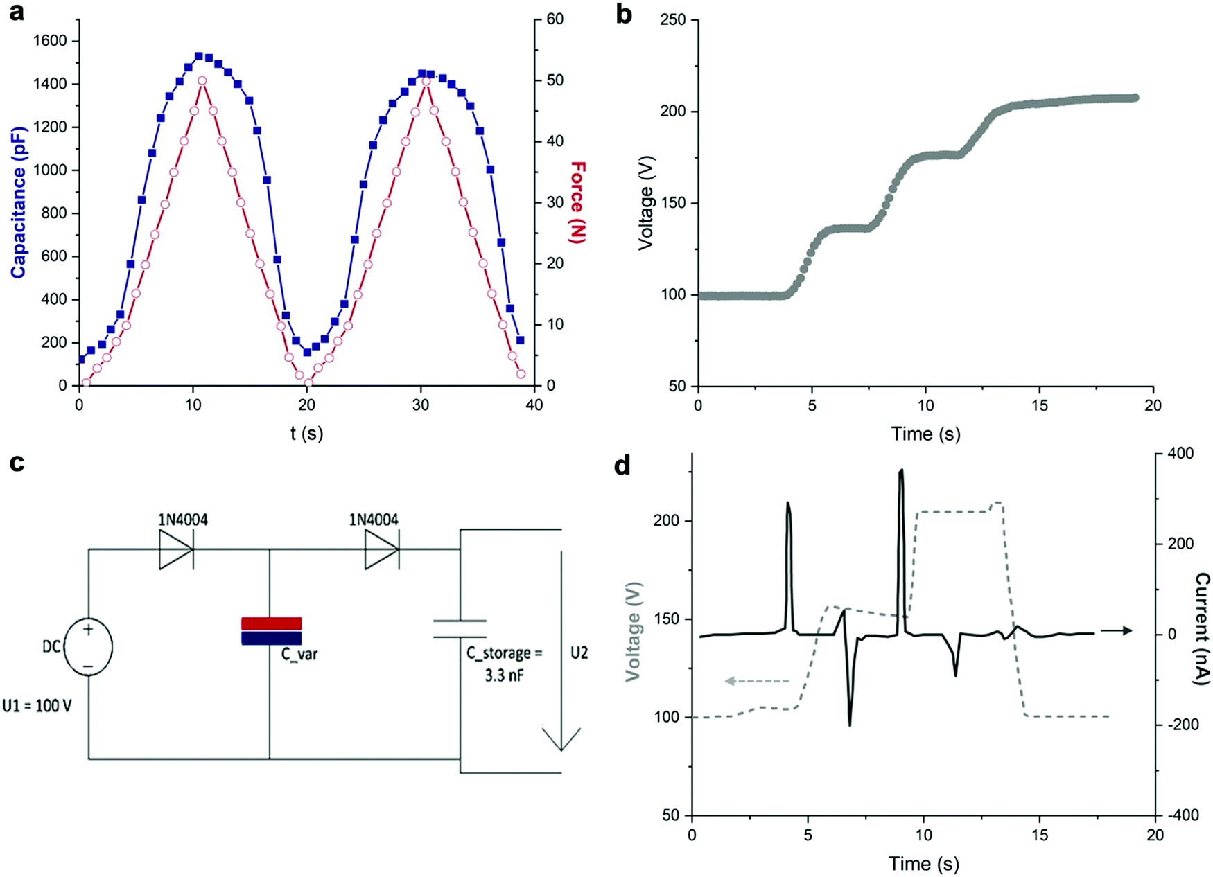 | ||
| Fig. 7 (a) Characteristic of a three-layer capacitor stack according to Fig. 6d, (b) output voltage of the harvester device with the parameters: Clow = 180 pF, Chigh = 1550 pF, Ileakage = 15 nA, (c) harvester test circuit, (d) output voltage and current through the variable capacitor for a single layer with Cmax = 508 pF. Data reanalysed from.48 | ||
A significant improvement in the performance of the harvester in terms of durability and cyclability was achieved with the polymer functionalised nanocomposite dielectric materials. The capacitance in the loaded state (Table 1) is similar (ca. 1.4 nF) in all cases of dielectric but the leakage current was considerably reduced using the PMMA-functionalised dielectric particles. The leakage current was lower for freshly prepared devices after cycling; several samples of unfunctionalised dielectrics showed a dramatically increased leakage current by a factor of 100–1000 after cycling, due to mechanical failures associated with particle agglomerates in the films, which the PMMA functionalisation reduces.
| Sample | C (0N) (nF) | C (40N) (nF) | I leak (0N) (nA) | I leak (20N) (nA) | I leak (20N) (nA) > 1000 cycles |
|---|---|---|---|---|---|
| a See ref. 12 for further details, B2 = batch 2 (2 layers, 110T mesh), 1L = 1 printed layer (110T Mesh), 2L = 2 printed layers (110T mesh), Ileak = leakage current. | |||||
| Non-functionalised dielectrica | |||||
| STO-B2 | 0.059 | 1.4 | 2 | 3–7 | 20–30 |
| STO-B2 | 0.057 | 1.5 | <1 | 10–20 | 3400 |
| STO-B2 | 0.057 | 1.4 | 6 | 10–20 | 1000 |
| Functionalised dielectric films | |||||
| BTO-s 1L | 0.043 | 1.0 | 1.7 | 1–7 | 20–30 |
| BTO-s 2L | 0.046 | 1.4 | 1.0 | 3–7 | 5–10 |
| BSTO-f 2L | 0.061 | 1.5 | < 1 | 3–5 | 8–15 |
The power of the harvester depends on the maximum accessible frequency. With the current elastomer electrode and integrated spring elements a working frequency of 0.5 Hz was achieved. The energy of one harvesting cycle with the diode circuit is;
| E = Cmax·V12 | (2) |
| 0.5 Hz | V 1 = 10 V | V 1 = 100 V |
|---|---|---|
| P | 75 nW | 7.5 μW |
| Power density | 1.6 μW cm−3 | 160 μW cm−3 |
Conclusions
Printable epoxy-based nanocomposite inks were prepared by using core–shell structured BSTO-f-PMMA and BTO-s-PMMA nanoparticles as fillers. After characterisation, the successful covalent functionalisation of PMMA with BTO and BSTO resulted in stable nanoparticle dispersions and increased compatibility with epoxy. The nanocomposites exhibit significantly enhanced dielectric constants and low leakage current when compared to the epoxy film alone. In addition, when compared to BTO-s-PMMA-epoxy films, the BSTO-f-PMMA films exhibited a higher dielectric constant. The printed dielectric films were configured into a mechanical energy harvesting device containing flexible conducting elastomers separated by insulating spring elements to maximise capacitance variance as a function of applied pressure. The printed functionalised dielectric films showed high mechanical cycling stability and low leakage current, much improved over the state-of-the-art materials. The harvester performed well over 1000 converting cycles, consistently producing a power density of 160 μW cm−3 at a frequency of 0.5 Hz. Such devices can be reliably used as energy harvesters that convert mechanical into electrical energy and this work has demonstrated that they can be utilised in wearable electronic applications in the future.Experimental
Materials
BaTiO3 nanoparticles were purchased from Sigma-Aldrich UK and Ba(0.6)Sr(0.4)TiO3 nanofibres were supplied by Pardam, Czech Republic. Hydrogen peroxide (H2O2), methyl methacrylate (MMA), copper(I) bromide (CuBr), acetone, toluene, methylene chloride (CH2Cl2), N,N-dimethyl formamide (DMF), 2-bromo-2-methylpropionyl bromide, N,N,N′,N′′,N′′-pentamethyldiethylenetriamine (PMDETA), γ-amino-propyl triethoxysilane (γ-APS) were purchased from Sigma-Aldrich UK. Methyl methacrylate was previously purified by passing the monomer through an alumina column to remove stabilizers and then degassed via a freeze–pump–thaw method and dried over 3 Å sieves (20 vol%) and kept under nitrogen. Prime™ 20ULV epoxy was purchased from Gurit with a slow (ULV) hardener. Holey carbon films on 300 mesh copper grids used for TEM experiments were purchased from Elektron Technology UK Ltd. Aluminium oxide 90 active neutral was provided by Merck UK. All gases supplied by BOC, UK.Preparation of brominated BTO-s and BSTO-f
In a typical experiment, following previous literature procedures for the PMMA functionalisation of nanomaterials,25,43 the nanoparticles surface was first hydrolysed: 10 g of either BTO-s or BSTO-f and 70 ml aqueous solution of H2O2 (30 wt%) were combined in a round-bottomed flask. The materials were sonicated for 30 minutes to suspend the nanoparticles and then refluxed at 105 °C for 4 h. The nanoparticles were recovered by centrifugation at 10![[thin space (1/6-em)]](https://www.rsc.org/images/entities/char_2009.gif) 000g for 10 minutes and washed three times with deionized water. The particles were then dried under vacuum at 80 °C for 10 h. 5 g of the hydroxylated nanoparticles or fibres were suspended in 50 ml of anhydrous toluene and sonicated for 15 minutes; 2.5 g of γ-APS was added and the mixture heated to 80 for 24 h under a N2 atmosphere. The nanoparticles were recovered by centrifugation at 10000g and washed twice with toluene (resulting in BTO-s-APS and BSTO-f-APS). After drying, the obtained particles (2 g) or fibres were combined trimethylamine, the CH2Cl2 which contained 0.28 g of 2-bromo-2-methylpropionyl bromide was then added dropwise at 0 °C over 1 h and stirred at maintained temperature for 2 h and then left overnight. The nano-particles or -fibres (BTO-s-Br and BSTO-f-Br respectively) were then recovered by centrifugation at 10000g for 10 minutes and washed three times with CH2Cl2. After drying, the brominated particles were yellowed in colour (compared to the original white powder) and stored under N2.
000g for 10 minutes and washed three times with deionized water. The particles were then dried under vacuum at 80 °C for 10 h. 5 g of the hydroxylated nanoparticles or fibres were suspended in 50 ml of anhydrous toluene and sonicated for 15 minutes; 2.5 g of γ-APS was added and the mixture heated to 80 for 24 h under a N2 atmosphere. The nanoparticles were recovered by centrifugation at 10000g and washed twice with toluene (resulting in BTO-s-APS and BSTO-f-APS). After drying, the obtained particles (2 g) or fibres were combined trimethylamine, the CH2Cl2 which contained 0.28 g of 2-bromo-2-methylpropionyl bromide was then added dropwise at 0 °C over 1 h and stirred at maintained temperature for 2 h and then left overnight. The nano-particles or -fibres (BTO-s-Br and BSTO-f-Br respectively) were then recovered by centrifugation at 10000g for 10 minutes and washed three times with CH2Cl2. After drying, the brominated particles were yellowed in colour (compared to the original white powder) and stored under N2.
ATRP of MMA with brominated BTO-s and BSTO-f
1.8 g of BTO-s-Br or BSTO-f-Br was suspended in 50 ml of DMF in a round-bottomed flask and sonicated for 15 minutes. 0.22 g of CuBr was added and seal. Oxygen in the flask was removed by evacuating and back-filling with N2 at least 3 times. Degassed MMA (in excess) and 0.28 g of PMDETA were added by syringe through a suba-seal. The mixture was stirred at 60 °C overnight. The polymer functionalised BTO-s or BSTO-f (namely BTO-s-PMMA and BSTO-f-PMMA) were recovered by centrifugation at 10000g for 10 minutes and washed with clean acetone 3 times to remove any unreacted monomer and adsorbed polymer and then stored in acetone. PMMA functionalised nano-particles and – fibres were loaded into epoxy by shear mixing at various loadings, the acetone was driven off and the epoxy degassed in a vacuum oven, before adding hardener at a ratio of 1:0.23 resin:hardener. After curing, dielectric inks where then ready for printing and/or casting onto Cu/polyimide flexible foils. The inks were printed using an ATMA flat screen printer (AT-80P/B) and 110T (mesh count per cm) polyester screen mesh with a distance of 3 mm between the screen and substrate (Cu/polyimide foil). The film thicknesses were determined using a VEECO profilometer and (after printing two consecutive layers) the thicknesses were between 5–10 μm. FTIR of polymer functionalised particles and printed films were measured with a PerkinElmer Frontier instrument.
Dielectric film characterisation
TGA was performed using a Mettler Toledo TGA-DSC 1 integrated with a Hiden HPR-20 QIC EGA mass spectrometer under a N2 atmosphere. Samples were held at 100 °C for 30 min under N2 flow of 60 ml min−1 and then ramped at 10 °C min−1 to 800 °C. XRD measurements were carried out using dried powder samples. Data were processed using Polymer Laboratories Cirrus software. These samples were loaded onto zero-background silicon XRD sample holders. The measurement was recorded at a scan rate of 0.108°/s with the Cu Kα (1.542 Å) line using a PANalytical X’Pert PRO diffractometer. All XPS spectra were recorded using a K-alpha+ XPS spectrometer equipped with a MXR3 Al Kα monochromated X-ray source (hν = 1486.6 eV). X-Ray gun power was set to 72 W (6 mA and 12 kV). Argon etching of the samples was done using the standard EX06 argon ion source using 500 V accelerating voltage and 1 μA ion gun current. Survey scans were acquired using 200 eV pass energy, 1 eV step size, and 100 ms (50 ms × 2 scans) dwell times. All high-resolution spectra were acquired using 20 eV pass energy, 0.1 eV step size, and 1 s (50 ms × 20 scans = 1000 ms) dwell times. Samples were prepared by pressing the sample onto double-side sticky carbon-based tape. Pressure during the measurement of XPS spectra was ≤1 × 10⁻⁸ mbar. Casa XPS software (version 2.3.16) was used to process the data. Scanning electron microscopy (SEM) micrographs were taken with a LEO Gemini 1525 FEGSEM (Zeiss, Germany) controlled by SmartSEM software, with a working distance of ca. 7 mm, accelerating voltage of 10 keV, and a 30 μm aperture using an InLens detector. Tapping-mode Veeco Multimode VIII AFM with Nanoscope IV Digital Instruments AFM controller (Bruker, USA) using Nanosensor tapping mode probes (Windsor Scientific Ltd, UK) was used to characterise deposited films. AFM micrographs were processed in NanoScope Analysis (v1.40, Bruker), using 3rd order flattening (5% z-threshold) followed by spike removal (value 3.00). Transmission Electron Microscopy (TEM) was carried out using a JEOL2100Plus TEM at 200 kV operating voltage. Typically, dielectric films were coated with Au of 1 cm × 1 cm area (by sputtering) and capacitance and dielectric constants were recorded using a DS6000 Dielectric Thermal Analyser (Lacerta Technologies) and Reference 600 Potentiostat, Gamry Instruments. Electrical breakdown strength was measured using a Spellman SL600 high voltage power supply on Au coated dielectric films.Energy harvester measurements
The harvesters were made following the steps of.48 The elastomer-electrode was prepared with help of an electrically conductive silicone rubber “ELASTOSIL® LR 3162 A/B” (Wacker Chemie AG), a two-component compound with short curing time. The electrical conductivity is 11 Ω cm−1 and the viscosity is 6600 Pas according to the data sheet. Doctor blade as well as screen printing was used to deposit the material on copper foil or flexible printed circuit board material. A 3 h curing process was completed at 70 °C. Dielectric and elastomer electrode foils (process shown in (Fig. S5, ESI†) were mounted in a mechanical cycling station that allowed to adjust the maximum force and cycle frequency. All measured samples had a size of 10 × 10 mm2. The capacity as function of the applied force was measured with help of Agilent 4284A RLC meter. The leakage current was measured at 100 V with Keithley 2450 source meter. A steady state value was achieved after ca. 3 min. For current/charge measurements according,48,52 the source meter was used as input voltage source (Vin = 100 V) and for measurement of the input current. The output current was measured over RL with help of the oscilloscope 3012(B). In a second configuration the Zener diode D2 was replaced with a diode identical to D1 and RL was replaced by a 3.3 nF capacitor. The transferred charges were calculated based on the increase of the voltage at the output capacitor.Author contributions
Conceptualisation: H. S. L, R. H., L.G., M. S. P. S., Q. J., A. B.; writing – original draft H. S. L., R. H., M. S. P. S., data curation: H. S. L, M. T., L. V., L. G., N. R., Q. J., E. R., H. C. Y.; formal analysis: H. S. L., L. G., R. H.; funding acquisition: M. S. P. S., R. H., A. B., J. B.; methodology: H. S. L., R. H.; writing – review & editing, all authors.Conflicts of interest
There are no conflicts to declare.Acknowledgements
We would like to thank the EU FP7 project (#604093) MatFlexEnd for the funding. H. S. L. would like to thank Dr Mohammad Reza Bahmanyar at ICL for discussions and support on electrical breakdown measurements. The authors thank the editors and reviewers for their constructive insightful comments which improved the manuscript. The authors thank the editor and reviewers for their constructive comments which improved the manuscript.References
- L. Atzori, A. Iera and G. Morabito, The Internet of Things: A survey, Comp. Networks, 2010, 54, 2787–2805, DOI:10.1016/j.comnet.2010.05.010.
- J. A. Rogers, T. Someya and Y. Huang, Materials and Mechanics for Stretchable Electronics, Science, 2010, 327, 1603–1607, DOI:10.1126/science.1182383.
- Z. L. Wang and W. Wu, Nanotechnology-Enabled Energy Harvesting for Self-Powered Micro-/Nanosystems, Angew. Chem., Int. Ed., 2012, 51, 11700–11721, DOI:10.1002/anie.201201656.
- B. Wang, et al., High-k Gate Dielectrics for Emerging Flexible and Stretchable Electronics, Chem. Rev., 2018, 118, 5690–5754, DOI:10.1021/acs.chemrev.8b00045.
- G. Moretti, S. Rosset, R. Vertechy, I. Anderson and M. Fontana, A Review of Dielectric Elastomer Generator Systems, Adv. Intell. Syst., 2020, 2, 2000125, DOI:10.1002/aisy.202000125.
- T. Krupenkin and J. A. Taylor, Reverse electrowetting as a new approach to high-power energy harvesting, Nat. Commun., 2011, 2, 448, DOI:10.1038/ncomms1454.
- K. Panchadar, D. West, J. A. Taylor and T. Krupenkin, Mechanical energy harvesting using a liquid metal vortex magnetohydrodynamic generator, Appl. Phys. Lett., 2019, 114, 093901, DOI:10.1063/1.5078384.
- Y.-Z. Zhang, et al., Printed supercapacitors: materials, printing and applications, Chem. Soc. Rev., 2019, 48, 3229–3264, 10.1039/C7CS00819H.
- D. Li, W.-Y. Lai, Y.-Z. Zhang and W. Huang, Printable Transparent Conductive Films for Flexible Electronics, Adv. Mater., 2018, 30, 1704738, DOI:10.1002/adma.201704738.
- D. Li, W.-Y. Lai, F. Feng and W. Huang, Post-Treatment of Screen-Printed Silver Nanowire Networks for Highly Conductive Flexible Transparent Films, Adv. Mater. Interfaces, 2021, 8, 2100548, DOI:10.1002/admi.202100548.
- T. Cheng, et al., Inkjet-Printed High-Performance Flexible Micro-Supercapacitors with Porous Nanofiber-Like Electrode Structures, Small, 2019, 15, 1901830, DOI:10.1002/smll.201901830.
- R. Hahn, et al. , Energy Harvest. Syst., 2016, 3, 277–285 CrossRef.
- S. Gao, et al., Wearable high-dielectric-constant polymers with core–shell liquid metal inclusions for biomechanical energy harvesting and a self-powered user interface, J. Mater. Chem. A, 2019, 7, 7109–7117, 10.1039/C9TA01249D.
- A. Kumar, R. Kiran, V. S. Chauhan, R. Kumar and R. Vaish, Piezoelectric energy harvester for pacemaker application: a comparative study, Mater. Res. Express, 2018, 5, 075701, DOI:10.1088/2053-1591/aab456.
- L. Dong, et al., Flexible Porous Piezoelectric Cantilever on a Pacemaker Lead for Compact Energy Harvesting, Adv. Mater. Technol., 2019, 4, 1800148, DOI:10.1002/admt.201800148.
- J. Wang, et al., Sustainably powering wearable electronics solely by biomechanical energy, Nat. Commun., 2016, 7, 12744, DOI:10.1038/ncomms12744.
- J.-H. Bahk, H. Fang, K. Yazawa and A. Shakouri, Flexible thermoelectric materials and device optimization for wearable energy harvesting, J. Mater. Chem. C, 2015, 3, 10362–10374, 10.1039/C5TC01644D.
- W. Wu, et al., Lead Zirconate Titanate Nanowire Textile Nanogenerator for Wearable Energy-Harvesting and Self-Powered Devices, ACS Nano, 2012, 6, 6231–6235, DOI:10.1021/nn3016585.
- J. Zhao and Z. You, A Shoe-Embedded Piezoelectric Energy Harvester for Wearable Sensors, Sensors, 2014, 14, 12497–12510 CrossRef CAS PubMed.
- D. Sitko, et al., Dielectric properties of BaTiO 3 based materials with addition of transition metal ions with variable valence, IOP Conf. Ser.: Mater. Sci. Eng., 2013, 49, 012050 CrossRef CAS.
- T. Remmel, R. Gregory and B. Baumert, Characterization of Barium Strontium Titanate Films Using XRD, JCPDS Int. Centre Diffrat. Data, 1999, 38–45 CAS.
- V. S. Puli, et al., Core-shell like structured barium zirconium titanate-barium calcium titanate–poly(methyl methacrylate) nanocomposites for dielectric energy storage capacitors, Polymer, 2016, 105, 35–42, DOI:10.1016/j.polymer.2016.10.020.
- T. Wang, et al., Preparation of a hybrid core–shell structured BaTiO3@PEDOT nanocomposite and its applications in dielectric and electrode materials, Appl. Surf. Sci., 2015, 356, 232–239, DOI:10.1016/j.apsusc.2015.08.077.
- K. Yang, et al., Combining RAFT Polymerization and Thiol–Ene Click Reaction for Core–Shell Structured Polymer@BaTiO3 Nanodielectrics with High Dielectric Constant, Low Dielectric Loss, and High Energy Storage Capability, ACS Appl. Mater. Interfaces, 2014, 6, 1812–1822, DOI:10.1021/am4048267.
- L. Xie, X. Huang, C. Wu and P. Jiang, Core-shell structured poly(methyl methacrylate)/BaTiO3 nanocomposites prepared by in situ atom transfer radical polymerization: a route to high dielectric constant materials with the inherent low loss of the base polymer, J. Mater. Chem., 2011, 21, 5897–5906, 10.1039/C0JM04574H.
- L. Xie, X. Huang, K. Yang, S. Li and P. Jiang, “Grafting to” route to PVDF-HFP-GMA/BaTiO3 nanocomposites with high dielectric constant and high thermal conductivity for energy storage and thermal management applications, J. Mater. Chem. A, 2014, 2, 5244–5251, 10.1039/c3ta15156e.
- K. Brandt, C. Neusel, S. Behr and G. A. Schneider, Dielectric behaviour and conductivity of high-filled BaTiO3–PMMA composites and the facile route of emulsion polymerization in synthesizing the same, J. Mater. Chem. C, 2013, 1, 3129–3137, 10.1039/C3TC30204K.
- K. Hayashida, Y. Matsuoka and Y. Takatani, An ideal nanostructure of polymer/BaTiO3 dielectric materials with high reliability for breakdown strength: isolated and uniformly dispersed BaTiO3 nanoparticles by thick polymer shells, RSC Adv., 2014, 4, 33530–33536, 10.1039/C4RA06801G.
- L. Xie, X. Huang, Y. Huang, K. Yang and P. Jiang, Core@Double-Shell Structured BaTiO3–Polymer Nanocomposites with High Dielectric Constant and Low Dielectric Loss for Energy Storage Application, J. Phys. Chem. C., 2013, 117, 22525–22537, DOI:10.1021/jp407340n.
- M. Ejaz, et al., Core-shell structured poly(glycidyl methacrylate)/BaTiO3 nanocomposites prepared by surface-initiated atom transfer radical polymerization: A novel material for high energy density dielectric storage, J. Polym. Sci., Part A: Polym. Chem., 2015, 53, 719–728, DOI:10.1002/pola.27485.
- D. Wang, et al., Dielectric properties of polystyrene based composites filled with core-shell BaTiO/polystyrene hybrid nanoparticles, IEEE Trans. Dielectr. Electr. Insul., 2014, 21, 1438–1445, DOI:10.1109/TDEI.2013.004329.
- X. Zhang, Y. Ma, C. Zhao and W. Yang, High Dielectric Performance Composites with a Hybrid BaTiO3/Graphene as Filler and Poly(vinylidene fluoride) as Matrix, ECS J. Solid State Sci. Technol., 2015, 4, N47–N54, DOI:10.1149/2.0291505jss.
- D. Yu, N.-x. Xu, L. Hu, Q.-l. Zhang and H. Yang, Nanocomposites with BaTiO3–SrTiO3 hybrid fillers exhibiting enhanced dielectric behaviours and energy-storage densities, J. Mater. Chem. C, 2015, 3, 4016–4022, 10.1039/C4TC02972K.
- P. Kim, et al., Phosphonic Acid-Modified Barium Titanate Polymer Nanocomposites with High Permittivity and Dielectric Strength, Adv. Mater., 2007, 19, 1001–1005, DOI:10.1002/adma.200602422.
- S. Liu, S. Xue, S. Xiu, B. Shen and J. Zhai, Surface-modified Ba(Zr0.3Ti0.7)O3 nanofibers by polyvinylpyrrolidone filler for poly(vinylidene fluoride) composites with enhanced dielectric constant and energy storage density, Sci. Rep., 2016, 6, 26198, DOI:10.1038/srep26198.
- N. Xu, Q. Zhang, H. Yang, Y. Xia and Y. Jiang, In-situ preparation of hierarchical flower-like TiO2/carbon nanostructures as fillers for polymer composites with enhanced dielectric properties, Sci. Rep., 2017, 7, 43970, DOI:10.1038/srep43970.
- L. Shaohui, Z. Jiwei, W. Jinwen, X. Shuangxi and Z. Wenqin, Enhanced Energy Storage Density in Poly(Vinylidene Fluoride) Nanocomposites by a Small Loading of Suface-Hydroxylated Ba0.6Sr0.4TiO3 Nanofibers, ACS Appl. Mater. Interfaces, 2014, 6, 1533–1540, DOI:10.1021/am4042096.
- X. Huang, B. Sun, Y. Zhu, S. Li and P. Jiang, High-k polymer nanocomposites with 1D filler for dielectric and energy storage applications, Prog. Mater. Sci., 2019, 100, 187–225, DOI:10.1016/j.pmatsci.2018.10.003.
- L. Zhang, J. Zhai and X. Yao, Dielectric properties of barium strontium titanate thick films prepared by electrophoretic deposition, Mater. Res. Bull., 2009, 44, 1058–1061, DOI:10.1016/j.materresbull.2008.10.014.
- Y. Lin, Z. Zhou and H. A. Sodano, Barium titanate and barium strontium titanate coated carbon fibers for multifunctional structural capacitors, J. Compos. Mater., 2013, 47, 1527–1533, DOI:10.1177/0021998312449029.
- B. Su and T. W. Button, Microstructure and dielectric properties of Mg-doped barium strontium titanate ceramics, J. Appl. Phys., 2004, 95, 1382–1385, DOI:10.1063/1.1636263.
- L. Xie, X. Huang, K. Yang, S. Li and P. Jiang, “Grafting to” route to PVDF-HFP-GMA/BaTiO3 nanocomposites with high dielectric constant and high thermal conductivity for energy storage and thermal management applications, J. Mater. Chem. A, 2014, 2, 5244–5251, 10.1039/C3TA15156E.
- N. Rubio, et al., Grafting from versus Grafting to Approaches for the Functionalization of Graphene Nanoplatelets with Poly(methyl methacrylate), Macromolecules, 2017, 50, 7070–7079, DOI:10.1021/acs.macromol.7b01047.
- G. Gonçalves, et al., Graphene oxide modified with PMMA via ATRP as a reinforcement filler, J. Mater. Chem., 2010, 20, 9927–9934, 10.1039/C0JM01674H.
- P. Jain and E. J. Rymaszewski, Embedded thin film capacitors-theoretical limits, IEEE Trans. Adv. Packag., 2002, 25, 454–458, DOI:10.1109/TADVP.2002.806800.
- T. Gric and O. Hess, in Phenomena of Optical Metamaterials, ed. T. Gric and O. Hess, Elsevier, 2019, pp. 41–73 Search PubMed.
- Q. Jiang, H. Barkan, A. Menner and A. Bismarck, Micropatterned, macroporous polymer springs for capacitive energy harvesters, Polymer, 2017, 126, 419–424, DOI:10.1016/j.polymer.2017.04.018.
- R. Hahn, et al., Variable Capacitor Energy Harvesting Based on Polymer Dielectric and Composite Electrode, Energy Harvest. Syst., 2016, 3, 277–285, DOI:10.1515/ehs-2016-0008.
- U. Erturun, A. A. Eisape, S. H. Kang and J. E. West, Energy harvester using piezoelectric nanogenerator and electrostatic generator, Appl. Phys. Lett., 2021, 118, 063902, DOI:10.1063/5.0030302.
- M. Zhou, M. S. H. Al-Furjan, J. Zou and W. Liu, A review on heat and mechanical energy harvesting from human – Principles, prototypes and perspectives, Renewable Sustainable Energy Rev., 2018, 82, 3582–3609, DOI:10.1016/j.rser.2017.10.102.
- N. Sezer and M. Koç, A comprehensive review on the state-of-the-art of piezoelectric energy harvesting, Nano Energy, 2021, 80, 105567, DOI:10.1016/j.nanoen.2020.105567.
- V. Dorzhiev, et al., Electret-Free Micromachined Silicon Electrostatic Vibration Energy Harvester With the Bennet's Doubler as Conditioning Circuit, IEEE Electron Device Lett., 2015, 36, 183–185, DOI:10.1109/LED.2014.2387213.
Footnote |
| † Electronic supplementary information (ESI) available. See DOI: 10.1039/d1ma00661d |
| This journal is © The Royal Society of Chemistry 2022 |