
 Open Access Article
 This Open Access Article is licensed under a
 Creative Commons Attribution 3.0 Unported Licence
Live single cell imaging assays in glass microwells produced by laser-induced deep etching†
Niklas
Sandström
 *a,
Ludwig
Brandt
a,
Patrick A.
Sandoz
a,
Chiara
Zambarda
a,
Karolin
Guldevall
a,
Malte
Schulz-Ruhtenberg
b,
Bernd
Rösener
b,
Robin A.
Krüger
b and
Björn
Önfelt
*ac
*a,
Ludwig
Brandt
a,
Patrick A.
Sandoz
a,
Chiara
Zambarda
a,
Karolin
Guldevall
a,
Malte
Schulz-Ruhtenberg
b,
Bernd
Rösener
b,
Robin A.
Krüger
b and
Björn
Önfelt
*ac
aDepartment of Applied Physics, Science for Life Laboratory, KTH Royal Institute of Technology, Stockholm, Sweden. E-mail: sniklas@kth.se; onfelt@kth.se
bLPKF Laser & Electronics AG, Germany
cDepartment of Microbiology, Tumour and Cell Biology, Karolinska Institutet, Stockholm, Sweden
First published on 7th April 2022
Abstract
Miniaturization of cell culture substrates enables controlled analysis of living cells in confined micro-scale environments. This is particularly suitable for imaging individual cells over time, as they can be monitored without escaping the imaging field-of-view (FoV). Glass materials are ideal for most microscopy applications. However, with current methods used in life sciences, glass microfabrication is limited in terms of either freedom of design, quality, or throughput. In this work, we introduce laser-induced deep etching (LIDE) as a method for producing glass microwell arrays for live single cell imaging assays. We demonstrate novel microwell arrays with deep, high-aspect ratio wells that have rounded, dimpled or flat bottom profiles in either single-layer or double-layer glass chips. The microwells are evaluated for microscopy-based analysis of long-term cell culture, clonal expansion, laterally organized cell seeding, subcellular mechanics during migration and immune cell cytotoxicity assays of both adherent and suspension cells. It is shown that all types of microwells can support viable cell cultures and imaging with single cell resolution, and we highlight specific benefits of each microwell design for different applications. We believe that high-quality glass microwell arrays enabled by LIDE provide a great option for high-content and high-resolution imaging-based live cell assays with a broad range of potential applications within life sciences.
1. Introduction
Single cell biology has gained enormous interest and traction in the last decade, enabled by strong developments in different disciplines of engineering, biotechnology, and bioinformatics. Assays for single cells allow a differentiated insight into cell populations compared to traditional bulk experiments, which only provide averaged data.1 Live cell, high-content imaging can generate single cell data with spatial,2 morphological,3 and functional4 information over time, complementing other techniques for single cell analysis like DNA5 or RNA6 sequencing, and mass7 or flow8 cytometry. Many imaging-based cell assays are performed in conventional macro-scale cell culture formats, where plastic multiwell plates with 6 to 1536 wells is a common standard.9 Such wells typically have a flat or rounded, u-shaped bottom that can be utilized for different applications. Advantages of the multiwell plates are compatibility with a wide range of imaging instruments and easy liquid handling for cell seeding, addition of reagents or media replenishment. However, the large bottom area of the wells is not optimal for optical scanning, mapping, and analyzing large numbers of individual cells over time, since cells can randomly leave or enter the imaging FoV during the assay. Moreover, for detailed single cell or subcellular image-based analysis, the optical quality often falls short.Microwell arrays, i.e., miniaturized versions of conventional multiwell plates, feature precise spatial confinement of cells and offer an attractive alternative to conventional cell culture substrates for live cell assays.10 Each well accommodates a single cell or up to a small population, depending on its shape and diameter.11–13 The microwell arrays can be covered14–16 or left open,17,18 then often combined with a liquid reservoir above the microwell array. Deep microwells are advantageous because they minimize the risk of cells escaping or being displaced during assays,19 whereas shallow wells are generally easier to fabricate.12,20 Flat bottom wells often provide the best optical properties for imaging,21 whereas wells with a rounded bottom suffer from light scattering but can potentially promote closer contact between cells.22
Among the most popular materials for making microwells are polymers, like polydimethylsiloxane (PDMS).23,24 They allow for easy prototyping but the resulting microwells are often shallow and can suffer from high leachability, low inertness or low optical quality and fabrication methods can be incompatible with the translation from academic prototyping to industrial manufacturing.25,26 Semiconductor-based processing of Si wafers can be used for batch fabrication of deep and narrow microwells with a bonded high-optical quality glass bottom, enabling live single cell assays and high-resolution imaging.13,17,19,21 However, the production cost per chip is high due to relatively large dice sizes and it is difficult to generate other than flat bottom well shapes.
Glass materials are well suited for life sciences since they have ideal optical properties for microscopy and are highly inert towards most used chemicals as well as proteins and other biomolecules. Microwell arrays made of glass have been demonstrated for live cell assays, but typically only in wells with low aspect ratios.27–30 Although glass is relatively inexpensive, microfabrication processes with both high quality and high throughput are lacking.31–33 Laser ablation is slow for deep structures and can introduce defects like micro-cracks or chipping, whereas dry and wet chemical etching often suffer from low etch rates or isotropic etch profiles, respectively. Fabrication of deep and narrow microwells of high-quality in thin glass substrates is still a challenge that needs to be addressed.
Hybrid glass fabrication processes have been developed based on femto- (FLAE)34,35 and picosecond laser-assisted etching (PLAE).36 They include an initial non-ablating, laser exposure of glass followed by wet chemical etching. Microfluidic applications with embedded channels37 and live cell assays38 have been demonstrated. However, these processes require either fused silica or specific types of photosensitive glass. The latter option needs additional high temperature annealing steps and includes the presence of silver and cerium oxides, which may raise concerns of potential impact on live cell assays.
A similar method developed for producing through-glass-via (TGV) interconnects and electronics packaging is called laser-induced deep etching (LIDE).39–42 In contrast to FLAE and PLAE, this technique works on almost all silicon dioxide-based glass materials and more rapidly produces defect-free glass holes of high aspect-ratios. Recent work by others has characterized and optimized methods similar to LIDE for specific TGV wall shapes.43 TGVs do share design similarities with microwells and glass microfabrication processes for TGVs could potentially be adapted and utilized for biological applications.
In this work, we use LIDE as an enabling glass microfabrication technology for making high-aspect ratio microwell arrays. We focus on the production of glass chips with unique microwell designs, including deep and narrow wells with a flat, high optical quality bottom and wells with 3D-shaped bottom profiles, including deep and narrow U-wells and microstructured dimpled wells. These are evaluated for several live cell imaging assays with single cell analysis. First, we introduce the concept of microwell fabrication in glass using LIDE.
2. Laser-induced deep etching of glass microwells
LIDE of glass includes two main processing steps (Fig. 1A). In the first step, a pulsed laser is used to rapidly introduce local modifications into the glass substrate, in which the material property of the glass is altered. This is done with up to 5000 modifications per second. No material is removed by laser ablation in this process, but the modified glass obtains a higher sensitivity against the etchant used in the subsequent step. One laser pulse is enough to generate a modification throughout the thickness of the glass substrate, but the laser focus can be set at a given height to precisely define the depth of the modification. The diameter of each modification is in the order of 1 μm in diameter.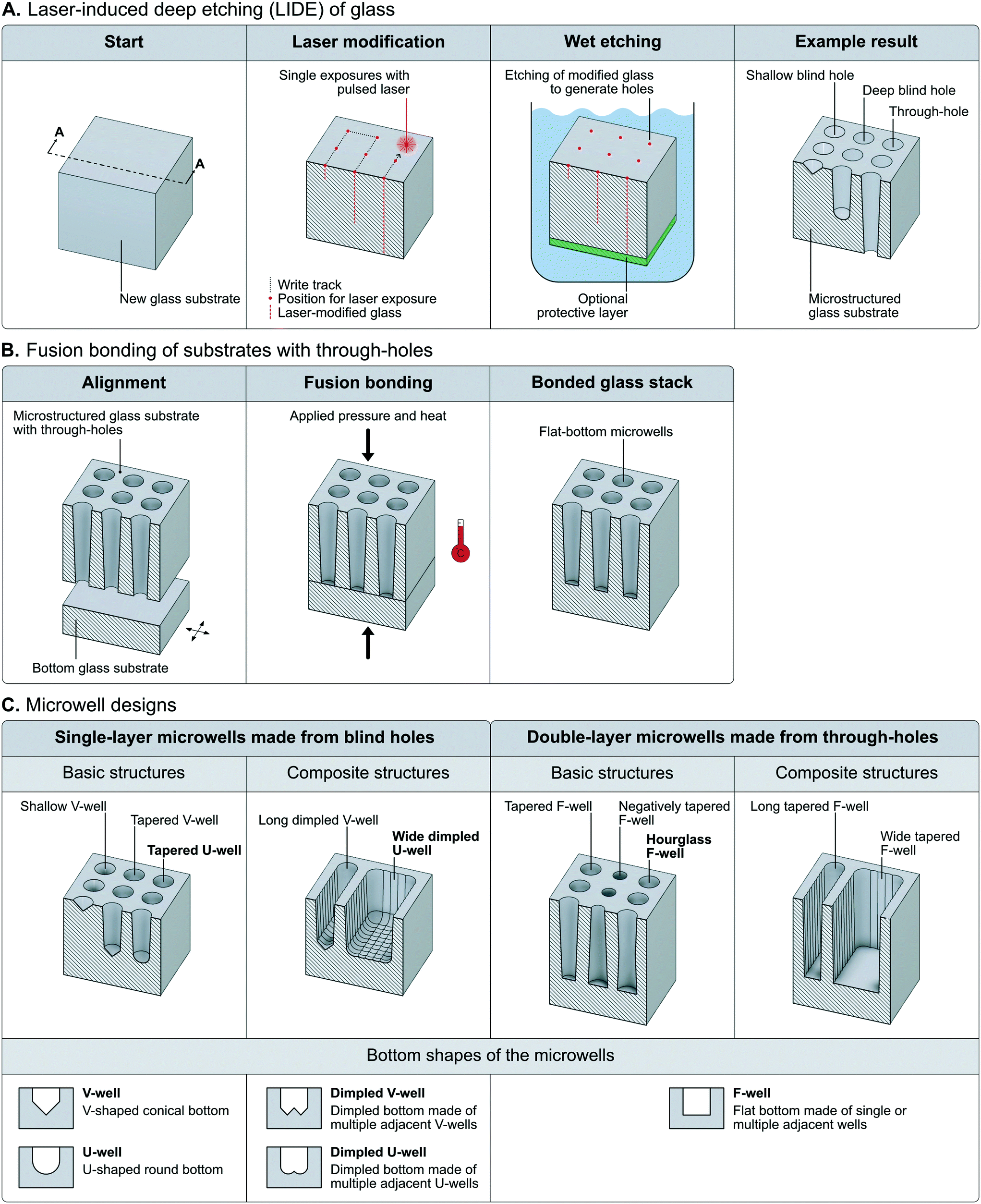 | ||
| Fig. 1 Fabrication scheme of laser-induced deep etching of glass microwells. A) Illustrations of the LIDE-process, including the two main process steps of laser modification of glass and anisotropic wet etching of modified glass, respectively. The process can generate either shallow blind holes, deep blind holes or through-holes of various sizes and shapes. The blind holes can be used directly as microwells for cell assays. B) Illustrations of the fusion bonding process to produce microwells from lide-generated through-holes in glass. C) Examples of microwell designs made of basic (made from one laser exposure) and composite (made from multiple adjacent laser exposures) structures from either single-layer (made from blind-holes) or double-layer (made from through-holes) microwells. The bottom panel illustrates the different bottom shapes of the different types of microwells. The tapered U-well, wide tapered B-well and hourglass F-well (all marked in bold text) were chosen for evaluation in this work. | ||
In the second step, the glass substrate is chemically wet etched. Almost instantly, the modified glass is anisotropically etched, forming deep, micron-sized holes. The remaining unmodified glass is then etched isotropically, widening the already formed hole to a desired width, whereby the etching is stopped. This process enables the fabrication of microwells with an aspect ratio in the order of 1![[thin space (1/6-em)]](https://www.rsc.org/images/entities/char_2009.gif) :10 or more.
:10 or more.
Different types of holes with different taper angles can be generated. The tapering is a result of the declining concentration of etchant further down the hole and depends on the type of glass that is used. As indicated above, it is possible to make shallow or deep “blind holes” that penetrate part of the glass or holes that span the entire thickness of the glass, here called “through-holes”. Through-holes that are etched from both sides have tapered walls giving them an hourglass-shaped profile under standard process conditions. Holes with a positive or negative taper angle can be produced by applying a protective layer on one of the sides before etching, giving them a similar taper profile as for blind holes. Structures that are produced with blind holes are directly suited to be used as microwells for cell assays. They feature either a rounded U-shaped or conical V-shaped bottom profile. To create wells from through-holes, an additional process step to attach a glass wafer that serves as the well bottom is required. Here, this step was done by fusion bonding, which is a technique based on atomic contact between the two glass wafers that is transformed into covalent bonds by applying heat and pressure (Fig. 1B). Fusion bonding provides durability of the bond that is comparable to the bulk material itself. Such double-layer microwells have a flat bottom.
Single holes can be used as building blocks to produce more complex and larger composite structures by simply introducing laser modifications in proximity that can merge during the etching process. Such composite structures can be composed of either blind holes or through-holes to produce grooves of various width and length. The microwell designs that were chosen for evaluation in this work are highlighted with bold text in Fig. 1C.
3. Experimental
3.1 Fabrication of glass microwell array chips
The glass microwell array chips in this work were provided by Arralyze® (LPKF Laser & Electronics AG, Germany). We used BOROFLOAT® 33 (Schott AG), a borosilicate glass that is widely used for life science applications due to low autofluorescence and high optical transparency in the visible region. The 500 μm thick 4′′ wafers that we used had a surface roughness of Ra < 1 nm and warpage/bow of <30 μm, according to the manufacturer's specifications.The LIDE process has been previously described for TGVs elsewhere.39 In short, we first made digital designs of the microwell arrays. They were then used in a commercially available Vitrion S 5000 laser machine (LPKF Laser & Electronics AG, Germany) to define positions of laser exposure. The machine was set to 80% power and local modifications were introduced into the glass wafers by laser exposure in the machine. For through-holes in double-layer glass microwell arrays, the laser focus was positioned in the center of the cross section of the glass wafer. For blind-holes in single-layer glass microwell arrays the focus was lifted upwards until the target hole-depth was archived after etching. Lastly, the glass wafers were wet etched in a diluted HF-solution and the process was monitored until the intended hole-diameter for each type of well was archived.
3.2 Chip assembly for use in inverted microscopes
Glass microwell array chips can be mounted in different types of microscopes and imaging instruments using chip holders. The design of such holders can be adapted for standard formats, such as cell culture dishes or microscope slides, to be able to fit in conventional microscopy stage inserts. In this work, two approaches were used.One approach was based on a previously described holder in the shape of a standard cell culture dish.29 Briefly, the chip was assembled in the bottom part of the circular holder, which had a slot for the chip and an open window underneath for optical access by an inverted microscope. A gasket was magnetically clamped against the perimeter of the chip using a top part, which had a window for topside access to the chip. The window in the top part, together with the gasket, formed a chamber that functioned as a liquid reservoir above the microwell arrays during long term live cell assays. This approach was used with the square-shaped glass chips.
Circular glass chips were instead glued to the bottom of a standard plastic cell culture dish with an outer diameter of 30 mm. The dish had a circular opening in the bottom that was slightly smaller than the glass chip. Before bonding, both the glass chip and the dish were treated with oxygen plasma (Atto-QR-200-PCCE, Diener electronic GmbH + Co. KG) to improve adhesion. Then, adhesive glue (Katiobond OM614, DELO Industrie Klebstoffe GmbH & Co) was dispensed to the plastic dish using a needle valve on an x–y stage. After assembly of the glass chip with the dish, the adhesive was exposed to UV-light with a wavelength of 365 nm for 10 minutes for pre-curing. Lastly, a final thermal curing step was performed at 50 °C for 20 hours. This method produced a mechanically strong and leakage-free bond between the glass chip and the plastic dish. The dish then served as a liquid reservoir on top of the microwell arrays on the glass chip.
In both approaches, a cell culture dish lid was used to cover the liquid reservoir on top of the microwell arrays to prevent evaporation and contamination. The lid was temporarily removed when adding or removing liquids.
3.3 Cells
For the cell assays that were performed in the glass microwell chips, we used human leukemia cell line K562 and human renal cell carcinoma cell line A498 (both from ATCC). We also used the variants K562-GFP and A498-RFP, which expressed green fluorescent protein (GFP) and red fluorescent protein (RFP). K562 was maintained in RPMI 1640 medium supplemented with 10% fetal bovine serum (FBS), 100 U mL−1 penicillin and 100 μg mL−1 streptomycin. A498 and A498-RFP were maintained in DMEM medium supplemented with 10% FBS, 100 U mL−1 penicillin and 100 μg mL−1 streptomycin. Human natural killer (NK) cells were isolated from peripheral blood mononuclear cells (PBMCs) from anonymous healthy donors by negative selection using an NK cell isolation kit (Miltenyi Biotec) and maintained in RPMI 1640 medium supplemented with 10% FBS, 100 U mL−1 penicillin, 100 μg mL−1 streptomycin and 200 U mL−1 of IL-2 (PeproTech) for 3–5 days before experiments. According to local regulations, no ethical permit is needed to use NK cells isolated from anonymous healthy donors.3.4 Cell labelling
Cell lines were transduced to stably express GFP or RFP for long-term proliferation, as previously described.44 For short-term imaging experiments, the cell lines were stained with 1 μM CellTrace Calcein Green AM (Thermo-Fisher Scientific) and/or 2.5 μM CellTrace Far Red (Thermo-Fisher Scientific) viability dyes. For killing assays, NK cells were stained with 0.5 μM CellTrace Yellow (Thermo-Fisher Scientific), target cells with 2.5 μM CellTrace Far Red (Thermo-Fisher Scientific) and cell death was detected by having 1 μM SYTOX Green (Thermo-Fisher Scientific), which leaks in and labels the cell nuclei in dying cells, in the medium during assays. The staining was performed following the manufacturer's protocols.For live cell imaging of actin, A498 cells were detached and transfected with LifeAct-mCherry for 30 min in an Eppendorf tube at 37 °C using Lipofectamine 2000 (Thermo Fisher Scientific) following the manufacturer's protocol and directly plated in the glass microwell chip using complete RPMI medium containing 20000 cells per mL. Cells were left to adhere for 24 hours before imaging. When specified, LifeAct-mCherry-transfected A498 cells were stained with the viability dye Calcein AM. For the microscopy, the medium was replaced by Hanks' balanced salt solution (HBSS, Thermo Fisher Scientific) with 10% FBS.
For actin and tubulin organization over the dimple ridges and 3D reconstruction, 105 RFP-expressing A498 cells were seeded onto the chip and left overnight. The following day, immunofluorescence staining was performed in a light protected environment. The cells were washed three times with PBS, fixed in 4% (w/v) methanol-free formaldehyde (Thermo Fisher Scientific) at room temperature for 15 minutes, washed three times in PBS and then permeabilized with 0.5% Triton-X-100 at room temperature for 5 minutes. The samples were blocked with 5% BSA at room temperature for 5 minutes and incubated with 2 μg mL−1 primary antibody mouse anti tubulin (T6074, Sigma) in PBS at 4 °C overnight. The following day, the cells were washed three times with PBS. The permeabilization and blocking steps were repeated as previously described. The samples were incubated with 2 mg mL−1 goat anti mouse AF647 secondary antibody (A21240, Invitrogen) and 60 nM Oregon Green Phalloidin (07466, Thermo-Fisher) at room temperature for 1 hour. Next, the cells were washed 3 times with PBS and incubated with 2 mg mL−1 DAPI (D1306, Thermo-Fisher) at room temperature for 10 minutes followed by three washing steps with PBS.
3.5 Microscopy
Imaging was performed at 10×, 20× and 63× magnification using a LSM 880 inverted confocal microscope (Zeiss) or an Axio Observer Z1 inverted microscope (Zeiss) with an ORCA-Flash 4.0 camera (Hamamatsu). Both microscopes were equipped with incubation chambers maintained at 37 °C and 5% CO2. Scanning electron microscopy of the glass chips was done on a JSM-6510 (JEOL Ltd.).3.6 Cell imaging
Long term cell cultures (section 4.3), including clonal expansion (section 4.4), were performed by seeding GFP expressing K562 cells in U-wells and F-wells or RFP expressing A498 cells in dimpled U-wells and F-wells. 104-105 cells were seeded onto the chip, resulting in approximately 1–3 cells/well, to give space for the cells to divide. Images of the microwells were acquired every 24 h for 4 days using the Axio Observer Z1 wide field microscope or the LSM 880 confocal microscope, with the microwell chip kept in a CO2 incubator between imaging sessions. A498 cells expressing RFP were used for evaluating cell migration in dimpled U-wells (section 4.6). 105 cells were seeded onto the chip and left to adhere overnight, before imaging every 5 minutes for 12 hours the following day.
The time-lapse live cell imaging of the actin remodelling was conducted using LifeAct-mCherry transfected A498 cells. Images were acquired with a single optical section at 1 frame every 15 seconds using the airyscan detector of the LSM880 microscope (section 4.7). The images were reconstructed using the airyscan processing mode in ZEN (Zeiss). For actin and tubulin organization over the dimple ridges, cells were imaged with the LSM880 confocal microscope (63×, oil) with a z-step of 0.5 μm. For the high-resolution single cell migration assay and actin signal quantification over the dimple ridges, time-lapse imaging of LifeAct-mCherry transfected A498 cells was performed using the LSM880 confocal microscope (63×, oil) with a time frame of 5 minutes.
NK cell cytotoxicity assays were performed by initially seeding activated NK cells and target cell lines onto the chip (section 4.8). When the desired number of NK cells and target cells, i.e., approximately a single NK cell and 3–7 target cells in each well was reached, the surface was rinsed with medium, and the chip was placed under the Axio Observer Z1 wide field microscope acquiring images sequentially at several fields of views every 3 minutes for 12 hours.
3.7 Image analysis
Automatic image analyses of cell proliferation and immune cell cytotoxicity assays were performed using MATLAB (MathWorks, Inc.). Initially, wells were segmented using the bright-field channel. Thresholds were applied to the fluorescent channels followed by a median filter to remove noise and a Gaussian filter to smooth the image. Cells were counted by using a built-in MATLAB algorithm (imregionalmax), detecting regional intensity maxima corresponding to individual cells. Classification of live and dead cells was performed by measuring the SYTOX intensity. Cells were classified as dead if the average SYTOX intensity inside the cell was above a set threshold.Analysis of the positioning of K562 cells inside dimples was performed in MATLAB by fitting a grid with the same size as the dimple structures. The fluorescence image was binarized and cells were segmented using a MATLAB watershed transform (watershed). Each segmented cell was then assigned to the dimple in the grid with maximum overlap and the fraction of the cell inside the dimple was calculated.
Manual image analysis and 3D reconstructions were performed using ImageJ45 and Imaris (Oxford Instruments), respectively. Automatic tracking of migrating A498 cells in dimpled U-wells was performed using the Baxter algorithms.46
4. Results & discussion
Here, we report the first manufacturing, use and biological evaluation of glass microwell array chips made by LIDE in different types of in vitro live cell assays. The evaluation was done by low- and high-resolution microscopy followed by image analysis.4.1 Manufactured glass microwell array chips
The LIDE process was used to manufacture glass microwell array chips with U-wells, dimpled U-wells, and F-wells, as indicated in Fig. 1C. Examples of fabricated chips are shown in Fig. 2. The resulting chips were either 22 mm2 square or circular with a 22 mm diameter. Single-layer chips included multiple arrays with U-wells and dimpled U-wells (Fig. 2A), whereas double-layer chips included a single array with F-wells (Fig. 2B). As described above, circular single-layer chips were glued to the bottom of a 30 mm cell culture dish (Fig. 2C) and square-shaped single-layer or double-layer chips were mounted in a custom-made chip holder (Fig. 2D). | ||
| Fig. 2 Fabricated glass microwell array chips made with LIDE. Photographs of A) a single-layer chip, B) a double-layer chip, C) a circular single-layer chip glued to a culture dish, and D) a square single-layer chip assembled in a chip holder (gasket and lid not included in the photograph). SEM images of E) tapered U-shaped wells in a single-layer chip, F) wide dimpled U-well in a single layer chip, and G) hourglass F-wells in a double layer chip. | ||
The chips were inspected by SEM (Fig. 2E–G), from which it was confirmed that the formed microstructures were free of defects, such as micro-cracks. The rows and columns of microwells in the arrays were distributed with equal pitch between wells and dimples. Both the U-wells and the dimpled U-wells wells had round bottom-shapes whereas the F-wells were flat. The fusion of the glass substrates of the double-layer chips left no visible sign of the previous interface. The U-wells and F-wells both had a top diameter of 90 μm. The F-wells had a bottom diameter of 75 μm, whereas the U-wells had a rounded bottom profile. The dimpled U-wells had a square shape with a width of 1 mm, and individual dimples were 20 μm in width and up to 4 μm in depth (ESI† Fig. S1). The total depths of the inspected microwells were 265 μm for the U wells, 240 μm for the dimpled U-wells, and 405 μm for the F-wells, and the bottom thicknesses were 163 μm, 220 μm and 170 μm, respectively.
4.2 Live cell imaging in different glass microwell designs
First, we evaluated the image quality that could be obtained from inverted light microscopy of fluorescently labelled live cells in the glass microwell chips (Fig. 3A–D). For the intended application of high-content screening with single cell resolution of live cell assays, the minimal requirement was to be able to resolve single cells. For this evaluation, K562 suspension cells and A498 adherent cells were used.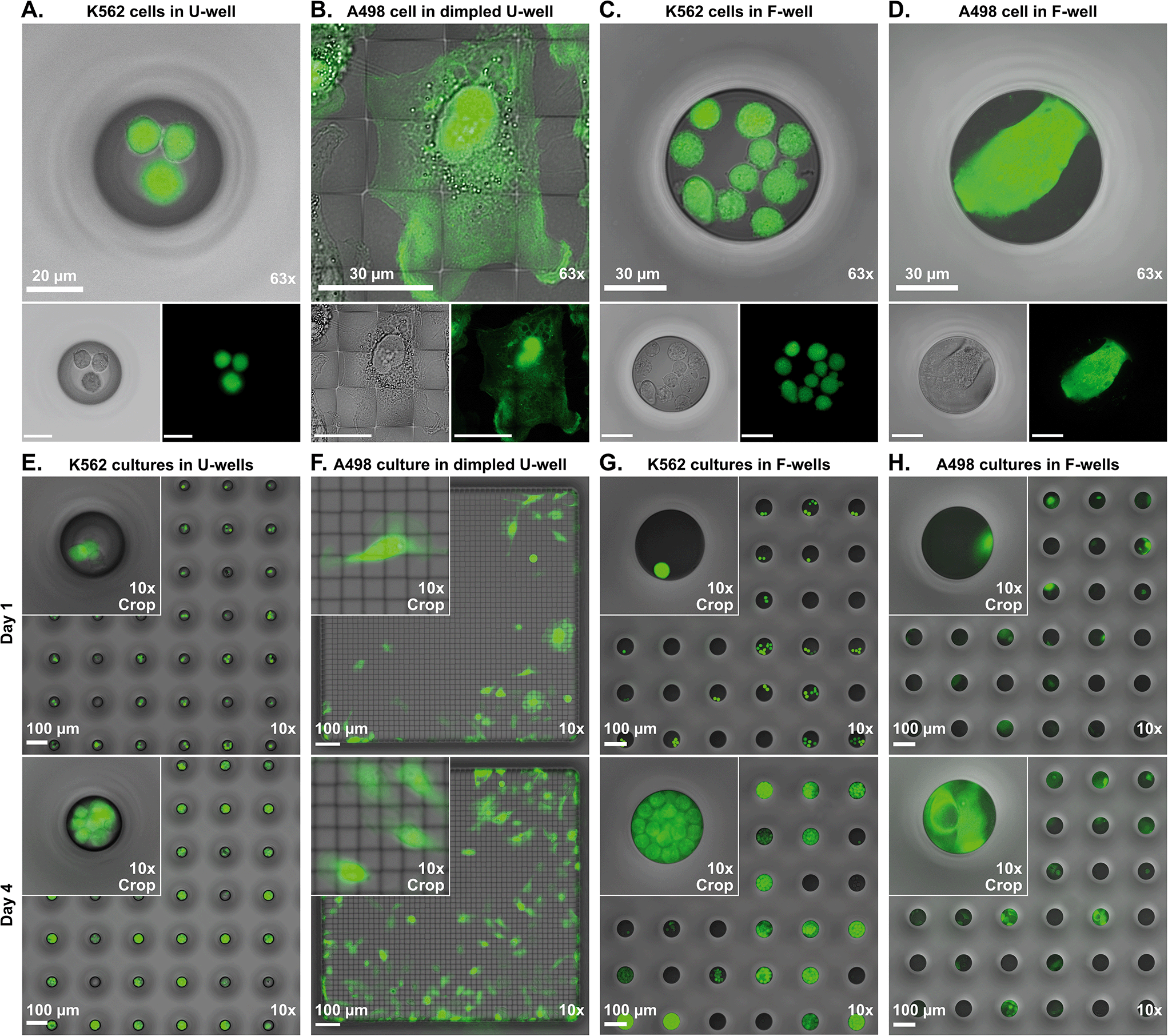 | ||
| Fig. 3 63× high-magnification bright-field and fluorescence imaging of live cells in glass microwells with A) K562 suspension cells in round bottom U-wells in a single-layer chip, B) A498 adherent cells in a dimpled U-well in a single-layer chip, C) K562 suspension cells in a flat bottom F-well in a double-layer chip, and D) A498 adherent cell in a flat bottom F-well in a double-layer chip. Long-term cell culture, showing 10× magnification brightfield and fluorescence images at day 1 (top row) and day 4 (bottom row) of E) K562 cells in U-well array, F) A498 cells in a dimpled U-well, G) K562 cells in an F-well array, and H) A498 cells in an F-well array. | ||
Starting with the U-wells, it was confirmed that single cells could be imaged and distinguished from one another, despite the rounded and light-scattering profile of the well bottom (Fig. 3A). Cells were observed to be in close proximity to one another and could also be located at slightly different heights when several cells occupied a single well.
In the dimpled U-wells, the well floor featured a 3D microstructured landscape. The dimples seemed to have little effect on the image quality, especially compared to U-wells, as even subcellular details were clearly observed (Fig. 3B). In bright-field imaging, the square layout of the dimple ridges was visible in addition to the cell. In fluorescence imaging, the dimples themselves could not be observed but the pattern of the dimple ridges could be discerned by the lack of fluorescence signal from the cell. This observation is further investigated in section 4.7 below.
In contrast to the U wells and dimpled U wells, the flat bottom of the F-wells provided an unobstructed view for imaging of cells. Hence, subcellular detail was clearly visible, even in small suspension cells and image quality was superior to that of U-wells (Fig. 3C). All cells on the well floor could be imaged in one focus plane. In brightfield mode, the exposure was equal across the well floor, in contrast to U-wells, which had a slightly brighter area in the middle of the well.
Lastly, we performed imaging of the larger adherent cells in F-wells. Similarly to the previous results obtained with the smaller suspension cells, we could resolve single cells with subcellular detail (Fig. 3D). However, these cells could stretch over the entire width of the well and adhere to well walls, which could put parts of the cell out of focus.
4.3 Long-term cell cultures in glass microwell arrays
Next, we investigated if LIDE-processed glass of different well shapes and dimensions could support long-term cell cultures. The smaller K562 cells were tested in U-wells and F-wells, whereas the larger A498 cells were tested in F-wells and dimpled U-wells.In all three types of well designs, the cells were cultured successfully for four days (Fig. 3E–H). Viable cell cultures were observed even after seven days; however, the cultures were then expanding out of the smaller wells. In the U-wells and F-wells, the K562 suspension cells were observed to line up in radial patterns as they proliferated. The cells were maintained inside the wells with no sign of escape or accidental transfer of cells between microwells. Wells without cells at the beginning of the assay also remained empty. The larger A498 adherent cells remained viable and proliferated in the small F-wells, but they were observed to migrate on the well walls, making it difficult to set and maintain all cells in focus and consequently to distinguish individual cells. Such events were less of an issue in the large, dimpled U-wells, where the adherent cells could extend and migrate freely while remaining in the same focal plane over the course of the assay. Cell proliferation was similar for A498 cells on both dimpled and flat glass surfaces (ESI† Fig. S2 and Movie S3). The dimpled U-wells also provided the opportunity to follow individual cells over long periods of time, for example to do lineage tracing (ESI† Movie S4).
4.4 Clonal expansion in flat-bottom microwells
The confined microenvironment in the smaller microwells provided a suitable setting for studying the proliferation of single cells over time. Hence, in the following assay, we used F-wells for demonstrating clonal expansion of K562 cells in glass chips.Cells were seeded so that one, two, or three cells occupied each well. Thereafter, the cells were cultured for four days and imaged every day to monitor their proliferation over time (Fig. 4A). Starting with wells having single cells at the beginning of the assay, we observed, on average, a doubling time of 24 hours (Fig. 4B). At day four, different numbers of cells were present in the wells across the arrays (Fig. 4C). Some cells remained viable without dividing successfully, while others proliferated into substantially higher numbers (Fig. 4A), displaying cell heterogeneity in the K562 population. We also investigated if the initial number of cells in the wells affected the proliferation rate (Fig. 4D). The proliferation in wells having one, two or three cells at the beginning of the assay was analyzed. On average, we observed a doubling rate per day in all conditions, however, the wells that housed three cells at the start seemed to have a slightly lower proliferation rate.
 | ||
| Fig. 4 Clonal expansion of K562 suspension cells in F-wells. A) Combined brightfield and fluorescence images of proliferation over 4 days (day 1–4 in columns), where a single cell fails to proliferate (1st row) or successfully proliferates (2nd row), or where two (3rd row) or three (4th row) initial cells proliferate successfully. B) Line plot of the increase of the number of cells per well over the time of the assay, starting with a single cell per well. C) Bar plot showing a histogram of the number of cells present at the end of the assay in the analyzed wells that had a single cell at the start. D) Bar plot showing the number of cells per well at day 2 in wells starting with one, two, or three cells per well. | ||
4.5 Laterally organized cell seeding into dimples
The dimpled U-wells provided a 3D microstructured, egg carton-like floor in the glass. This is similar to previously published work based on conventional wet etching,27 but in contrast, we integrated dimple structures into the bottom of deep microwells. The dimples were designed to specifically fit a single K562 suspension cell. We then investigated whether we could obtain a laterally organized cell seeding on the well floor, where each cell would fall into and occupy its own dimple at predetermined positions.K562 cells were seeded into dimpled U-wells and imaged. Most cells were located alone within, and distributed in the rows and columns of, the dimple structures (Fig. 5A). However, a few cells were also observed to be in contact with, or partly cover, the dimple ridges. The fraction of each cell that was inside the nearest dimple was analyzed by segmenting cells into fractions being inside or outside a dimple (Fig. 5B). The results showed that approximately 60% of the cells had a 90–100% fraction inside a dimple, and the mean fraction inside a dimple of all cells that were analyzed was 88% (Fig. 5C). Thus, the dimples could be used to guide cell seeding into predetermined patterns for a range of different applications and potentially also for making organized monolayers that form cellular networks.
 | ||
| Fig. 5 A) Laterally organized cell seeding of K562 suspension cells into dimples of a dimpled U-well. B) Image segmentation of the fraction of a cell's area that is positioned inside (green) or outside (red) a single dimple (grid overlay representing the dimple ridges), and in C) a bar plot showing a histogram of the results of the image analysis. D) Cell migration in dimpled U-wells of A498 adherent cells, including migration tracks with different colours for different cells, at three different time points: start, middle, end of assay. E) Migration tracks normalized to a starting position of 0,0 (x, y) plotted along the lateral directions of the well. F) Line plot of the migration speed of the tracked cells over the course of the assay. G) Bar plot showing a histogram of the average migration speed. | ||
4.6 Cell migration over 3D dimple microstructures
As observed in the long-term cultures (section 4.3), A498 cells were able to adhere and migrate on the native glass surfaces in the microwells. The dimpled U-wells offered a larger surface area over which the cells could migrate compared to the smaller wells. However, the 3D dimple microstructures presented a different landscape compared to conventional flat cell culture substrates. The dimples were designed to be smaller than the A498 adherent cells, so that the cells would face multiple ridges and dimples at a time rather than a flat surface upon migration.Using the dimpled U-wells, we characterized the A498 cell migration on microstructured glass surfaces. We seeded a low number of cells into dimpled U-wells and monitored the migration over time (Fig. 5D). It was observed that the cells managed to migrate successfully over the dimpled floor of the well. Over the course of the 12 hour assay, the cells migrated long distances in different directions (Fig. 5E). The migration speed varied for all cells but peaked at close to 2 μm min−1 (Fig. 5F). When monitoring a larger set of cells, we observed a mean migration speed of 0.82 μm min−1 (Fig. 5G).
4.7 High-resolution imaging of subcellular protein structures in dimpled U-wells
Performing high-magnification microscopy of subcellular structures requires a cell culture substrate with high optical quality. Glass microwells have great potential for such applications, in particular double-layer chips with F-wells that have a flat #1.5H glass coverslip-like bottom surface. However, the simpler design and manufacturing of single layer microwell chips can potentially provide a lower cost option. As observed in section 4.2, dimpled U-wells showed promising optical quality. In the previous assay presented in section 4.6 above, we observed the migration of A498 cells over dimpled U-wells. In some applications, 3D microstructured surfaces can provide a more in vivo-like topography for contact and migration-focused studies compared to flat cell culture surfaces.47,48 Here, the novel microstructured floor of the dimpled wells combined with high image quality provided a unique opportunity to study subcellular mechanics in detail during migration. Therefore, we further investigated the cell migration in dimpled U-wells by high-magnification confocal and time-lapse microscopy of the actin and tubulin filaments inside the moving cells.First, we did live cell time-lapse imaging of an A498 cell on the dimpled surface during a short time sequence with high time-resolution (Fig. 6A and ESI† Movie S5). Here, we could resolve and observe submicron cellular protrusions containing actin filaments along the cell periphery (Fig. 6B), and in detail see the actin dynamics during retraction and extension (Fig. 6C). We also observed an aggregation of actin close to the cell periphery that was in motion, often in the form of actin puncta. These puncta were localized near the dimple ridges of the glass substrate.
 | ||
| Fig. 6 Confocal imaging at 63× magnification of A498 cells in dimpled U-wells. A) Live-cell airyscan microscopy of an A498 cell transiently transfected with LifeAct-mCherry and acquired for 15 min at 15 s intervals. B) Signal profile along the magenta line as drawn in A). C) Cropped image from the orange box as drawn in A) at different times of the acquisition. White arrows show the cell membrane retraction and extension. Blue arrows show examples of actin filaments withdrawn. Orange arrows show examples of actin puncta formed during the membrane protrusion redeployment. D) An A498-RFP cell was stained for actin, tubulin and nuclei and imaged using confocal microscopy with a z-step of 0.5 μm. The fluorescence images show max projections of the z-stack and three selected optical sections are shown in E) for actin and tubulin, with the focal plane of the dimple ridges used as reference (z = 0 μm). Fluorescence signal is shown down in the dimples, indicating that the cell conforms to the structured glass surface. Signal puncta is visible for actin but not for tubulin along the ridges and above. F) 3D reconstruction of the same A498 cell with a top view (left), a closeup from the orange box (right) and cross section view from the line A–A′ (bottom), showing aggregation of actin, particularly at ridge junctions (arrows), and conformation of the cell membrane along a dimple ridge. Live-cell imaging of a LifeAct-mCherry transfected A498 cell with the brightfield image in G) and the actin signal in H), including measured actin puncta along the dimple ridges. I) The migratory path from multiple time frames of the same cell was tracked manually and the average intensity was projected, showing the area covered by the cell (grey signal) and the migratory path (magenta line). The combined signal from the actin puncta appears as bright lines over the dimple ridges. | ||
We then further analyzed the positioning of an A498 cell on the dimpled surfaces (Fig. 6D). Confocal z-stack imaging indicated that the cells conformed to the shape of the glass. Both actin and tubulin signals were detected below the level of the dimple ridges, however, puncta along the dimple ridges and above could only be seen for actin and not tubulin (Fig. 6E). This was further analyzed by making 3D-projections from the acquired z-stacks, where it was clear that the shape of the cell followed the topology of the microstructured glass surfaces and actin aggregated along the ridge, especially at the junctions of the square-shaped ridge pattern (Fig. 6F).
To further investigate the appearance of actin puncta inside the cells, we performed high resolution time-lapse imaging with longer time intervals of migrating A498 cells over the dimpled surfaces (Fig. 6G and ESI† Movie S6). In single frames of a migrating cell, we could confirm the alignment of the actin puncta with the ridges of the dimple structures in the glass microwell (Fig. 6H). When combining all frames in the sequence into a single image, the square-shaped ridge pattern of the dimples clearly appeared in the fluorescent signal of actin (Fig. 6I). From this time-sequence, the actin now appeared more as lines rather than puncta. This indicated that, during migration, the cell makes contact on multiple positions in proximity along the glass dimple ridges as it moves forward. Apparently, the cell used the 3D microstructures of the glass surface for advancing forward, where the dynamics of the actin filament arrangement was organized and conformed to the microstructured surface. Thus, 3D micro-structuring in glass microwells may enable studying or promoting cell migration over structures of different types of dimple designs, sizes, and densities. It may potentially also enable more detailed investigations of the biomechanics of the acto-myosin network involved in cell migration by high-resolution microscopy.
4.8 Cell cytotoxicity screening in glass microwell arrays
One application where microwells are particularly suitable is immune cell cytotoxicity assays with single cell resolution.11,13,16,17,19,21 Two key aspects are to enable close contact between the immune cells and their targets in a confined space, or to allow for tracking of migration over long distances prior to killing. Here, we investigated how the microwells presented in this work would perform in immune cell cytotoxicity assays.We used primary NK cells as effector cells and K562 cancer cells as targets in the small U-wells and F-wells. After first seeding fluorescently labelled target cells and then effector cells, we performed time-lapse imaging over a period of 6 hours to monitor NK killing of the target cells. We also monitored spontaneous death events of the K562 cells, in wells without NK cells.
Starting with the U-wells, we observed successful NK cell killing (Fig. 7A and ESI† Movie S7). The round and narrow bottom of the wells promoted cell–cell contact but as expected, these types of wells had limited optical quality due to their bottom shape. However, we could still distinguish single cells from one another, especially when looking at the fluorescent signals. It was also possible to readily detect killing events of single cells as the fluorescent signal of the target cells switched from red to green. The number of wells with killed targets was 69% at the end of the assay (Fig. 7B). To enhance the visibility of the cells we made 3D projections of confocal z-stack images of the U-wells (ESI† Movie S8). We could then more clearly distinguish single cells from one another, both laterally and vertically. However, such type of imaging requires more exposures and time to capture each event, which may not be desired for some cytotoxicity screening assays.
 | ||
| Fig. 7 Immune cell cytotoxicity assays in the glass microwell array chips, with cropped images of killing events at three different time points followed by an uncropped image of the last time point. The plots show the accumulated killing over the course of the assays. A and B) NK killing of K562 cells in U-wells. The NK cells were activated with IL-2 for 5 days prior to the assay. C and D) NK killing of K562 cells in flat F-wells. The NK cells were activated with IL-2 for 3 days prior to the assay. E and F) NK killing of A498 cells in dimpled U-wells. The NK cells were activated with IL-2 for 5 days prior to the assay. | ||
In the F-wells, the higher image quality was clearly visible, and it was straightforward to detect and distinguish individual cells and killing events (Fig. 7C and ESI† Movie S9). At the end of the assay, the number of wells with killed targets was 22% (Fig. 7D). Thus, whereas the U-wells promotes cell–cell contacts, the F-wells permits efficient and detailed analysis. Although, the shape difference of the well bottom seemed to lead to higher amount of killing in the U-wells compared to the F-wells, a direct comparison cannot be made since the effector-to-target-cell ratio was not precisely controlled, and the activation of the NK cells was different for the two experiments.
We also evaluated immune cell cytotoxicity assays in the dimpled U-wells wells with NK effector cells and A498 target cells. The optical quality of the microstructured well surface made it easy to detect individual cells and killing events (Fig. 7E and ESI† Movie S10). From the results of section 4.6, we already knew that the large A498 cells were able to migrate over the dimpled microstructures. NK cells, however, are smaller in size than a single dimple. Nevertheless, active NK cells were observed to migrate efficiently over long distances on the microstructured well bottom, whereas less active cells remained inside the dimples. The killing of A498 cells was at first low, as NK cells had not yet reached their first targets (Fig. 7F). After approximately 30 minutes, the killing of targets started and continued throughout the assay. After 6 hours, the fraction of dead target cells was almost 20%.
4.9 Summary of glass microwell arrays for live cell imaging assays
We have evaluated three different types of LIDE-generated microwell designs in single- and double-layer glass chips. Both types of chips and all microwell designs can sustain viable and proliferating cell cultures over multiple days, of both suspension and adherent cell lines. The optical quality of the glass chips allows for high-resolution imaging using either wide-field or confocal microscopy, and detailed analysis of subcellular structures is possible in flat bottom wells but also in 3D microstructured surfaces in single-layer glass chips. All types of tested microwells are suitable for single cell studies, where U-wells provide the tightest confinement for cell clustering and interaction between cells, F-wells provide some freedom of motion but still with proximity between cells, and dimpled U-wells provide more vast space for long-distance migration but where the egg carton-like dimples also can be used for lateral organization of seeded cells. Still, in contrast to conventional multiwell plates, the cells are always confined within the microwells and the imaging field of view, enabling longitudinal studies and accurate tracking over long periods of assay time. The dense microwell arrays on the relatively small chip footprint, also allow for rapid and efficient microscopy screening of a high number of individual cells. Thus, LIDE-manufactured glass microwell array chips may open the possibility for conducting more advanced and up-scaled live cell imaging assays for single cell analysis in the future.4.10 Manufacturing challenges, advantages, and outlook
One characteristic of microwells produced by LIDE is the tapering of the sidewalls, which depends on the type of glass that is used and processing parameters. The tapering is clearly visible in our F-wells and U-wells. Typical taper angles are ≤8°. However, it has been demonstrated that straight side walls can be achieved through optimization for similar processes.43 Another characteristic is rounded bottom profiles in blind holes. This is similar to what is achieved with conventional wet etching of glass,30 but in contrast, the U-wells provide a unique combination of the rounded bottom profile with deep, high-aspect ratio wells, which is difficult to achieve with other methods.Combining U-wells into composite structures can generate large wells, even exceeding microscale dimensions, with novel microstructured bottom surfaces, as demonstrated with the 1 mm wide dimpled U-wells. These surface microstructures can be minimized by reducing the pitch of the laser pulses to achieve near flat surfaces, or further utilized, for example by varying the pitch for making surface microstructure gradients. Currently, it is challenging to achieve a completely flat bottom surface in single glass layer microwells. For that purpose, double-layer designs like our F-wells can be used, resulting in a flat microwell bottom that is optically ideal for high-resolution microscopy.
LIDE offers essential advantages over conventional and state-of-the-art glass microfabrication processes. Each modification is introduced using only a single laser pulse. This minimizes laser-induced stress and defects, such as micro-cracks that are typical for laser ablation of glass. The subsequent etching step completely removes all laser modified glass and any potential laser-induced defects. In this way, defect-free microstructures are generated with native glass material properties, and the mechanical strength remains intact. The combination of high frequency laser pulses with subsequent bulk etching in batches also enables significantly higher throughput than conventional laser ablation or laser-induced selective etching using photosensitive glass, like FLAE or PLAE.
LIDE is a digital technique that does not require physical masks or other layout specific tools for each new design, so both prototyping and high-volume manufacturing is cost-efficient. It is also versatile as it can be used for both small and large structures going only partially or all the way through the substrate. The type of glass can be selected based on requirements of the application, instead of requirements of the fabrication method, and cell compatible and low-cost materials are widely available. Thus, LIDE can be explored for new types of glass microwell array designs for life sciences and may also enable a seamless translation of academic research to healthcare and commercial applications.
5. Conclusions
With this work, we have introduced LIDE as a glass microfabrication technique for producing microwell array glass chips. We have demonstrated microwells with unique well designs and evaluated them in several live cell imaging assays. LIDE enables the realization of miniaturized devices in pure glass with a range of possible designs and 3D microstructured surfaces that can be tailored for different types of usages. The simplicity, versatility, and high quality in manufacturing make such glass devices, especially microwell array chips, suitable for a range of applications, stretching from cell line development, drug development and screening to diagnostics and precision medicine.Author contributions
N. S., M. S.-R., R. A. K., and B. Ö. contributed to the conceptualization of the work. The methodology was developed by N. S., L. B., P. A. S., C. Z., K. G., B. R., R. A. K., and B. Ö., whereas the investigation, data curation, and formal analysis was done by L. B., P. A. S., C. Z., and B. R. The project was administrated by N. S., R. A. K., and B. Ö., and the supervision was done by N. S. and B. Ö. Visualization was conducted by N. S., L. B., P. A. S., and C. Z. The writing of the original draft was done by N. S., R. A. K., and B. Ö., with help from L. B., P. A. S., C. Z., and M. S.-R., whereas the review and editing was done by N. S. with help from P. A. S., C. Z., R. A. K., and B. Ö.Conflicts of interest
The LIDE technology is proprietary and is commercialized for cell experiments under the brand ARRALYZE® by LPKF Laser & Electronics AG. The authors B. R., M. S. R. and R. A. K. are employees of LPKF Laser & Electronics AG.Acknowledgements
The LifeAct-mCherry was a kind gift of Gisou van der Goot. We would also like to thank Nora Fekete-Drimusz for valuable discussions and proof reading of the manuscript.References
- M. Mattiazzi Usaj, C. H. L. Yeung, H. Friesen, C. Boone and B. J. Andrews, Cell Syst., 2021, 12, 608–621 CrossRef CAS PubMed.
- H. Axelsson, H. Almqvist, M. Otrocka, M. Vallin, S. Lundqvist, P. Hansson, U. Karlsson, T. Lundbäck and B. Seashore-Ludlow, ACS Chem. Biol., 2018, 13, 942–950 CrossRef CAS PubMed.
- Y. German, L. Vulliard, A. Kamnev, L. Pfajfer, J. Huemer, A. K. Mautner, A. Rubio, A. Kalinichenko, K. Boztug, A. Ferrand, J. Menche and L. Dupré, Cell Rep., 2021, 36, 109318 CrossRef CAS PubMed.
- R. Clark, L. Usselmann, M. R. Brown, A. U. Goeppert and A. Corrigan, J. Immunol. Methods, 2019, 473, 112636 CrossRef CAS PubMed.
- L. Albertí-Servera, S. Demeyer, I. Govaerts, T. Swings, J. De Bie, O. Gielen, M. Brociner, L. Michaux, J. Maertens, A. Uyttebroeck, K. De Keersmaecker, N. Boeckx, H. Segers and J. Cools, Blood, 2021, 137, 801–811 CrossRef PubMed.
- X. Xing, F. Yang, Q. Huang, H. Guo, J. Li, M. Qiu, F. Bai and J. Wang, Sci. Adv., 2021, 7, 9738–9765 CrossRef PubMed.
- J. S. Duprez, M. Cohen, S. Li, D. Wilson, R. H. Brookes and D. A. James, J. Immunol. Methods, 2021, 495, 113083 CrossRef CAS PubMed.
- C. Maucourant, I. Filipovic, A. Ponzetta, S. Aleman, M. Cornillet, L. Hertwig, B. Strunz, A. Lentini, B. Reinius, D. Brownlie, A. Cuapio, E. H. Ask, R. M. Hull, A. Haroun-Izquierdo, M. Schaffer, J. Klingström, E. Folkesson, M. Buggert, J. K. Sandberg, L. I. Eriksson, O. Rooyackers, H. G. Ljunggren, K. J. Malmberg, J. Michaëlsson, N. Marquardt, Q. Hammer, K. Strålin and N. K. Björkström, Sci. Immunol., 2020, 5, 6832 CrossRef PubMed.
- ANSI/SLAS 1–2004: Microplates — Footprint Dimensions.
- S. Lindström and H. Andersson-Svahn, Biochim. Biophys. Acta, Gen. Subj., 2011, 1810, 308–316 CrossRef PubMed.
- I. N. Bandey, J. R. T. Adolacion, G. Romain, M. M. Paniagua, X. An, A. Saeedi, I. Liadi, Z. You, R. B. Rajanayake, P. Hwu, H. Singh, L. J. Cooper and N. Varadarajan, J. ImmunoTher. Cancer, 2021, 9, e001877 CrossRef PubMed.
- S.-E. Kim, H. Kim and J. Doh, Lab Chip, 2019, 19, 2009–2018 RSC.
- I. Prager, C. Liesche, H. van Ooijen, D. Urlaub, Q. Verron, N. Sandström, F. Fasbender, M. Claus, R. Eils, J. Beaudouin, B. Önfelt and C. Watzl, J. Exp. Med., 2019, 216, 2113–2127 CrossRef CAS PubMed.
- A. Desalvo, F. Bateman, E. James, H. Morgan and T. Elliott, Lab Chip, 2020, 20, 3772–3783 RSC.
- A. Ogunniyi, C. M. Story, E. Papa, E. Guillen and J. C. Love, Nat. Protoc., 2009, 45, 767–782 CrossRef PubMed.
- N. Varadarajan, B. Julg, Y. J. Yamanaka, H. Chen, A. O. Ogunniyi, E. McAndrew, L. C. Porter, A. Piechocka-Trocha, B. J. Hill, D. C. Douek, F. Pereyra, B. D. Walker and J. C. Love, J. Clin. Invest., 2011, 121, 4322–4331 CrossRef CAS PubMed.
- K. Guldevall, L. Brandt, E. Forslund, K. Olofsson, T. W. Frisk, P. E. Olofsson, K. Gustafsson, O. Manneberg, B. Vanherberghen, H. Brismar, K. Kärre, M. Uhlin and B. Önfelt, Front. Immunol., 2016, 7, 24 Search PubMed.
- Y. Zhou, N. Shao, R. Bessa de Castro, P. Zhang, Y. Ma, X. Liu, F. Huang, R.-F. F. Wang and L. Qin, Cell Rep., 2020, 31, 107574 CrossRef CAS PubMed.
- E. Forslund, K. Guldevall, P. E. Olofsson, T. Frisk, A. E. Christakou, M. Wiklund and B. Önfelt, Front. Immunol., 2012, 3, 300 Search PubMed.
- W. Yang, H. Yu, G. Li, F. Wei, Y. Wang and L. Liu, Lab Chip, 2017, 17, 4243–4252 RSC.
- T. W. Frisk, M. A. Khorshidi, K. Guldevall, B. Vanherberghen and B. Önfelt, Biomed. Microdevices, 2011, 13, 683–693 CrossRef PubMed.
- C.-K. Huang, G. J. Paylaga, S. Bupphathong and K.-H. Lin, Biofabrication, 2020, 12, 025016 CrossRef CAS PubMed.
- A. A. Manzoor, L. Romita and D. K. Hwang, Can. J. Chem. Eng., 2021, 99, 61–96 CrossRef CAS.
- E. Gencturk, S. Mutlu and K. O. Ulgen, Biomicrofluidics, 2017, 11, 051502 CrossRef PubMed.
- S.-S. D. Carter, A.-R. Atif, S. Kadekar, I. Lanekoff, H. Engqvist, O. P. Varghese, M. Tenje and G. Mestres, Organs-on-a-Chip, 2020, 2, 100004 CrossRef.
- A. Shakeri, S. Khan and T. F. Didar, Lab Chip, 2021, 21, 3053–3075 RSC.
- M. Deutsch, A. Deutsch, O. Shirihai, I. Hurevich, E. Afrimzon, Y. Shafran and N. Zurgil, Lab Chip, 2006, 6, 995 RSC.
- Y. Guan and W. Kisaalita, Colloids Surf., B, 2011, 84, 35–43 CrossRef CAS PubMed.
- T. W. Molter, S. C. McQuaide, M. T. Suchorolski, T. J. Strovas, L. W. Burgess, D. R. Meldrum and M. E. Lidstrom, Sens. Actuators, B, 2009, 135, 678–686 CrossRef CAS PubMed.
- H. Zhu, M. Holl, T. Ray, S. Bhushan and D. R. Meldrum, J. Micromech. Microeng., 2009, 19, 065013 CrossRef.
- L. A. Hof and J. A. Ziki, Micromachines, 2017, 8, 53 CrossRef.
- T. Tang, Y. Yuan, Y. Yalikun, Y. Hosokawa, M. Li and Y. Tanaka, Sens. Actuators, B, 2021, 339, 129859 CrossRef CAS.
- M. P. Jahan, A. Perveen and A. M. Rumsey, Mach. Sci. Technol., 2019, 23, 264–338 CrossRef.
- K. Sugioka, J. Xu, D. Wu, Y. Hanada, Z. Wang, Y. Cheng and K. Midorikawa, Lab Chip, 2014, 14, 3447–3458 RSC.
- F. Sima, K. Sugioka, R. M. Vázquez, R. Osellame, L. Kelemen and P. Ormos, NANO, 2018, 7, 613–634 CAS.
- F. Jipa, S. Orobeti, C. Butnaru, M. Zamfirescu, E. Axente, F. Sima and K. Sugioka, Appl. Sci., 2020, 10, 8947 CrossRef CAS.
- F. Jipa, S. Iosub, B. Calin, E. Axente, F. Sima and K. Sugioka, Nanomaterials, 2018, 8, 583 CrossRef PubMed.
- F. Sima, H. Kawano, M. Hirano, A. Miyawaki, K. Obata, D. Serien and K. Sugioka, Adv. Mater. Technol., 2020, 5, 2000484 CrossRef CAS.
- R. Ostholt, N. Ambrosius and R. A. Krüger, in Proceedings of the 5th Electronics System-integration Technology Conference (ESTC), IEEE, 2014, pp. 1–3 Search PubMed.
- R. A. Krüger, N. Ambrosius and R. Ostholt, DPMA, DE102013103370A1, 2013.
- N. Ambrosius and R. Ostholt, DPMA, DE102014113339A1, 2014.
- R. Ostholt, N. Ambrosius, D. Dunker and A. Schnoor, WIPO, WO2018210484A1, 2017.
- L. Chen and D. Yu, J. Mater. Sci.: Mater. Electron., 2021, 32, 16481–16493 CrossRef CAS.
- S. J. Edwards, V. Carannante, K. Kuhnigk, H. Ring, T. Tararuk, F. Hallböök, H. Blom, B. Önfelt and H. Brismar, Front. Mol. Biosci., 2020, 7, 208 CrossRef CAS PubMed.
- W. S. Rasband, ImageJ, U. S. National Institutes of Health, Bethesda, Maryland, USA, 1997–2018, https://imagej.nih.gov/ij/ Search PubMed.
- K. E. G. Magnusson, J. Jalden, P. M. Gilbert and H. M. Blau, IEEE Trans. Med. Imaging, 2015, 34, 911–929 Search PubMed.
- M. Ermis, E. Antmen and V. Hasirci, Bioact. Mater., 2018, 3, 355–369 CrossRef PubMed.
- C. De Pascalis and S. Etienne-Manneville, Mol. Biol. Cell, 2017, 28, 1833–1846 CrossRef CAS PubMed.
Footnote |
| † Electronic supplementary information (ESI) available: S1. Figure of surface profile measurements of a dimpled U-well. S2. Figure of A498 cell proliferation on flat vs. dimpled glass surfaces. S3. Movie of A498 cell proliferation on flat vs. dimpled glass surfaces. S4. Movie of A498 cell culture in a dimpled U-well with lineage tracing. S5. Movie of A498 cell membrane retraction and redeployment on a dimpled U-well. S6. Movie of A498 cell migration on a dimpled surface, with the formation of actin puncta on dimple ridges. S7. Movie of cytotoxicity assay with NK cells killing K562 cells in a U-well. S8. Movie of a 3D reconstruction of confocal z-stack images of NK cells + K562 cells in a U-well. S9. Movie of a cytotoxicity assay with NK cells killing K562 cells in an F-well. S10. Movie of a cytotoxicity assay with NK cells killing A498 cells in a dimpled U-well. See DOI: https://10.1039/d2lc00090c |
| This journal is © The Royal Society of Chemistry 2022 |