
Spatial trans-epithelial electrical resistance (S-TEER) integrated in organs-on-chips†
Noa
Renous‡
a,
Mark D.
Kiri‡
a,
Ronny A.
Barnea
b,
Rossana
Rauti
 a,
Yael
Leichtmann-Bardoogo
a and
Ben M.
Maoz
*acd
a,
Yael
Leichtmann-Bardoogo
a and
Ben M.
Maoz
*acd
aDepartment of Biomedical Engineering, Tel Aviv University, Tel Aviv 69978, Israel. E-mail: bmaoz@tauex.tau.ac.il
bSchool of Chemistry, Sackler Faculty of Exact Sciences, Tel Aviv University, Tel Aviv 69978, Israel
cSagol School of Neuroscience, Tel Aviv University, Tel Aviv 69978, Israel
dThe Center of Nanoscience and Nanotechnology, Tel Aviv University, Tel Aviv 69978, Israel
First published on 22nd November 2021
Abstract
Transepithelial/transendothelial electrical resistance (TEER) is a label-free assay that is commonly used to assess tissue barrier integrity. TEER measurement systems have been embedded in organ-on-a-chip devices to provide live readouts of barrier functionality. Yet, these systems commonly provide the impedance values which correspond to the highest level of permeability throughout the chip and cannot provide localized information on specific regions of interest. This work introduces a system that provides this essential information: a spatial-TEER (S-TEER) organ-on-a-chip platform, which incorporates moving (scanning) electrodes that can measure electrical resistance at any desired location along the chip. We demonstrate the system's capacity to obtain localized measurements of permeability in selected regions of a cell sample. We show how, in a layer with non-uniform levels of cell coverage, permeability is higher in areas with lower cell density—suggesting that the system can be used to monitor local cellular growth in vitro. To demonstrate the applicability of the chip in studies of barrier function, we characterize tissue response to TNF-α and to EGTA, agents known to harm tissue barrier integrity.
Introduction
Organs-on-chips are microfluidic devices that serve as in vitro models to mimic tissue and organ-like physiology.1 A key benefit that organs-on-chips provide over traditional in vitro cell models is the capacity to incorporate perfusion through microchannels, which is an essential function in physiological modelling and in drug screening applications.2The increasing prevalence of organs-on-chips in in vitro modeling has created a need for technology that provides real-time readouts of cell function within these systems. One fundamental type of measurement is the permeability of cell-layers within a chip; such measurements can indicate the functionality of barrier tissues such as those found in the lungs,3 gut,4 blood brain barrier (BBB),5–7 and vasculature (endothelium). Fluorescent markers are one common method of measuring permeability.8 Another common method is impedance measurement,9i.e., measurement of electrical resistance across a cellular monolayer. The latter method, known as transepithelial or transendothelial electrical resistance (TEER), provides label-free, rapid, and real-time measurements that correlate to the formation of tight junctions between the cells in the monolayer, thereby providing a good indication of barrier integrity.
In recent years, several methods have been developed to integrate TEER into organ-on-chip systems. These methods include: direct insertion of metal electrodes into designated placeholders10–15—either in individual chips or in high-throughput systems containing multiple chips,15 patterned electrodes on glass or polymeric substrate,16–19 or integrated electrodes with other sensors such as multi electrode arrays (MEA).20 While these methods of TEER integration provide in situ information on barrier function, most of them do not capture spatial information, meaning that they cannot indicate electrical resistance values in specific parts of the chip. Rather, they provide the electrical resistance value corresponding to the highest level of permeability, i.e., the “weakest link in the chain”.21 This feature may result in substantial loss of information: for example, a tissue might be confluent with good tight junctions, yet contain small imperfections that ultimately provide very low TEER values, which do not represent the overall sample.22 Some state-of-the-art chips overcome this limitation to some degree by integrating multiple electrodes, which can be used to capture electrical resistance in specific spatial locations inside a channel of a microfluidic chip.20,23 Yet, these locations must be chosen in advance, meaning that the technology cannot be used to identify multiple locations of interest in real time and to compare their TEER measurements. The capacity to dynamically combine TEER measurements with spatial information could enable researchers to obtain valuable information that is currently beyond the scope of TEER measurement methods. Such information might include, for example, the influence of flow shear stress gradient,24 drug diffusion loss,25 effects of local oxygen concentrations,26 and more.
Currently, microscopy is the primary means of retrieving spatial information in organs-on-chips,27,28 yet it is challenging to correlate microscopy data with permeability measurements. Thus far, most attempts to measure spatial permeability in vitro—e.g., through conductance scanning methods—have focused on non-organ-on-chip systems.29,30 One study proposed the use of multiple patterned electrodes to obtain spatial information on impedance in a microfluidic BBB model; however, the electrodes are complex to fabricate, partially interfere with cell culture visualization (unless additional steps are taken that may further complicate fabrication), and have not yet been demonstrated in vitro.31
In this work, we introduce an organ-on-a-chip platform integrated with moving (scanning) electrodes, designed and fabricated so as to provide a dynamic range of measurement points throughout the organ-on-a-chip channel. We demonstrate this new concept of spatial-TEER (S-TEER) by characterizing the growth dynamic of human epithelial colorectal adenocarcinoma (Caco-2) cells in a chip and measuring cell response to two different agents known to decrease barrier integrity: TNF-α, a pro-inflammatory cytokine;20 and EGTA, a chelating agent that impairs barrier function of cells.17
Materials and methods
Chip fabrication
The developed S-TEER-Chip is a multilayer microfluidic device consisting of the following components (Fig. 1 and SI1, Movie SI1†): (i) three polydimethylsiloxane (PDMS) substrates: a top layer and two fluidic layers, or “channels” (referred to, respectively, as the “upper channel” and “lower channel”); (ii) one bottom glass layer containing two static patterned gold electrodes, integrated with the lower channel; (iii) two stainless steel electrodes, integrated with the upper channel, and with the capacity to move along (“scan”) a designated slot spanning the length of the channel; and (iv) a porous polycarbonate (PC) membrane between the PDMS channels (Fig. 1). Chip fabrication included several steps: electrode fabrication; PDMS layer fabrication; and assembly. | ||
| Fig. 1 S-TEER chip design. a. Photograph of the assembled chip, scale bar – 5 mm. b. CAD model – middle cut of S-TEER chip c. exploded CAD model of the S-TEER chip. Gold-plated electrodes on the glass coverslip and stainless-steel electrodes with 2 mm tip inside the channel. PDMS layers made from 3D-printed molds. d. Illustration of the impedance measurement inside the system – 2 excitation electrodes and 2 sensing electrodes. The chip dimensions provided in the “Materials and method” section and in Fig. SI1.† | ||
![[thin space (1/6-em)]](https://www.rsc.org/images/entities/char_2009.gif) :10 ratio Sylgard 184® (Dow Corning, Midland, MI, USA) with the curing agent, followed by vacuum for 1 hour and curing at 60 °C for 4 hours.
:10 ratio Sylgard 184® (Dow Corning, Midland, MI, USA) with the curing agent, followed by vacuum for 1 hour and curing at 60 °C for 4 hours.
In order to avoid the formation of bubbles, all the channels were filled with medium. Using this method enabled us to have flow in the chip without bubble formation for long time periods (Movie SI2†).
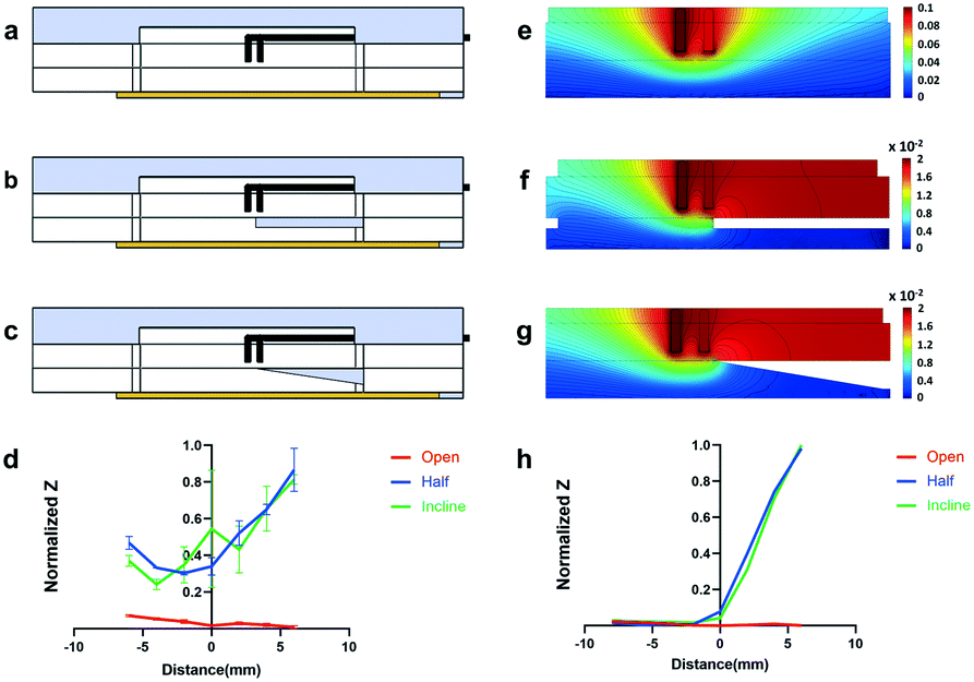 | ||
| Fig. 2 Chip characterization. a–c. Illustration of three chip configurations: (a) open-Chip, (b) half-open chip, and (c) incline-chip. d. Impedance measurements through the channel, showing the spatial measurement distribution in the three chips. e–g. Electrical potential distribution in the three chips, (e) open-chip, (f) half-open chip, and (g) incline-chip. h. Impedance simulations throughout the channel, showing spatial measurement distributions in the three chips. | ||
Chip cell culture
Caco-2 cells (ATCC® HBT-37™, American Type Culture Collection, Rockville, MD, USA) were maintained in Dulbecco's modified Eagle medium (DMEM, Biological Industries), supplemented with 10% heat-inactivated fetal bovine serum (FBS, Biological Industries), 1% glutamax (Gibco), and 1% penicillin–streptomycin–amphotericin B (PSA, Biological Industries) solution, at 37 °C with 5% CO2 in a humidifying incubator. Cells of early passages20–30 were grown to 80–90% confluency before being seeded into the microfluidic device. The chip was pretreated on plasma for 1 minute, followed by flushing with ethanol and phosphate-buffered saline (PBS), then coated with Matrigel Basement Membrane Matrix (Corning) used at a 1:50 ratio with the culture medium, for 30 min in the incubator. The membrane was then rinsed with culture medium, and the Caco-2 cells, harvested with trypsin/EDTA solution (Biological Industries), were seeded in the upper channel on top of the PC membrane, at a density of 1 × 10⁶ cells per cm2, and cultured statically, changing the medium twice a day.
Non-confluent layers: the non-confluent layer was created in several methods, which include: 1. uneven seeding density (seeding more cells on one side of the chip then the other), 2. inducing shear in the channel right after seeding.
Immunocytochemistry
Chips were rinsed in PBS and fixed in 4% paraformaldehyde (PFA, Sigma-Aldrich) for 20 minutes at room temperature (RT). Immunocytochemistry was carried out after permeabilization with 0.1% Triton X-100 (Sigma-Aldrich) in PBS for 10 min at RT and blocking for 30 min in FBS (5%) in PBS. Primary antibodies were applied overnight in PBS at 4 °C. The primary antibody that was used was rabbit anti ZO-1(Abcam) diluted 1:200 in PBS to stain the zona occludens-1. Cells were then washed three times in PBS and stained with the secondary antibody for 1 hour at RT. The secondary antibody was anti-rabbit Alexa Fluor-488 (Invitrogen) diluted 1:300 in PBS. After four washes with PBS, DAPI-fluoromount-G® (SouthernBiotech) was mounted to stain the nuclei as well. Imaging was carried out using an inverted confocal microscope (Olympus FV3000-IX83). To retrieve complete images of each channel, we used sequential tile scanning over the entire channel. Reconstruction and processing were done using open-source ImageJ software.32
Impedance spectroscopy measurements
Electrode sterilization: the electrodes were placed in UV-O for 5 minutes. In addition, the electrodes were washed with 70% ethanol.A BioLogic potentiostat (VSP) was used to record impedance spectra. Measurements were executed by applying a 10 μA sinusoidal excitation signal in a 4 point measuring system with a frequency range of 1 Hz–1 MHz.
In experiments involving chips containing cells, S-TEER-chips were transferred one at a time from the incubator, and the measurements were taken shortly after at 4 different points within each chip. Measurement of a full impedance spectrum requires about 1 minute, and measurement at each point was repeated 4 times.
To ensure consistency in the measurement positions within and across chips, we used a caliper that was connected to the electrode. This provided accuracy of ±10 μm (Movie SI35†).
Simulations
In order to better understand the viability of the proposed system, as well as to support or challenge any experimental results, simulations of the electrical behavior of the S-TEER device were conducted using COMSOL Multiphysics® software (COMSOL Multiphysics® http://www.comsol.com/ COMSOL AB, Stockholm, Sweden). The finite-element-method-based simulations included calculation of the electrostatic field distribution for all versions of the device, in multiple configurations (the different configurations are elaborated above and in the Results section; see cross sections in Fig. 2), and for all locations of the scanning electrodes along the upper channel. The physics model used in COMSOL was “Electric Currents”. Electrical impedance was calculated through extraction of the appropriate currents and voltage drops from frequency-domain simulations of the electrical currents problem (in the frequency range 1 Hz–1 MHz), performed using a flexible generalized-minimum-residual iterative solver.Quantifying cell coverage in a channel
To quantify cell coverage in a chip, we obtained a confocal image of the chip and opened it in ImageJ. The image was converted to greyscale, and thresholding was used to identify the cells inside the chip. We split the image into equal-sized regions of interest (ROIs), with each ROI covering the entire width of the chip. We then measured the “area fraction” of an ROI: assuming that a confluent area of cells inside the channel is 100% coverage, the other areas' values were normalized accordingly.Barrier disruption experiments
641) (Fig. SI8†). TEER was measured using a Millicell ERS-2 Voltohmmeter (Merck Millipore).
The TEER measurements were correlated with microscope images.
Statistical analysis
Results are presented as mean ± SD. Differences between measurement sites in the chip were evaluated using multiple-comparison ANOVA (GraphPad Prism 9.1.0), with P < 0.05 indicating a statistically significant difference between points.Results and discussion
S-TEER-chip design
The S-TEER-chip contains four integrated electrodes: two moving (scanning) electrodes in the upper channel, with a fixed distance between them; and two static electrodes in the lower channel, where the channels are separated by a PC membrane (Fig. 1 and SI1 and Movie SI1†). Each pair of electrodes in each channel contains one excitation electrode (injecting the current) and one sensing electrode (measuring the voltage drop). The scanning electrodes are positioned within a slot spanning the length of the upper channel, and can be moved manually to any desired point along that slot, in order to measure the local impedance at that site (the electrodes are held in place while measurements are taken). This design provides a dynamic range of impedance measurements throughout the organ-on-a-chip system. In designing the device, we encountered and overcame several challenges. The main obstacle was the dependence of impedance measurements on the distance between the moving and static electrodes. In our initial designs, the static electrodes were in the center of the chip, and we observed that the greater the distance between the moving (scanning) electrodes (top) and the fixed electrodes (bottom), the higher the impedance (Fig. SI2†), as the impedance is directly proportional to the distance. To overcome this challenge, we designed the bottom electrodes so as to cover the entire channel (Fig. 1), thereby ensuring identical distance between the top and bottom electrodes at every point in the chip and enabling direct comparisons to be made among all measurement points (Fig. SI3†).Yet, this design created a new challenge, since covering the entire channel with metal electrodes interferes with the capacity to image the cells in the chip, which is fundamental for any organ-on-a-chip application. We overcame this challenge by making the electrodes transparent, by depositing a thin 20 nm layer of gold, as described in Henry et al.17
The choice to use four electrodes (two moving in the upper channel and two static in the lower channel) rather than, e.g., one moving electrode and one static electrode, was driven by considerations regarding the electrode polarization impedance. Specifically, previous work17,23,33 has demonstrated the importance of using a 4-point measuring system instead of 2 points, as a 4-point system enables the excitation electrode to be separated from the measuring electrode. Importantly, the two top electrodes are able to move together, remaining at a constant distance. This is extremely important, as both our experiments and our simulations (Fig. SI4 and SI5†) showed that if one of the upper electrodes is fixed, the impedance is affected.
Summing up the above, our final design eliminates impedance dependence on the distance between the electrodes, allows for cell imaging, and mitigates concerns regarding electrode polarization impedance.
We note that, for the purposes of our proof of concept, we used stainless steel to construct the scanning electrodes and gold for the static electrodes. In real-world applications, alternative metals can be used that are optimal for the experimental conditions and for preserving cell viability. Moreover, we manufactured our chips using standard tools (not photolithography) to facilitate faster and cheaper fabrication; standard micro and nano fabrication methods can be used to miniaturize the chip. It is also important to note that the choice of materials for the membrane may impose downstream constraints; for example, in our case, the use of a PC membrane required additional staining in order to better characterize the cells as bright-field or phase-contrast imaging was more challenging.
Chip characterization
In order to characterize and validate the S-TEER-chip, we created three different chip configurations, containing different resistance layers of PDMS: (i) an open-chip (Fig. 2a), in which there is no barrier between the upper and lower channels; (ii) a half-open-chip (Fig. 2b), which is divided in such a way that half of the chip has an added resistance layer of 0.5 mm of PDMS between the channels, while the other half remains open; and (iii) an incline-chip (Fig. 2c), in which the lower channel includes a layer of PDMS that increases in thickness from one end of the chip to the other, from 0 up to 1.5 mm. We produced and studied three chips in each configuration.Spatial TEER measurements in a cell layer
Once the S-TEER-chip was characterized, we sought to demonstrate its potential as an in vitro platform by identifying changes in tight junctions of barrier tissues. Therefore, we conducted several experiments in which we seeded human epithelial colorectal adenocarcinoma cells (Caco-2 cells) inside the upper channel on top of the PC membrane. In all experiments, TEER measurements were taken at least three times at 4 consistent points throughout the channel, about 5 minutes after taking the chip out of the incubator. The triple measurement, as well as the waiting period before measurements were conducted, mitigated the likelihood that the TEER measurements would be influenced by fluctuations in the medium temperature.9 | ||
| Fig. 3 Spatial TEER measurements. a. Confocal image of Caco-2 cells in a confluent channel (blue-DAPI, Green ZO-1). b. Magnified images of specific points on a confluent chip: (i) 1, (ii) 2, (iii) 3, (iv) 4. c. Normalized impedance values at 4 points on a confluent channel. d. Correlation between the percentage of cell coverage in the channel and the impedance value at the same point. e. Normalized impedance values in 4 points of a non-confluent channel. (f) Magnified images of specific points on a non-confluent chip: (i) 1, (ii) 2, (iii) 3, (iv) 4. (g) Confocal image of Caco-2 cells in a non-confluent channel (*P < 0.05, **P < 0.01, ***P < 0.001). | ||
 | ||
| Fig. 4 EGTA effect on Caco-2 in the S-TEER chip. a. Confocal image of a confluent layer of Caco-2 in S-TEER chip. Nuclei stained in blue and ZO-1 in green. b. DIC images of Caco-2 in different stages of the experiment; (i) control chip w/o EGTA; (ii) under EGTA effect; (iii) after 1 day of recovery. c. TEER values over different time points – control over cells treated with 5 mM of EGTA solution. | ||
As a next step, we quantified the correspondence between TEER values and the percentage of cell coverage at each measurement site (Fig. 3d). It can be seen that when cell coverage is below 50% the impedance values are low (<0.4). This trend was observed in all the chips that were used in this study.
These measurements provide an indication of the valuable information that S-TEER can capture. For example, they show how our system can be used to obtain localized measurements of a tissue barrier within a sample, providing fine-grained structural information. This capacity can contribute to the accuracy of interpretation of TEER data. Indeed, it is common for the distribution of cells in a channel to be uneven (e.g., Fig. 3f and g), and for distributions to vary across experiments, owing to slight variations in parameters and execution techniques. In these cases, areas with lower cell coverage may produce low TEER values that are not necessarily representative of the entire cell layer (as shown, e.g., in Fig. 3d–g). Traditional TEER methods, which are heavily influenced by the “weakest link” in the sample in terms of permeability,21 may thus not produce an accurate picture of the permeability of the complete sample.
The capacity to provide an accurate assessment of permeability in specific areas of a sample might further allow for the use of chips that might otherwise be discarded as “bad samples”. Fig. 3d suggests, for example, that a region of the cellular layer with coverage lower than 50% is characterized by low impedance values that might disqualify a sample. The capacity to focus measurements on areas with higher cell coverage might enable samples that contain sparse regions to be used nonetheless.
Our experiments further suggest that S-TEER might be used to track the growth dynamics of a cellular layer and to measure increases in tissue thickness or confluency at any site in the microfluidic device (Fig. SI6a†). Currently, in most experiments, cellular growth in a chip is monitored via microscope, which does not provide a means of quantifying how permeability properties change over time. S-TEER, in contrast, can be used to monitor different points in the chip over time, and to measure how the confluency and permeability change in situ. Such information can be combined with microscopy data—with either bright field or immunohistochemistry—to obtain a complete characterization of the growth dynamics.
Using S-TEER to characterize barrier functionality
To demonstrate the capacity of the S-TEER-chip to indicate barrier functionality, we monitored changes in permeability due to exposure to two reagents: the cytokine TNF-α (Fig. SI7b†), and the chelating agent EGTA (Fig. 4b and c and SI8†), which are known to damage barrier integrity.As expected, after introduction of EGTA, we observed a decrease in the impedance at each measurement point (Fig. 4c). Moreover, we observed that the impedance values varied slightly across the different measurement points, indicating that the effects of the agents on the tissue were not completely uniform, and highlighting the capacity of the S-TEER chip to provide nuanced structural information. The recovery was not complete, and as shown in differential interference contrast (DIC) images on the channel (Fig. 4b), was similar to the confluency 2 days before the measurement.
The findings of our barrier functionality experiments highlight another advantage provided by the S-TEER system. In many dual-channel organ-on-a-chip platforms, including the system described herein, it is challenging to obtain images at high magnification, owing to the relatively large distance between the cell layer and the bottom of the chip. This characteristic makes it difficult to visualize barrier breakdowns, as disintegration of tight junctions can be hard to see at low magnifications. S-TEER measurements can circumvent this limitation by identifying local effects on barrier tissue.
Conclusions
Herein we have introduced the S-TEER-chip, an organ-on-a-chip platform that provides localized impedance measurements at multiple points along a chip. Our system relies on a 4-point measuring system, using a pair of static transparent electrodes and a pair of scanning electrodes that can be moved manually along the chip to obtain impedance measurements at a site of interest. We validated our system in experiments using Caco-2 cells, showing that the S-TEER-chip platform produces spatially-dependent impedance measurements that are in direct correlation with cell concentration levels in the corresponding areas on the chip. We further demonstrated how the S-TEER system can be used to monitor spatial dynamics of cellular growth, and to identify changes in barrier integrity following exposure to either TNF-α or EGTA.The S-TEER-chip system provides substantial benefits over current TEER measurement approaches, which rely on lowest values of electrical resistance across the entire channel and cannot provide an indication of local variations along the cellular layer. In enabling researchers to retrieve such spatial information, our platform can provide more accurate measurements and open the door to spatially dependent studies. Furthermore, in contrast to standard TEER approaches, which require full cellular confluence to produce accurate measurements, our approach may enable researchers to use chips that contain areas that are not confluent (and to focus on the confluent areas)—potentially saving time and money.
Conflicts of interest
There are no conflicts to declare.Acknowledgements
This research was supported by the Azrieli Foundation, Israel Science Foundation 2248/19, ERC SweetBrain 851765. The authors would also like to thank Dr. Oliver Y. F. Henry, Prof. Yossi Shacham-Diamand and Kian Kadan for fruitful discussions, and Mr. Baptiste Le-Roi for his assistance with the artwork.Notes and references
- S. N. Bhatia and D. E. Ingber, Microfluidic organs-on-chips, Nat. Biotechnol., 2014, 32(8), 760–772 CrossRef CAS.
- D. T. T. Phan, X. Wang, A. Sobrino, D. Zhao, J. C. Chen and L. Y. N. Lee, et al., A vascularized and perfused organ-on-a-chip platform for large-scale drug screening applications, Lab Chip, 2017, 17(3), 511–520 RSC.
- D. Huh, B. D. Matthews, A. Mammoto, M. Montoya-Zavala, H. Y. Hsin and D. E. Ingber, Reconstituting Organ-Level Lung Functions on a Chip, Science, 2010, 328(5986), 1662–1668 CrossRef CAS.
- S. Jalili-Firoozinezhad, F. S. Gazzaniga, E. L. Calamari, D. M. Camacho, C. W. Fadel and A. Bein, et al., A complex human gut microbiome cultured in an anaerobic intestine-on-a-chip, Nat. Biomed. Eng., 2019, 3(7), 520–531 CrossRef CAS.
- G. Adriani, D. Ma, A. Pavesi, R. D. Kamm and E. L. K. Goh, A 3D neurovascular microfluidic model consisting of neurons, astrocytes and cerebral endothelial cells as a blood–brain barrier, Lab Chip, 2017, 17(3), 448–459 RSC.
- B. M. Maoz, A. Herland, E. A. FitzGerald, T. Grevesse, C. Vidoudez and A. R. Pacheco, et al., A linked organ-on-chip model of the human neurovascular unit reveals the metabolic coupling of endothelial and neuronal cells, Nat. Biotechnol., 2018, 36(9), 865–874 CrossRef CAS PubMed.
- C. Hajal, B. Le Roi, R. D. Kamm and B. M. Maoz, Biology and Models of the Blood Brain Barrier, Annu. Rev. Biomed. Eng., 2021, 23, 359–384 CrossRef CAS PubMed.
- M. Martins-Green, M. Petreaca and M. Yao, An Assay System for In Vitro Detection of Permeability in Human “Endothelium.”, in Methods in Enzymology, Elsevier, 2008, ch. 8, pp. 137–53, Available from: https://linkinghub.elsevier.com/retrieve/pii/S0076687908020089 Search PubMed.
- B. Srinivasan, A. R. Kolli, M. B. Esch, H. E. Abaci, M. L. Shuler and J. J. Hickman, TEER Measurement Techniques for In Vitro Barrier Model Systems, J. Lab. Autom., 2015, 20(2), 107–126 CrossRef CAS.
- Y. I. Wang, H. E. Abaci and M. L. Shuler, Microfluidic blood-brain barrier model provides in vivo-like barrier properties for drug permeability screening: Microfluidic BBB Model Mimics In Vivo Properties, Biotechnol. Bioeng., 2017, 114(1), 184–194 CrossRef CAS PubMed.
- N. J. Douville, Y.-C. Tung, R. Li, J. D. Wang, M. E. H. El-Sayed and S. Takayama, Fabrication of Two-Layered Channel System with Embedded Electrodes to Measure Resistance Across Epithelial and Endothelial Barriers, Anal. Chem., 2010, 82(6), 2505–2511 CrossRef CAS.
- Q. Ramadan and F. C. W. Ting, In vitro micro-physiological immune-competent model of the human skin, Lab Chip, 2016, 16(10), 1899–1908 RSC.
- M. W. van der Helm, M. Odijk, J.-P. Frimat, A. D. van der Meer, J. C. T. Eijkel and A. van den Berg, et al., Direct quantification of transendothelial electrical resistance in organs-on-chips, Biosens. Bioelectron., 2016, 85, 924–929 CrossRef CAS PubMed.
- G. Linz, S. B. Rauer, Y. Kuhn, S. Wennemaring, L. Siedler and S. Singh, et al., 3D-Printed Bioreactor with Integrated Impedance Spectroscopy for Cell Barrier Monitoring, Adv. Mater. Technol., 2021, 6(6), 2100009 CrossRef CAS.
- A. Nicolas, F. Schavemaker, K. Kosim, D. Kurek, M. Haarmans and M. Bulst, et al., High throughput transepithelial electrical resistance (TEER) measurements on perfused membrane-free epithelia, Lab Chip, 2021, 21(9), 1676–1685 RSC.
- R. Booth and H. Kim, Characterization of a microfluidic in vitro model of the blood-brain barrier (μBBB), Lab Chip, 2012, 12(10), 1784 RSC.
- O. Y. F. Henry, R. Villenave, M. J. Cronce, W. D. Leineweber, M. A. Benz and D. E. Ingber, Organs-on-chips with integrated electrodes for trans-epithelial electrical resistance (TEER) measurements of human epithelial barrier function, Lab Chip, 2017, 17(13), 2264–2271 RSC.
- S. Deinhardt-Emmer, K. Rennert, E. Schicke, Z. Cseresnyés, M. Windolph and S. Nietzsche, et al., Co-infection with Staphylococcus aureus after primary influenza virus infection leads to damage of the endothelium in a human alveolus-on-a-chip model, Biofabrication, 2020, 12(2), 025012 CrossRef CAS PubMed.
- M. A. U. Khalid, Y. S. Kim, M. Ali, B. G. Lee, Y.-J. Cho and K. H. Choi, A lung cancer-on-chip platform with integrated biosensors for physiological monitoring and toxicity assessment, Biochem. Eng. J., 2020, 155, 107469 CrossRef CAS.
- B. M. Maoz, A. Herland, O. Y. F. Henry, W. D. Leineweber, M. Yadid and J. Doyle, et al., Organs-on-Chips with combined multi-electrode array and transepithelial electrical resistance measurement capabilities, Lab Chip, 2017, 17(13), 2294–2302 RSC.
- M. Odijk, A. D. van der Meer, D. Levner, H. J. Kim, M. W. van der Helm and L. I. Segerink, et al., Measuring direct current trans-epithelial electrical resistance in organ-on-a-chip microsystems, Lab Chip, 2015, 15(3), 745–752 RSC.
- J. Yeste, X. Illa, C. Gutiérrez, M. Solé, A. Guimerà and R. Villa, Geometric correction factor for transepithelial electrical resistance measurements in transwell and microfluidic cell cultures, J. Phys. D: Appl. Phys., 2016, 49(37), 375401 CrossRef.
- M. W. van der Helm, O. Y. F. Henry, A. Bein, T. Hamkins-Indik, M. J. Cronce and W. D. Leineweber, et al., Non-invasive sensing of transepithelial barrier function and tissue differentiation in organs-on-chips using impedance spectroscopy, Lab Chip, 2019, 19(3), 452–463 RSC.
- N. Sakamoto, N. Saito, X. Han, T. Ohashi and M. Sato, Effect of spatial gradient in fluid shear stress on morphological changes in endothelial cells in response to flow, Biochem. Biophys. Res. Commun., 2010, 395(2), 264–269 CrossRef CAS PubMed.
- V. S. Shirure and S. C. George, Design considerations to minimize the impact of drug absorption in polymer-based organ-on-a-chip platforms, Lab Chip, 2017, 17(4), 681–690 RSC.
- Y. B. Arık, M. W. van der Helm, M. Odijk, L. I. Segerink, R. Passier and A. van den Berg, et al., Barriers-on-chips: Measurement of barrier function of tissues in organs-on-chips, Biomicrofluidics, 2018, 12(4), 042218 CrossRef PubMed.
- Z. Li, W. Su, Y. Zhu, T. Tao, D. Li and X. Peng, et al., Drug absorption related nephrotoxicity assessment on an intestine-kidney chip, Biomicrofluidics, 2017, 11(3), 034114 CrossRef PubMed.
- J. A. Brown, V. Pensabene, D. A. Markov, V. Allwardt, M. D. Neely and M. Shi, et al., Recreating blood-brain barrier physiology and structure on chip: A novel neurovascular microfluidic bioreactor, Biomicrofluidics, 2015, 9(5), 054124 CrossRef PubMed.
- M. Fromm, S. M. Krug, S. Zeissig, J. F. Richter, R. Rosenthal and J.-D. Schulzke, et al., High-Resolution Analysis of Barrier Function, Ann. N. Y. Acad. Sci., 2009, 1165(1), 74–81 CrossRef CAS.
- A. H. Gitter, F. Wullstein, M. Fromm and J. D. Schulzke, Epithelial barrier defects in ulcerative colitis: Characterization and quantification by electrophysiological imaging, Gastroenterology, 2001, 121(6), 1320–1328 CrossRef CAS.
- J. Yeste, X. Illa, A. Guimerà and R. Villa, in A novel strategy to monitor microfluidic in-vitro blood-brain barrier models using impedance spectroscopy, ed. S. van den Driesche, Barcelona, Spain, 2015, p. 95180N, Available from: http://proceedings.spiedigitallibrary.org/proceeding.aspx?doi=10.1117/12.<?ccdc_no 2180567?>2180567<?ccdc END?> Search PubMed.
- C. A. Schneider, W. S. Rasband and K. W. Eliceiri, NIH Image to ImageJ: 25 years of image analysis, Nat. Methods, 2012, 9(7), 671–675 CrossRef CAS PubMed.
- T. K. Bera, Bioelectrical Impedance Methods for Noninvasive Health Monitoring: A Review, J. Med. Eng., 2014, 2014, 1–28 CrossRef.
Footnotes |
| † Electronic supplementary information (ESI) available. See DOI: 10.1039/d1lc00789k |
| ‡ Author are equal contributors. |
| This journal is © The Royal Society of Chemistry 2022 |