 Open Access Article
 This Open Access Article is licensed under a
 Creative Commons Attribution 3.0 Unported Licence
Ex situ Ge-doping of CZTS nanocrystals and CZTSSe solar absorber films
Matthew C.
Naylor
 a,
Devendra
Tiwari
ab,
Alice
Sheppard
b,
Jude
Laverock
c,
Stephen
Campbell
a,
Bethan
Ford
a,
Xinya
Xu
a,
Michael D. K.
Jones
a,
Yongtao
Qu
a,
Pietro
Maiello
a,
Vincent
Barrioz
a,
Neil S.
Beattie
a,
Neil A.
Fox
bc,
David J.
Fermin
b and
Guillaume
Zoppi
*a
a,
Devendra
Tiwari
ab,
Alice
Sheppard
b,
Jude
Laverock
c,
Stephen
Campbell
a,
Bethan
Ford
a,
Xinya
Xu
a,
Michael D. K.
Jones
a,
Yongtao
Qu
a,
Pietro
Maiello
a,
Vincent
Barrioz
a,
Neil S.
Beattie
a,
Neil A.
Fox
bc,
David J.
Fermin
b and
Guillaume
Zoppi
*a
aDepartment of Mathematics, Physics and Electrical Engineering, Northumbria University, Ellison Building, Newcastle Upon Tyne, NE1 8ST, UK. E-mail: guillaume.zoppi@northumbria.ac.uk
bSchool of Chemistry, University of Bristol, Cantock’s close, Bristol, BS8 1TS, UK
cH.H. Wills Physics Laboratory, University of Bristol, Tyndall Av., Bristol, BS8 1TL, UK
First published on 13th July 2022
Abstract
Cu2ZnSn(S,Se)4 (CZTSSe) is a promising material for thin-film photovoltaics, however, the open-circuit voltage (VOC) deficit of CZTSSe prevents the device performance from exceeding 13% conversion efficiency. CZTSSe is a heavily compensated material that is rich in point defects and prone to the formation of secondary phases. The landscape of these defects is complex and some mitigation is possible by employing non-stoichiometric conditions. Another route used to reduce the effects of undesirable defects is the doping and alloying of the material to suppress certain defects and improve crystallization, such as with germanium. The majority of works deposit Ge adjacent to a stacked metallic precursor deposited by physical vapour deposition before annealing in a selenium rich atmosphere. Here, we use an established hot-injection process to synthesise Cu2ZnSnS4 nanocrystals of a pre-determined composition, which are subsequently doped with Ge during selenisation to aid recrystallisation and reduce the effects of Sn species. Through Ge incorporation, we demonstrate structural changes with a negligible change in the energy bandgap but substantial increases in the crystallinity and grain morphology, which are associated with a Ge–Se growth mechanism, and gains in both the VOC and conversion efficiency. We use surface energy-filtered photoelectron emission microscopy (EF-PEEM) to map the surface work function terrains and show an improved electronic landscape, which we attribute to a reduction in the segregation of low local effective work function (LEWF) Sn(II) chalcogenide phases.
Introduction
Cu2ZnSn(S,Se)4 (CZTSSe) is a promising material for thin-film photovoltaics whose core constituent elements are Earth abundant and non-toxic. CZTSSe is an attractive material due to its close relation to the commercially-established Cu(In,Ga)Se2 photovoltaic technology and, thus, the potential for knowledge transfer between analogues. The open-circuit (VOC) deficit of CZTSSe devices is severe and prevents the device performance from exceeding conversion efficiencies of ∼12.7%.1,2 A large portion of this deficit is associated with atomic disorder in the lattice, giving rise to a complicated landscape of point defects and the problematic coupling of defects or so-called defect complexes.3 The current understanding in the literature surmises that a Cu-poor and Zn-rich stoichiometry can suppress the formation of some point defects and secondary phases, but alas, the potent VOC deficit is still observed.4 Sn-related defects, namely the SnZn antisite defect, have been identified as being particularly detrimental through the facilitation of mid-band charge carrier recombination sites, which pin the VOC to sub-energy bandgap (Eg) potentials.5,6 The multivalency of Sn permits different valences of the SnZn antisite defects and as such, SnZn2+ and SnZn4+ coexist. The coupling of SnZn2+ with the abundant CuZn+ antisite defect forms the cluster [SnZn2+ + 2CuZn+], which has been reported to cause band-tailing and further restricts the VOC.7 One method to change the electric properties of CZTSSe is to alloy or extrinsically dope the material; elements such as Ag,8 Cd,9 Ge10,11 and Sb12,13 have been used to moderate success. It is important to distinguish between doping and alloying when studying these mechanisms as the former involves nominal quantities in an effort to affect the electronic properties, whereas the latter involves significantly greater quantities which fundamentally change the electronic and structural identity of the compound – this distinction has been comprehensively reviewed in the literature.14Considering the potential origins of the VOC deficit, Sn sites are a clear target for doping and alloying, and Ge emerges as an obvious candidate due to elemental grouping. Ge incorporation, despite its elemental cost and abundance, remains a fruitful platform to investigate electronic effects which could later be reproduced by alternative means once further understood. Ge has consistently proven to result in enhanced device performance, namely the VOC, with the majority of studies probing the effects of Ge on bulk recombination pathways.10,11,15–19 Although, to fully understand the role that Ge plays in improving the device performance and, in particular, VOC losses, here, for the first time, we analyse the surfaces of CZTSSe films with Ge doping with energy-filtered photoelectron emission microscopy (EF-PEEM) to map the surface work function terrains. This would provide insights into the possible recombination prevalent at the CZTSSe/CdS interface and the physico-chemical mechanism of Ge’s role in reducing these shunting pathways.
To date, the majority of Ge doping studies have used a sacrificial Ge layer to dope a metallic precursor stack deposited by vacuum-based techniques10,16,18 or have used a chemical route to introduce significant quantities of Ge during or prior to the formation of Cu2ZnSnS4 (CZTS) compounds, also referred to as in situ doping or alloying.11,20 In this study, we introduce Ge independently to the formation of CZTS, via the so-called ex situ route, to decouple the effects of Ge from those of premature phases (binary and ternary chalcogenides) and investigate the effect of Ge doping on the transition from CZTS to CZTSSe. To achieve this ex situ doping effect, we unusually combine solution and physical vapour deposition techniques such that solution processed quaternary CZTS precursors are combined with elemental Ge films using a separate vacuum-based deposition step. This approach somewhat isolates the doping mechanisms, which allows this work to probe the enhanced grain growth, Ge–Sn interactions and the suppression of Sn disorder at a Sn-rich CZTSSe/CdS interface in a new light.
Results and discussions
CZTS crystalline nanoparticles, known herein has as nanocrystals (NCs), were synthesised using a hot-injection method and re-dispersed to form a NC-based ink.21 Slot-die coating was used to deposit the NC based-ink and form the quaternary precursor layer; a thickness of 800 nm was achieved by successive coatings with an intermediate soft-baking step of the films at 300 °C in air. The precursor films were then selenised and annealed under an Se–Ar2 atmosphere at 500 °C for 20 minutes. Ge was incorporated by the electron beam evaporation of an elemental Ge underlayer 5, 15 and 50 nm prior to CZTS precursor deposition. Accordingly, the samples are labelled as ‘CZTSSe’, ‘Ge5:CZTSSe’, ‘Ge15:CZTSSe’ and ‘Ge50:CZTSSe’ for CZTSSe films with no Ge, and with 5 nm, 15 nm and 50 nm of Ge underlayer, respectively. Other strategies of incorporating the Ge into the CZTSSe layer were also explored, including the addition of Ge layers after the precursor deposition step, which upon selenisation led to a graded Ge profile with dominant distribution limited to the CZTSSe front surface. Thus, this suggests the poor incorporation of Ge and perhaps the volatilisation of Ge–chalcogenide phases (GexSey) during annealing, which are known to have low melting points relative to those of other metallic phases22 – notably similar at a Se-rich stoichiometry to the renowned SnxSey species.23 However, the addition of Ge as an underlayer to the CZTSSe films results in the retention of nominal Ge concentration in the films. Fig. 1a shows the elemental depth profile of Ge across the thickness of the precursor CZTS films overlaid on a cross-section micrograph, which demonstrates that the Ge distribution remains concentrated at the Mo/CZTS interface after successive soft baking steps. Fig. 1b shows the secondary ion mass spectroscopy (SIMS) depth profiles of Ge across the CZTSSe devices, along with Cu and Mo as indicators of the Mo/CZTSSe structure, for undoped and 50 nm Ge underlayer. It is clear that upon selenisation, Ge diffuses homogeneously over the entire CZTSSe film. Considering the absorber thickness of 1 μm, a 5 nm Ge underlayer will correspond to a nominal doping equivalent to 0.06 atomic% and, similarly, 15 nm and 50 nm Ge will be equivalent to 0.18% atomic% and 0.6 atomic%, respectively. The solar cell devices were completed in a substrate architecture with a SLG/Mo/(Ge)/CZTSSe/CdS/i-ZnO/ITO/Ni–Al structure. Further details of the sample preparation are available in the Experimental section.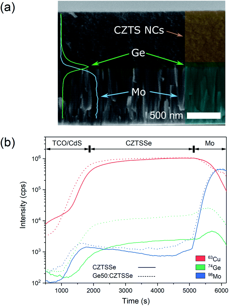 | ||
| Fig. 1 (a) Elemental depth-profile of Ge and Mo acquired through an EDS lines scan overlaid onto a cross-sectional scanning electron micrograph of a CZTS precursor film. (b) SIMS depth profile of Ge, along with Cu and Mo, indicating the construction of the TCO/CZTS/Mo structure upon annealing for CZTSSe and Ge50:CZTSSe. | ||
Fig. 2 depicts the structural properties of selenised CZTSSe and Ge:CZTSSe films probed by X-ray diffraction (XRD). The XRD patterns (Fig. 2a) are consistent with the formation of the pure kesterite phase (I-4). No additional peaks due to secondary phases are visible, confirming the phase-purity of the films. Comparison of the observed XRD patterns with the Bragg reflections of the ICDD standards for kesterite Cu2ZnSnS4 and Cu2ZnSnSe4 suggests a nearly complete selenisation of the CZTS precursor films. The addition of Ge to CZTSSe systematically shifts the peak positions of the Sn dominated planes to larger angles, see Fig. 2b for the (002) example, while the planes without Sn show only marginal changes. This is indicative of Ge substitution at isoelectronic Sn-sites within the lattice. Furthermore, the peaks undergo a relative increase in intensity of 66%, 168% and 224% for the Ge5:CZTSSe, Ge15:CZTSSe and Ge50:CZTSSe films, respectively, compared to those of the CZTSSe films, as well as a narrowing of peak widths, which means improved crystallisation with Ge incorporation. Consequently, the average crystallite sizes in the CZTSSe, Ge5:CZTSSe, Ge15:CZTSSe and Ge50:CZTSSe films calculated using the Scherrer equation from the (002) peaks (Fig. 2c) increase from 40 to 88 nm. The scanning electron microscopy (SEM) cross-sectional images of CZTSSe and Ge50:CZTSSe solar devices (Fig. 3) evidence a significant increase in grain sizes from <1 μm to >1 μm laterally and a grain structure spanning across the thickness of the absorber upon doping. Consequently, the enlarged grain sizes can qualitatively be correlated to an increased surface roughness through inspection of the transparent conducting oxide (TCO) layer’s morphology, shown in the upper section of the micrographs (Fig. 3).
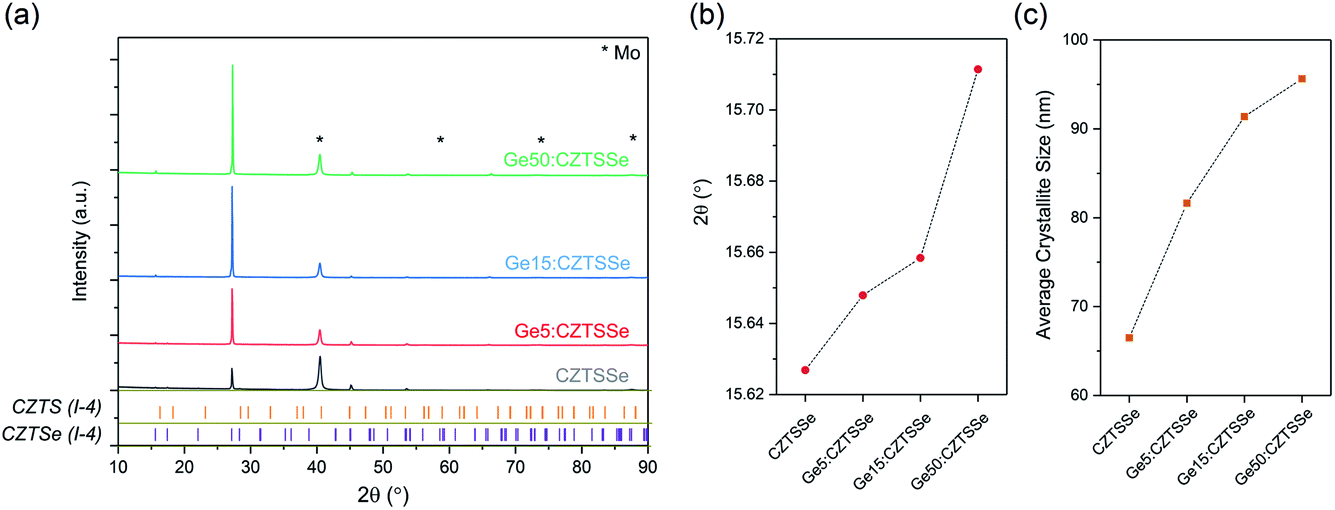 | ||
| Fig. 2 (a) Structural analysis of CZTSSe films using XRD. XRD patterns of CZTSSe films with or without Ge along with the Bragg reflections of kesterite (I-4) Cu2ZnSnS4 and Cu2ZnSnSe4. (b) 2θ shift of the (002) peak and (c) average crystallite sizes of (002) orientation CZTSSe films with respect to the Ge amount. | ||
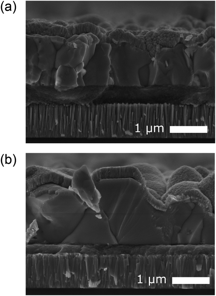 | ||
| Fig. 3 Cross-sectional scanning electron micrograph of a complete solar cell device (SLG/Mo/(Ge)CZTSSe/CdS/i-ZnO/ITO) fabricating using (a) no Ge doping and (b) a 50 nm Ge underlayer. | ||
The phase purity of CZTSSe films was also corroborated with Raman spectroscopy (Fig. 4a), with all films displaying A-symmetry modes at around 174 cm−1, 179 cm−1 and 199 cm−1 associated with the kesterite phase. Comparing the observed Raman shifts to those reported for CZTS–Se solid mixtures suggests the nearly complete selenisation of the precursor CZTS films. No other peaks due to secondary phases were detected using the 633 nm excitation wavelength. Ge doping, especially Ge50:CZTSSe, results in a blue-shift of about 1 cm−1 relative to the CZTSSe films, as has been previously reported, and confirms the inclusion of Ge in the CZTSSe lattice18 (Fig. 4b). Additionally, Ge addition to the CZTSSe films results in an increased asymmetry of the peaks (Fig. 4b), which has been associated previously with the degree of disorder in Ge:CZTSSe prepared by sputtering absorbers.
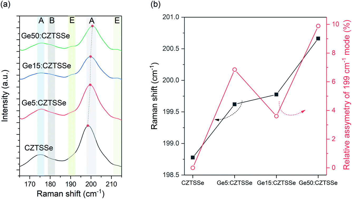 | ||
| Fig. 4 (a). Raman spectra of CZTSSe films with or without Ge under 633 nm excitation. (b) Relative shift and asymmetry of the 199 cm−1 peak measured for the CZTSSe films with and without Ge. | ||
The elemental atomic ratios of Sn(Ge)/(Cu + Zn + Sn), Cu/(Zn + Sn) and Se/(S + Se) derived from quantitative energy dispersive X-ray spectroscopy (EDS) are presented in Fig. 5. Cu/(Zn + Sn) and Se/(S + Se) remain confined closely to 0.813 ± 0.008 and 0.963 ± 0.018, respectively, thus confirming a nearly selenised stoichiometry. Interestingly, the Sn concentration decreases systematically with Ge addition to the films, thus suggesting Ge substitution on Sn atoms in the lattice during annealing. In contrast to the bulk, the surface composition of the CZTSSe films measured by X-ray photoelectron spectroscopy (XPS) analysis determined Zn/Sn and Cu/(Zn + Sn) ratios of 0.360 and 0.848 for CZTSSe and 0.466 and 0.763 for Ge5:CZTSSe, respectively, indicating a significantly Zn-poor surface composition. Additionally, Se/(S + Se) ratios of 0.735 and 0.715 for CZTSSe and Ge5:CZTSSe, respectively, suggest a more sulphur rich composition than that of the bulk of 22% compared to 4%. These contrasting stoichiometries at the film surface to that of the bulk would crucially govern the interfacial properties and, thus, the work function landscape and device performance.
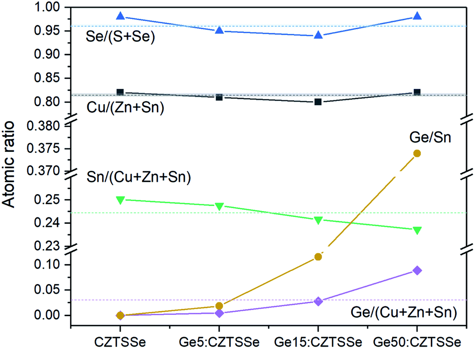 | ||
| Fig. 5 Variation in bulk atomic ratios for CZTSSe films with and without Ge doping, calculated from quantitative EDS measurements. | ||
Fig. 6a depicts the current density–voltage (J–V) characteristics of representative SLG/Mo/(Ge)CZTSSe/CdS/i-ZnO/ITO/Ni–Al solar cells, measured under a simulated AM1.5G spectrum with a power density of 100 mW cm−2. The total area of the devices was 0.16 cm2. There is a statistically significant improvement in all the key performance metrics of open-circuit voltage (VOC), short-circuit current density (JSC) and efficiency upon Ge doping (Fig. 6b). Doping with 5 nm of Ge leads to a consistent increase of >1% in efficiency. In particular, VOC increases with Ge content by up to 25 mV. JSC, on the other hand, achieves a maximum for the Ge15:CZTSSe cells, primarily due to increased charge carrier diffusion enabled by larger grain sizes. A reduced JSC for Ge50:CZTSSe could be due to a higher recombination rate. However, doping with a thicker underlayer of 50 nm does not cause significant further improvement as the increase in the VOC is compensated by a saturation of the JSC, as well as the inhomogeneous trend in the fill factor. Interestingly, the trend in fill factor mirrors the trend of asymmetry in the Raman A mode at 199 cm−1 (Fig. 4b), which could imply a correlation of recombination with the degree of disorder, as indicated by the asymmetry of the Raman spectral peak.
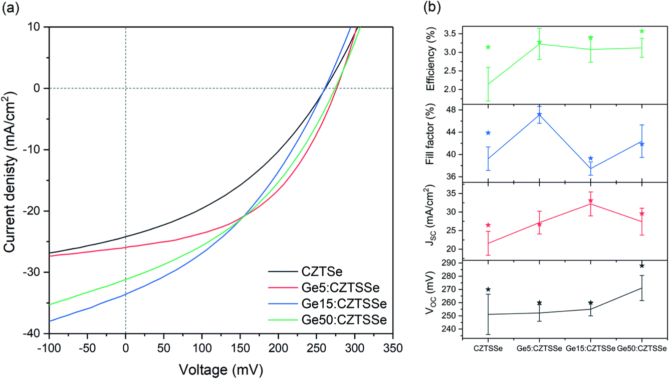 | ||
| Fig. 6 CZTSSe device performance (a). J–V characteristics under a simulated AM1.5G spectrum and (b) statistical analysis of the performance parameters: VOC, JSC, fill factor and conversion efficiency, showing the standard deviation. | ||
The spectral response analysis of the external quantum efficiency (EQE) for the devices is presented in Fig. 7. Fig. 7a, shows a similar EQE spectra for all the devices at wavelengths below the absorption edge while disregarding the inconsistencies in device fabrication due to the thickness and quality of the buffer and TCO layers produced over a disrupted period of time (400 nm < λ < 700 nm). Notable differences are apparent in the absorption edge, reflecting the changes to the CZTSSe layer due to Ge doping (1000 nm < λ < 1400 nm). The first derivative of EQE with wavelength, depicted by the vertical dotted line, highlights a dual edge behaviour (Fig. 7b). The first inflexion point occurs at a transition energy of ∼1.18 eV and remains constant across all samples, while the inflexion peak at ∼1.13 eV shows a reduction with Ge amount, thus suggesting this could be associated with a secondary phase in the CZTSSe phase which is ameliorated by Ge doping. The observed transition energy of 1.13 eV is close to the band gap of isostructural tetragonal Cu2SnS3,24 which is a possibility given the very Zn poor surface composition. With Ge doping, this inflexion reduces, which again correlates with the increase in Zn concentration at the surface; this also matches a lowering in the Urbach energy (EU) of the tail states, often associated with Cu–Zn disorder in CZTSSe devices (Fig. 7c). The consistency of the 1.18 eV inflexion peak suggests that this is due to the bandgap of the CZTSSe, which is unexpectedly high for a 96% selenised CZTSSe. Comparing with a previous measurement of the bandgap versus chalcogen ratios, with bandgaps of Cu2ZnSnSe4 and Cu2ZnSnS4 of 1 and 1.5 eV and a bowing parameter of 0.18,25 1.18 eV corresponds to 69% Se/(S + Se), which is in close agreement with the surface Se/(S + Se) ratios estimated from XPS measurements.
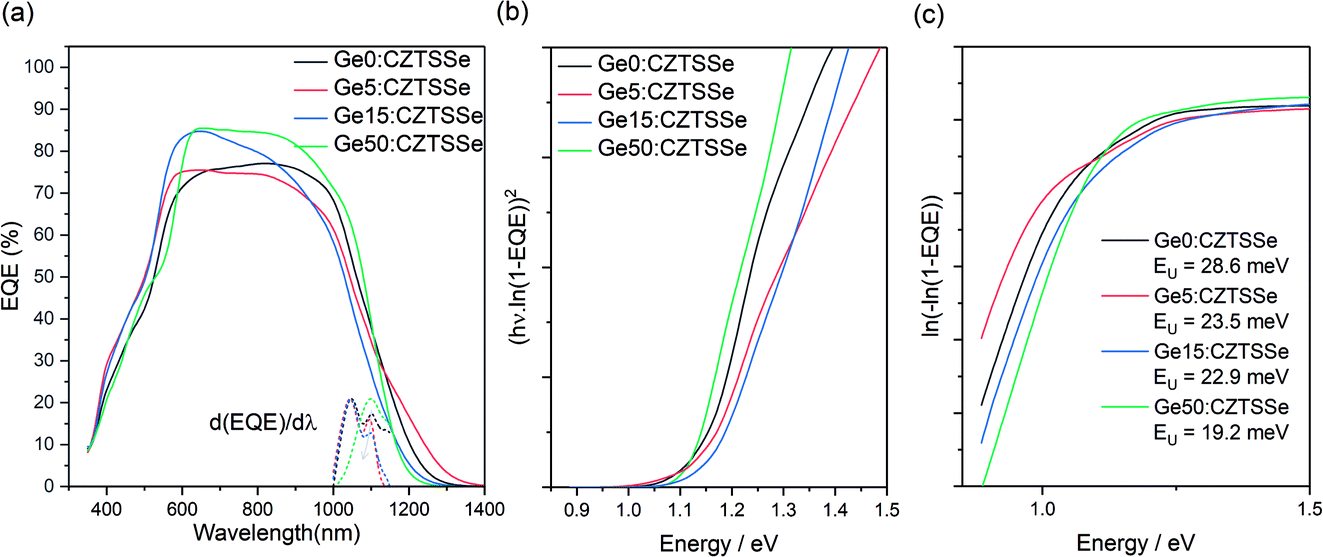 | ||
| Fig. 7 (a) EQE for CZTSSe films with and without Ge. (b) Normalised first derivative of EQE with respect to wavelength at the CZTSSe absorption edge. (c) Urbach energy determination of CZTSSe from the sub-bandgap absorption region. | ||
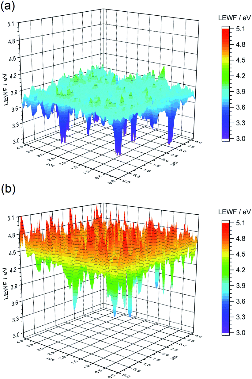
Local effective work function (LEWF) maps of CZTSSe films were constructed from the EF-PEEM spectroscopy measurements. Fig. 8 contrasts the LEWF for CZTSSe and Ge5:CZTSSe films. The LEWF map of CZTSSe without Ge displays a significant presence of low LEWF regions, as can be further visualised from the tailing of the LEWF distribution profile. The appearance of such low LEWF regions has previously been correlated with the existence of surface confined Sn(II) chalcogenide phases.26 This hypothesis further corroborates the Sn-rich composition of the CZTSSe films, as determined from XPS. The addition of Ge leads to a significant dampening of the low work function regions and a smoother surface energy landscape, as is further apparent from the absence of tailing in the LEWF distribution profile. The average LEWF of the sample without and with Ge doping, however, remains the same at around 4.54 eV. The work function of n-CdS has been reported to be between 3.8–4.0 eV from UV photoelectron spectroscopic analysis of a CZTSSe/CdS device.27 Considering the similar band-alignment, a built-in field of ∼0.65 eV is expected, which is significantly lower than the bandgap of CZTSSe films and, thus, explains the observed low VOC of the devices. We believe that this is due to the presence of Cu–Sn chalcogenide phases, as suspected from the dual-edge behaviour seen in the EQE spectra. However, Ge incorporation improves the VOC and FF of the devices, primarily by reducing the segregation of low-LEWF Sn(II) chalcogenide phases at the CZTSSe/CdS interface, thus decreasing the shunting of carriers across the interface. Furthermore, the LEWF distribution (Fig. 9c and d) shows a large broadening of the LEWF profile upon Ge incorporation (89.7 meV versus 138.2 meV without and with a 5 nm Ge underlayer, respectively). As in our previous EF-PEEM studies on CZTS and CZTSSe films derived from a molecular solution, we believe that this can be associated with an increased Cu–Zn disorder in the films.12,28 This is also in agreement with the increased asymmetry of Raman modes observed in the films.
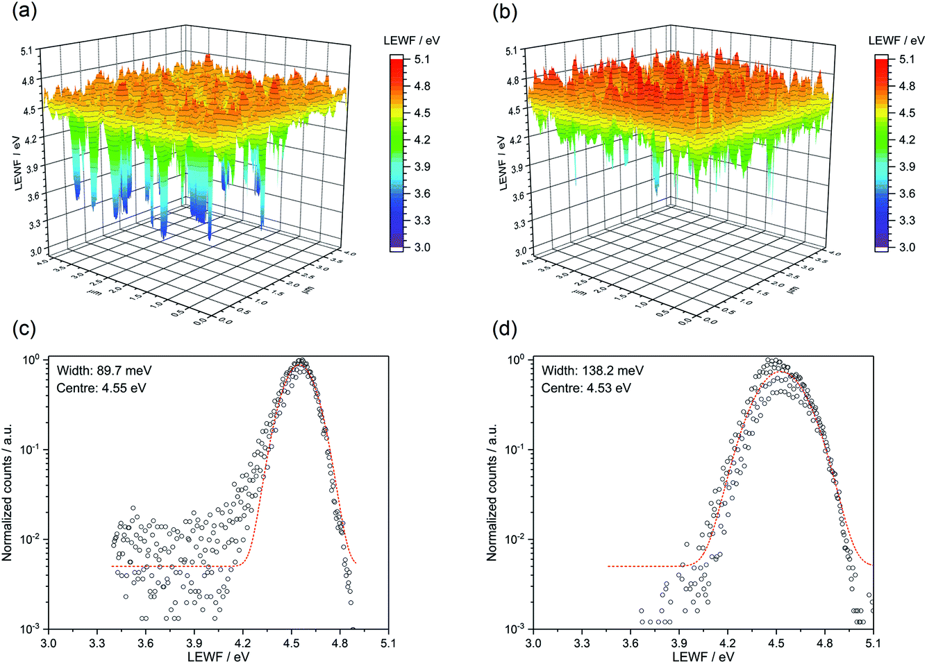 | ||
| Fig. 8 LEWF maps showing the electronic terrain for (a) CZTSSe and (b) Ge5:CZTSSe after a 500 eV Ar+ plasma etching treatment. Affiliated LEWF distribution showing the spread of points for (c) CZTSSe and (d) Ge5:CZTSSe. | ||
 | ||
| Fig. 9 LEWF maps showing the electronic terrain for the (a) CZTSSe and (b) Ge50:CZTSSe surfaces measured after heat treatment at 300 °C in UHV for 1 hour. | ||
To gain a mechanistic insight into the role of Ge doping in CZTSSe films, we deliberately induced the accelerated segregation of Sn at the surface by heating the CZTSSe films under ultra-high vacuum (UHV) conditions at 300 °C for 1 hour. From previous studies, supported by SIMS analysis, Siebentritt et al. have demonstrated the preferential migration of Sn towards front surfaces upon annealing.1,29,30Fig. 9a presents the LEWF map and distribution from CZTSSe films upon UHV heat-treatment, which clearly show a large all-around decrease in LEWF, converging to values close to those of the low-LEWF regions seen in Fig. 8a for the CZTSSe without Ge and heat treatment. This confirms extensive Sn-migration to the CZTSSe film surface. Notably, Fig. 9b shows that CZTSSe with a 50 nm Ge underlayer upon similar heat treatment greatly retains the LEWF distribution close to that of CZTSSe films not subjected to UHV heat treatment. This is a remarkable finding, indicating the strong thermodynamic stabilisation of the CZTSSe structure upon Ge doping. This increased stability is in good agreement with the work from Kim et al., who inferred a larger alloy stability for Ge-doped CZTSe through a reduced interaction parameter.10 This finding also suggests that Ge introduced through an ex situ doping route has a limited effect on somewhat crystalline phases but can, however, interact with segregated phases.
In addition to the interface, ex situ Ge-doping clearly has implications for the bulk in terms of the grain morphology, as seen in Fig. 3, a mechanism that we postulate is activated by Se vapour during selenisation. This Ge–Se interaction is reported to aid the crystallisation process through the formation of GexSey liquid phases, such as Ge3Se7, which could form a flux during selenisation.16,17 The introduction of GeSe2 has also been reported to act in a similar fashion once stabilised in a liquid GeSe2-Se system.10,19 For both analogues, and in this study, the formation of a flux means greater atomic mass transport, thus resulting in increased grain growth assisted by these growth mechanisms. Larger grains naturally lead to a reduction in grain boundaries for a film of similar thickness and are also associated with polycrystalline films of greater quality, thus reducing the number of structural defects. The effect on electronic defects cannot be quantitatively described from this study, however it is reasonable to assume that the increase in the VOC is not solely derived from the interface and that improvement in the bulk defects jointly contributes. Fig. 5 portrays a composition ratio shift in (IV)/(I + II + IV) that is compensated with respect to increased Ge doping. This Ge compensation could suppress CuSn antisite defects, which have been widely reported to cause Sn loss during selenisation;31,32 this suppression of trap states is a long-proposed mechanism in Ge doping and alloying.10,15,17 The suppression management around the Sn site may reduce the magnitude of the decomposition of CZTSSe and, by proxy, the amount of multivalency related to Sn,32 as well as the defects and related band-tailing associated with SnZn2+,7 – this is one possible narrative for the decrease in EU depicted in Fig. 7c. The retention of performance in devices with thick Ge underlayers suggests that ex situ doping has a wider operating window with respect to nanometric incorporation; this also indicates the difficulty of doping crystallised quaternary precursors efficiently. This difficulty has also been reported in preliminary work by Neuschitzer et al., in which Ge was introduced to a highly crystallised film in a so-called post deposition treatment, although this route did not yield satisfactory results and so Ge introduction to a nanocrystalline film was necessary.15 Compared to other works, we do not observe a severe deterioration in the performance metrics for devices doped with large quantities of Ge – a characteristic likely due to the nature of ex situ doping. The consistent VOC metric indicates that the level of Ge doping has not yet saturated the bulk; this saturation has been reported to cause the formation of GeCu antisite defects in Cu-poor devices and form a deep level charge carrier recombination centre.15
Conclusion
In this work, we describe an ex situ Ge doping route for CZTSSe films and solar cell devices using quaternary precursors. We describe nominal Ge incorporation through elemental depth profiling and systematic structural changes with a negligible change in the energy bandgap are measured. This set of characteristic changes evidences Ge doping as opposed to alloying. Using diffractograms and cross-sectional micrographs, we observe a substantial increase in the crystallinity and grain morphology, which is associated with a Ge–Se growth mechanism. Surface EF-PEEM measurements show an improved electronic landscape which we attribute to a reduction in the segregation of low-LEWF Sn(II) chalcogenide phases. To further improve this surface, co-doping with alkali metals, in particular Na, should be investigated to smooth the surface further. The stability of the alloy under UHV heating shows promise for the stability of the alloy; this is a key characteristic of the material within the wider photovoltaic materials subject area at present. Through the statistical analysis of J–V metrics, we report the beneficial impacts of ex situ Ge doping, including an increased VOC. We also report no large decline in the performance with higher Ge doping amounts, which suggests a limited impact that this ex situ doping route can facilitate. To further explore ex situ doping, Ge could be introduced chemically after the NC synthesis to obtain a wider distribution not reliant on high temperature annealing. Finally, we compare bulk and interface mechanisms for the VOC loss, laying the path for further surface measurements and mandating a systematic investigation of the bulk recombination mechanisms in Ge:CZTSSe thin film solar cells.Experimental methods
Sample preparation
![[thin space (1/6-em)]](https://www.rsc.org/images/entities/char_2009.gif) :Al. The N-type CdS buffer (55 nm) was deposited via a chemical bath using deionised water, cadmium sulphate, ammonium and thiourea, after which the sample was subjected to a 200 °C heat treatment in air for 20 minutes.21 The resistive i-ZnO (35 nm) layer was deposited using pulsed DC sputtering sequentially before the transparent conducting oxide ITO layer (200 nm) was deposited using RF sputtering. Front contact finger bi-layers Ni (50 nm):Al (1 μm) were evaporated sequentially via electron beam evaporation through a mask before finally, a device area of 0.16 cm2 was mechanically scribed.
:Al. The N-type CdS buffer (55 nm) was deposited via a chemical bath using deionised water, cadmium sulphate, ammonium and thiourea, after which the sample was subjected to a 200 °C heat treatment in air for 20 minutes.21 The resistive i-ZnO (35 nm) layer was deposited using pulsed DC sputtering sequentially before the transparent conducting oxide ITO layer (200 nm) was deposited using RF sputtering. Front contact finger bi-layers Ni (50 nm):Al (1 μm) were evaporated sequentially via electron beam evaporation through a mask before finally, a device area of 0.16 cm2 was mechanically scribed.
Films characterisation
Film thicknesses were measured using a stylus profilometer (DektakXT). Surface and cross-section morphologies were studied by SEM (Tescan Mira 3) at 5 kV. Elemental analysis was performed using an attached EDS detector (Oxford Instruments X-max 150) with an electron acceleration voltage of 7 kV for qualitative line scans and 20 kV for quantitative acquisitions. The crystallinity of films was studied with XRD (Rigaku SmartLab SE) using a Cu Kα radiation source (λ = 0.15406 nm) operating at 2 kW equipped with Ni CuKβ filter-sample; height alignment was performed before each acquisition. Raman spectroscopy was employed to further probe the structure using a Horiba microRaman spectrometer equipped with a 632.8 nm HeNe ion laser as the excitation source calibrated with a Si control reference. Elemental depth profiling was performed using SIMS equipped with a Hidden Analytical gas ion gun and quadrupole detector operating an Ar+ beam at 4 keV, raster area of ∼500 μm × 500 μm and a grating of 10%.Device measurements
Current–voltage measurements were performed using a source meter unit (Keithley 2400) connected to a 4-probe set-up. Solar cell devices were illuminated using a solar simulator (Abet Technologies sun 2000) at a simulated air mass (AM) 1.5 global spectrum calibrated using a c-Si reference solar cell. EQE measurements were performed using a spectral response monochromator system (Bentham Instruments M300) under illumination calibrated using a Si–InGaAs reference photodiode.X-ray photoelectron spectroscopy and energy-filtered photoemission of electron microscopy
Photoemission measurements were carried out at the Bristol NanoESCA Facility (ScientaOmicron GmbH) system. The system is made of conjoined chambers for XPS and EF-PEEM (base pressure: 2 × 10⁻¹¹ mbar). Monochromatic Al Kα (1486.7 eV) and non-monochromatic He I (21.2 eV) were used as the excitation sources for XPS and EF-PEEM, respectively. Before the EF-PEEM and XPS, the samples were treated in a preparation chamber maintained at UHV either by heating at 300 °C for 1 hour or surface cleaning with 500 eV Ar+ plasma etching for 5 min. The surface composition of the films before and after sample treatment was monitored with XPS. The EF-PEEM measurements were performed with a nominal spatial resolution of 150 nm. An energy resolution of 140 meV was calibrated from the Fermi-edge determination for a clean metallic surface when operated at room temperature with an entrance slit of 0.5 mm and a pass energy of 50 eV.Author contributions
M. C. N. and G. Z. conceptualised the project. M. C. N., D. T., D. J. F. and G. Z. established and discussed the methodology. M. C. N., B. F., X. X., M. J. and Y. Q. prepared the samples and contributed to solar cell fabrication. M. C. N., B. F., D. T., V. B., N. B., and G. Z. performed and analysed the photovoltaic measurements. M. C. N., D. T., and S. C. performed and analysed the XRD and Raman measurements. M. C. N., A. S., and P. M. performed and analysed the SEM measurements. A. S., J. L., D. T., D. J. F. and N. A. F. performed, analysed and discussed the photoelectron spectroscopy measurements. M. C. N., D. T. and G. Z. wrote the first draft of the manuscript. G. Z., D. T. and D. J. F. supervised the project. G. Z., N. S. B., V. B., D. T., D. J. F. and N. A. F. provided funding for this study. All authors have reviewed and given approval to the final version of the manuscript.Conflicts of interest
The authors declare no conflict of interest.Acknowledgements
This work was supported by the Engineering and Physical Sciences Research Council (EPSRC) via grants EP/S023836/1, EP/V008692/1, EP/V008676/1, EP/L017792/1, and EP/T005491/1. We are thankful for the EPSRC strategic equipment grants EP/K035746/1 and EP/M000605/1. The authors also appreciate the support from the North East Centre for Energy Materials (NECEM) (EP/R021503/1), the British Council Newton Fund Institutional Links Grant (CRP01286) and the Royal Society of Chemistry (E20-9404). The authors thank and acknowledge use of the University of Bristol NanoESCA II Laboratory.References
- S. Siebentritt, Thin Solid Films, 2013, 535, 1–4 CrossRef CAS.
- J. Zhou, X. Xu, B. Duan, H. Wu, J. Shi, Y. Luo, D. Li and Q. Meng, Nano Energy, 2021, 89, 106405 CrossRef CAS.
- S. Y. Chen, A. Walsh, X. G. Gong and S. H. Wei, Adv. Mater., 2013, 25, 1522–1539 CrossRef CAS PubMed.
- S. Schorr, G. Gurieva, M. Guc, M. Dimitrievska, A. Perez-Rodriguez, V. Izquierdo-Roca, C. S. Schnohr, J. Kim, W. Jo and J. M. Merino, JPhys Energy, 2020, 2, 012002 CrossRef CAS.
- S. Kim, J. S. Park and A. Walsh, ACS Energy Lett., 2018, 3, 496–500 CrossRef CAS.
- M. Kumar, A. Dubey, N. Adhikari, S. Venkatesan and Q. Qiao, Energy Environ. Sci., 2015, 8, 3134–3159 RSC.
- G. Rey, G. Larramona, S. Bourdais, C. Chone, B. Delatouche, A. Jacob, G. Dennler and S. Siebentritt, Sol. Energy Mater. Sol. Cells, 2018, 179, 142–151 CrossRef CAS.
- Y. F. Qi, Q. W. Tian, Y. N. Meng, D. X. Kou, Z. J. Zhou, W. H. Zhou and S. X. Wu, ACS Appl. Mater. Interfaces, 2017, 9, 21243–21250 CrossRef CAS PubMed.
- R. J. Sun, D. M. Zhuang, M. Zhao, Q. M. Gong, M. Scarpulla, Y. W. Wei, G. A. Ren and Y. X. Wu, Sol. Energy Mater. Sol. Cells, 2018, 174, 494–498 CrossRef CAS.
- S. Kim, K. M. Kim, H. Tampo, H. Shibata and S. Niki, Appl. Phys. Express, 2016, 9, 102301 CrossRef.
- C. J. Hages, S. Levcenco, C. K. Miskin, J. H. Alsmeier, D. Abou-Ras, R. G. Wilks, M. Bär, T. Unold and R. Agrawal, Prog. Photovoltaics, 2015, 23, 376–384 CAS.
- D. Tiwari, T. Koehler, X. Lin, R. Harniman, I. Griffiths, L. Wang, D. Cherns, R. Klenk and D. J. Fermin, Chem. Mater., 2016, 28, 4991–4997 CrossRef CAS.
- D. Tiwari, M. Cattelan, R. L. Harniman, A. Sarua, N. Fox, T. Koehler, R. Klenk and D. J. Fermin, ACS Energy Lett., 2018, 3, 2977–2982 CrossRef CAS.
- Y. E. Romanyuk, S. G. Haass, S. Giraldo, M. Placidi, D. Tiwari, D. J. Fermin, X. Hao, H. Xin, T. Schnabel and M. Kauk-Kuusik, JPhys Energy, 2019, 1, 044004 Search PubMed.
- M. Neuschitzer, J. Marquez, S. Giraldo, M. Dimitrievska, M. Placidi, I. Forbes, V. Izquierdo-Roca, A. Pérez-Rodriguez and E. Saucedo, J. Phys. Chem. C, 2016, 120, 9661–9670 CrossRef CAS.
- S. Giraldo, M. Neuschitzer, T. Thersleff, S. López-Marino, Y. Sánchez, H. Xie, M. Colina, M. Placidi, P. Pistor and V. Izquierdo-Roca, Adv. Energy Mater., 2015, 5, 1501070 CrossRef.
- S. Giraldo, E. Saucedo, M. Neuschitzer, F. Oliva, M. Placidi, X. Alcobé, V. Izquierdo-Roca, S. Kim, H. Tampo and H. Shibata, Energy Environ. Sci., 2018, 11, 582–593 RSC.
- M. Neuschitzer, M. E. Rodriguez, M. Guc, J. A. Marquez, S. Giraldo, I. Forbes, A. Perez-Rodriguez and E. Saucedo, J. Mater. Chem. A, 2018, 6, 11759–11772 RSC.
- S. Kim, K. M. Kim, H. Tampo, H. Shibata, K. Matsubara and S. Niki, Sol. Energy Mater. Sol. Cells, 2016, 144, 488–492 CrossRef CAS.
- Q. Guo, G. M. Ford, W.-C. Yang, C. J. Hages, H. W. Hillhouse and R. Agrawal, Sol. Energy Mater. Sol. Cells, 2012, 105, 132–136 CrossRef CAS.
- Y. Qu, G. Zoppi and N. S. Beattie, Progr. Photovolt.: Res. Appl., 2016, 24, 836–845 CrossRef CAS.
- S. Stølen, H. Johnsen, C. Bøe, O. Karlsen and T. Grande, J. Mater. Chem. A, 1999, 20, 17–28 Search PubMed.
- R. Sharma and Y. Chang, Bull. Alloy Phase Diagrams, 1986, 7, 68–72 CrossRef CAS.
- D. Tiwari, T. Koehler, R. Klenk and D. J. Fermin, Sustainable Energy Fuels, 2017, 1, 899–906 Search PubMed.
- X. Lin, T. Dittrich, S. Fengler, M. C. Lux-Steiner and A. Ennaoui, Appl. Phys. Lett., 2013, 102, 143903 CrossRef.
- D. Tiwari, M. Cattelan, R. L. Harniman, A. Sarua, A. Abbas, J. W. Bowers, N. A. Fox and D. J. Fermin, iScience, 2018, 9, 36–46 CrossRef CAS PubMed.
- M. Bär, T. Schnabel, J.-H. Alsmeier, S. Krause, N. Koch, R. G. Wilks and E. Ahlswede, ACS Appl. Energy Mater., 2018, 1, 475–482 CrossRef.
- D. Tiwari, M. V. Yakushev, T. Koehler, M. Cattelan, N. Fox, R. W. Martin, R. Klenk and D. J. Femin, ACS Appl. Energy Mater., 2022, 5, 3933–3940 CrossRef CAS PubMed.
- A. Redinger, K. Hönes, X. Fontané, V. Izquierdo-Roca, E. Saucedo, N. Valle, A. Pérez-Rodríguez and S. Siebentritt, Appl. Phys. Lett., 2011, 98, 101907 CrossRef.
- X. Fontané, L. Calvo-Barrio, V. Izquierdo-Roca, E. Saucedo, A. Pérez-Rodriguez, J. Morante, D. Berg, P. Dale and S. Siebentritt, Appl. Phys. Lett., 2011, 98, 181905 CrossRef.
- G. Larramona, S. Levcenko, S. Bourdais, A. Jacob, C. Choné, B. Delatouche, C. Moisan, J. Just, T. Unold and G. Dennler, Adv. Energy Mater., 2015, 5, 1501404 CrossRef.
- J. J. Scragg, T. Ericson, T. Kubart, M. Edoff and C. Platzer-Bjorkman, Chem. Mater., 2011, 23, 4625–4633 CrossRef CAS.
- Y. Qu, G. Zoppi, R. W. Miles and N. S. Beattie, Mater. Res. Express, 2014, 1, 045040 CrossRef CAS.
- Y. Qu, G. Zoppi and N. S. Beattie, Sol. Energy Mater. Sol. Cells, 2016, 158, 130–137 CrossRef CAS.
- Y. Qu, G. Zoppi, L. M. Peter, S. Jourdain and N. S. Beattie, Jpn. J. Appl. Phys., 2018, 57, 08RC01 CrossRef.
| This journal is © The Royal Society of Chemistry 2022 |